High Electron Velocity Submicrometer AlN/GaN MOS-HEMTs on ...
High Electron Velocity Submicrometer AlN/GaN MOS-HEMTs on ...
High Electron Velocity Submicrometer AlN/GaN MOS-HEMTs on ...

You also want an ePaper? Increase the reach of your titles
YUMPU automatically turns print PDFs into web optimized ePapers that Google loves.
This article has been accepted for inclusi<strong>on</strong> in a future issue of this journal. C<strong>on</strong>tent is final as presented, with the excepti<strong>on</strong> of paginati<strong>on</strong>.<br />
IEEE ELECTRON DEVICE LETTERS 1<br />
<str<strong>on</strong>g>High</str<strong>on</strong>g> <str<strong>on</strong>g>Electr<strong>on</strong></str<strong>on</strong>g> <str<strong>on</strong>g>Velocity</str<strong>on</strong>g> <str<strong>on</strong>g>Submicrometer</str<strong>on</strong>g> <str<strong>on</strong>g>AlN</str<strong>on</strong>g>/<str<strong>on</strong>g>GaN</str<strong>on</strong>g><br />
<str<strong>on</strong>g>MOS</str<strong>on</strong>g>-<str<strong>on</strong>g>HEMTs</str<strong>on</strong>g> <strong>on</strong> Freestanding <str<strong>on</strong>g>GaN</str<strong>on</strong>g> Substrates<br />
David J. Meyer, Member, IEEE, David A. Deen, Member, IEEE, David F. Storm, Mario G. Anc<strong>on</strong>a, Member, IEEE,<br />
D. Scott Katzer, Member, IEEE, Robert Bass, Jas<strong>on</strong> A. Roussos, Member, IEEE, Brian P. Downey,<br />
Steven C. Binari, Member, IEEE, Theodosia Gougousi, Tanya Paskova, Edward A. Preble, and Keith R. Evans<br />
Abstract—<str<strong>on</strong>g>AlN</str<strong>on</strong>g>/<str<strong>on</strong>g>GaN</str<strong>on</strong>g> heterostructures with 1700-cm 2 /V · s Hall<br />
mobility have been grown by molecular beam epitaxy <strong>on</strong><br />
freestanding <str<strong>on</strong>g>GaN</str<strong>on</strong>g> substrates. <str<strong>on</strong>g>Submicrometer</str<strong>on</strong>g> gate-length (L G )<br />
metal–oxide–semic<strong>on</strong>ductor (<str<strong>on</strong>g>MOS</str<strong>on</strong>g>) high-electr<strong>on</strong>-mobility transistors<br />
(<str<strong>on</strong>g>HEMTs</str<strong>on</strong>g>) fabricated from this material show excellent dc<br />
and RF performance. L G = 100 nm devices exhibited a drain<br />
current density of 1.5 A/mm, current gain cutoff frequency f T of<br />
165 GHz, a maximum frequency of oscillati<strong>on</strong> f max of 171 GHz,<br />
and intrinsic average electr<strong>on</strong> velocity v e of 1.5 × 10 7 cm/s. The<br />
40-GHz load-pull measurements of L G = 140 nm devices showed<br />
1-W/mm output power, with a 4.6-dB gain and 17% power-added<br />
efficiency. <str<strong>on</strong>g>GaN</str<strong>on</strong>g> substrates provide a way of achieving high mobility,<br />
high v e , and high RF performance in <str<strong>on</strong>g>AlN</str<strong>on</strong>g>/<str<strong>on</strong>g>GaN</str<strong>on</strong>g> transistors.<br />
Index Terms—Atomic layer depositi<strong>on</strong>, <str<strong>on</strong>g>AlN</str<strong>on</strong>g>, <str<strong>on</strong>g>GaN</str<strong>on</strong>g>, highelectr<strong>on</strong>-mobility<br />
transistors (<str<strong>on</strong>g>HEMTs</str<strong>on</strong>g>), HfO 2 , hydride vapor<br />
phase epitaxy (HVPE).<br />
I. INTRODUCTION<br />
RECENT research to increase the frequency performance<br />
of <str<strong>on</strong>g>GaN</str<strong>on</strong>g> high-electr<strong>on</strong>-mobility transistors (<str<strong>on</strong>g>HEMTs</str<strong>on</strong>g>) has<br />
focused <strong>on</strong> aggressively scaling the device geometry. As <str<strong>on</strong>g>GaN</str<strong>on</strong>g><br />
HEMT gate lengths L G are reduced below 0.25 μm, the demands<br />
of electrostatic c<strong>on</strong>trol have led to the use of novel<br />
ultrathin barriers with higher Al mole fracti<strong>on</strong>s than c<strong>on</strong>venti<strong>on</strong>al<br />
Al<str<strong>on</strong>g>GaN</str<strong>on</strong>g> alloys. For Ga-polar heterostructures, <str<strong>on</strong>g>AlN</str<strong>on</strong>g> is<br />
the thinnest pseudomorphic barrier material available that can<br />
induce (via polarizati<strong>on</strong> and c<strong>on</strong>ducti<strong>on</strong> band disc<strong>on</strong>tinuity) a<br />
2-D electr<strong>on</strong> gas (2DEG) density suitable for transistor use in<br />
<str<strong>on</strong>g>GaN</str<strong>on</strong>g> [1]. Early reports of RF devices based <strong>on</strong> the <str<strong>on</strong>g>AlN</str<strong>on</strong>g>/<str<strong>on</strong>g>GaN</str<strong>on</strong>g><br />
heterostructure showed the potential of scaling the barrier<br />
Manuscript received October 23, 2012; revised November 8, 2012; accepted<br />
November 12, 2012. This work was supported by the Office of Naval Research<br />
with funding from Dr. P. Maki. The work at the University of Maryland<br />
Baltimore County was supported in part by the Nati<strong>on</strong>al Science Foundati<strong>on</strong><br />
under Grant DMR 0846445. The review of this letter was arranged by Editor<br />
J. A. del Alamo.<br />
D. J. Meyer, D. F. Storm, M. G. Anc<strong>on</strong>a, D. S. Katzer, R. Bass, J. A. Roussos,<br />
B. P. Downey, and S. C. Binari are with the U.S. Naval Research Laboratory,<br />
Washingt<strong>on</strong>, DC 20375 USA (e-mail: david.meyer@nrl.navy.mil).<br />
D. A. Deen was with the U.S. Naval Research Laboratory, Washingt<strong>on</strong>,<br />
DC 20375 USA. He is now with the Department of Electrical and Computer<br />
Engineering, University of Minnesota, Minneapolis, MN 55455 USA (e-mail:<br />
dadeen@umn.edu).<br />
T. Gougousi is with the Department of Physics, University of Maryland-<br />
Baltimore County, Baltimore, MD 21250 USA.<br />
T. Paskova was with Kyma Technologies, Raleigh, NC 27617 USA. She is<br />
now with the Department of Material Science and Engineering, North Carolina<br />
State University, Raleigh, NC 27695 USA.<br />
E. A. Preble and K. R. Evans are with Kyma Technologies, Raleigh, NC<br />
27617 USA.<br />
Color versi<strong>on</strong>s of <strong>on</strong>e or more of the figures in this letter are available <strong>on</strong>line<br />
at http://ieeexplore.ieee.org.<br />
Digital Object Identifier 10.1109/LED.2012.2228463<br />
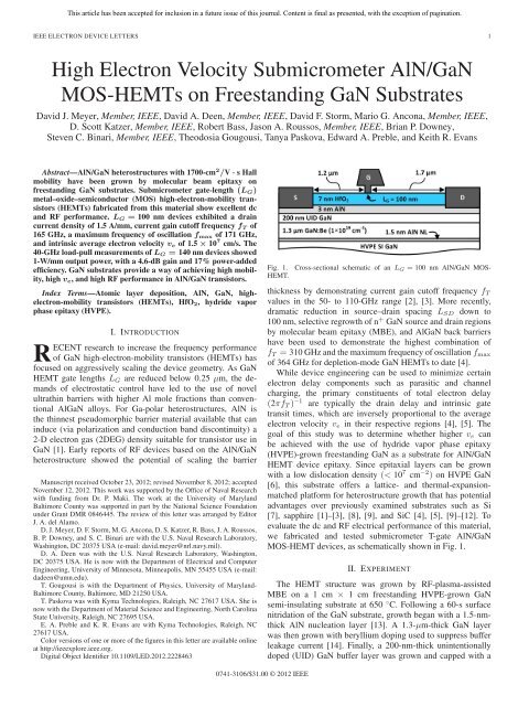
Fig. 1.<br />
HEMT.<br />
Cross-secti<strong>on</strong>al schematic of an L G = 100 nm <str<strong>on</strong>g>AlN</str<strong>on</strong>g>/<str<strong>on</strong>g>GaN</str<strong>on</strong>g> <str<strong>on</strong>g>MOS</str<strong>on</strong>g>-<br />
thickness by dem<strong>on</strong>strating current gain cutoff frequency f T<br />
values in the 50- to 110-GHz range [2], [3]. More recently,<br />
dramatic reducti<strong>on</strong> in source–drain spacing L SD down to<br />
100 nm, selective regrowth of n + <str<strong>on</strong>g>GaN</str<strong>on</strong>g> source and drain regi<strong>on</strong>s<br />
by molecular beam epitaxy (MBE), and Al<str<strong>on</strong>g>GaN</str<strong>on</strong>g> back barriers<br />
have been used to dem<strong>on</strong>strate the highest combinati<strong>on</strong> of<br />
f T = 310 GHz and the maximum frequency of oscillati<strong>on</strong> f max<br />
of 364 GHz for depleti<strong>on</strong>-mode <str<strong>on</strong>g>GaN</str<strong>on</strong>g> <str<strong>on</strong>g>HEMTs</str<strong>on</strong>g> to date [4].<br />
While device engineering can be used to minimize certain<br />
electr<strong>on</strong> delay comp<strong>on</strong>ents such as parasitic and channel<br />
charging, the primary c<strong>on</strong>stituents of total electr<strong>on</strong> delay<br />
(2πf T ) −1 are typically the drain delay and intrinsic gate<br />
transit times, which are inversely proporti<strong>on</strong>al to the average<br />
electr<strong>on</strong> velocity v e in their respective regi<strong>on</strong>s [4], [5]. The<br />
goal of this study was to determine whether higher v e can<br />
be achieved with the use of hydride vapor phase epitaxy<br />
(HVPE)-grown freestanding <str<strong>on</strong>g>GaN</str<strong>on</strong>g> as a substrate for <str<strong>on</strong>g>AlN</str<strong>on</strong>g>/<str<strong>on</strong>g>GaN</str<strong>on</strong>g><br />
HEMT device epitaxy. Since epitaxial layers can be grown<br />
with a low dislocati<strong>on</strong> density (< 10 7 cm −2 ) <strong>on</strong> HVPE <str<strong>on</strong>g>GaN</str<strong>on</strong>g><br />
[6], this substrate offers a lattice- and thermal-expansi<strong>on</strong>matched<br />
platform for heterostructure growth that has potential<br />
advantages over previously examined substrates such as Si<br />
[7], sapphire [1]–[3], [8], [9], and SiC [4], [5], [9]–[12]. To<br />
evaluate the dc and RF electrical performance of this material,<br />
we fabricated and tested submicrometer T-gate <str<strong>on</strong>g>AlN</str<strong>on</strong>g>/<str<strong>on</strong>g>GaN</str<strong>on</strong>g><br />
<str<strong>on</strong>g>MOS</str<strong>on</strong>g>-HEMT devices, as schematically shown in Fig. 1.<br />
II. EXPERIMENT<br />
The HEMT structure was grown by RF-plasma-assisted<br />
MBE <strong>on</strong> a 1 cm × 1 cm freestanding HVPE-grown <str<strong>on</strong>g>GaN</str<strong>on</strong>g><br />
semi-insulating substrate at 650 ◦ C. Following a 60-s surface<br />
nitridati<strong>on</strong> of the <str<strong>on</strong>g>GaN</str<strong>on</strong>g> substrate, growth began with a 1.5-nmthick<br />
<str<strong>on</strong>g>AlN</str<strong>on</strong>g> nucleati<strong>on</strong> layer [13]. A 1.3-μm-thick <str<strong>on</strong>g>GaN</str<strong>on</strong>g> layer<br />
was then grown with beryllium doping used to suppress buffer<br />
leakage current [14]. Finally, a 200-nm-thick unintenti<strong>on</strong>ally<br />
doped (UID) <str<strong>on</strong>g>GaN</str<strong>on</strong>g> buffer layer was grown and capped with a<br />
0741-3106/$31.00 © 2012 IEEE
This article has been accepted for inclusi<strong>on</strong> in a future issue of this journal. C<strong>on</strong>tent is final as presented, with the excepti<strong>on</strong> of paginati<strong>on</strong>.<br />
2 IEEE ELECTRON DEVICE LETTERS<br />
Fig. 2.<br />
(a) Drain and (b) transfer curves for an L G =100 nm <str<strong>on</strong>g>AlN</str<strong>on</strong>g>/<str<strong>on</strong>g>GaN</str<strong>on</strong>g> device.<br />
3-nm <str<strong>on</strong>g>AlN</str<strong>on</strong>g> barrier layer. The <str<strong>on</strong>g>GaN</str<strong>on</strong>g> layers were grown in a metalrich<br />
regime at a gallium/active nitrogen flux ratio of 1.4. The<br />
<str<strong>on</strong>g>AlN</str<strong>on</strong>g> layers were grown with an aluminum/active nitrogen flux<br />
ratio ≈1.<br />
The device fabricati<strong>on</strong> began with a Ti/Al/Ni/Au (30 nm/<br />
200 nm/40 nm/20 nm) ohmic-first process that used a premetallizati<strong>on</strong><br />
etch [15] to recess the c<strong>on</strong>tact metal prior to annealing at<br />
800 ◦ C. After annealing, the ohmic c<strong>on</strong>tact resistance was measuredtobe0.3–0.4Ω-mm<br />
using circular transfer length method<br />
patterns. Following standard Cl 2 /BCl 3 -based dry etch mesa<br />
isolati<strong>on</strong>, a 7-nm HfO 2 gate insulator was blanket deposited using<br />
tetrakis (ethylmethyl) amino hafnium (TEMAHf) and water<br />
at 250 ◦ C by atomic layer depositi<strong>on</strong>. <str<strong>on</strong>g>Submicrometer</str<strong>on</strong>g> Ni/Au<br />
(20 nm/300 nm) T-shaped gates were defined by electr<strong>on</strong>-beam<br />
lithography. The device L SD was 3 μm, gate width W G<br />
was 2 × 75 μm, and L G were 0.1, 0.14, and 2 μm. For the<br />
submicrometer T-gates, the gate head length was 0.5 μm. All<br />
dimensi<strong>on</strong>s were measured by scanning electr<strong>on</strong> microscopy.<br />
III. RESULTS AND DISCUSSION<br />
Room-temperature <strong>on</strong>-wafer Hall effect measurements were<br />
taken before and after HfO 2 depositi<strong>on</strong> to determine low-field<br />
transport properties. Prior to oxide depositi<strong>on</strong>, the average sheet<br />
resistance R sh was 194 Ω/sq with a 2DEG density of n s =<br />
1.9 × 10 13 cm −2 and mobility of 1700 cm 2 /V · s. Following<br />
oxide depositi<strong>on</strong>, R sh dropped to 164 Ω/sq with an associated<br />
increase in n s = 2.4 × 10 13 cm −2 and a slight reducti<strong>on</strong> in<br />
mobility to 1600 cm 2 /V · s. With the 2DEG n s well in excess<br />
of 10 13 cm −2 in the access regi<strong>on</strong>s, we suspect that there is<br />
sufficient Debye screening of charged dislocati<strong>on</strong>s and that the<br />
resulting mobility is therefore limited by polar optical ph<strong>on</strong><strong>on</strong><br />
scattering and interfacial roughness [1].<br />
DC electrical characteristics for an L G = 100 nm device are<br />
shown in Fig. 2. An OFF-state breakdown voltage of 35 V<br />
was measured with V GS = −7 V and 1 mA/mm of drain<br />
leakage current. Fig. 2(b) shows the transfer characteristics<br />
for the 100-nm device with a maximum current density of<br />
1.5 A/mm, a threshold voltage of approximately −6.3 V, and<br />
a subthreshold swing of 162 mV/dec (not shown). Minimal<br />
hysteresis (< 100 mV) was observed when the transfer curve<br />
was immediately swept in the reverse directi<strong>on</strong> after an initial<br />
trace. The peak transc<strong>on</strong>ductance g m,max was measured to be<br />
347 mS/mm. Intrinsic g m,max was estimated to be 419 mS/mm<br />
when the voltage drops across R s were accounted for. The<br />
sharp asymmetric shape of the transc<strong>on</strong>ductance curve is not<br />
fully understood at this time but is likely related to the dynamic<br />
Fig. 3. (a) Pad deembedded small-signal characteristics of an <str<strong>on</strong>g>AlN</str<strong>on</strong>g>/<str<strong>on</strong>g>GaN</str<strong>on</strong>g> device<br />
with L G =100 nm. (b) f T results from this study (L G =100 and 140 nm)<br />
compared with other previously reported <str<strong>on</strong>g>AlN</str<strong>on</strong>g>/<str<strong>on</strong>g>GaN</str<strong>on</strong>g> HEMT small-signal f T .<br />
Fig. 4. Equivalent circuit modeling results and extracted parameters of the<br />
L G = 100 nm <str<strong>on</strong>g>AlN</str<strong>on</strong>g>/<str<strong>on</strong>g>GaN</str<strong>on</strong>g> device in Fig. 3(a).<br />
access resistance [16] or the carrier energy clamping due to<br />
optical ph<strong>on</strong><strong>on</strong> emissi<strong>on</strong> [17].<br />
Small-signal characteristics for a <str<strong>on</strong>g>MOS</str<strong>on</strong>g>-HEMT with L G =<br />
100 nm, with pad parasitics deembedded, are shown in<br />
Fig. 3(a). f T = 165 GHz and f max = 171 GHz were determined<br />
by −20-dB/dec extrapolati<strong>on</strong> of the small-signal current<br />
gain, |h 21 |, and the maximum available gain (MAG), respectively.<br />
Prior to deembedding of probe pad parasitics (determined<br />
by cold field-effect transistor method [18]), the extrinsic<br />
f T /f max were 120 GHz/170 GHz for the L G = 100 nm device<br />
in Fig. 3(a). Pad deembedded f T /f max values of 112 GHz/<br />
134 GHz and 10 GHz/27 GHz were extracted for the 140 nm<br />
and 2-μm-L G devices, respectively. Fig. 3(b) compares the<br />
small-signal f T results from this study to literature values for<br />
<str<strong>on</strong>g>AlN</str<strong>on</strong>g>/<str<strong>on</strong>g>GaN</str<strong>on</strong>g> <str<strong>on</strong>g>HEMTs</str<strong>on</strong>g>. Despite having a relatively l<strong>on</strong>g L SD =<br />
3 μm, we observe that the f T values from the devices in this<br />
study are in line with the highest reported values at coincident<br />
L G . To investigate whether the improved small-signal performance<br />
of our devices was due to reduced parasitic effects or<br />
shorter intrinsic delay, small-signal modeling of the measured<br />
S-parameter data was c<strong>on</strong>ducted.<br />
Fig. 4 summarizes results of small-signal equivalent circuit<br />
model fitting to the measured S-parameters of the L G =<br />
100 nm <str<strong>on</strong>g>MOS</str<strong>on</strong>g>-HEMT in Fig. 3(a). [19]. Of the delays, the<br />
parasitic charging [defined as C gd · (R s + R d )] and the channel<br />
charging [calculated as (g ds /g m ) · (C gd + C gs ) · (R s + R d )]
This article has been accepted for inclusi<strong>on</strong> in a future issue of this journal. C<strong>on</strong>tent is final as presented, with the excepti<strong>on</strong> of paginati<strong>on</strong>.<br />
MEYER et al.: HIGH ELECTRON VELOCITY SUBMICROMETER <str<strong>on</strong>g>AlN</str<strong>on</strong>g>/<str<strong>on</strong>g>GaN</str<strong>on</strong>g> <str<strong>on</strong>g>MOS</str<strong>on</strong>g>-<str<strong>on</strong>g>HEMTs</str<strong>on</strong>g> 3<br />
Fig. 5.<br />
The 40-GHz power sweep of an L G = 140 nm <str<strong>on</strong>g>AlN</str<strong>on</strong>g>/<str<strong>on</strong>g>GaN</str<strong>on</strong>g> device.<br />
are relatively small percentages of the total delay (∼11%<br />
and 4%, respectively). The drain delay, i.e., C gd /g m ,ismore<br />
substantial (19%) and potentially arises from the large drain<br />
bias (8 V) causing an expansi<strong>on</strong> of the drain-side depleti<strong>on</strong><br />
regi<strong>on</strong>. The largest c<strong>on</strong>tributor to the total delay, according to<br />
our modeling, is the intrinsic gate transit time, i.e., C gs /g m .<br />
By dividing L G by the intrinsic gate transit time, intrinsic v e<br />
is calculated to be 1.53 × 10 7 cm/s for the 100-nm device. An<br />
identical analysis of a 140-nm device found the intrinsic v e to<br />
be 1.49 × 10 7 cm/s, with intrinsic gate transit and total delay<br />
times of 0.94 and 1.36 ps, respectively. These values of v e<br />
are am<strong>on</strong>g the highest reported for <str<strong>on</strong>g>AlN</str<strong>on</strong>g>/<str<strong>on</strong>g>GaN</str<strong>on</strong>g> <str<strong>on</strong>g>HEMTs</str<strong>on</strong>g>, which<br />
range from 0.8−1.5 × 10 7 cm/s [2], [4], [12]. In the case of<br />
the highest reported v e [4], velocity enhancement was achieved<br />
by laterally scaling the device to increase the lateral electric<br />
field across the intrinsic device. We speculate that the elevated<br />
velocity in this study is not due to velocity enhancement but,<br />
instead, is a result of using epitaxial material grown <strong>on</strong> HVPE<br />
<str<strong>on</strong>g>GaN</str<strong>on</strong>g>, where low dislocati<strong>on</strong> densities in the low-field porti<strong>on</strong><br />
of the intrinsic device result in minimal mobility degradati<strong>on</strong><br />
when the gate is biased for peak f T (and n sh is reduced <<br />
1 × 10 13 cm −2 ) [20]. In higher dislocati<strong>on</strong> density material, the<br />
depleti<strong>on</strong> of the 2DEG underneath the gate metal, when biased<br />
for peak f T , could significantly reduce the Debye screening of<br />
charged dislocati<strong>on</strong>s and render electr<strong>on</strong> transport susceptible<br />
to Coulombic scattering and, c<strong>on</strong>sequently, lower intrinsic v e .<br />
To evaluate the large-signal potential of these devices, 500-ns<br />
pulsed gate lag measurements were performed at quiescent<br />
biases of V DS = 10 V and V GS = −7 V and showed gate<br />
lag ratios (pulsed I DSS /dc I DSS ) of 0.8–1.0 for all devices in<br />
this study. Subsequent <strong>on</strong>-wafer 40-GHz load-pull measurements<br />
taken <strong>on</strong> a 140-nm device biased in class AB (V DS =<br />
10 V, and V GS = −4.5 V) gave the results shown in Fig. 5.<br />
At the peak power-added efficiency (PAE) of 17%, the gain<br />
was 4.6 dB, and the output power density was 1 W/mm. This<br />
result shows the potential for <str<strong>on</strong>g>AlN</str<strong>on</strong>g>/<str<strong>on</strong>g>GaN</str<strong>on</strong>g> <str<strong>on</strong>g>HEMTs</str<strong>on</strong>g> to produce<br />
millimeter-wavelength power.<br />
IV. CONCLUSION<br />
To the best of our knowledge, this is the first dem<strong>on</strong>strati<strong>on</strong><br />
of an <str<strong>on</strong>g>AlN</str<strong>on</strong>g>/<str<strong>on</strong>g>GaN</str<strong>on</strong>g> <str<strong>on</strong>g>MOS</str<strong>on</strong>g>-HEMT <strong>on</strong> freestanding <str<strong>on</strong>g>GaN</str<strong>on</strong>g>. Epitaxial<br />
growth <strong>on</strong> HVPE <str<strong>on</strong>g>GaN</str<strong>on</strong>g> has been shown to yield submicrometer<br />
devices with excellent dc and RF performance. Reflective of<br />
the material quality, a high value of intrinsic average electr<strong>on</strong><br />
velocity (v e = 1.5 × 10 7 cm/s) was extracted for these devices.<br />
REFERENCES<br />
[1] Y. Cao and D. Jena, “<str<strong>on</strong>g>High</str<strong>on</strong>g>-mobility window for two-dimensi<strong>on</strong>al electr<strong>on</strong><br />
gases at ultrathin <str<strong>on</strong>g>AlN</str<strong>on</strong>g>/<str<strong>on</strong>g>GaN</str<strong>on</strong>g> heterojuncti<strong>on</strong>s,” Appl. Phys. Lett., vol. 90,<br />
no. 18, p. 182 112-3, Apr. 2007.<br />
[2] M. Higashiwaki, T. Mimura, and T. Matsui, “<str<strong>on</strong>g>AlN</str<strong>on</strong>g>/<str<strong>on</strong>g>GaN</str<strong>on</strong>g> insulated-gate<br />
HFETs using Cat-CVD SiN,” IEEE <str<strong>on</strong>g>Electr<strong>on</strong></str<strong>on</strong>g> Device Lett., vol. 27, no. 9,<br />
pp. 719–721, Sep. 2006.<br />
[3] T.Zimmermann,D.Deen,Y.Cao,J.Sim<strong>on</strong>,P.Fay,D.Jena,andH.G.<br />
Xing, “<str<strong>on</strong>g>AlN</str<strong>on</strong>g>/<str<strong>on</strong>g>GaN</str<strong>on</strong>g> insulated-gate <str<strong>on</strong>g>HEMTs</str<strong>on</strong>g> with 2.3 A/mm output current<br />
and 480 mS/mm transc<strong>on</strong>ductance,” IEEE <str<strong>on</strong>g>Electr<strong>on</strong></str<strong>on</strong>g> Device Lett., vol. 29,<br />
no. 7, pp. 661–664, Jul. 2008.<br />
[4] K. Shinohara, D. Regan, A. Corri<strong>on</strong>, D. Brown, S. Burnham, P. J.<br />
Willadsen, I. Alvarado-Rodriguez, M. Cunningham, C. Butler, A. Schmitz,<br />
S. Kim, B. Holden, D. Chang, V. Lee, A. Ohoka, P. M. Asbeck, and<br />
M. Micovic, “Deeply-scaled self-aligned-gate <str<strong>on</strong>g>GaN</str<strong>on</strong>g> DH-<str<strong>on</strong>g>HEMTs</str<strong>on</strong>g> with ultrahigh<br />
cutoff frequency,” in IEDM Tech. Dig., 2011, pp. 453–456.<br />
[5] K. Shinohara, D. Regan, I. Milosavljevic, A. L. Corri<strong>on</strong>, D. F. Brown, P. J.<br />
Willadsen, C. Butler, A. Schmitz, S. Kim, V. Lee, A. Ohoka, P. M. Asbeck,<br />
and M. Micovic, “<str<strong>on</strong>g>Electr<strong>on</strong></str<strong>on</strong>g> velocity enhancement in laterally scaled <str<strong>on</strong>g>GaN</str<strong>on</strong>g><br />
DH-<str<strong>on</strong>g>HEMTs</str<strong>on</strong>g> with f T of 260 GHz,” IEEE <str<strong>on</strong>g>Electr<strong>on</strong></str<strong>on</strong>g> Device Lett., vol. 32,<br />
no. 8, pp. 1074–1076, Aug. 2011.<br />
[6] D. F. Storm, D. S. Katzer, J. A. Roussos, J. A. Mittereder, R. Bass,<br />
S. C. Binari, L. Zhou, D. J. Smith, D. Hanser, E. A. Preble, and K. R.<br />
Evans, “Microwave performance and structural characterizati<strong>on</strong> of MBEgrown<br />
Al<str<strong>on</strong>g>GaN</str<strong>on</strong>g>/<str<strong>on</strong>g>GaN</str<strong>on</strong>g> <str<strong>on</strong>g>HEMTs</str<strong>on</strong>g> <strong>on</strong> low dislocati<strong>on</strong> density <str<strong>on</strong>g>GaN</str<strong>on</strong>g> substrates,”<br />
J. Cryst. Growth, vol. 305, no. 2, pp. 340–345, Jul. 2007.<br />
[7] F. Medjdoub, M. Zegaoui, N. Waldhoff, B. Grimbert, N. Rolland, and<br />
P.-A. Rolland, “Above 600 mS/mm transc<strong>on</strong>ductance with 2.3 A/mm<br />
drain current density <str<strong>on</strong>g>AlN</str<strong>on</strong>g>/<str<strong>on</strong>g>GaN</str<strong>on</strong>g> high-electr<strong>on</strong>-mobility transistors grown<br />
<strong>on</strong> silic<strong>on</strong>,” Appl. Phys. Exp., vol. 4, p. 064106, Jun. 2011.<br />
[8] K. D. Chabak, D. E. Walker, M. R. Johns<strong>on</strong>, A. Crespo, A. M. Dabiran,<br />
D. J. Smith, A. M. Wowchak, S. K. Tetlak, M. Kossler, J. K. Gillespie,<br />
R. C. Fitch, and M. Trejo, “<str<strong>on</strong>g>High</str<strong>on</strong>g>-performance <str<strong>on</strong>g>AlN</str<strong>on</strong>g>/<str<strong>on</strong>g>GaN</str<strong>on</strong>g> <str<strong>on</strong>g>HEMTs</str<strong>on</strong>g> <strong>on</strong><br />
sapphire substrate with an oxidized gate insulator,” IEEE <str<strong>on</strong>g>Electr<strong>on</strong></str<strong>on</strong>g> Device<br />
Lett., vol. 32, no. 12, pp. 1677–1679, Dec. 2011.<br />
[9] A. M. Dabiran, A. M. Wowchak, A. Osinsky, J. Xie, B. Hertog, B. Cui,<br />
D. C. Look, and P. P. Chow, “Very high channel c<strong>on</strong>ductivity in low-defect<br />
<str<strong>on</strong>g>AlN</str<strong>on</strong>g>/<str<strong>on</strong>g>GaN</str<strong>on</strong>g> high electr<strong>on</strong> mobility transistor structures,” Appl. Phys. Lett.,<br />
vol. 93, no. 8, p. 082 111-3, Aug. 2008.<br />
[10] D. A. Deen, S. C. Binari, D. F. Storm, D. S. Katzer, J. A. Roussos, J. C.<br />
Hackley, and T. Gougousi, “AIN/<str<strong>on</strong>g>GaN</str<strong>on</strong>g> insulated gate <str<strong>on</strong>g>HEMTs</str<strong>on</strong>g> with HfO 2<br />
gate dielectric,” <str<strong>on</strong>g>Electr<strong>on</strong></str<strong>on</strong>g>. Lett., vol. 45, no. 8, pp. 423–424, Apr. 2009.<br />
[11] D. A. Deen, D. F. Storm, R. Bass, D. J. Meyer, D. S. Katzer, S. C. Binari,<br />
J. W. Lacis, and T. Gougousi, “Atomic layer deposited Ta 2 O 5 gate insulati<strong>on</strong><br />
for enhancing breakdown voltage of <str<strong>on</strong>g>AlN</str<strong>on</strong>g>/<str<strong>on</strong>g>GaN</str<strong>on</strong>g> high electr<strong>on</strong> mobility<br />
transistors,” Appl. Phys. Lett., vol. 98, no. 2, p. 023506-3, Jan. 2011.<br />
[12] K. Shinohara, A. Corri<strong>on</strong>, D. Regan, I. Milosavljevic, D. Brown, S. Burnham,<br />
P. J. Willadsen, C. Butler, A. Schmitz, D. Wheeler, A. Fung, and M. Micovic,<br />
“220 GHz f T and 400 GHz f max in 40-nm <str<strong>on</strong>g>GaN</str<strong>on</strong>g> DH-<str<strong>on</strong>g>HEMTs</str<strong>on</strong>g> with regrown<br />
ohmic,” in Proc. IEDM Tech. Dig., 2010, pp. 672–675.<br />
[13] Y. Cao, T. Zimmermann, H. Xing, and D. Jena, “Polarizati<strong>on</strong>-engineered<br />
removal of buffer leakage for <str<strong>on</strong>g>GaN</str<strong>on</strong>g> transistors,” Appl. Phys. Lett., vol. 96,<br />
no. 4, p. 042102-3, Jan. 2010.<br />
[14] D. F. Storm, D. S. Katzer, D. A. Deen, R. Bass, D. J. Meyer, J. A. Roussos,<br />
S. C. Binari, T. Paskova, E. A. Preble, and K. R. Evans, “Proximity<br />
effects of beryllium-doped <str<strong>on</strong>g>GaN</str<strong>on</strong>g> buffer layers <strong>on</strong> the electr<strong>on</strong>ic properties<br />
of epitaxial Al<str<strong>on</strong>g>GaN</str<strong>on</strong>g>/<str<strong>on</strong>g>GaN</str<strong>on</strong>g> heterostructures,” Solid State <str<strong>on</strong>g>Electr<strong>on</strong></str<strong>on</strong>g>., vol. 54,<br />
no. 11, pp. 1470–1473, Nov. 2010.<br />
[15] D. A. Deen, D. F. Storm, D. S. Katzer, D. J. Meyer, and S. C. Binari, “Dependence<br />
of ohmic c<strong>on</strong>tact resistance <strong>on</strong> barrier thickness of <str<strong>on</strong>g>AlN</str<strong>on</strong>g>/<str<strong>on</strong>g>GaN</str<strong>on</strong>g><br />
HEMT structures,” Solid State <str<strong>on</strong>g>Electr<strong>on</strong></str<strong>on</strong>g>., vol. 54, no. 6, pp. 613–615,<br />
Jun. 2010.<br />
[16] T. Palacios, S. Rajan, A. Chakraborty, S. Heikman, S. Keller, S. P.<br />
DenBaars, and U. K. Mishra, “Influence of the dynamic access resistance<br />
in the g m and f T linearity of Al<str<strong>on</strong>g>GaN</str<strong>on</strong>g>/<str<strong>on</strong>g>GaN</str<strong>on</strong>g> <str<strong>on</strong>g>HEMTs</str<strong>on</strong>g>,” IEEE Trans.<br />
<str<strong>on</strong>g>Electr<strong>on</strong></str<strong>on</strong>g> Devices, vol. 52, no. 10, pp. 2117–2123, Oct. 2005.<br />
[17] T. Fang, R. Wang, H. Xing, S. Rajan, and D. Jena, “Effect of optical<br />
ph<strong>on</strong><strong>on</strong> scattering <strong>on</strong> the performance of <str<strong>on</strong>g>GaN</str<strong>on</strong>g> transistors,” IEEE <str<strong>on</strong>g>Electr<strong>on</strong></str<strong>on</strong>g><br />
Device Lett., vol. 33, no. 5, pp. 709–711, May 2012.<br />
[18] G. Dambrine, A. Cappy, F. Heliodore, and E. Playez, “A new method<br />
for determining the FET small-signal equivalent circuit,” IEEE Trans.<br />
Microw. Theory Tech., vol. 36, no. 7, pp. 1151–1159, Jul. 1988.<br />
[19] P. J. Tasker and B. Hughes, “Importance of source and drain resistance to<br />
the maximum f T of millimeter-wave MODFETs,” IEEE <str<strong>on</strong>g>Electr<strong>on</strong></str<strong>on</strong>g> Device<br />
Lett., vol. 10, no. 7, pp. 291–293, Jul. 1989.<br />
[20] D. Jena, A. C. Gossard, and U. K. Mishra, “Dislocati<strong>on</strong> scattering in<br />
a two-dimensi<strong>on</strong>al electr<strong>on</strong> gas,” Appl. Phys. Lett., vol. 76, no. 13,<br />
pp. 1707–1709, Mar. 2000.