I C Precision Altimeter - Farnell
I C Precision Altimeter - Farnell
I C Precision Altimeter - Farnell

You also want an ePaper? Increase the reach of your titles
YUMPU automatically turns print PDFs into web optimized ePapers that Google loves.
Freescale Semiconductor<br />
Document Number: MPL3115A2<br />
Data Sheet: Advance Information Rev 2, 04/2012<br />
An Energy Efficient Solution by Freescale<br />
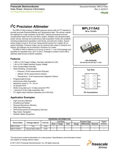
I 2 C <strong>Precision</strong> <strong>Altimeter</strong><br />
The MPL3115A2 employs a MEMS pressure sensor with an I 2 C interface to<br />
provide accurate Pressure/Altitude and Temperature data. The sensor outputs<br />
are digitized by a high resolution 24-bit ADC. Internal processing removes<br />
compensation tasks from the host MCU system. Multiple user-programmable,<br />
power saving, interrupt and autonomous data acquisition modes are available,<br />
including programmed acquisition cycle timing, and poll-only modes. Typical<br />
active supply current is 40 μA per measurement-second for a stable 30 cm<br />
output resolution. Pressure output can be resolved with output in fractions of a<br />
Pascal, and Altitude can be resolved in fractions of a meter.<br />
The MPL3115A2 is offered in a 5 mm by 3 mm by 1.1 mm LGA package and<br />
specified for operation from -40°C to 85°C. Package is surface mount with a<br />
stainless steel lid and is RoHS compliant.<br />
Features<br />
• 1.95V to 3.6V Supply Voltage, internally regulated by LDO<br />
• 1.6V to 3.6V Digital Interface Supply Voltage<br />
• Fully Compensated internally<br />
• Direct Reading, Compensated<br />
– Pressure: 20-bit measurement (Pascals)<br />
– Altitude: 20-bit measurement (meters)<br />
– Temperature: 12-bit measurement (degrees Celsius)<br />
• Programmable Events<br />
• Autonomous Data Acquisition<br />
• Resolution down to 1 ft. / 30 cm<br />
• 32 Sample FIFO<br />
• Ability to log data up to 12 days using the FIFO<br />
• 1 second to 9 hour data acquisition rate<br />
• I 2 C digital output interface (operates up to 400 kHz)<br />
MPL3115A2<br />
50 to 110 kPa<br />
LGA PACKAGE<br />
5.0 mm by 3.0 mm by 1.1 mm<br />
V DD<br />
CAP<br />
GND<br />
V DDIO<br />
Top View<br />
1<br />
2<br />
3<br />
4<br />
Pin Connections<br />
8<br />
7<br />
6<br />
5<br />
SCL<br />
SDA<br />
INT1<br />
INT2<br />
Application Examples<br />
• High Accuracy Altimetry<br />
• Smartphones/Tablets<br />
• Personal Electronics Altimetry<br />
• GPS Dead Reckoning<br />
• GPS Enhancement for Emergency Services<br />
• Map Assist, Navigation<br />
• Weather Station Equipment<br />
ORDERING INFORMATION<br />
Device Name Package Options Case No.<br />
# of Ports Pressure Type Digital<br />
None Single Dual Gauge Differential Absolute Interface<br />
MPL3115A2 Tray 2153 • • •<br />
MPL3115A2T1 Tape & Reel (1000) 2153 • • •<br />
This document contains information on a new product. Specifications and information herein<br />
are subject to change without notice.<br />
© 2011-2012 Freescale Semiconductor, Inc. All rights reserved.
Contents<br />
1 Block Diagram and Pin Descriptions . . . . . . . . . . . . . . . . . . . . . . . . . . . . . . . . . . . . . . . . . . . . . . . . . . . . . . . . . . . . . . . . 3<br />
2 Mechanical and Electrical Specifications . . . . . . . . . . . . . . . . . . . . . . . . . . . . . . . . . . . . . . . . . . . . . . . . . . . . . . . . . . . . 5<br />
2.1 Mechanical Characteristics . . . . . . . . . . . . . . . . . . . . . . . . . . . . . . . . . . . . . . . . . . . . . . . . . . . . . . . . . . . . . . . . . . . . . 5<br />
3 Electrical Characteristics . . . . . . . . . . . . . . . . . . . . . . . . . . . . . . . . . . . . . . . . . . . . . . . . . . . . . . . . . . . . . . . . . . . . . . . . . 6<br />
3.1 I 2 C Interface Characteristics. . . . . . . . . . . . . . . . . . . . . . . . . . . . . . . . . . . . . . . . . . . . . . . . . . . . . . . . . . . . . . . . . . . . 7<br />
3.2 Absolute Maximum Ratings . . . . . . . . . . . . . . . . . . . . . . . . . . . . . . . . . . . . . . . . . . . . . . . . . . . . . . . . . . . . . . . . . . . . 9<br />
4 Quick Start Quick Setup Guide . . . . . . . . . . . . . . . . . . . . . . . . . . . . . . . . . . . . . . . . . . . . . . . . . . . . . . . . . . . . . . . . . . . . 10<br />
5 Terminology . . . . . . . . . . . . . . . . . . . . . . . . . . . . . . . . . . . . . . . . . . . . . . . . . . . . . . . . . . . . . . . . . . . . . . . . . . . . . . . . . . . 14<br />
5.1 Resolution. . . . . . . . . . . . . . . . . . . . . . . . . . . . . . . . . . . . . . . . . . . . . . . . . . . . . . . . . . . . . . . . . . . . . . . . . . . . . . . . . 14<br />
5.2 Accuracy . . . . . . . . . . . . . . . . . . . . . . . . . . . . . . . . . . . . . . . . . . . . . . . . . . . . . . . . . . . . . . . . . . . . . . . . . . . . . . . . . . 14<br />
5.3 Pressure/Altitude. . . . . . . . . . . . . . . . . . . . . . . . . . . . . . . . . . . . . . . . . . . . . . . . . . . . . . . . . . . . . . . . . . . . . . . . . . . . 14<br />
5.4 Power Modes of Operation . . . . . . . . . . . . . . . . . . . . . . . . . . . . . . . . . . . . . . . . . . . . . . . . . . . . . . . . . . . . . . . . . . . . 15<br />
6 Functionality . . . . . . . . . . . . . . . . . . . . . . . . . . . . . . . . . . . . . . . . . . . . . . . . . . . . . . . . . . . . . . . . . . . . . . . . . . . . . . . . . . . 15<br />
6.1 Factory Calibration. . . . . . . . . . . . . . . . . . . . . . . . . . . . . . . . . . . . . . . . . . . . . . . . . . . . . . . . . . . . . . . . . . . . . . . . . . 16<br />
6.2 Barometer/<strong>Altimeter</strong> Function . . . . . . . . . . . . . . . . . . . . . . . . . . . . . . . . . . . . . . . . . . . . . . . . . . . . . . . . . . . . . . . . . . 16<br />
6.3 Temperature Function. . . . . . . . . . . . . . . . . . . . . . . . . . . . . . . . . . . . . . . . . . . . . . . . . . . . . . . . . . . . . . . . . . . . . . . . 16<br />
6.4 Autonomous Data Acquisition. . . . . . . . . . . . . . . . . . . . . . . . . . . . . . . . . . . . . . . . . . . . . . . . . . . . . . . . . . . . . . . . . . 16<br />
6.5 FIFO . . . . . . . . . . . . . . . . . . . . . . . . . . . . . . . . . . . . . . . . . . . . . . . . . . . . . . . . . . . . . . . . . . . . . . . . . . . . . . . . . . . . 16<br />
6.6 External Interrupts. . . . . . . . . . . . . . . . . . . . . . . . . . . . . . . . . . . . . . . . . . . . . . . . . . . . . . . . . . . . . . . . . . . . . . . . . . . 16<br />
6.7 Pressure/Altitude and Temperature Delta. . . . . . . . . . . . . . . . . . . . . . . . . . . . . . . . . . . . . . . . . . . . . . . . . . . . . . . . . 17<br />
6.8 Min/Max Data Value Storage . . . . . . . . . . . . . . . . . . . . . . . . . . . . . . . . . . . . . . . . . . . . . . . . . . . . . . . . . . . . . . . . . . 17<br />
6.9 Digital Interface . . . . . . . . . . . . . . . . . . . . . . . . . . . . . . . . . . . . . . . . . . . . . . . . . . . . . . . . . . . . . . . . . . . . . . . . . . . . 17<br />
7 Register Descriptions. . . . . . . . . . . . . . . . . . . . . . . . . . . . . . . . . . . . . . . . . . . . . . . . . . . . . . . . . . . . . . . . . . . . . . . . . . . . 19<br />
7.1 Sensor Status . . . . . . . . . . . . . . . . . . . . . . . . . . . . . . . . . . . . . . . . . . . . . . . . . . . . . . . . . . . . . . . . . . . . . . . . . . . . . . 21<br />
7.2 Device ID . . . . . . . . . . . . . . . . . . . . . . . . . . . . . . . . . . . . . . . . . . . . . . . . . . . . . . . . . . . . . . . . . . . . . . . . . . . . . . . . . 25<br />
7.3 FIFO Setup . . . . . . . . . . . . . . . . . . . . . . . . . . . . . . . . . . . . . . . . . . . . . . . . . . . . . . . . . . . . . . . . . . . . . . . . . . . . . . . . 25<br />
7.4 Time Delay Register . . . . . . . . . . . . . . . . . . . . . . . . . . . . . . . . . . . . . . . . . . . . . . . . . . . . . . . . . . . . . . . . . . . . . . . . 27<br />
7.5 System Mode Register . . . . . . . . . . . . . . . . . . . . . . . . . . . . . . . . . . . . . . . . . . . . . . . . . . . . . . . . . . . . . . . . . . . . . . . 27<br />
7.6 System Interrupt Status . . . . . . . . . . . . . . . . . . . . . . . . . . . . . . . . . . . . . . . . . . . . . . . . . . . . . . . . . . . . . . . . . . . . . . 27<br />
7.7 Sensor Data . . . . . . . . . . . . . . . . . . . . . . . . . . . . . . . . . . . . . . . . . . . . . . . . . . . . . . . . . . . . . . . . . . . . . . . . . . . . . . . 28<br />
7.8 Barometric Pressure Input . . . . . . . . . . . . . . . . . . . . . . . . . . . . . . . . . . . . . . . . . . . . . . . . . . . . . . . . . . . . . . . . . . . . 29<br />
7.9 Pressure/Altitude Target . . . . . . . . . . . . . . . . . . . . . . . . . . . . . . . . . . . . . . . . . . . . . . . . . . . . . . . . . . . . . . . . . . . . . . 29<br />
7.10 Temperature Target . . . . . . . . . . . . . . . . . . . . . . . . . . . . . . . . . . . . . . . . . . . . . . . . . . . . . . . . . . . . . . . . . . . . . . . . . 29<br />
7.11 Pressure/Altitude Window. . . . . . . . . . . . . . . . . . . . . . . . . . . . . . . . . . . . . . . . . . . . . . . . . . . . . . . . . . . . . . . . . . . . . 30<br />
7.12 Temperature Window . . . . . . . . . . . . . . . . . . . . . . . . . . . . . . . . . . . . . . . . . . . . . . . . . . . . . . . . . . . . . . . . . . . . . . . . 30<br />
7.13 Minimum Pressure . . . . . . . . . . . . . . . . . . . . . . . . . . . . . . . . . . . . . . . . . . . . . . . . . . . . . . . . . . . . . . . . . . . . . . . . . . 30<br />
7.14 Maximum Pressure. . . . . . . . . . . . . . . . . . . . . . . . . . . . . . . . . . . . . . . . . . . . . . . . . . . . . . . . . . . . . . . . . . . . . . . . . . 31<br />
7.15 Minimum Temperature . . . . . . . . . . . . . . . . . . . . . . . . . . . . . . . . . . . . . . . . . . . . . . . . . . . . . . . . . . . . . . . . . . . . . . . 31<br />
7.16 Maximum Temperature. . . . . . . . . . . . . . . . . . . . . . . . . . . . . . . . . . . . . . . . . . . . . . . . . . . . . . . . . . . . . . . . . . . . . . . 32<br />
7.17 Control Registers . . . . . . . . . . . . . . . . . . . . . . . . . . . . . . . . . . . . . . . . . . . . . . . . . . . . . . . . . . . . . . . . . . . . . . . . . . . 32<br />
7.18 Offset Correction. . . . . . . . . . . . . . . . . . . . . . . . . . . . . . . . . . . . . . . . . . . . . . . . . . . . . . . . . . . . . . . . . . . . . . . . . . . . 37<br />
8 Soldering/Landing Pad Information . . . . . . . . . . . . . . . . . . . . . . . . . . . . . . . . . . . . . . . . . . . . . . . . . . . . . . . . . . . . . . . . 39<br />
9 Tape and Reel Specifications . . . . . . . . . . . . . . . . . . . . . . . . . . . . . . . . . . . . . . . . . . . . . . . . . . . . . . . . . . . . . . . . . . . . . 42<br />
Related Documentation<br />
The MPL3115A2 device features and operations are described in a variety of reference manuals, user guides, and application<br />
notes. To find the most-current versions of these documents:<br />
1. Go to the Freescale homepage at:<br />
MPL3115A2<br />
http://www.freescale.com/<br />
2. In the Keyword search box at the top of the page, enter the device number MPL3115A2.<br />
3. In the Refine Your Result pane on the left, click on the Documentation link.<br />
Sensors<br />
2 Freescale Semiconductor, Inc.
1 Block Diagram and Pin Descriptions<br />
Reference<br />
Reference<br />
+<br />
Regulator<br />
Regulator<br />
VVdd<br />
DD<br />
VddIO<br />
V DDIO<br />
CAP<br />
SDA<br />
Pressure<br />
Sensor<br />
Sense<br />
Amp<br />
Temp<br />
MUX<br />
ADC<br />
Digital Signal<br />
Processing and<br />
Control<br />
SCL<br />
INT1<br />
INT2<br />
Clock oscillator<br />
Clock Oscillator<br />
Trim Logic<br />
Trim Logic<br />
Figure 1. Block Diagram<br />
Table 1. Pin Descriptions<br />
Pin Name Function<br />
1 V DD V DD Power Supply Connection (1.95-3.6V)<br />
2 CAP External Capacitor<br />
3 GND Ground<br />
4 V DDIO Digital Interface Power Supply (1.62-3.6V)<br />
5 INT2 Pressure Interrupt 2<br />
6 INT1 Pressure Interrupt 1<br />
7 SDA I 2 C Serial Data<br />
8 SCL I 2 C Serial Clock<br />
MPL3115A2<br />
Sensors<br />
Freescale Semiconductor, Inc. 3
Vdd<br />
V DD<br />
2<br />
100nF<br />
10μF<br />
1 8<br />
SCL<br />
7<br />
SDA<br />
100nF<br />
3<br />
6<br />
INT1<br />
V<br />
VddIO DDIO<br />
4 5<br />
INT2<br />
Figure 2. Pin Connections<br />
The device power is supplied through the V DD line. Power supply decoupling capacitors (100 nF ceramic plus 10 μF bulk or<br />
10 μF ceramic) should be placed as near as possible to pin 1 of the device. A second 100 nF capacitor is used to bypass the<br />
internal regulator. The functions, threshold and the timing of the interrupt pins (INT1 and INT2) are user programmable through<br />
the I 2 C interface.<br />
MPL3115A2<br />
Sensors<br />
4 Freescale Semiconductor, Inc.
2 Mechanical and Electrical Specifications<br />
2.1 Mechanical Characteristics<br />
Table 2. Mechanical Characteristics @ V DD = 2.5V, T = 25°C unless otherwise noted (1)<br />
Ref Symbol Parameter Test Conditions Min Typ Max Unit<br />
Pressure Sensor<br />
1 P FS Measurement Range<br />
2 Pressure Reading Noise<br />
Calibrated Range 50 110 kPa<br />
Operational Range 20 110 kPa<br />
1x Oversample (2)<br />
19 Pa RMS<br />
128x Oversample (2) 1.5 Pa RMS<br />
3 Pressure Absolute Accuracy<br />
50 to 110 kPa<br />
over 0°C to 50°C<br />
50 to 110 kPa<br />
over -10°C to 70°C<br />
-0.4 0.4<br />
±0.4<br />
kPa<br />
4 Pressure Relative Accuracy<br />
Relative accuracy during<br />
pressure change between<br />
70 to 110 kPa at any constant<br />
temperature between<br />
-10°C to 50°C<br />
Relative accuracy during<br />
changing temperature between<br />
-10°C to 50°C at any constant<br />
pressure between 50 kPa to 110<br />
kPa<br />
±0.05<br />
±0.1<br />
kPa<br />
5 Pressure/Altitude Resolution (3)(4)(5)<br />
6 Output Data Rate<br />
Barometer Mode 0.25 1.5 Pa<br />
<strong>Altimeter</strong> Mode 0.0625 0.3 m<br />
OST (6) Mode<br />
100 Hz<br />
FIFO Mode 1 Hz<br />
Temperature Sensor<br />
7 T FS Measurement Range -40 +85 °C<br />
8 Temperature Accuracy<br />
@ 25°C ±1<br />
Over Temperature Range ±3<br />
°C<br />
9 T OP Operating Temperature Range -40 +85 °C<br />
10 Board Mount Drift After solder reflow ±0.15 kPa<br />
11 Long Term Drift After a period of 1 year ±0.1 kPa<br />
1. Measured at 25°C, over 50 kPa to 110 kPa.<br />
2. Oversample (OSR) modes internally combine and average samples to reduce noise.<br />
3. Smallest bit change in register represents minimum value change in Pascals or meters. Typical resolution to signify change in altitude is<br />
0.3m.<br />
4. At 128x Oversample Ratio.<br />
5. Reference pressure = 101.325 kPa (Sea Level).<br />
6. OST = One Shot Mode.<br />
MPL3115A2<br />
Sensors<br />
Freescale Semiconductor, Inc. 5
3 Electrical Characteristics<br />
Table 3. Electrical Characteristics @ VDD = 2.5V, T = 25°C unless otherwise noted.<br />
Ref Symbol Parameter Test Conditions Min Typ Max Unit<br />
1 V DDIO I/O Supply Voltage 1.62 1.8 3.6 V<br />
2 V DD Operating Supply Voltage 1.95 2.5 3.6 V<br />
3<br />
Highest Speed Mode<br />
Oversample = 1<br />
8.5<br />
4<br />
I DD<br />
Integrated Current 1 update per second<br />
Standard Mode<br />
Oversample = 16<br />
40<br />
µA<br />
5<br />
High Resolution Mode<br />
Oversample = 128<br />
265<br />
6 I DDMAX<br />
Max Current during Acquisition and<br />
Conversion<br />
During Acquisition 2 mA<br />
7 I DDSTBY Supply Current Drain in STANDBY Mode<br />
STANDBY Mode selected<br />
SBYB = 0<br />
2 µA<br />
8 VIH<br />
9 VIL<br />
10 VOH<br />
11 VOL<br />
Digital High Level Input Voltage<br />
SCL, SDA<br />
Digital Low Level Input Voltage<br />
SCL, SDA<br />
High Level Output Voltage<br />
INT1, INT2<br />
Low Level Output Voltage<br />
INT1, INT2<br />
0.75 V DDIO<br />
0.3 V DDIO<br />
I O = 500 µA 0.9 V DDIO<br />
I O = 500 µA 0.1 V DDIO<br />
12 VOLS<br />
Low Level Output Voltage<br />
SDA<br />
14 T ON Turn-on time (1)<br />
I O = 500 µA 0.1 V DDIO<br />
Highest Speed Mode (2)<br />
60<br />
ms<br />
Highest Resolution Mode (3)<br />
1000<br />
16 T OP Operating Temperature Range -40 25 +85 °C<br />
I 2 C Addressing<br />
MPL3115A2 uses 7-bit addressing and does not acknowledge general call address 000 0000. Slave address has been set to 0x60 or 110 0000.<br />
8-bit read is 0xC1, 8-bit write is 0xC0<br />
1. Time to obtain valid data from “STANDBY” mode to “ACTIVE” mode.<br />
2. High Speed mode is achieved by setting the oversample rate of 1x.<br />
3. High Resolution mode is achieved by setting the oversample to 128x.<br />
MPL3115A2<br />
Sensors<br />
6 Freescale Semiconductor, Inc.
3.1 I 2 C Interface Characteristics<br />
Table 4. I 2 C Slave Timing Values (1)<br />
Ref Symbol Parameter<br />
I 2 C<br />
Unit<br />
Condition Min Max<br />
1 f SCL SCL Clock Frequency Pull-up = 1 kΩ, C b = 400 pF 0 400 KHz<br />
2 f SCL SCL Clock Frequency Pull-up = 1 kΩ, C b = 20 pF 0 4 MHz<br />
3 t BUF Bus free time between STOP and START condition 1.3 µs<br />
4 t HD;STA Repeated START Hold Time 0.6 µs<br />
5 t SU;STA Repeated START Setup Time 0.6 µs<br />
6 t SU;STO STOP Condition Setup Time 0.6 µs<br />
7 t HD;DAT SDA Data Hold Time (2)<br />
50 (3)<br />
(4)<br />
ns<br />
8 t SU;DAT SDA Setup Time 100 (5)<br />
ns<br />
9 t LOW SCL Clock Low Time 1.3 µs<br />
10 t HIGH SCL Clock High Time 0.6 µs<br />
11 t r SDA and SCL Rise Time 20 + 0.1C b<br />
(6)<br />
300 ns<br />
12 t f SDA and SCL Fall Time (3)(6)(7)(8)<br />
13 t SP<br />
Pulse width of spikes that are suppressed by internal<br />
input filter<br />
20 + 0.1C b<br />
(6) 300 ns<br />
50 ns<br />
1. All values referred to VIH(min) and VIL(max) levels.<br />
2. t HD;DAT is the data hold time that is measured from the falling edge of SCL, applies to data in transmission and the acknowledge.<br />
3. The device must internally provide a hold time of at least 300 ns for the SDA signal (with respect to the VIH(min) of the SCL signal) to bridge<br />
the undefined region of the falling edge of SCL.<br />
4. The maximum t HD;DAT must be less than the maximum of t VD;DAT or t VD;ACK by a transition time. This device does not stretch the LOW period<br />
(t LOW) of the SCL signal.<br />
5. A fast mode I 2 C device can be used in a standard mode I 2 C system, but the requirement t SU;DAT 250 ns must then be met. This will<br />
automatically be the case if the device does not stretch the LOW period of the SCL signal. If such a device does stretch the LOW period of<br />
the SCL signal, it must output the next data bit to the SDA line t r (max) + t SU;DAT = 1000 + 250 = 1250 ns (according to the standard mode<br />
I 2 C specification) before the SCL line is released. Also the acknowledge timing must meet this set-up time.<br />
6. C b = Total capacitance of one bus line in pF.<br />
7. The maximum t f for the SDA and SCL bus lines is specified at 300 ns. The maximum fall time for the SDA output stage t f is specified at<br />
250 ns. This allows series protection resistors to be connected in between the SDA and the SCL pins and the SDA/SCL bus lines without<br />
exceeding the maximum specified t f .<br />
8. In Fast Mode Plus, fall time is specified the same for both output stage and bus timing. If series resistors are used, designers should allow<br />
for this when considering bus timing.<br />
Figure 3. I 2 C Slave Timing Diagram<br />
MPL3115A2<br />
Sensors<br />
Freescale Semiconductor, Inc. 7
SCL<br />
MSB<br />
LSB<br />
1 2 3 4 5 6 7 8<br />
MSB<br />
LSB<br />
9 1 2 3 4 5 6 7 8 9<br />
SDA<br />
AD7 AD6 AD5 AD4 AD3 AD2 AD1 R/W XXX D7 D6 D5 D4 D3 D2 D1 D0<br />
Start<br />
Signal<br />
Calling Address Read/ Ack<br />
Data Byte<br />
Write Bit<br />
No<br />
Ack<br />
Bit<br />
Stop<br />
Signal<br />
SCL<br />
MSB<br />
LSB<br />
1 2 3 4 5 6 7 8<br />
MSB<br />
LSB<br />
9 1 2 3 4 5 6 7 8 9<br />
SDA<br />
AD7 AD6 AD5 AD4 AD3 AD2 AD1 R/W XX AD7 AD6 AD5 AD4 AD3 AD2 AD1 R/W<br />
Start<br />
Signal<br />
Calling Address<br />
Read/<br />
Write<br />
Ack<br />
Bit<br />
Repeated<br />
Start<br />
Signal<br />
New Calling Address<br />
Read/<br />
Write<br />
No<br />
Ack<br />
Bit<br />
Stop<br />
Signal<br />
Figure 4. I 2 C Bus Transmission Signals<br />
MPL3115A2<br />
Sensors<br />
8 Freescale Semiconductor, Inc.
3.2 Absolute Maximum Ratings<br />
Stresses above those listed as “absolute maximum ratings” may cause permanent damage to the device. This is a stress rating<br />
only and functional operation of the device under these conditions is not implied. Exposure to maximum rating conditions for extended<br />
periods may affect device reliability.<br />
Table 5. Maximum Ratings<br />
Characteristic Symbol Value Unit<br />
Maximum Applied Pressure P max 500 kPa<br />
Supply Voltage V DD -0.3 to 3.6 V<br />
Interface Supply Voltage V DDIO -0.3 to 3.6 V<br />
Input Voltage on any Control Pin (SCL, SDA) VIN -0.3 to V DDIO + 0.3 V<br />
Operating Temperature Range T OP -40 to +85 °C<br />
Storage Temperature Range T STG -40 to +125 °C<br />
Table 6. ESD And Latch-up Protection Characteristics<br />
Rating Symbol Value Unit<br />
Human Body Model HBM ±2000 V<br />
Machine Model MM ±200 V<br />
Charge Device Model CDM ±500 V<br />
Latch-up Current at T = 85°C — ±100 mA<br />
This is a mechanical shock sensitive device, improper handling can cause permanent damage to the part or<br />
cause the part to otherwise fail.<br />
This is an ESD sensitive device, improper handling can cause permanent damage to the part.<br />
MPL3115A2<br />
Sensors<br />
Freescale Semiconductor, Inc. 9
4 Quick Start Quick Setup Guide<br />
The quick setup guide shows how to put the part in <strong>Altimeter</strong> mode with an OSR of 128. You may then select your data retrieval<br />
method between polling, interrupt or FIFO. The following routines are used:<br />
/*********************************************************\<br />
* IIC Write Register<br />
\*********************************************************/<br />
void IIC_RegWrite(byte address, byte reg,byte val)<br />
{<br />
IICC_TX = 1;<br />
// Transmit Mode<br />
IIC_Start();<br />
// Send Start<br />
IIC_CycleWrite(address);<br />
// Send IIC "Write" Address<br />
IIC_CycleWrite(reg);<br />
// Send Register<br />
IIC_CycleWrite(val);<br />
// Send Value<br />
IIC_Stop();<br />
// Send Stop<br />
}<br />
/*********************************************************\<br />
* IIC Read Register<br />
\*********************************************************/<br />
byte IIC_RegRead(byte address, byte reg)<br />
{<br />
byte b;<br />
IICC_TX = 1;<br />
// Transmit Mode<br />
IIC_Start();<br />
// Send Start<br />
IIC_CycleWrite(address);<br />
// Send IIC "Write" Address<br />
IIC_CycleWrite(reg);<br />
// Send Register<br />
IIC_RepeatStart();<br />
// Send Repeat Start<br />
IIC_CycleWrite(address+1);<br />
// Send IIC "Read" Address<br />
b = IIC_CycleRead(1);<br />
// *** Dummy read: reads<br />
// "IIC_ReadAddress" value ***<br />
b = IIC_StopRead();<br />
// Send Stop Read Command IICD<br />
return b;<br />
}<br />
/*********************************************************\<br />
* IIC Read Multiple Registers<br />
\*********************************************************/<br />
void IIC_RegReadN(byte address, byte reg1,byte N,byte *array)<br />
{<br />
byte b;<br />
IICC_TX = 1;<br />
// Transmit Mode<br />
IIC_Start();<br />
// Send Start<br />
IIC_CycleWrite(address);<br />
// Send IIC "Write" Address<br />
IIC_CycleWrite(reg1);<br />
// Send Register<br />
IIC_RepeatStart();<br />
// Send Repeat Start<br />
IIC_CycleWrite(address+1);<br />
// Send IIC "Read" Address<br />
b = IIC_CycleRead(N);<br />
// *** Dummy read: reads<br />
// "IIC_ReadAddress" value ***<br />
MPL3115A2<br />
Sensors<br />
10 Freescale Semiconductor, Inc.
while (N>1)<br />
{<br />
N--;<br />
b = IIC_CycleRead(N);<br />
*array = b;<br />
array++;<br />
// Read N-1 Register Values<br />
}<br />
}<br />
b = IIC_StopRead();<br />
*array = b;<br />
// Send Stop Read which returns the<br />
// IICD<br />
/*********************************************************\<br />
* Initiate IIC Start Condition<br />
\*********************************************************/<br />
void IIC_Start(void)<br />
{<br />
IICC_MST = 1;<br />
timeout = 0;<br />
while ( (!IICS_BUSY) && (timeout= 1000)<br />
error |= 0x01;<br />
} //*** Wait until BUSY=0<br />
/*********************************************************\<br />
* Initiate IIC Stop Condition<br />
\*********************************************************/<br />
byte IIC_StopRead(void)<br />
{<br />
IICC_MST = 0;<br />
timeout = 0;<br />
while ( (IICS_BUSY) && (timeout= 1000)<br />
error |= 0x02;<br />
return IICD;<br />
} //*** Wait until BUSY=0<br />
For further information and examples please read application note AN4519 Data Manipulation and Basic Settings of the<br />
MPL3115A2 Command Line Interface.<br />
MPL3115A2<br />
Sensors<br />
Freescale Semiconductor, Inc. 11
Flow chart for Polling or Interrupt - No FIFO<br />
/* I2C Address is 0xC0 */<br />
SlaveAddressIIC = 0xC0<br />
/* Set to <strong>Altimeter</strong> with an OSR = 128 */<br />
IIC_RegWrite(SlaveAddressIIC, 0x26, 0xB8);<br />
/* Set INT to Active Low Open Drain */<br />
IIC_RegWrite(SlaveAddressIIC, 0x28, 0x11);<br />
/* Enable Data Flags in PT_DATA_CFG */<br />
IIC_RegWrite(SlaveAddressIIC, 0x13, 0x07);<br />
/* Enable DRDY Interrupt */<br />
IIC_RegWrite(SlaveAddressIIC, 0x29, 0x80);<br />
/* Set Active */<br />
IIC_RegWrite(SlaveAddressIIC, 0x26, 0xB9);<br />
Poll data or use<br />
interrupt INT2<br />
Interrupt<br />
Check for interrupt<br />
on pin INT2<br />
No<br />
Polling<br />
Service interrupt<br />
and clear<br />
Yes<br />
/* Set Active */<br />
IIC_RegWrite(SlaveAddressIIC, 0x26, 0xB9);<br />
/* Read INT_SOURCE */<br />
INT_S = IIC_RegRead(SlaveAddressIIC, 0x12);<br />
/* Read STATUS Register */<br />
STA = IIC_RegRead(SlaveAddressIIC, 0x00);<br />
/* Is Data Ready */<br />
(STA & 0x08) == TRUE<br />
No<br />
No<br />
/* Is SRC_DRDY Set */<br />
(INT_S & 0x80) == TRUE<br />
Yes<br />
Yes<br />
/* Read OUT_P and OUT_T */<br />
/* This clears the DRDY Interrupt */<br />
OUT_P_MSB = IIC_RegRead(SlaveAddressIIC, 0x01);<br />
OUT_P_CSB = IIC_RegRead(SlaveAddressIIC, 0x02);<br />
OUT_P_LSB = IIC_RegRead(SlaveAddressIIC, 0x03);<br />
OUT_T_MSB = IIC_RegRead(SlaveAddressIIC, 0x04);<br />
OUT_T_LSB = IIC_RegRead(SlaveAddressIIC, 0x05);<br />
Clear Interrupt<br />
Figure 5. Polling or Interrupt - No FIFO<br />
MPL3115A2<br />
Sensors<br />
12 Freescale Semiconductor, Inc.
Flow chart for FIFO setup<br />
/* I2C Address is 0xC0 */<br />
SlaveAddressIIC = 0xC0<br />
/* Set INT to Active Low Open Drain */<br />
IIC_RegWrite(SlaveAddressIIC, 0x28, 0x11);<br />
/* Set to <strong>Altimeter</strong> with an OSR = 128 */<br />
IIC_RegWrite(SlaveAddressIIC, 0x26, 0xB8);<br />
/* Enable FIFO Interrupt */<br />
IIC_RegWrite(SlaveAddressIIC, 0x29, 0x40);<br />
/* Enable Data Flags in PT_DATA_CFG */<br />
IIC_RegWrite(SlaveAddressIIC, 0x13, 0x07);<br />
/* Set INT to Active Low Open Drain */<br />
IIC_RegWrite(SlaveAddressIIC, 0x28, 0x11);<br />
/* Set Active */<br />
IIC_RegWrite(SlaveAddressIIC, 0x26, 0xB9);<br />
/* Enable FIFO with a Watermark of 10 */<br />
IIC_RegWrite(SlaveAddressIIC, 0x0F, 0x4A);<br />
No<br />
Check for interrupt<br />
on pin INT2<br />
Yes<br />
/* Read INT_SOURCE */<br />
INT_S = IIC_RegRead(SlaveAddressIIC, 0x12);<br />
Service interrupt<br />
and clear<br />
No<br />
/* Is SRC_FIFO Set */<br />
(INT_S & 0x40) == TRUE<br />
/* Read FIFO status, this clears the INT */<br />
F_S = IIC_RegRead(SlaveAddressIIC, 0x0D);<br />
No<br />
/* Is F_WMRK_FLAG Set */<br />
(F_S & 0x40) == TRUE<br />
Yes<br />
/* Dump FIFO with a multi byte I2C read */<br />
IIC_RegReadN(SlaveAddressIIC, 0x01, 32, &fifo_data[0].Sample.BT.b_msb);<br />
Figure 6. FIFO Setup<br />
MPL3115A2<br />
Sensors<br />
Freescale Semiconductor, Inc. 13
5 Terminology<br />
5.1 Resolution<br />
The resolution of a pressure sensor is the minimum change of pressure that can be reliably measured. The usable resolution<br />
of the MPL3115A2 is programmable, enabling the user to choose a compromise between acquisition speed, power consumption,<br />
and resolution that best fits the application. To simplify the programming, the data is always reported in the same format with<br />
differing number of usable bits.<br />
5.2 Accuracy<br />
5.2.1 Offset<br />
The offset is defined as the output signal obtained when the Reference Pressure (a vacuum for an absolute pressure sensor)<br />
is applied to the sensor. Offset error affects absolute pressure measurements but not relative pressure measurements. An altitude<br />
measurement is the pressure value in comparison to sea level, a Barometric measurement is the pressure value read by<br />
the sensor, i.e. a measurement of total pressure seen (e.g. 70 kPa), or total height (e.g. 3000m) above sea level. A change in the<br />
offset will affect the pressure value or height seen above sea level as it shifts the sea level ‘base reference’. An absolute pressure<br />
measurement is not the same as relative pressure measurement, where the pressure is compared when raising or lowering pressure<br />
in shorter intervals. This would be a walk up a hill, measuring the pressure and altitude difference from start to finish. In the<br />
relative case, the offset shifts are shared in the two absolute measurements and negate each other during the pressure calculation.<br />
For the MPL3115A2, the long term offset shift can be removed by adjusting the pressure or altitude offset correction. This<br />
adjustment is provided to override the factory programmed values to compensate for offsets introduced by manufacturing and<br />
mounting stresses. It is highly recommended that this is utilized to realize the full accuracy potential of the device.<br />
5.2.2 Linearity<br />
Linearity compares the slope of the measurement data to that of an ideal transfer function. It refers to how well a transducer’s<br />
output follows the equation Pout = Poff + Sensitivity x P straight line equation over the operating pressure range. The method<br />
used by Freescale to give the linearity spec is the end-point straight line method measured at midrange pressure.<br />
5.2.3 Absolute Pressure<br />
Absolute pressure sensors measure an external pressure relative to a zero-pressure reference (vacuum) sealed inside the<br />
reference chamber of the die during manufacturing. This standard allows comparison to a standard value set such that<br />
14.7 psi = 101325 Pa = 1 atm at sea level as a measurement target. The absolute pressure is used to determine altitude as it<br />
has a constant reference for comparison. Measurement at sea level can be compared to measurement at a mountain summit as<br />
they use the same vacuum reference. The conversion of absolute pressure to altitude in meters is calculated based on US Standard<br />
Atmosphere 1976 (NASA). Note that absolute pressure is not linear in nature to altitude; it is an exponential function. The<br />
value of altitude, in increments of 0.0625 meters, can be read directly from the MPL3115A2, or the value of pressure in 0.25 Pascal<br />
(Pa) units.<br />
5.2.4 Span<br />
Span is the value of full scale output with offset subtracted, representing the full range of the pressure sensor. Ideally the span<br />
is a specification over a constant temperature. The MPL3115A2 uses internal temperature compensation to remove drift. Span<br />
accuracy is the comparison of the measured difference and the actual difference between the highest and lowest pressures in<br />
the specified range.<br />
5.3 Pressure/Altitude<br />
The MPL3115A2 device is a high accuracy pressure sensor with integrated data calculation and logging capabilities. The altitude<br />
calculations are based on the measured pressure, the user input of the equivalent sea level pressure (to compensate for<br />
local weather conditions) and the US Standard Atmosphere 1976 (NASA) to give the altitude readings. Pressure is given in Pascals<br />
(Pa), and fractions of a Pa. Altitude is given in meters (m) and fractions of a meter. The altitude is calculated from the pressure<br />
using the equation below:<br />
h = 44330.77{<br />
1 – ( p ⁄ p 0<br />
) 0.1902632 } + OFF_H (Register Value)<br />
Where p 0 = sea level pressure (101326 P a ) and h is in meters. The MPL3115A2 uses this value since the offset register is<br />
defined as 2 Pascals per LSB.<br />
MPL3115A2<br />
Sensors<br />
14 Freescale Semiconductor, Inc.
5.4 Power Modes of Operation<br />
SLEEP<br />
ACTIVE<br />
OFF<br />
STANDBY<br />
WAKE<br />
Figure 7. Mode Transition Diagram<br />
5.4.1 Off<br />
Unit is powered down and has no operating functionality. V DD and V DDIO are not powered.<br />
5.4.2 STANDBY<br />
The digital sections are operational and the unit is capable of receiving commands and delivering stored data. The analog<br />
sections are off. The part is waiting for CTRL_REG1 to be configured and the part to enter active mode.<br />
5.4.3 ACTIVE<br />
Both analog and digital sections are running. The unit is capable of gathering new data, and accepting commands.<br />
MPL3115A2 is fully functional.<br />
Table 7. Mode of Operation Description<br />
Mode I 2 C Bus State VDD Function Description<br />
OFF Powered Down < 1.62V < VDD + 0.3V Device is powered off.<br />
STANDBY I 2 C Communication with device is possible ON<br />
ACTIVE I 2 C Communication with device is possible ON<br />
SBYB bit of CTRL_REG1 is<br />
cleared<br />
SBYB bit of CTRL_REG1 is<br />
set<br />
Only POR and digital blocks are enabled.<br />
Analog subsystem is disabled.<br />
All blocks are enabled (POR, digital, analog).<br />
6 Functionality<br />
The device is a low-power, high accuracy digital output altimeter, barometer and thermometer, packaged in a 3 x 5 x 1.1 mm<br />
form factor. The complete device includes a sensing element, analog and digital signal processing and an I 2 C interface.<br />
The device has two operational modes, barometer and altimeter. Both modes include a thermometer temperature output function.<br />
Power consumption and sensitivity are programmable where the data oversampling ratio can be set to balance current consumption<br />
and noise/resolution. Serial Interface Communications is through an I 2 C interface thus making the device particularly<br />
suitable for direct interfacing with a microcontroller. The device features two independently programmable interrupt signals INT1<br />
and INT2. These can be set to generate an interrupt signal when a new set of Pressure/Altitude and Temperature data is available,<br />
thereby simplifying data acquisition for the host controller. These interrupt pins can also be configured to generate interrupts<br />
when a user programmed set of conditions are met (See section 6.6). Examples are: Interrupt can be triggered when a single<br />
new data acquisition is ready, when a desired number of samples are stored within the internal FIFO or when a change of Pressure/Altitude<br />
or Temperature is detected.<br />
In RAW mode, the FIFO must be disabled and all other functionality: Alarms, Deltas and other interrupts are disabled.<br />
MPL3115A2<br />
Sensors<br />
Freescale Semiconductor, Inc. 15
6.1 Factory Calibration<br />
The device is factory calibrated for sensitivity, offset for both Temperature and Pressure measurements. Trim values are<br />
stored, on-chip, in Non-Volatile Memory (NVM). In normal use, further calibration is not necessary; however, in order to realize<br />
the highest possible accuracy, the device allows the user to override the factory set offset values after power-up. The user adjustments<br />
are stored in volatile registers. The factory calibration values are not affected, and are always used by default on powerup.<br />
6.2 Barometer/<strong>Altimeter</strong> Function<br />
The mode of operation of the device can be selected as Barometer or <strong>Altimeter</strong>. The internal sensor gives an absolute pressure<br />
signal. The absolute pressure signal is processed to provide a scaled pressure or an altitude, depending on the mode selected.<br />
The combination of a high performance sensor and the signal processing enable resolution of pressures below 1 Pa and altitude<br />
resolution of better than 1 Ft / 0.3m at sea level.<br />
When in Barometer mode, all pressure related data is reported as 20-bit unsigned data in Pascals. When in <strong>Altimeter</strong> mode,<br />
all pressure data is converted to equivalent altitude, based on the US standard atmosphere and then stored as 20-bit 2’s complement<br />
value in meters and fractions of a meter.<br />
6.2.1 Barometric Input<br />
In order to accurately determine the altitude by pressure, a facility is provided to input the local barometric pressure correction.<br />
The default value is 101,326 Pa since the register is in units of 2 Pascals per LSB.<br />
6.3 Temperature Function<br />
The unit contains a high resolution temperature sensor that provides data to the user via a 16-bit data register, as well as for<br />
internal compensation of the pressure sensor.<br />
6.4 Autonomous Data Acquisition<br />
The unit can be programmed to periodically capture Altitude/Pressure and Temperature data. Up to 32 data acquisitions can<br />
be stored in the internal FIFO. The interval between acquisitions is programmable from 1 second to 9 hours.<br />
Data: (Up to 32 samples over 12 days). The unit can also be programmed to make a single reading and then go to standby<br />
mode.<br />
6.5 FIFO<br />
A 32 sample FIFO is incorporated to minimize the overhead of collecting multiple data samples. The FIFO stores both Temperature<br />
and Pressure/Altitude data. The device can be programmed to autonomously collect data at programmed intervals and<br />
store the data in the FIFO. FIFO interrupts can be triggered by watermark full or data contention (FIFO GATE) events.<br />
6.6 External Interrupts<br />
Two independent interrupt out pins are provided. The configuration of the pins are programmable (polarity, open drain or pushpull.)<br />
Any one of the internal interrupt sources can be routed to either pin.<br />
6.6.1 Reach Target Threshold Pressure/Altitude (SRC_PTH)<br />
The interrupt flag is set on reaching the value stored in the Pressure/Altitude target register. Additionally, a window value provides<br />
the ability to signal when the target is nearing from either above or below the value in the Pressure/Altitude target register.<br />
When in barometer mode, these values represent pressures rather than altitudes.<br />
Examples:<br />
• Set Altitude alert to 3000m and window value to 100m, interrupt is asserted passing 2900m, 3000m, and 3100m.<br />
• Set Pressure alert to 100.0 kPa and window value to 5 kPa, interrupt can be sent passing 95 kPa, 100 kPa and 105 kPa.<br />
Note: When the window value is set to 0 then the interrupt will only be generated when reaching or crossing the target value.<br />
6.6.2 Reach Window Target Pressure/Altitude (SRC_PW)<br />
The interrupt flag is set when the pressure/altitude value is within the window defined by the following formula:<br />
Window =<br />
P_TGT MSB, LSB<br />
± P_WND MSB,<br />
LSB<br />
Note: No interrupt is generated if the P_WND value is set to 0.<br />
MPL3115A2<br />
Sensors<br />
16 Freescale Semiconductor, Inc.
6.6.3 Reach Target Threshold Temperature (SRC_TTH)<br />
Interrupt flag is set on reaching the value stored in the Temperature target register. Additionally a window value provides ability<br />
to signal when the target is nearing from either above or below the value in the Temperature target register.<br />
Note: When the window value is set to 0 then the interrupt will only be generated when reaching or crossing the target value.<br />
6.6.4 Reach Window Target Temperature (SRC_TW)<br />
The interrupt flag is set when the temperature value is within the window defined by the following formula:<br />
Note: No interrupt is generated if the T_WND value is set to 0.<br />
6.6.5 Pressure/Altitude Change (SRC_PCHG)<br />
Interrupt flag is set if sequential Pressure/Altitude acquisitions exceed value stored in Pressure/Altitude window value register.<br />
6.6.6 Temperature Change (SRC_TCHG)<br />
Interrupt flag is set if sequential Temperature acquisitions exceed the value stored in Pressure/Altitude window value register.<br />
6.6.7 Data Ready<br />
Interrupt flag is set when new data or a data overwrite event has occurred. PTOW and/or PTDR (DR_STATUS register) must<br />
be set for an interrupt to be generated.<br />
6.6.8 FIFO Event<br />
Interrupt flag is set when either an overflow or watermark event has occurred. For more information please see section 7.3.<br />
6.7 Pressure/Altitude and Temperature Delta<br />
Registers show the differences from the last Pressure/Altitude and Temperature samples.<br />
6.8 Min/Max Data Value Storage<br />
Registers record the minimum and maximum Pressure/Altitude and Temperature.<br />
6.9 Digital Interface<br />
Window = T_TGT ± T_WND<br />
The registers embedded inside the device are accessed through an I 2 C serial interface.<br />
Table 8. Serial Interface Pin Descriptions<br />
Name<br />
SCL<br />
SDA<br />
I 2 C Serial Clock<br />
I 2 C Serial Data<br />
Description<br />
There are two signals associated with the I 2 C bus: the Serial Clock Line (SCL) and the Serial Data line (SDA). The latter is a<br />
bidirectional line used for sending and receiving the data to/from the interface. External pull-up resistors connected to V DD are<br />
expected for SDA and SCL. When the bus is free both the lines are high. The I 2 C interface is compliant with fast mode (400 kHz),<br />
and normal mode (100 kHz) I 2 C standards<br />
6.9.1 I 2 C Operation<br />
The transaction on the bus is started through a start condition (START) signal. START condition is defined as a HIGH to LOW<br />
transition on the data line while the SCL line is held HIGH. After START has been transmitted by the master, the bus is considered<br />
busy. The next byte of data transmitted after START contains the slave address in the first 7 bits, and the eighth bit tells whether<br />
the master is receiving data from the slave or transmitting data to the slave. When an address is sent, each device in the system<br />
compares the first seven bits after a start condition with its address. If they match, the device considers itself addressed by the<br />
master. The ninth clock pulse, following the slave address byte (and each subsequent byte) is the acknowledge (ACK). The transmitter<br />
must release the SDA line during the ACK period. The receiver must then pull the data line low so that it remains stable<br />
low during the high period of the acknowledge clock period.<br />
MPL3115A2<br />
Sensors<br />
Freescale Semiconductor, Inc. 17
The number of bytes per transfer is unlimited. If the master can't receive another complete byte of data until it has performed<br />
some other function, it can hold the clock line, SCL low to force the transmitter into a wait state. Data transfer only continues when<br />
the master is ready for another byte and releases the clock line.<br />
A low to high transition on the SDA line while the SCL line is high is defined as a stop condition (STOP). A data transfer is<br />
always terminated by a STOP. A master may also issue a repeated START during a data transfer. Device expects repeated<br />
STARTs to be used to randomly read from specific registers.<br />
The standard 7-bit I 2 C slave address is 0x60 or 1100000. 8-bit read is 0xC1, 8-bit write is 0xC0.<br />
Consult factory for alternate addresses. For further information and examples, please read application note AN4519 Sensor<br />
I 2 C Setup and FAQ.<br />
MPL3115A2<br />
Sensors<br />
18 Freescale Semiconductor, Inc.
7 Register Descriptions<br />
Table 9. Register Address Map<br />
Register<br />
Address<br />
0x00<br />
0x01<br />
0x02<br />
0x03<br />
0x04<br />
0x05<br />
0x06/0x00<br />
0x07<br />
0x08<br />
0x09<br />
0x0A<br />
0x0B<br />
0x0C<br />
0x0D<br />
0X0E/0x01<br />
0x0F<br />
0x10<br />
0x11<br />
0x12<br />
0x13<br />
0x14<br />
0x15<br />
Name<br />
Reset<br />
Reset<br />
when<br />
STBY<br />
to<br />
Active<br />
Type<br />
Auto-Increment<br />
Address<br />
Comment<br />
Sensor Status Register<br />
(STATUS) (1)(2) 0x00 Yes R 0x01 Alias for DR_STATUS or F_STATUS<br />
Pressure Data Out MSB<br />
(OUT P_MSB) (1)(2) 0x00 Yes R 0x02 0x01<br />
Bits 12-19 of 20-bit<br />
real-time Pressure<br />
sample.<br />
Root pointer to<br />
Pressure and<br />
Temperature FIFO<br />
data.<br />
Pressure Data Out CSB<br />
(OUT_P_CSB) (1)(2) 0x00 Yes R 0x03 Bits 4-11 of 20-bit real-time Pressure sample<br />
Pressure Data Out LSB<br />
(OUT_P _LSB) (1)(2) 0x00 Yes R 0x04 Bits 0-3 of 20-bit real-time Pressure sample<br />
Temperature Data Out MSB<br />
(OUT_T_MSB) (1)(2) 0x00 Yes R 0x05<br />
Temperature Data Out LSB<br />
(OUT_T _LSB) (1)(2) 0x00 Yes R 0x00<br />
Bits 4-11 of 12-bit real-time Temperature<br />
sample<br />
Bits 1-3 of 12-bit real-time Temperature<br />
sample<br />
Sensor Status Register<br />
(DR_STATUS) (1)(2) 0x00 Yes R 0x07 Data Ready status information<br />
Pressure Data Out Delta MSB<br />
(OUT_P_DELTA MSB) (1)(2) 0x00 Yes R 0x08 Bits 12-19 of 20-bit Pressure change data<br />
Pressure Data Out Delta CSB<br />
(OUT_P_DELTA_CSB) (1)(2) 0x00 Yes R 0x09 Bits 4-11 of 20-bit Pressure change data<br />
Pressure Data Out Delta LSB<br />
(OUT_P_DELTA_LSB) (1)(2) 0x00 Yes R 0x0A Bits 0-3 of 20-bit Pressure change data<br />
Temperature Data Out Delta MSB<br />
(OUT_T_DELTA_MSB) (1)(2) 0x00 Yes R 0x0B Bits 4-11 of 12-bit Temperature change data<br />
Temperature Data Out Delta LSB<br />
(OUT_T_DELTA_LSB) (1)(2) 0x00 Yes R 0x06 Bits 0-3 of 12-bit Temperature change data<br />
Device Identification Register<br />
(WHO_AM_I)<br />
0xC4 No R 0x0D Fixed Device ID Number<br />
FIFO Status Register<br />
(F_STATUS) (1)(2) 0x00 Yes R 0x0E FIFO Status: No FIFO event detected<br />
FIFO 8-bit Data Access<br />
(F_DATA) (1)(2) 0x00 Yes R 0x0E FIFO 8-bit data access<br />
FIFO Setup Register<br />
(F_SETUP) (1)(3) 0x00 No R/W 0x10 FIFO setup<br />
Time Delay<br />
Register(TIME_DLY) (1)(2) 0x00 Yes R 0x11 Time since FIFO overflow<br />
System Mode Register<br />
(SYSMOD) (2) 0x00 Yes R 0x12 Current system mode<br />
Interrupt Source Register<br />
(INT_SOURCE) (1) 0x00 No R 0x13 Interrupt status<br />
PT Data Configuration Register<br />
(PT_DATA_CFG) (1)(3) 0x00 No R/W 0x14 Data event flag configuration<br />
BAR Input in MSB<br />
(BAR_IN_MSB) (1)(3) 0xC5 No R/W 0x15<br />
BAR Input in LSB<br />
(BAR_IN_LSB) (1)(3) 0xE7 No R/W 0x16<br />
Barometric input for Altitude calculation<br />
bits 8-15<br />
Barometric input for Altitude calculation bits<br />
0-7<br />
MPL3115A2<br />
Sensors<br />
Freescale Semiconductor, Inc. 19
Table 9. Register Address Map<br />
0x16<br />
0x17<br />
Pressure Target MSB<br />
(P_TGT_MSB) (1)(3) 0x00 No R/W 0x17 Pressure/Altitude target value bits 8-15<br />
Pressure Target LSB<br />
(P_TGT_LSB) (1)(3) 0x00 No R/W 0x18 Pressure/Altitude target value bits 0-7<br />
0x18 Temperature Target (T_TGT) (1)(3) 0x00 No R/W 0x19 Temperature target value<br />
0x19<br />
0x1A<br />
0X1B<br />
0x1C<br />
0x1D<br />
0x1E<br />
0x1F<br />
0x20<br />
0x21<br />
0x22<br />
0x23<br />
0X24<br />
0x25<br />
0x26<br />
0x27<br />
0x28<br />
0x29<br />
0x2A<br />
0x2B<br />
0x2C<br />
0x2D<br />
Pressure/Altitude Window MSB<br />
(P_WND_MSB) (1)(3) 0x00 No R/W 0x1A<br />
Pressure/Altitude Window LSB<br />
(P_WND_LSB) (1)(3) 0x00 No R/W 0X1B<br />
Pressure/Altitude window value<br />
bits 8-15<br />
Pressure/Altitude window value<br />
bits 0-7<br />
Temperature Window<br />
(T_WND) (1)(3) 0x00 No R/W 0x1C Temperature window value<br />
Minimum Pressure Data Out MSB<br />
(P_MIN_MSB) (1)(3) 0x00 No R/W 0x1D Minimum Pressure/Altitude bits 12-19<br />
Minimum Pressure Data Out CSB<br />
(P_MIN_CSB) (1)(3) 0x00 No R/W 0x1E Minimum Pressure/Altitude bits 4-11<br />
Minimum Pressure Data Out LSB<br />
(P_MIN_LSB) (1)(3) 0x00 No R/W 0x1F Minimum Pressure/Altitude bits 0-3<br />
Minimum Temperature Data Out<br />
MSB (T_MIN_MSB) (1)(3) 0x00 No R/W 0x20 Minimum Temperature bits 8-15<br />
Minimum Temperature Data Out<br />
LSB (T_MIN_LSB) (1)(3) 0x00 No R/W 0x21 Minimum Temperature bits 0-7<br />
Maximum Pressure Data Out<br />
MSB (P_MAX_MSB) (1)(3) 0x00 No R/W 0x22 Maximum Pressure/Altitude bits 12-19<br />
Maximum Pressure Data Out<br />
CSB (P_MAX_CSB) (1)(3) 0x00 No R/W 0x23 Maximum Pressure/Altitude bits 4-11<br />
Maximum Pressure Data Out LSB<br />
(P_MAX_LSB) (1)(3) 0x00 No R/W 0X24 Maximum Pressure/Altitude bits 0-3<br />
Maximum Temperature Data Out<br />
MSB (T_MAX_MSB) (1)(3) 0x00 No R/W 0x25 Maximum Temperature bits 8-15<br />
Maximum Temperature Data Out<br />
LSB (T_MAX_LSB) (1)(3) 0x00 No R/W 0x26 Maximum Temperature bits 0-7<br />
Control Register 1<br />
(CTRL_REG1) (1)(4) 0x00 No R/W 0x27 Modes, Oversampling<br />
Control Register 2<br />
(CTRL_REG2) (1)(4) 0x00 No R/W 0x28 Acquisition time step<br />
Control Register 3<br />
(CTRL_REG3) (1)(4) 0x00 No R/W 0x29 Interrupt pin configuration<br />
Control Register 4<br />
(CTRL_REG4) (1)(4) 0x00 No R/W 0x2A Interrupt enables<br />
Control Register 5<br />
(CTRL_REG5) (1)(4) 0x00 No R/W 0x2B Interrupt output pin assignment<br />
Pressure Data User Offset<br />
Register (OFF_P)<br />
Temperature Data User Offset<br />
Register (OFF_T)<br />
Altitude Data User Offset Register<br />
(OFF_H)<br />
0x00 No R/W 0x2C Pressure data offset<br />
0x00 No R/W 0x2D Temperature data offset<br />
0x00 No R/W 0x0C Altitude data offset<br />
1. Register contents are preserved when transitioning from “ACTIVE” to “STANDBY” mode.<br />
2. Register contents are reset when transitioning from “STANDBY” to “ACTIVE” mode.<br />
3. Register contents can be modified anytime in “STANDBY” or “ACTIVE” mode.<br />
4. Modification of this register’s contents can only occur when device in “STANDBY” mode except the SBYB, OST and RST bit fields in<br />
CTRL_REG1 register.<br />
MPL3115A2<br />
Sensors<br />
20 Freescale Semiconductor, Inc.
Table 10. Register Address Map with FIFO Modes (1)<br />
Register<br />
Address<br />
0x00/<br />
0x06<br />
Name<br />
Reset<br />
Value<br />
Reset<br />
when<br />
STANDBY<br />
to ACTIVE<br />
Type<br />
Auto-Increment<br />
Address<br />
Registers: Area A (F_Mode = 0, FIFO disabled)<br />
Comment<br />
Sensor Status Register (DR_STATUS) 0x00 Yes R 0x01 DR_STATUS<br />
0x01 Pressure Data Out MSB (OUT P_MSB) 0x00 Yes R 0x02 0x01<br />
Bits 12-19 of 20-bit<br />
real-time Pressure<br />
sample.<br />
Root pointer to<br />
Pressure and<br />
Temperature<br />
FIFO data.<br />
0x02 Pressure Data Out CSB (OUT_P_CSB) 0x00 Yes R 0x03<br />
0x03 Pressure Data Out LSB (OUT_P _LSB) 0x00 Yes R 0x04<br />
Bits 4-11 of 20-bit real-time Pressure<br />
sample<br />
Bits 0-3 of 20-bit real-time Pressure<br />
sample<br />
0x04<br />
Temperature Data Out MSB<br />
(OUT_T_MSB)<br />
0x00 Yes R 0x05<br />
Bits 4-11 of 12-bit real-time Temperature<br />
sample<br />
0x05<br />
Temperature Data Out LSB<br />
(OUT_T _LSB)<br />
0x00 Yes R 0x00<br />
Bits 0-3 of 12-bit real-time Temperature<br />
sample<br />
Registers: Area A (F_Mode > 0, FIFO in circular buffer or full stop mode)<br />
0x00/<br />
0x0D<br />
Sensor Status Register (F_STATUS) 0x00 Yes R 0x01 F_STATUS<br />
0x01 FIFO 8-bit Data Access (F_DATA) 0x00 Yes R 0x01 0x01<br />
0x02 Read to Reserved Area returns 00 0x00 N/A — 0x03 —<br />
0x03 Read to Reserved Area returns 00 0x00 N/A — 0x04 —<br />
0x04 Read to Reserved Area returns 00 0x00 N/A — 0x05 —<br />
0x05 Read to Reserved Area returns 00 0x00 N/A — 0x00 —<br />
1. The Registers in Area A from 0x00 to 0x05 depend on the F_MODE bit setting in FIFO Setup Register (F_SETUP).<br />
F_MODE = 00, FIFO is disabled.<br />
F_MODE = 01 is circular buffer.<br />
F_MODE = 10 is full stop mode.<br />
7.1 Sensor Status<br />
7.1.1 Status (0x00)<br />
Table 11. Alias for DR_Status (0x06) or F_Status (0x0D)<br />
FIFO Data Enabled Mode Bit Setting<br />
F_MODE = 00 (1)<br />
F_MODE > 00<br />
0x00 = DR_STATUS (0x06)<br />
0x00 = F_STATUS (0x0D)<br />
1. The F_MODE is defined in Section 7.3.3<br />
The aliases allow the STATUS register to be read easily before reading the current Pressure/Altitude or Temperature data,<br />
delta Pressure/Altitude or Temperature data or FIFO data using register address auto-incrementing mechanism.<br />
7.1.2 DR_STATUS (0x06)<br />
The STATUS register provides the acquisition status information on a per sample basis, and reflects real-time updates to the<br />
OUT_P and OUT_T registers. The same STATUS register can be read through an alternate address.<br />
MPL3115A2<br />
Sensors<br />
Freescale Semiconductor, Inc. 21
7.1.2.1 Data Registers with F_MODE = 00 (FIFO Disabled)<br />
When the FIFO subsystem data output register driver is disabled (F_MODE = 00), the register indicates the real-time status<br />
information of the sample data.<br />
Table 12. DR_STATUS Register<br />
7 6 5 4 3 2 1 0<br />
R PTOW POW TOW 0 PTDR PDR TDR 0<br />
W<br />
Reset 0 0 0 0 0 0 0 0<br />
Table 13. DR_STATUS Bit Descriptions<br />
Name<br />
PTOW<br />
POW<br />
TOW<br />
PTDR<br />
PDR<br />
TDR<br />
Description<br />
Pressure/Altitude OR Temperature data overwrite. PTOW is set to 1 whenever new data is acquired before completing the<br />
retrieval of the previous set. This event occurs when the content of at least one data register (i.e. OUT_P, OUT_T) has been<br />
overwritten. PTOW is cleared when the high-bytes of the data (OUT_P_MSB or OUT_T_MSB) are read, when F_MODE is<br />
zero. PTOW is cleared by reading F_DATA register when F_MODE > 0.<br />
Default value: 0<br />
0: No data overwrite has occurred<br />
1: Previous Pressure/Altitude or Temperature data was overwritten by new Pressure/Altitude or Temperature data before it<br />
was read<br />
Pressure/Altitude data overwrite. POW is set to 1 whenever a new Pressure/Altitude acquisition is completed before the<br />
retrieval of the previous data. When this occurs the previous data is overwritten. POW is cleared anytime OUT_P_MSB<br />
register is read, when F_MODE is zero. POW is cleared by reading F_DATA register when F_MODE > 0.<br />
Default value: 0<br />
0: No data overwrite has occurred<br />
1: Previous Pressure/Altitude data was overwritten by new Pressure/Altitude data before it was read<br />
Temperature data overwrite. TOW is set to 1 whenever a new Temperature acquisition is completed before the retrieval of<br />
the previous data. When this occurs the previous data is overwritten. TOW is cleared anytime OUT_T_MSB register is read,<br />
when F_MODE is zero. TOW is cleared by reading F_DATA register when F_MODE > 0.<br />
Default value: 0<br />
0: No data overwrite has occurred<br />
1: Previous Temperature data was overwritten by new Temperature data before it was read<br />
Pressure/Altitude OR Temperature data ready. PTDR signals that a new acquisition for either Pressure/Altitude or<br />
Temperature is available. PTDR is cleared anytime OUT_P_MSB or OUT_T_MSB register is read, when F_MODE is zero.<br />
PTDR is cleared by reading F_DATA register when F_MODE > 0.<br />
Default value: 0<br />
0: No new set of data ready<br />
1: A new set of data is ready<br />
Pressure/Altitude new data available. PDR is set to 1 whenever a new Pressure/Altitude data acquisition is completed. PDR<br />
is cleared anytime OUT_P_MSB register is read, when F_MODE is zero. PDR is cleared by reading F_DATA register when<br />
F_MODE > 0.<br />
0: No new Pressure/Altitude data is available<br />
1: A new set of Pressure/Altitude data is ready<br />
Temperature new Data Available. TDR is set to 1 whenever a Temperature data acquisition is completed. TDR is cleared<br />
anytime OUT_T_MSB register is read, when F_MODE is zero. TDR is cleared by reading F_DATA register when F_MODE<br />
> 0.<br />
0: No new Temperature data ready<br />
1: A new Temperature data is ready<br />
PDR and POW flag generation is required for the Pressure/Altitude event flag generator to be enabled (PDEFE = 1) in the PT<br />
Data Configuration Register (PT_DATA_CFG).<br />
TDR and TOW flag generation is required for the Temperature event flag generator to be enabled (TDEFE = 1) in the PT Data<br />
Configuration Register (PT_DATA_CFG).<br />
PTDR and PTOW flag generation requires the DREM event flag generator to be enabled in the PT Data Configuration Register<br />
(PT_DATA_CFG).<br />
MPL3115A2<br />
Sensors<br />
22 Freescale Semiconductor, Inc.
7.1.3 OUT_P_MSB (0x01), OUT_P_CSB (0x02), OUT_P_LSB (0x03), OUT_T_MSB (0x04),<br />
OUT_T_LSB (0x05)<br />
The Altitude data is arranged as 20-bit 2’s complement value in meters. The data is stored as meters with the 16 bits of<br />
OUT_P_MSB and OUT_P_CSB and with fractions of a meter stored in bits 7-4 of OUT_P_LSB. Be aware that the fractional bits<br />
are not signed, therefore, they are not represented in 2’s complement.<br />
The Pressure data is arranged as 20-bit unsigned data in Pascals. The first 18 bits are located in OUT_P_MSB, OUT_P_CSB<br />
and bits 7-6 of OUT_P_LSB. The 2 bits in position 5-4 of OUT_P_LSB represent the fractional component.<br />
When RAW bit is set (CTRL_REG1), then the RAW value is stored in all 24 bits of OUT_P_MSB, OUT_P_CSB and<br />
OUT_P_LSB.<br />
The Temperature data is arranged as 12-bit 2’s complement value in degrees C. The 8 bits of OUT_T_MSB representing degrees<br />
and with fractions of a degree are stored in 4 bits in position 7-4 of OUT_T_LSB. Be aware that the fractional bits are not<br />
signed, therefore, they are not represented in 2’s complement. When RAW is selected then the RAW value is stored in all 16 bits<br />
of OUT_T_MSB and OUT_T_LSB.<br />
The sample data output registers store the current sample data if the FIFO data output register driver is disabled, but if the<br />
FIFO data output register driver is enabled, the sample data output registers point to the head of the FIFO buffer which contains<br />
the previous Pressure/Altitude and Temperature data samples.<br />
7.1.3.1 Data Registers with F_MODE = 00<br />
The DR_STATUS register, OUT_P_MSB, OUT_P_CSB, OUT_P_LSB, OUT_T_MSB, and OUT_T_LSB are stored in the autoincrementing<br />
address range of 0x00 to 0x05. This allows the host controller to read the status register followed by the 20-bit Pressure/Altitude<br />
and 12-bit Temperature in a 6 byte I 2 C transaction.<br />
Table 14. OUT_P_MSB Register<br />
7 6 5 4 3 2 1 0<br />
R PD19 PD18 PD17 PD16 PD15 PD14 PD13 PD12<br />
W<br />
Reset 0 0 0 0 0 0 0 0<br />
Table 15. OUT_P_CSB Register<br />
7 6 5 4 3 2 1 0<br />
R PD11 PD10 PD9 PD8 PD7 PD6 PD5 PD4<br />
W<br />
Reset 0 0 0 0 0 0 0 0<br />
Table 16. OUT_P_LSB Register<br />
7 6 5 4 3 2 1 0<br />
R PD3 PD2 PD1 PD0 0 0 0 0<br />
W<br />
Reset 0 0 0 0 0 0 0 0<br />
Table 17. OUT_T_MSB Register<br />
7 6 5 4 3 2 1 0<br />
R TD11 TD10 TD9 TD8 TD7 TD6 TD5 TD4<br />
W<br />
Reset 0 0 0 0 0 0 0 0<br />
Table 18. OUT_T_LSB Register<br />
7 6 5 4 3 2 1 0<br />
R TD3 TD2 TD1 TD0 0 0 0 0<br />
W<br />
Reset 0 0 0 0 0 0 0 0<br />
If the FIFO data output register driver is enabled (F_MODE > 00), register 0x01 points to the FIFO read pointer, while registers<br />
0x02, 0x03, 0x04, 0x05, return a value of zero when read.<br />
MPL3115A2<br />
Sensors<br />
Freescale Semiconductor, Inc. 23
7.1.4 OUT_P_DELTA_MSB (0x07), OUT_P_DELTA_CSB (0x08), OUT_P_DELTA_LSB (0x09),<br />
OUT_T_ DELTA_MSB (0x0A), OUT_T_DELTA_LSB (0x0B)<br />
Differences from last Pressure/Altitude and Temperature samples.<br />
The Altitude data is arranged as 20-bit 2’s complement value in meters. Stored as meters with the 16 bits of<br />
OUT_P_DELTA_MSB and OUT_P_DELTA_CSB and with fractions of a meter stored in 4 bits in position 7-4 of<br />
OUT_P_DELTA_LSB.<br />
The Pressure is arranged as 20-bit 2’s complement value in Pascals. The first 18 bits are located in OUT_P_DELTA_MSB,<br />
OUT_P_DELTA_CSB and bits 7-6 of OUT_P_DELTA_LSB. The 2 bits in position 5-4 of OUT_P_DELTA_LSB represent the fractional<br />
component.<br />
The Temperature data is arranged as 12-bit values in degrees C. The 8 bits of OUT_T_DELTA_MSB representing degrees<br />
and with fractions of a degree stored in 4 bits in position 7-4 of OUT_T_DELTA_LSB.<br />
In RAW mode, these registers are not used and their values are not updated.<br />
Note: The OUT_P_DELTA, OUT_T_DELTA registers store the difference data information regardless of the state of the FIFO<br />
data output register driver bit, F_MODE > 00.<br />
Table 19. OUT_P_DELTA _MSB Register<br />
7 6 5 4 3 2 1 0<br />
R PDD19 PDD18 PDD17 PDD16 PDD15 PDD14 PDD13 PDD12<br />
W<br />
Reset 0 0 0 0 0 0 0 0<br />
Table 20. OUT_P_DELTA_CSB Register<br />
7 6 5 4 3 2 1 0<br />
R PDD11 PDD10 PDD9 PDD8 PDD7 PDD6 PDD5 PDD4<br />
W<br />
Reset 0 0 0 0 0 0 0 0<br />
Table 21. OUT_P_DELTA_LSB Register<br />
7 6 5 4 3 2 1 0<br />
R TDD3 TDD2 TDD1 TDD0 0 0 0 0<br />
W<br />
Reset 0 0 0 0 0 0 0 0<br />
Table 22. OUT_T_DELTA _MSB Register<br />
7 6 5 4 3 2 1 0<br />
R TDD11 TDD10 TDD9 TDD8 TDD7 TDD6 TDD5 TDD4<br />
W<br />
Reset 0 0 0 0 0 0 0 0<br />
Table 23. OUT_T_DELTA_LSB Register<br />
7 6 5 4 3 2 1 0<br />
R TDD3 TDD2 TDD1 TDD0 0 0 0 0<br />
W<br />
Reset 0 0 0 0 0 0 0 0<br />
MPL3115A2<br />
Sensors<br />
24 Freescale Semiconductor, Inc.
7.2 Device ID<br />
7.2.1 WHO_AM_I (0x0C)<br />
Device identification register. This register contains the device identifier which is set to 0xC4 by default. The value is factory<br />
programmed. Consult factory for custom alternate values.<br />
Table 24. WHO_AM_I Register<br />
R<br />
W<br />
7 6 5 4 3 2 1 0<br />
Reset (NVM data) (NVM data) (NVM data) (NVM data) (NVM data) (NVM data) (NVM data) (NVM data)<br />
1 1 0 0 0 1 0 0<br />
7.3 FIFO Setup<br />
7.3.1 F_STATUS (0x0D)<br />
If the FIFO subsystem data output register driver is enabled, the status register indicates the current status information of the<br />
FIFO subsystem.<br />
Table 25. F_STATUS<br />
7 6 5 4 3 2 1 0<br />
R F_OVF F_WMRK_FLAG F_CNT5 F_CNT4 F_CNT3 F_CNT2 F_CNT1 F_CNT0<br />
W<br />
Reset 0 0 0 0 0 0 0 0<br />
Table 26. FIFO Flag Event Descriptions<br />
F_OVF F_WMRK_FLAG Event Description<br />
0 — No FIFO overflow events detected.<br />
1 — FIFO overflow event detected.<br />
— 0 No FIFO watermark events detected.<br />
— 1 FIFO watermark event detected. FIFO sample count greater than watermark value.<br />
The F_OVF and F_WMRK_FLAG flags remain asserted while the event source is still active, but the user can clear the FIFO<br />
interrupt bit flag in the interrupt source register (INT_SOURCE) by reading the F_STATUS register. Therefore the F_OVF bit flag<br />
will remain asserted while the FIFO has overflowed and the F_WMRK_FLAG bit flag will remain asserted while the F_CNT value<br />
is greater than then F_WMRK value.<br />
Table 27. FIFO Sample Count Bit Descriptions<br />
Name<br />
F_CNT[5:0]<br />
Description<br />
FIFO sample counter. F_CNT[5:0] bits indicate the number of samples currently stored in the FIFO buffer. Count<br />
000000 indicates that the FIFO is empty.<br />
Default value: 00_0000.<br />
(000001 to 100000 indicates 1 to 32 samples stored in FIFO<br />
MPL3115A2<br />
Sensors<br />
Freescale Semiconductor, Inc. 25
7.3.2 F_DATA (0x0E)<br />
F_DATA is a read only address which provides access to 8-bit FIFO data. FIFO holds a maximum of 32 samples; a maximum<br />
of 5 x 32 = 160 data bytes of samples can be read. When F_MODE bit in FIFO SETUP (F_SETUP) register is set to logic “1”,<br />
the F_DATA pointer shares the same address location as OUT_P_MSB (0x01); therefore all accesses of the FIFO buffer data<br />
use the I 2 C address 0x01. Reads from the other data registers (0x02, 0x03, 0x04, 0x05) will return a value of 0x00. Note: The<br />
FIFO will NOT suspend to data accumulation during read transactions to F_DATA.<br />
Table 28. F_DATA 8-bit Data Access Register<br />
R<br />
W<br />
7 6 5 4 3 2 1 0<br />
F_DATA<br />
Reset 0 0 0 0 0 0 0 0<br />
Table 29. Read Accesses through F_DATA<br />
1 st read OUT_P_MSB (oldest)<br />
2 nd read OUT_P_CSB (oldest)<br />
3 rd read OUT_P_LSB (oldest)<br />
4 th read OUT_T_MSB (oldest)<br />
5 th read OUT_T_LSB (oldest)<br />
.<br />
.<br />
.<br />
.<br />
.<br />
.<br />
OUT_T_LSB (oldest)<br />
0x00<br />
0x00<br />
7.3.3 F_SETUP (0x0F)<br />
A FIFO sample count exceeding the watermark event does not stop the FIFO from accepting new data.<br />
The FIFO update rate is dictated by the selected system acquisition rate (ST bits of CTRL_REG2).<br />
When a byte is read from the FIFO buffer the oldest sample data in the FIFO buffer is returned and also deleted from the front<br />
of the FIFO buffer, while the FIFO sample count is decremented by one. It is assumed that the host application shall use the I 2 C<br />
BURST read transaction to dump the FIFO.<br />
Table 30. F_SETUP Register<br />
7 6 5 4 3 2 1 0<br />
R<br />
W<br />
F_MODE1 F_MODE0 F_WMRK5 F_WMRK4 F_WMRK3 F_WMRK2 F_WMRK1 F_WMRK0<br />
Reset 0 0 0 0 0 0 0 0<br />
Table 31. F_SETUP Bit Descriptions<br />
Name<br />
F_MODE[1:0] (1)(2)(3)<br />
Description<br />
FIFO buffer overflow mode.<br />
Default value: 0<br />
00: FIFO is disabled<br />
01: FIFO contains the most recent samples when overflowed (circular buffer). Oldest sample is discarded to be<br />
replaced by new sample<br />
10: FIFO stops accepting new samples when overflowed<br />
11: Not Used<br />
The FIFO is flushed whenever the FIFO is disabled, or transitioning from “STANDBY” mode to “ACTIVE” mode.<br />
Disabling the FIFO (F_MODE = 00) resets the F_OVF, F_WMRK_FLAG, F_CNT to zero.<br />
A FIFO overflow event (i.e. F_CNT = 32) will assert the F_OVF flag and a FIFO sample count equal to the sample<br />
count watermark (i.e. F_WMRK) asserts the F_WMRK_FLAG event flag. To switch between FIFO modes, first<br />
disable the FIFO and then write the new value to F_MODE.<br />
MPL3115A2<br />
Sensors<br />
26 Freescale Semiconductor, Inc.
Table 31. F_SETUP Bit Descriptions<br />
F_WMRK[5:0] (2)<br />
FIFO Event Sample Count Watermark.<br />
Default value: 00_0000.<br />
These bits set the number of FIFO samples required to trigger a watermark interrupt. A FIFO watermark event flag<br />
(F_WMRK_FLAG) is raised when FIFO sample count F_CNT[5:0] value is equal to the F_ WMRK[5:0] watermark.<br />
Setting the F_WMRK[5:0] to 00_0000 will disable the FIFO watermark event flag generation.<br />
1. This bit field can be written in ACTIVE mode.<br />
2. This bit field can be written in STANDBY mode.<br />
3. The FIFO mode (F_MODE) cannot be switched between the two operational modes (01 & 10).<br />
7.4 Time Delay Register<br />
7.4.1 TIME_DLY(0x10)<br />
The time delay register contains the number of ticks of data sample time since the last byte of the FIFO was written.<br />
This register starts to increment on FIFO overflow or data wrap and clears when last byte of FIFO is read.<br />
Table 32. Time Delay Register<br />
7 6 5 4 3 2 1 0<br />
R TD7 TD6 TD5 TD4 TD3 TD2 TD1 TD0<br />
W<br />
Reset 0 0 0 0 0 0 0 0<br />
7.5 System Mode Register<br />
7.5.1 SYSMOD (0x11)<br />
The system mode register indicates the current device operating mode.<br />
Table 33. SYSMOD Register<br />
7 6 5 4 3 2 1 0<br />
R 0 0 0 0 0 0 SYSMOD<br />
W<br />
Reset 0 0 0 0 0 0 0 0<br />
Table 34. SYSMOD Bit Descriptions<br />
Name<br />
RESERVED Reserved Bits 7-1, will always read 0.<br />
Description<br />
SYSMOD<br />
System mode. Default value: 0.<br />
0: STANDBY mode<br />
1: ACTIVE mode<br />
7.6 System Interrupt Status<br />
7.6.1 INT_SOURCE (0x12)<br />
Interrupt source register. The bits that are set (logic ‘1’) indicate which function has asserted its interrupt and conversely, bits<br />
that are cleared (logic ‘0’) indicate which function has not asserted its interrupt.<br />
The setting of the bits is rising edge sensitive, the bit is set by a low to high state change and reset by reading the appropriate<br />
source register.<br />
Table 35. INT_SOURCE Register<br />
7 6 5 4 3 2 1 0<br />
R SRC_DRDY SRC_FIFO SRC_PW SRC_TW SRC_PTH SRC_TTH SRC_PCHG SRC_TCHG<br />
W<br />
Reset 0 0 0 0 0 0 0 0<br />
MPL3115A2<br />
Sensors<br />
Freescale Semiconductor, Inc. 27
Table 36. INT_SOURCE Bit Descriptions<br />
Name<br />
SRC_DRDY<br />
SRC_FIFO<br />
SRC_PW<br />
SRC_TW<br />
SRC_PTH<br />
SRC_TTH<br />
SRC_PCHG<br />
SRC_TCHG<br />
Description<br />
Data ready interrupt status bit. Logic ‘1’ indicates that Pressure/Altitude or Temperature data ready interrupt is active<br />
indicating the presence of new data and/or a data overwrite, otherwise it is a logic ‘0’.<br />
This bit is asserted when the PTOW and/or PTDR is set and the functional block interrupt has been enabled.<br />
This bit is cleared by reading the STATUS and Pressure/Temperature register.<br />
FIFO interrupt status bit. Logic ‘1’ indicates that a FIFO interrupt event such as an overflow event has occurred. Logic<br />
‘0’ indicates that no FIFO interrupt event has occurred.<br />
This bit is cleared by reading the F_STATUS register.<br />
FIFO interrupt event generators: FIFO Overflow, or (Watermark: F_CNT = F_WMRK).<br />
Altitude/Pressure alerter status bit near or equal to target Pressure/Altitude (near is within target value ± window value).<br />
Window value needs to be non zero for interrupt to trigger.<br />
Temperature alerter status bit near or equal to target temperature (near is within target value ± window value.) Window<br />
value needs to be non zero for interrupt to trigger.<br />
Altitude/Pressure threshold interrupt. With the window set to a non zero value, the trigger will occur on crossing any of<br />
the thresholds: upper, center or lower. If the window is set to 0, it will only trigger on crossing the center threshold.<br />
Temperature threshold interrupt. With the window set to a non zero value, the trigger will occur on crossing any of the<br />
thresholds: upper, center or lower. If the window is set to 0, it will only trigger on crossing the center threshold.<br />
Delta P interrupt status bit.<br />
Delta T interrupt status bit<br />
7.7 Sensor Data<br />
7.7.1 PT_DATA_CFG (0x13)<br />
The PT_DATA_CFG register configures the Pressure data, Temperature data and event flag generator.<br />
Table 37. PT_DATA_CFG Register<br />
7 6 5 4 3 2 1 0<br />
R 0 0 0 0 0<br />
DREM PDEFE TDEFE<br />
W<br />
Reset 0 0 0 0 0 0 0 0<br />
Table 38. PT_DATA_CFG Bit Descriptions<br />
Name<br />
DREM<br />
PDEFE<br />
TDEFE<br />
Description<br />
Data ready event mode. If the DREM bit is set logic ‘1’ and one or more of the data ready event flags (PDEFE, TDEFE) are<br />
enabled, then an event flag will be raised upon change in state of the data. If the DREM bit is cleared logic ‘0’ and one or<br />
more of the data ready event flags are enabled, then an event flag will be raised whenever the system acquires a new set<br />
of data.<br />
Default value: 0.<br />
0: Event detection disabled<br />
1: Generate data ready event flag on new Pressure/Altitude or Temperature data<br />
Data event flag enable on new Pressure/Altitude data.<br />
Default value: 0<br />
0: Event detection disabled<br />
1: Raise event flag on new Pressure/Altitude data<br />
Data event flag enable on new Temperature data. Default value: 0<br />
0: Event detection disabled<br />
1: Raise event flag on new Temperature data<br />
MPL3115A2<br />
Sensors<br />
28 Freescale Semiconductor, Inc.
7.8 Barometric Pressure Input<br />
7.8.1 BAR_IN_MSB, BAR_IN_LSB (0x14, 0x15)<br />
Barometric input for altitude calculations. Input is equivalent sea level pressure for measurement location.<br />
Value is input in 2 Pa units.<br />
Units are input as unsigned 16-bit integers. The default value is 101,326 Pa. The default value can be changed by writing to<br />
this register<br />
Table 39. BAR_IN_MSB Register<br />
7 6 5 4 3 2 1 0<br />
R<br />
W<br />
BAR[15] BAR[14] BAR[13] BAR[12] BAR[11] BAR[10] BAR[9] BAR[8]<br />
Reset 1 1 0 0 0 1 0 1<br />
Table 40. BAR_IN_LSB Register<br />
7 6 5 4 3 2 1 0<br />
R<br />
W<br />
BAR[7] BAR[6] BAR[5] BAR[4] BAR[3] BAR[2] BAR[1] BAR[0]<br />
Reset 1 1 1 0 0 1 1 1<br />
7.9 Pressure/Altitude Target<br />
7.9.1 P_TGT_MSB, P_TGT_LSB (0x16, 0x17)<br />
Altitude/Pressure target value. This value works in conjunction with the window value (P_WND_MSB and P_WND_LSB).<br />
In Altitude mode, the register value is 16-bit 2’s complement value in meters.<br />
In Pressure mode, the value is 16-bit unsigned value in 2 Pa units.<br />
Table 41. P_TGT_MSB Register<br />
7 6 5 4 3 2 1 0<br />
R<br />
W<br />
P_TGT15 P_TGT14 P_TGT13 P_TGT12 P_TGT11 P_TGT10 P_TGT9 P_TGT8<br />
Reset 0 0 0 0 0 0 0 0<br />
Table 42. P_TGT_LSB Register<br />
7 6 5 4 3 2 1 0<br />
R<br />
W<br />
P_TGT7 P_TGT6 P_TGT5 P_TGT4 P_TGT3 P_TGT2 P_TGT1 P_TGT0<br />
Reset 0 0 0 0 0 0 0 0<br />
7.10 Temperature Target<br />
7.10.1 T_TGT (0x18)<br />
Temperature target value input in 2’s complement value in °C.<br />
Table 43. T_TGT Register<br />
7 6 5 4 3 2 1 0<br />
R<br />
W<br />
T_TGT7 T_TGT6 T_TGT5 T_TGT4 T_TGT3 T_TGT2 T_TGT1 T_TGT0<br />
Reset 0 0 0 0 0 0 0 0<br />
MPL3115A2<br />
Sensors<br />
Freescale Semiconductor, Inc. 29
7.11 Pressure/Altitude Window<br />
7.11.1 P_WND_MSB, P_WND_LSB (0x19, 0x1A)<br />
Pressure/Altitude window value. Unsigned 16-bit value of window value in meters or in 2 Pa units<br />
Table 44. P_WND_LSB Register<br />
7 6 5 4 3 2 1 0<br />
R<br />
W<br />
P_W15 P_W 14 P_W 13 P_W 12 P_W 11 P_W 10 P_W 9 P_W 8<br />
Reset 0 0 0 0 0 0 0 0<br />
Table 45. P_WND_MSB Description<br />
7 6 5 4 3 2 1 0<br />
R<br />
W<br />
P_W7 P_W 6 P_W 5 P_W 4 P_W 3 P_W 2 P_W 1 P_W 0<br />
Reset 0 0 0 0 0 0 0 0<br />
7.12 Temperature Window<br />
7.12.1 T_WND (0x1B)<br />
Temperature alarm window value. Unsigned 8-bit value °C.<br />
Table 46. T_WND Register<br />
7 6 5 4 3 2 1 0<br />
R<br />
W<br />
T_W7 T_W6 T_W5 T_W4 T_W3 T_W2 T_W1 T_W0<br />
Reset 0 0 0 0 0 0 0 0<br />
7.13 Minimum Pressure<br />
7.13.1 P_MIN_MSB, P_MIN_CSB, P_MIN_LSB (0x1C, 0x1D, 0x1E)<br />
Register with captured minimum Pressure/Altitude value.<br />
The Altitude data is arranged as 20-bit 2’s complement value in meters. Stored as meters with the 16 bits of P_MIN_MSB and<br />
P_MIN_CSB and with fractions of a meter stored in 4 bits in position 7-4 of P_MIN_LSB.<br />
The Pressure is arranged as 20-bit unsigned data in Pascals. The first 18 bits are located in P_MIN_MSB, P_MIN_CSB and<br />
bits 7-6 of P_MIN_LSB. The 2 bits in position 5-4 of P_MIN_LSB represent the fractional component.<br />
The register is cleared on power-up or manually by writing ‘0’ to the registers<br />
Table 47. P_MIN_MSB Register<br />
7 6 5 4 3 2 1 0<br />
R<br />
W<br />
P_MIN 19 P_MIN 18 P_MIN 17 P_MIN 16 P_MIN 15 P_MIN 14 P_MIN 13 P_MIN 12<br />
Reset 0 0 0 0 0 0 0 0<br />
Table 48. P_MIN_CSB Register<br />
7 6 5 4 3 2 1 0<br />
R<br />
W<br />
P_MIN 11 P_MIN 10 P_MIN 9 P_MIN 8 P_MIN 7 P_MIN 6 P_MIN 5 P_MIN 4<br />
Reset 0 0 0 0 0 0 0 0<br />
Table 49. P_MIN_LSB Register<br />
7 6 5 4 3 2 1 0<br />
R<br />
0 0 0 0<br />
P_MIN 3 P_MIN 2 P_MIN 1 P_MIN0<br />
W<br />
Reset 0 0 0 0 0 0 0 0<br />
MPL3115A2<br />
Sensors<br />
30 Freescale Semiconductor, Inc.
7.14 Maximum Pressure<br />
7.14.1 P_MAX_MSB, P_MAX_CSB, P_MAX_LSB (0x21, 0x22, 0x23)<br />
Register with captured maximum Pressure/Altitude value.<br />
The Altitude data is arranged as 20-bit 2’s complement value in meters. Stored as meters with the 16 bits of P_MAX_MSB<br />
and P_MAX_CSB and with fractions of a meter stored in 4 bits in position 7-4 of P_MAX_LSB.<br />
The Pressure is arranged as 20-bit unsigned data in Pascals. The first 18 bits are located in P_MAX_MSB, P_MAX_CSB and<br />
bits 7-6 of P_MAX_LSB. The 2 bits in position 5-4 of P_MAX_LSB represent the fractional component.<br />
The register is cleared on power-up or manually by writing ‘0’ to the registers.<br />
Table 50. P_MAX_MSB Register<br />
7 6 5 4 3 2 1 0<br />
R<br />
W<br />
P_MAX 19 P_MAX 18 P_MAX 17 P_MAX 16 P_MAX 15 P_MAX 14 P_MAX 13 P_MAX 12<br />
Reset 0 0 0 0 0 0 0 0<br />
Table 51. P_MAX_CSB Register<br />
7 6 5 4 3 2 1 0<br />
R<br />
W<br />
P_MAX 11 P_MAX 10 P_MAX 9 P_MAX 8 P_MAX 7 P_MAX 6 P_MAX 5 P_MAX 4<br />
Reset 0 0 0 0 0 0 0 0<br />
Table 52. P_MAX_LSB Register<br />
7 6 5 4 3 2 1 0<br />
R<br />
0 0 0 0<br />
P_MAX 3 P_MAX 2 P_MAX 1 P_MAX0<br />
W<br />
Reset 0 0 0 0 0 0 0 0<br />
7.15 Minimum Temperature<br />
7.15.1 T_MIN_MSB, T_MIN_LSB (0x1F, 0x20)<br />
Register with captured minimum temperature value.<br />
The Temperature data is arranged as 12-bit 2’s complement value in degrees C. The 8 bits of T_MIN_MSB representing degrees<br />
and with fractions of a degree stored in 4 bits in position 7-4 of T_MIN_LSB.<br />
The register is cleared on power-up or manually by writing ‘0’ to the registers.<br />
Table 53. T_MIN_MSB Register<br />
7 6 5 4 3 2 1 0<br />
R<br />
W<br />
T_MIN 11 T_MIN 10 T_MIN 9 T_MIN 8 T_MIN 7 T_MIN 6 T_MIN 5 T_MIN 4<br />
Reset 0 0 0 0 0 0 0 0<br />
Table 54. T_MIN_LSB Register<br />
7 6 5 4 3 2 1 0<br />
R<br />
0 0 0 0<br />
T_MIN 3 T_MIN 2 T_MIN 1 T_MIN 0<br />
W<br />
Reset 0 0 0 0 0 0 0 0<br />
MPL3115A2<br />
Sensors<br />
Freescale Semiconductor, Inc. 31
7.16 Maximum Temperature<br />
7.16.1 T_MAX_MSB, T_MAX_LSB (0x24, 0x25)<br />
Register with captured maximum temperature value.<br />
The Temperature data is arranged as 12-bit 2’s complement value in degrees C. The 8 bits of T_MAX_MSB representing<br />
degrees and with fractions of a degree stored in 4 bits in position 7-4 of T_MAX_LSB.<br />
The register is cleared on power-up or manually by writing 0 to the registers<br />
Table 55. T_MAX_MSB Register<br />
R<br />
W<br />
7 6 5 4 3 2 1 0<br />
T_MAX 11 T_MAX 10 T_MAX 9 T_MAX 8 T_MAX 7 T_MAX 6 T_MAX 5 T_MAX 4<br />
Reset 0 0 0 0 0 0 0 0<br />
Table 56. T_MAX_LSB Register<br />
7 6 5 4 3 2 1 0<br />
R<br />
0 0 0 0<br />
T_MAX 3 T_MAX 2 T_MAX 1 T_MAX 0<br />
W<br />
Reset 0 0 0 0 0 0 0 0<br />
7.17 Control Registers<br />
Note: Except for standby mode selection and OST (One Shot Mode), the device must be in STANDBY mode to change any<br />
of the fields within CTRL_REG1 (0x26).<br />
7.17.1 CTRL_REG1 (0x26)<br />
Table 57. CTRL_REG1 Register<br />
R<br />
W<br />
7 6 5 4 3 2 1 0<br />
ALT RAW OS2 OS1 OS0<br />
Reset 0 0 0 0 0 0 0 0<br />
0<br />
RST<br />
OST<br />
SBYB<br />
Table 58. CTRL_REG1 Bit Descriptions<br />
Name<br />
SBYB<br />
OST<br />
RST<br />
Description<br />
This bit is sets the mode to ACTIVE, where the system will make measurements at periodic times based on the value of ST bits.<br />
Default value: 0 (STANDBY)<br />
0: Part is in STANDBY mode<br />
1: Part is ACTIVE<br />
OST bit will initiate a measurement immediately. If the SBYB bit is set to active, setting the OST bit will initiate an immediate<br />
measurement, the part will then return to acquiring data as per the setting of the ST bits in CTRL_REG2. In this mode, the OST<br />
bit does not clear itself and must be cleared and set again to initiate another immediate measurement.<br />
One Shot: When SBYB is 0, the OST bit is an auto-clear bit. When OST is set, the device initiates a measurement by going into<br />
active mode. Once a Pressure/Altitude and Temperature measurement is completed, it clears the OST bit and comes back to<br />
STANDBY mode. User shall read the value of the OST bit before writing to this bit again.<br />
Software Reset. This bit is used to activate the software reset. The Boot mechanism can be enabled in STANDBY and ACTIVE<br />
mode.<br />
When the Boot bit is enabled the boot mechanism resets all functional block registers and loads the respective internal registers<br />
with default values.<br />
If the system was already in STANDBY mode, the reboot process will immediately begin; else if the system was in ACTIVE<br />
mode, the boot mechanism will automatically transition the system from ACTIVE mode to STANDBY mode, only then can the<br />
reboot process begin.<br />
The I 2 C communication system is reset to avoid accidental corrupted data access.<br />
At the end of the boot process the RST bit is de-asserted to 0. Reading this bit will return a value of zero.<br />
Default value: 0<br />
0: Device reset disabled<br />
1: Device reset enabled<br />
MPL3115A2<br />
Sensors<br />
32 Freescale Semiconductor, Inc.
Table 58. CTRL_REG1 Bit Descriptions<br />
OS[2:0] Oversample Ratio. These bits select the oversampling ratio. Value is 2 OS . The default value is 000 for a ratio of 1.<br />
RAW<br />
ALT<br />
RAW output mode. RAW bit will output ADC data with no post processing, except for oversampling. No scaling or offsets will be<br />
applied in the digital domain. The FIFO must be disabled and all other functionality: Alarms, Deltas, and other interrupts are<br />
disabled.<br />
<strong>Altimeter</strong>-Barometer mode.<br />
Default value: 0<br />
1: Part is in <strong>Altimeter</strong> Mode<br />
0: Part is in Barometer mode<br />
Note: RAW bit overrides the ALT mode and writes uncompensated Pressure and Temperature data<br />
7.17.2 CTRL_REG2 (0x27)<br />
Table 59. System Output Sample Rate Selection<br />
OS2 OS1 OS0<br />
Oversample<br />
Ratio<br />
Minimum Time<br />
Between<br />
Data Samples<br />
0 0 0 1 6 ms<br />
0 0 1 2 10 ms<br />
0 1 0 4 8 ms<br />
0 1 1 8 34 ms<br />
1 0 0 16 66 ms<br />
1 0 1 32 130 ms<br />
1 1 0 64 258 ms<br />
1 1 1 128 512 ms<br />
Table 60. CTRL_REG2 Register<br />
7 6 5 4 3 2 1 0<br />
R 0 0 LOAD_OUTP<br />
W<br />
UT<br />
ALARM_SEL ST[3] ST[2] ST[1] ST[0]<br />
Reset 0 0 0 0 0 0 0 0<br />
Table 61. CTRL_REG2 Bit Descriptions<br />
Name<br />
ST[3:0]<br />
ALARM_SEL<br />
LOAD_OUTPUT<br />
Description<br />
Auto acquisition time step.<br />
Default value: 0<br />
Step value is 2 ST : Giving a range of 1 second to 2 15 seconds (9 hours)<br />
The bit selects the Target value for SRC_PW/SRC_TW and SRC_PTH/SRC_TTH<br />
Default value: 0<br />
0: The values in P_TGT_MSB, P_TGT_LSB and T_TGT are used (Default)<br />
1: The values in OUT_P/OUT_T are used for calculating the interrupts SRC_PW/SRC_TW and SRC_PTH/SRC_TTH.<br />
This is to load the target values for SRC_PW/SRC_TW and SRC_PTH/SRC_TTH.<br />
Default value: 0<br />
0: Do not load OUT_P/OUT_T as target values<br />
1: The next values of OUT_P/OUT_T are used to set the target values for the interrupts.<br />
Note:<br />
1. This bit must be set at least once if ALARM_SEL=1<br />
2. To reload the next OUT_P/OUT_T as the target values clear and set again.<br />
MPL3115A2<br />
Sensors<br />
Freescale Semiconductor, Inc. 33
7.17.3 CTRL_REG3 (Interrupt CTRL Register) (0x28)<br />
Table 62. CTRL_REG3 Register<br />
7 6 5 4 3 2 1 0<br />
R 0<br />
0<br />
IPOL1 PP_OD1<br />
IPOL2 PP_OD2<br />
W<br />
Reset 0 0 0 0 0 0 0 0<br />
Table 63. CTRL_REG3 Description<br />
Name<br />
IPOL1<br />
PP_OD1<br />
IPOL2<br />
PP_OD2<br />
Description<br />
The IPOL bit selects the polarity of the interrupt signal. When IPOL is ‘0’ (default value) any interrupt event will signalled<br />
with a logical ‘0'. Interrupt Polarity active high, or active low on interrupt pad INT1.<br />
Default value: 0<br />
0: Active low<br />
1: Active high<br />
This bit configures the interrupt pin to Push-Pull or in Open Drain mode. The default value is 0 which corresponds to<br />
Push-Pull mode. The open drain configuration can be used for connecting multiple interrupt signals on the same interrupt<br />
line. Push-Pull/Open Drain selection on interrupt pad INT1.<br />
Default value: 0<br />
0: Internal Pullup<br />
1: Open drain<br />
Interrupt Polarity active high, or active low on interrupt pad INT2.<br />
Default value: 0<br />
0: Active low<br />
1: Active high<br />
Push-Pull/Open Drain selection on interrupt pad INT2.<br />
Default value: 0<br />
0: Internal Pull-up<br />
1: Open drain<br />
7.17.4 CTRL_REG4 [Interrupt Enable Register] (0x29)<br />
The corresponding functional block interrupt enable bit allows the functional block to route its event detection flags to the system’s<br />
interrupt controller. The interrupt controller routes the enabled functional block interrupt to the INT1 or INT2 pin.<br />
Table 64. CTRL_REG4 Register<br />
7 6 5 4 3 2 1 0<br />
R INT_EN_DRDY INT_EN _FIFO INT_EN_PW INT_EN_TW INT_EN_PTH INT_EN_TTH INT_EN_PCHG INT_EN_TCHG<br />
W<br />
Reset 0 0 0 0 0 0 0 0<br />
Table 65. Interrupt Enable Register Description<br />
Interrupt Enable<br />
INT_EN_DRDY<br />
INT_EN_FIFO<br />
INT_EN_PW<br />
Interrupt Enable.<br />
Default value: 0<br />
0: Data Ready interrupt disabled<br />
1: Data Ready interrupt enabled<br />
Interrupt Enable.<br />
Default value: 0<br />
0: FIFO interrupt disabled<br />
1: FIFO interrupt enabled<br />
Interrupt Enable.<br />
Default value: 0<br />
0: Pressure window interrupt disabled<br />
1: Pressure window interrupt enabled<br />
Description<br />
MPL3115A2<br />
Sensors<br />
34 Freescale Semiconductor, Inc.
Table 65. Interrupt Enable Register Description<br />
INT_EN_TW<br />
INT_EN_PTH<br />
INT_EN_TTH<br />
INT_EN_PCHG<br />
INT_EN_TCHG<br />
Interrupt Enable.<br />
Default value: 0<br />
0: Temperature window interrupt disabled<br />
1: Temperature window interrupt enabled.<br />
Interrupt Enable.<br />
Default value: 0<br />
0: Pressure Threshold interrupt disabled<br />
1: Pressure Threshold interrupt enabled.<br />
Interrupt Enable.<br />
Default value: 0<br />
0: Temperature Threshold interrupt disabled<br />
1: Temperature Threshold interrupt enabled.<br />
Interrupt Enable.<br />
Default value: 0<br />
0: Pressure Change interrupt disabled<br />
1: Pressure Change interrupt enabled.<br />
Interrupt Enable.<br />
Default value: 0<br />
0: Temperature Change interrupt disabled<br />
1: Temperature Change interrupt enabled.<br />
MPL3115A2<br />
Sensors<br />
Freescale Semiconductor, Inc. 35
7.17.5 CTRL_REG5 [Interrupt Configuration Register] (0x2A)<br />
Table 66. CTRL_REG5 Register<br />
7 6 5 4 3 2 1 0<br />
R INT_CFG_DRDY INT_CFG_FIFO INT_CFG_PW INT_CFG_TW INT_CFG_PTH INT_CFG_TTH INT_CFG_PCHG INT_CFG_TCHG<br />
W<br />
Reset 0 0 0 0 0 0 0 0<br />
Table 67. Interrupt Configuration Register Descriptions<br />
Interrupt Configuration<br />
INT_CFG_DRDY<br />
INT_CFG_FIFO<br />
INT_CFG_PW<br />
INT_CFG_TW<br />
INT_CFG_PTH<br />
INT_CFG_TTH<br />
INT_CFG_PCHG<br />
INT_CFG_TCHG<br />
Description<br />
INT1/INT2 Configuration. Default value: 0<br />
0: Interrupt is routed to INT2 pin; 1: Interrupt is routed to INT1<br />
INT1/INT2 Configuration. Default value: 0<br />
0: Interrupt is routed to INT2 pin; 1: Interrupt is routed to INT1<br />
INT1/INT2 Configuration. Default value: 0<br />
0: Interrupt is routed to INT2 pin; 1: Interrupt is routed to INT1<br />
INT1/INT2 Configuration. Default value: 0<br />
0: Interrupt is routed to INT2 pin; 1: Interrupt is routed to INT1<br />
INT1/INT2 Configuration. Default value: 0<br />
0: Interrupt is routed to INT2 pin; 1: Interrupt is routed to INT1<br />
INT1/INT2 Configuration. Default value: 0<br />
0: Interrupt is routed to INT2 pin; 1: Interrupt is routed to INT1<br />
INT1/INT2 Configuration. Default value: 0<br />
0: Interrupt is routed to INT2 pin; 1: Interrupt is routed to INT1<br />
INT1/INT2 Configuration. Default value: 0<br />
0: Interrupt is routed to INT2 pin; 1: Interrupt is routed to INT1<br />
Data Ready<br />
FIFO<br />
Pressure Threshold<br />
Temperature Threshold<br />
Pressure Window<br />
Temperature Window<br />
Pressure Change<br />
Temperature Change<br />
Event Flag 0<br />
Event Flag 1<br />
Event Flag 2<br />
Event Flag 3<br />
Event Flag 4<br />
Event Flag 5<br />
Event Flag 6<br />
Event Flag 7<br />
INTERRUPT<br />
CONTROLLER<br />
INT1<br />
INT2<br />
8 8<br />
INT_ENABLE<br />
INT_CFG<br />
Figure 8. Interrupt Controller Block Diagram<br />
MPL3115A2<br />
Sensors<br />
36 Freescale Semiconductor, Inc.
The system’s interrupt controller uses the corresponding bit field in the CTRL_REG5 register to determine the routing table for<br />
the INT1 and INT2 interrupt pins. If the bit value is logic ‘0’ the functional block’s interrupt is routed to INT2, and if the bit value is<br />
logic ‘1’ then the interrupt is routed to INT1. All interrupts routed to INT1 or INT2 are logically OR’d as illustrated in Figure 9, thus<br />
one or more functional blocks can assert an interrupt pin simultaneously; therefore a host application responding to an interrupt<br />
should read the INT_SOURCE register to determine the appropriate sources of the interrupt.<br />
SRC DR<br />
SRC Pressure Change<br />
.<br />
.<br />
.<br />
OR<br />
INT<br />
SRC Temp Change<br />
Figure 9. INT1/INT2 PIN Control Logic<br />
7.18 Offset Correction<br />
The 2’s complement offset correction registers values are used to trim the temperature, altitude and pressure offsets that might<br />
occur over the life of the product.<br />
The resolution of the pressure offset register is 4 Pa per bit.<br />
7.18.1 OFF_P (0x2B)<br />
Pressure user accessible offset trim value expressed as an 8-bit 2's complement number. The user offset registers may be<br />
adjusted to enhance accuracy and optimize the system performance. Range is from -512 to +508 Pa, 4 Pa per LSB.<br />
Table 68. OFF_P Register<br />
7 6 5 4 3 2 1 0<br />
R<br />
W<br />
OFF_P7 OFF_P6 OFF_P5 OFF_P4 OFF_P3 OFF_P2 OFF_P1 OFF_P0<br />
Reset 0 0 0 0 0 0 0 0<br />
Table 69. OFF_P Description<br />
Name<br />
Description<br />
OFF_P7-OFF_P0<br />
Pressure offset trim value.<br />
Default value: 0000_0000.<br />
7.18.2 OFF_T (0x2C)<br />
Temperature user accessible offset trim value expressed as an 8-bit 2's complement number. The user offset registers may<br />
be adjusted to enhance accuracy and optimize the system performance. Range is from -8 to +7.9375°C, 0.0625°C per LSB.<br />
Table 70. OFF_T Register<br />
7 6 5 4 3 2 1 0<br />
R<br />
W<br />
OFF_T7 OFF_T6 OFF_T5 OFF_T4 OFF_T3 OFF_T2 OFF_T1 OFF_T0<br />
Reset 0 0 0 0 0 0 0 0<br />
MPL3115A2<br />
Sensors<br />
Freescale Semiconductor, Inc. 37
Table 71. OFF_Y Description<br />
Name<br />
Description<br />
OFF_T7-OFF_T0<br />
Temperature offset trim value.<br />
Default value: 0000_0000.<br />
7.18.3 OFF_H (0x2D)<br />
Altitude Data User Offset Register (OFF_H) is expressed as a 2’s complement number in meters. The user offset register provides<br />
user adjustment to the vertical height of the Altitude output. The range of values are from -128 to +127 meters.<br />
Table 72. OFF_T Register<br />
7 6 5 4 3 2 1 0<br />
R<br />
W<br />
OFF_H7 OFF_H6 OFF_H5 OFF_H4 OFF_H3 OFF_H2 OFF_H1 OFF_H0<br />
Reset 0 0 0 0 0 0 0 0<br />
Table 73. OFF_Y Description<br />
Name<br />
Description<br />
OFF_H7-OFF_H0<br />
Height offset trim value.<br />
Default value: 0000_0000.<br />
MPL3115A2<br />
Sensors<br />
38 Freescale Semiconductor, Inc.
8 Soldering/Landing Pad Information<br />
The LGA package is compliant with the RoHS standard. Note that Pin 1 index area marker does not have any internal electrical<br />
connections. Handling and soldering recommendations for pressure sensors are available in application note AN3150.<br />
Figure 10. MPL3115A2 Recommended PCB Landing Pattern.<br />
MPL3115A2<br />
Sensors<br />
Freescale Semiconductor, Inc. 39
PACKAGE DIMENSIONS<br />
CASE 2053-01<br />
ISSUE O<br />
LGA PACKAGE<br />
MPL3115A2<br />
Sensors<br />
40 Freescale Semiconductor, Inc.
PACKAGE DIMENSIONS<br />
CASE 2053-01<br />
ISSUE O<br />
LGA PACKAGE<br />
MPL3115A2<br />
Sensors<br />
Freescale Semiconductor, Inc. 41
9 Tape and Reel Specifications<br />
Ao 3.35 ± 0.10<br />
Bo 5.35 ± 0.10<br />
Ko 1.20 ± 0.10<br />
F 5.50 ± 0.10<br />
P1 8.00 ± 0.10<br />
W 12.00 ± 0.10<br />
(I) Measured from centerline of sprocket hole to<br />
centerline of pocket.<br />
(II) Cumulative tolerance of 10 sprocket holes is<br />
±0.20.<br />
(III) Measured from centerline of sprocket hole to<br />
centerline of pocket.<br />
(IV) Other material available.<br />
Dimensions are in millimeters.<br />
Figure 11. LGA (3 by 5) Embossed Carrier Tape Dimensions<br />
Pin 1 Index Area<br />
Figure 12. Device Orientation in Chip Carrier<br />
MPL3115A2<br />
Sensors<br />
42 Freescale Semiconductor, Inc.
Table 74. Revision History<br />
Revision<br />
number<br />
Revision<br />
date<br />
Description of changes<br />
0 06/2011 • Initial Release<br />
1 12/2011<br />
2 04/2012<br />
• Added bullet and new row under Ordering Information on pg 1.<br />
• Global change to register names 0x16, 0x17, 0x18, 0x19, 0x1A; changed ARM to TGT.<br />
• Global change to bit names in registers 0x12 and 0x2A.<br />
• Section 2.1, Table 1, changed Min and Max values for Pressure Absolute Accuracy.<br />
• Table 3 changed units to ns for SDA Data Hold Time<br />
• Added Figure 4. I 2 C Bus Transmission Signals<br />
• Section 4.3: added equation<br />
• Section 5: Added new paragraph. Added new equations in 5.6.1 and 5.6.2.<br />
• Section 6: Added footnote to Table 11, changed TOW description in Table 12, updated paragraphs<br />
of Sections 6.1.3 and 6.1.4, Table 57 added sentence in RAW description column, Table 58 added<br />
column for Fastest OST Data Output I 2 C, updated Figure 5 and Figure 6.<br />
• Section 2.1, Table 2, changed from: -10°C, to: over -10°C for Pressure Absolute Accuracy<br />
parameter, changed parameter name from: Pressure Resolution, to: Pressure/Altitude<br />
Resolution, changed Test Conditions name from: Barometric Measurement Mode, to: Barometer<br />
Mode and from: <strong>Altimeter</strong> Measurement Mode, to: <strong>Altimeter</strong> Mode, added to Table 2, Footnote 1:<br />
over 50kPa to 110 kPa, added new Footnote 2: Oversample (OSR) modes internally combine and<br />
average samples to reduce noise.<br />
• Table 3: removed footnote reference on Table 3 table heading to Footnote 1, added Footnote 2<br />
reference to Highest Speed Mode test condition, added Footnote 3 reference to Highest<br />
Resolution Mode test condition,<br />
• Table 4: deleted row 8: SDA Valid Time, row 9: SDA Valid Acknowledge Time and Footnote 5.<br />
tVD,DAT, changed SDA and SCL Rise Time Max value from: 1000, to: 300.<br />
• Sections 6.6.2, 6.6.3, 6.6.4: Added Note.<br />
• Added Sections 6.6.7 Data Ready and Section 6.6.8 FIFO Event.<br />
• Section 7, Table 9: Changed Register Address column from: 0x00//0x06, to: 0x06/0x00, from:<br />
0x0D//00, to: 0x0D, from: 0x0E/01, to: 0x0E/0x01, added OST to Footnote 4.<br />
• Section 7.1: Table 11: from (0x0B), to: (0x0D), from: Pressure/Temperature data delta, to:<br />
Pressure/Temperature data or FIFO data.<br />
• Section 7.3.3: Added (ST bits of CTRL_REG2) to sentence 2., Table 31 added 1 new sentence in<br />
F_MODE[1.0] description<br />
• Deleted notes from Sections 7.9.1, 7.10.1, 7.11.1 and 7.12.1.<br />
• Section 7.17.1, Table 58: OST Description, changed from: ACTV, to: SBYB, Table 59: Delete<br />
Column: Fastest OST Data Output Rate I 2 C, deleted Footnotes 1 and 2, changed values in<br />
Minimum Time Between Data Samples column.<br />
• Section 7.18.1: Changed from: 512, to: -512 to +508<br />
• Section 7.18.2: Changed from: -8, to: +7.9375°C.<br />
• Section 7.18.3: Changed from: -128, to: +128 meters.<br />
• Section 8: Added: Note that Pin 1 index area marker does not have any internal electrical<br />
connections. Handling and soldering recommendations for pressure sensors are available in<br />
application note AN3150.<br />
• Section 9: Added Section called Tape and Reel specifications.<br />
MPL3115A2<br />
Sensors<br />
43 Freescale Semiconductor, Inc.
How to Reach Us:<br />
Home Page:<br />
www.freescale.com<br />
Web Support:<br />
http://www.freescale.com/support<br />
Information in this document is provided solely to enable system and software<br />
implementers to use Freescale products. There are no express or implied copyright<br />
licenses granted hereunder to design or fabricate any integrated circuits based on the<br />
information in this document.<br />
Freescale reserves the right to make changes without further notice to any products<br />
herein. Freescale makes no warranty, representation, or guarantee regarding the<br />
suitability of its products for any particular purpose, nor does Freescale assume any<br />
liability arising out of the application or use of any product or circuit, and specifically<br />
disclaims any and all liability, including without limitation consequential or incidental<br />
damages. “Typical” parameters that may be provided in Freescale data sheets and/or<br />
specifications can and do vary in different applications, and actual performance may<br />
vary over time. All operating parameters, including “typicals,” must be validated for each<br />
customer application by customer’s technical experts. Freescale does not convey any<br />
license under its patent rights nor the rights of others. Freescale sells products pursuant<br />
to standard terms and conditions of sale, which can be found at the following address:<br />
http://www.reg.net/v2/webservices/Freescale/Docs/TermsandConditions.htm.<br />
Freescale, the Freescale logo, and the Energy Efficient Solutions logo are trademarks<br />
of Freescale Semiconductor, Inc., Reg. U.S. Pat. & Tm. Off. Xtrinsic is a trademark of<br />
Freescale Semiconductor, Inc.<br />
All other product or service names are the property of their respective owners.<br />
© 2012 Freescale Semiconductor, Inc. All rights reserved.<br />
RoHS-compliant and/or Pb-free versions of Freescale products have the functionality and electrical<br />
characteristics of their non-RoHS-compliant and/or non-Pb-free counterparts. For further information,<br />
see http:/www.freescale.com or contact your Freescale sales representative.<br />
For information on Freescale’s Environmental Products program, go to http://www.freescale.com/epp.<br />
MPL3115A2<br />
Rev 2<br />
04/2012