AVR145 - Harman Kardon
AVR145 - Harman Kardon
AVR145 - Harman Kardon

Create successful ePaper yourself
Turn your PDF publications into a flip-book with our unique Google optimized e-Paper software.
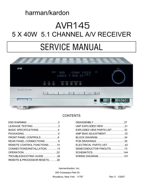
harman/kardon<br />
<strong>AVR145</strong><br />
5 X 40W 5.1 CHANNEL A/V RECEIVER<br />
SERVICE MANUAL<br />
CONTENTS<br />
ESD WARNING……………………………….2<br />
LEAKAGE TESTING……………….…..…....3<br />
BASIC SPECIFICATIONS…………………..4<br />
PACKAGING…………………………….……5<br />
FRONT PANEL CONTROLS………..…..…..6<br />
REAR PANEL CONNECTIONS………….…8<br />
REMOTE CONTROL FUNCTIONS……….10<br />
CONNECTIONS/INSTALLATION………....13<br />
OPERATION………………………...………22<br />
TROUBLESHOOTING GUIDE…...……..…26<br />
REMOTE & PROCESSOR RESETS……....26<br />
DISASSEMBLY……………………………….27<br />
UNIT EXPLODED VIEW…………..…….…..31<br />
EXPLODED VIEW PARTS LIST……………32<br />
AMP BIAS ADJUSTMENT……………….…33<br />
BLOCK DIAGRAM…………………………..34<br />
PCB DRAWINGS……………………………35<br />
ELECTRICAL PARTS LIST………..….……42<br />
SEMICONDUCTOR PINOUTS…….………73<br />
SCHEMATICS………………………………144<br />
WIRING DIAGRAM…………………………151<br />
harman/kardon, Inc.<br />
250 Crossways Park Dr.<br />
Woodbury, New York 11797 Rev 0 1/2007
<strong>AVR145</strong><br />
harman/kardon<br />
Some semiconductor (solid state) devices can be damaged easily by static electricity. Such components commonly are called<br />
Electrostatically Sensitive (ES) Devices. Examples of typical ES devices are integrated circuits and some field effect transistors and<br />
semiconductor "chip" components.<br />
The following techniques should be used to help reduce the incidence of component damage caused by static electricity.<br />
1. Immediately before handling any semiconductor component or semiconductor-equipped assembly, drain off any electrostatic charge on<br />
your body by touching a known earth ground. Alternatively, obtain and wear a commercially available discharging wrist strap device,<br />
which should be removed for potential shock reasons prior to applying power to the unit under test.<br />
2. After removing an electrical assembly equipped with ES devices, place the assembly on a conductive surface such as aluminum foil, to<br />
prevent electrostatic charge build-up or exposure of the assembly.<br />
3. Use only a grounded-tip soldering iron to solder or unsolder ES devices.<br />
4. Use only an anti-static solder removal device. Some solder removal devices not classified as "anti-static" can generate electrical charges<br />
sufficient to damage ES devices.<br />
5. Do not use freon-propelled chemicals. These can generate electrical change sufficient to damage ES devices.<br />
6. Do not remove a replacement ES device from its protective package until immediately before you are ready to install it. (Most replacement<br />
ES devices are packaged with leads electrically shorted together by conductive foam, aluminum foil or comparable conductive material.)<br />
7. Immediately before removing the protective material from the leads of a replacement ES device, touch the protective material to the<br />
chassis or circuit assembly into which the device will be installed.<br />
CAUTION : Be sure no power is applied to the chassis or circuit, and observe all other safety precautions.<br />
8. Minimize bodily motions when handling unpackaged replacement ES devices. (Otherwise harmless motion such as the brushing together<br />
or your clothes fabric or the lifting of your foot from a carpeted floor can generate static electricity sufficient to damage an ES devices.<br />
Each precaution in this manual should be followed during servicing.<br />
Components identified with the IEC symbol<br />
in the parts list are special significance to safety. When replacing a component identified with<br />
, use only the replacement parts designated, or parts with the same ratings or resistance, wattage, or voltage that are designated in the<br />
parts list in this manual. Leakage-current or resistance measurements must be made to determine that exposed parts are acceptably<br />
insulated from the supply circuit before retuming the product to the customer.
<strong>AVR145</strong><br />
harman/kardon<br />
SAFETY PRECAUTIONS<br />
The following check should be performed for the continued<br />
protection of the customer and service technician.<br />
LEAKAGE CURRENT CHECK<br />
Measure leakage current to a known earth ground (water<br />
pipe, conduit, etc.) by connecting a leakage current tester<br />
between the earth ground and all exposed metal parts of the<br />
appliance (input/output terminals, screwheads, metal<br />
overlays, control shaft, etc.). Plug the AC line cord of the<br />
appliance directly into a 120V AC 60Hz outlet and turn the<br />
AC power switch on. Any current measured must not exceed<br />
o.5mA.<br />
Device<br />
under<br />
test<br />
Leakage<br />
current<br />
tester<br />
Reading should<br />
not be above<br />
0.5mA<br />
Test all<br />
exposed metal<br />
surfaces<br />
Also test with<br />
plug reversed<br />
(Using AC adapter<br />
plug as required)<br />
Earth<br />
ground<br />
AC Leakage Test<br />
ANY MEASUREMENTS NOT WITHIN THE LIMITS<br />
OUTLINED ABOVE ARE INDICATIVE OF A<br />
POTENTIAL SHOCK HAZARD AND MUST BE<br />
CORRECTED BEFORE RETURNING THE APPLIANCE<br />
TO THE CUSTOMER.<br />
3
<strong>AVR145</strong><br />
harman/kardon<br />
AVR 145 TECHNICAL SPECIFICATIONS<br />
Audio Section<br />
Stereo Mode<br />
Continuous Average Power (FTC)<br />
50 Watts per channel, 20Hz–20kHz,<br />
@
<strong>AVR145</strong><br />
<br />
harman/kardon<br />
<br />
<br />
<br />
<br />
<br />
<br />
<br />
<br />
<br />
<br />
<br />
<br />
<br />
<br />
<br />
<br />
<br />
<br />
<br />
<br />
<br />
AVR 145<br />
<br />
<br />
<br />
<br />
<br />
<br />
<br />
<br />
<br />
<br />
<br />
<br />
<br />
<br />
<br />
<br />
<br />
<br />
<br />
<br />
<br />
<br />
<br />
<br />
<br />
<br />
<br />
<br />
<br />
<br />
<br />
<br />
<br />
<br />
<br />
<br />
<br />
<br />
<br />
<br />
<br />
<br />
<br />
DOOR KIT<br />
<br />
<br />
<br />
<br />
<br />
<br />
<br />
<br />
<br />
<br />
<br />
FRONT COVER "A", SILVER<br />
FRONT COVER "B", SILVER<br />
<br />
<br />
<br />
<br />
<br />
<br />
<br />
<br />
<br />
<br />
<br />
<br />
<br />
<br />
<br />
<br />
<br />
<br />
<br />
<br />
<br />
<br />
<br />
<br />
<br />
<br />
<br />
<br />
<br />
<br />
<br />
5
<strong>AVR145</strong><br />
harman/kardon<br />
FRONT-PANEL CONTROLS<br />
Main Power Switch: This is a mechanical switch that turns the<br />
power supply on or off. It is usually left pressed in (On position) at all<br />
times, and cannot be turned on using the remote control.<br />
Standby/On Switch: This is an electrical switch that turns the<br />
receiver on for playback, or leaves it in standby mode for quick turn-on<br />
using this switch or the remote control.<br />
Power Indicator: This LED has three possible modes. When main<br />
power is turned off, the LED is dark and the receiver won’t respond to<br />
any button presses. When main power is turned on, but before the<br />
Standby/On Switch is used, the LED turns amber and the receiver is<br />
ready to be turned on. When the receiver is turned on, the LED<br />
turns blue.<br />
Source Select: Press this button to select a source device, which is<br />
a component where a playback signal originates, e.g. DVD, CD, cable TV,<br />
satellite or HDTV tuner.<br />
Source Indicators: The name of the current source input lights up.<br />
The indicated input changes each time the Source Select button is<br />
pressed.<br />
Volume Knob: Turn this knob to raise or lower the volume, which will<br />
be shown in decibels (dB) in the Message Display.<br />
Message Display: Various messages appear in this two-line display<br />
in response to commands. When the on-screen display menu system<br />
(OSD) is in use, the message OSD ON will appear to remind you to<br />
check the video display.<br />
Tuner Band: Press this button to select the tuner as the source, or to<br />
switch between the AM and FM bands.<br />
Tuning: Press either side of this button to tune a radio station.<br />
Tuning Mode: This button toggles between manual (one frequency<br />
step at a time) and automatic (seeks frequencies with acceptable signal<br />
strength) tuning mode. It also toggles between stereo and mono modes<br />
when an FM station is tuned.<br />
Preset Stations: Press this button to select a preset radio station.<br />
Headphone Jack: Plug a 1/4" headphone plug into this jack for<br />
private listening.<br />
Surround Mode: Press this button to select a type of surround<br />
sound (e.g. multichannel) mode. Choose from the Dolby modes, DTS<br />
modes, Logic 7 modes, DSP modes or Stereo modes.<br />
Surround Select: After you have selected the desired type of surround<br />
mode, press this button to select a specific variant of that type<br />
of mode.<br />
Surround Mode Indicators: One or more of these icons may light<br />
up as you select different surround modes. The Message Display also<br />
indicates the surround mode.<br />
Analog Audio, Video and Digital Audio Inputs: Connect a<br />
source component that will only be used temporarily to these jacks,<br />
such as a camera or game console. Remember to select only one type<br />
of audio and one type of video connection.<br />
Speaker/Channel Input Indicators: The box icons indicate<br />
which speaker positions you have configured, and the size (frequency<br />
range) of each speaker. When a digital audio input is used, letters will<br />
light inside the boxes to indicate which channels are present in the<br />
incoming signal.<br />
Navigation: These buttons are used together with the following five<br />
buttons to make selections.<br />
Tone Mode: Press this button to access the tone controls (bass and<br />
treble). Use the ‹/› Navigation buttons to make your selections.<br />
Speaker: Press this button to configure speaker sizes, that is, the frequency-range<br />
capability of each speaker.<br />
Channel Level Adjust: Press this button to set the output levels for<br />
each channel so that all speakers sound equally loud at the listening<br />
position.<br />
Digital Input Select: Press this button to select the specific digital<br />
audio input (or analog audio input) you used for the current source.<br />
Delay: Press this button to set delay times that compensate for placing<br />
the speakers at different distances from the listening position.<br />
6<br />
7
<strong>AVR145</strong> harman/kardon<br />
Channel Level<br />
Adjust<br />
Speaker Size Tone Mode<br />
Setup<br />
Navigation Surround Mode Indicators<br />
Message Display<br />
Speaker/Channel<br />
Input Indicators<br />
Source<br />
Indicators<br />
Delay<br />
Digital Input<br />
Select<br />
Volume<br />
Standby/On<br />
Switch<br />
Power<br />
Indicator<br />
Main Power<br />
Switch<br />
Surround<br />
Mode<br />
Surround<br />
Select<br />
Tuning<br />
Tuner Band<br />
Preset Stations<br />
Source<br />
Select<br />
Headphone<br />
Jack<br />
Tuning<br />
Mode<br />
Digital<br />
Audio Inputs<br />
Video Inputs<br />
Analog Audio<br />
Inputs<br />
NOTE: To make it easier to follow the instructions throughout the manual that refer to this illustration, a copy of this page may be downloaded from the Product Support section at<br />
www.harmankardon.com<br />
7
<strong>AVR145</strong><br />
harman/kardon<br />
REAR-PANEL CONNECTIONS<br />
AM and FM Antenna Terminals: Connect the included AM and<br />
FM antennas to their respective terminals for radio reception.<br />
Front, Center and Surround Speaker Outputs: Use two-conductor<br />
speaker wire to connect each set of terminals to the correct<br />
speaker. Remember to observe the correct polarity (positive and negative<br />
connections). Always connect the positive lead to the colored terminal<br />
on the receiver and the red terminal on the speaker. Connect the<br />
negative lead to the black terminal on both the receiver and the speaker.<br />
See the Connections section for more information on connecting your<br />
speakers.<br />
Subwoofer Output: If you have a powered subwoofer, connect it to<br />
this jack.<br />
Video 1, Video 2 and DVD Audio/Video Inputs: These jacks<br />
may be used to connect your video-capable source components (e.g.,<br />
VCR, DVD player, cable TV box) to the receiver. Remember to use only<br />
one type of video connection for each source. See the Connections<br />
section for more information on audio and video connection options for<br />
each source component.<br />
Video 1 Audio/Video Outputs: These jacks may be used to connect<br />
your VCR or another recorder.<br />
Composite and S-Video Monitor Outputs: If some of your<br />
sources use composite or S-video connections, then you will need to<br />
connect one or both of these monitor outputs to the corresponding<br />
inputs on your television or video display in order to view the sources.<br />
CD and Tape Audio Inputs: These jacks may be used to connect<br />
your audio-only source components (e.g., CD player, tape deck). Do not<br />
connect a turntable to these jacks unless you are using the turntable<br />
with a phono preamp.<br />
Tape Outputs: These jacks may be used to connect your CDR or<br />
another audio-only recorder.<br />
Coaxial and Optical Digital Audio Inputs: If your source has<br />
a compatible digital audio output, connect it to one of these jacks for<br />
improved audio performance. Remember to use only one type of digital<br />
audio connection for each source.<br />
Coaxial and Optical Digital Audio Outputs: If your source is<br />
also an audio recorder, you may connect a compatible digital audio output<br />
to the recorder’s input for improved recording quality.<br />
The Bridge/DMP Input: Connect the optional <strong>Harman</strong> <strong>Kardon</strong><br />
The<br />
BridgeTM to this input for use with your iPod (not included). Make<br />
sure the receiver is turned off (in Standby mode) when connecting<br />
The Bridge.<br />
6-Channel Inputs: Connect the analog audio outputs of a DVD-<br />
Audio, SACD , Blu-ray Disc or HD-DVD player (or any other external<br />
decoder) to these jacks to enjoy these proprietary formats.<br />
Component Video Inputs: If both your video source (e.g., DVD<br />
player or HDTV tuner) and your television or video display have analog<br />
component video (Y/Pb/Pr) capability, then you may connect the component<br />
video outputs of your source to one of the two component video<br />
inputs. Do not make any other video connections to that source.<br />
Component Video Monitor Outputs: If you are using one or<br />
both of the Component Video Inputs and your television or video display<br />
is component-video-capable, you may connect these jacks to the corresponding<br />
inputs on your video display. You will also need to connect the<br />
composite and/or S-video monitor outputs to your video display if some<br />
of your sources use those types of video connections.<br />
RS-232 Serial Port: This specialized connector may be used with<br />
your personal computer in case <strong>Harman</strong> <strong>Kardon</strong> offers a software<br />
upgrade for the receiver at some time in the future.<br />
RS-232 Mode: Leave this switch popped out in the Operate position<br />
unless the AVR 145 is being upgraded.<br />
RS-232 Reset: This switch is only used during a software upgrade.<br />
A standard processor reset is performed by pressing and holding the<br />
front-panel Tone button.<br />
Switched AC Accessory Outlet: You may plug the AC power<br />
cord of one source device into this outlet, and it will turn on whenever<br />
you turn on the receiver. Do not use a source that consumes more than<br />
50 watts of power.<br />
AC Power Cord: After you have made all other connections, plug the<br />
AC power cord into an unswitched outlet.<br />
8<br />
9
<strong>AVR145</strong> harman/kardon<br />
10<br />
FM Antenna<br />
AM Antenna<br />
Video 2<br />
A/V<br />
Inputs<br />
Video 1<br />
A/V<br />
Outputs<br />
Video 1<br />
A/V<br />
Inputs<br />
DVD A/V<br />
Inputs<br />
Video<br />
Monitor<br />
Outputs<br />
Component Video<br />
Inputs (1 & 2)<br />
Component Video<br />
Monitor Outputs<br />
Coaxial Digital<br />
Audio Inputs<br />
(1 & 2)<br />
The Bridge/<br />
DMP Input<br />
RS-232<br />
Reset<br />
RS-232<br />
Serial Port<br />
RS-232<br />
Mode<br />
AC Power<br />
Cord<br />
CD<br />
Inputs<br />
Tape<br />
Outputs<br />
Tape<br />
Inputs<br />
Subwoofer<br />
Output<br />
Front<br />
Speaker<br />
Outputs<br />
6-Channel<br />
Inputs<br />
Surround<br />
Speaker<br />
Outputs<br />
Center<br />
Speaker<br />
Outputs<br />
Coaxial Digital<br />
Audio Output<br />
Switched AC<br />
Accessory<br />
Outlet<br />
Optical Digital<br />
Audio Output<br />
Optical Digital<br />
Audio Inputs (1 & 2)<br />
NOTE: To make it easier to follow the instructions throughout the manual that refer to this illustration, a copy of this page may be downloaded from the Product Support section at<br />
www.harmankardon.com<br />
9
<strong>AVR145</strong><br />
harman/kardon<br />
REMOTE CONTROL FUNCTIONS<br />
The AVR 145 remote is capable of controlling nine devices, including<br />
the AVR itself and an iPod docked in the optional The Bridge accessory.<br />
During the installation process, you may program the codes for each of<br />
your source components into the remote. Each time you wish to use the<br />
codes for any component, you will need to first press the Selector button<br />
for that component. This changes the button functions to the appropriate<br />
codes for that product.<br />
Each Input Selector has been preprogrammed to control certain types<br />
of components, with only the codes specific to each brand and model<br />
changing, depending on which product code is programmed. The<br />
device types programmed into each selector may not be changed.<br />
DVD: Controls DVD players and recorders.<br />
CD: Controls CD players and recorders.<br />
Tape: Controls cassette decks.<br />
Video 1: Controls VCRs, TiVo and DVRs.<br />
Video 2: Controls cable and satellite television set-top boxes.<br />
Video 3: Controls televisions and other video displays.<br />
The Bridge/DMP: Controls an iPod docked in The Bridge.<br />
For example, if you have inserted a disc in your CD player and Iyou<br />
would like to skip ahead three tracks, but you then find that the volume<br />
is too loud, you would follow this procedure:<br />
1. Press the CD Input Selector to switch to the codes that control your<br />
CD player.<br />
2. Press the Play Button (in the Transport Controls section) if the disc is<br />
not already playing.<br />
3. Press the Skip Up Button three times to advance three tracks.<br />
4. Press the AVR Button so that you can access the Volume Controls.<br />
5. Press the Volume Down Button until the volume level is satisfactory.<br />
Any given button may have different functions, depending on which<br />
component is being controlled. Some buttons are labeled with these<br />
functions. For example, the Sleep and DSP Surround Buttons are<br />
labeled for use as Channel Up/Down Buttons when controlling a television<br />
or cable box. See Table A8 in the appendix for listings of the<br />
different functions for each type of component.<br />
IR Transmitter Lens: As buttons are pressed on the remote,<br />
infrared codes are emitted through this lens. Make sure it is pointing<br />
toward the component being operated.<br />
EzSet Microphone: This microphone “hears” the test tone used<br />
during the EzSet level-setting procedure. Make sure it is pointing toward<br />
the receiver when running EzSet.<br />
Power On Button: Press this button to turn on the AVR or another<br />
device. The Master Power Switch on the AVR 145’s front panel must<br />
first have been switched on.<br />
Mute Button: Press this button to mute the AVR 145’s speaker and<br />
headphones outputs temporarily. To end the muting, press this button<br />
or adjust the volume. Muting is also canceled when the receiver is<br />
turned off.<br />
Program/EzSet Indicator: This LED lights up or flashes in one of<br />
three colors as the remote is programmed with codes, and during the EzSet<br />
procedure.<br />
Power Off Button: Press this button to turn off the AVR 145 or<br />
another device.<br />
AVR Selector: Press this button to switch the remote to the codes<br />
that operate the receiver.<br />
Input Selectors: Press one of these buttons to select a source<br />
device, which is a component where a playback signal originates, e.g.,<br />
DVD, CD, cable TV, satellite or HDTV tuner. This will also turn on the<br />
receiver and switch the remote to the codes that operate the source<br />
device.<br />
AM/FM Button: Press this button to select the tuner as the source,<br />
or to switch between the AM and FM bands.<br />
6-Channel Input Selector: Press this button to select the 6-<br />
Channel Inputs as the audio source. The receiver will use the video input<br />
and remote control codes for the last-selected video source.<br />
EzSet (SPL) Button: Press this button to run the EzSet output-level<br />
calibration procedure. Make sure to point the remote toward the receiver<br />
during EzSet.<br />
The Bridge/DMP Selector: Press this button to select an iPod<br />
docked in the optional The Bridge as the audio source. The remote will<br />
switch to the codes that operate the iPod.<br />
Test Tone: Press this button to activate the test tone for manual output-level<br />
calibration.<br />
TV/Video: This button has no effect on the receiver, but is used to<br />
switch video inputs on some video source components.<br />
Sleep Button: Press this button to activate the sleep timer, which<br />
shuts off the receiver after a programmed period of time of up to<br />
90 minutes.<br />
Volume Controls: Press these buttons to raise or lower the volume,<br />
which will be shown in decibels (dB) in the Message Display.<br />
DSP Surround: Press this button to select a DSP surround mode<br />
(Hall 1, Hall 2, Theater).<br />
On-Screen Display (OSD): Press this button to activate the onscreen<br />
menu system.<br />
Channel Level: Press this button to set the output levels for each<br />
channel so that all speakers sound equally loud at the listening position.<br />
Usually this is done while playing an audio selection, such as a favorite CD,<br />
after you have calibrated the levels using EzSet, as described in the Getting<br />
Started section.<br />
10<br />
11
<strong>AVR145</strong><br />
harman/kardon<br />
REMOTE CONTROL FUNCTIONS<br />
Speaker Setup: Press this button to configure speaker sizes, that is,<br />
the frequency-range capability of each speaker. Usually this is done<br />
using the on-screen menu system, as described in the Getting Started<br />
section.<br />
Navigation and Set Buttons: These buttons are used together to<br />
make selections within the on-screen menu system, or when accessing<br />
the functions of the four buttons surrounding this area of the remote –<br />
Channel Level, Speaker Setup, Digital Input or Delay.<br />
Digital Input Select: Press this button to select the specific digital<br />
audio input (or analog audio input) you used for the current source.<br />
Delay: Press this button to set delay times that compensate for placing<br />
the speakers at different distances from the listening position, or to<br />
resolve a “lip sync” issue that may be caused by digital video processing.<br />
This is done using the on-screen menu system, as described in the<br />
Initial Setup section.<br />
Numeric Keys: Use these buttons to enter radio station frequencies<br />
when using the tuner (after pressing the Direct Button), or to select station<br />
presets.<br />
Tuning Mode: This button toggles between manual (one frequency<br />
step at a time) and automatic (seeks frequencies with acceptable signal<br />
strength) tuning mode. It also toggles between stereo and mono modes<br />
when an FM station is tuned.<br />
Memory: After you have tuned a particular radio station, press this<br />
button, then the numeric keys, to save that station as a radio preset.<br />
Tuning: Press these buttons to tune a radio station. Depending on<br />
whether the tuning mode has been set to manual or automatic, each<br />
press will either change one frequency step at a time, or seek the next<br />
frequency with acceptable signal strength.<br />
Direct: Press this button before using the Numeric Keys to directly<br />
enter a radio station frequency.<br />
Clear: Press this button to clear a radio station frequency you have<br />
started to enter.<br />
Preset Stations Selector: Press these buttons to select a preset<br />
radio station.<br />
Tone Mode: Press this button to access the tone controls (bass and<br />
treble). Use the Navigation buttons to make your selections.<br />
Disc Skip: This button has no effect on the receiver, but is used with<br />
some optical disc changers to skip to the next disc.<br />
Macros: These buttons may be programmed to execute long command<br />
sequences with a single button press. They are useful for programming<br />
the command to turn on or off all of your components, or for<br />
accessing specialized functions for a different component than you are<br />
currently operating.<br />
Surround Mode Selectors: Press any of these buttons to select<br />
a type of surround sound (e.g., multichannel) mode. Choose from the<br />
Dolby modes, DTS modes, Logic 7 modes or Stereo modes. Each<br />
press of a button will cycle to the next available variant of that mode.<br />
Not all modes or mode groups are available with all sources.<br />
Night Mode: Press this button to activate Night mode with specially<br />
encoded Dolby Digital discs or broadcasts. Night mode compresses the<br />
audio so that louder passages are reduced in volume to avoid disturbing<br />
others, while dialogue remains intelligible.<br />
Track Skip: These buttons have no effect on the receiver, but are<br />
used with many source components to change tracks or chapters.<br />
Dim: Press this button to partially or fully dim the front-panel display.<br />
Transport Controls: These buttons have no effect on the receiver,<br />
but are used to control many source components. By default, when the<br />
remote is operating the receiver, these buttons will control a DVD player.<br />
11<br />
13
<strong>AVR145</strong><br />
harman/kardon<br />
IR Transmitter Lens<br />
Power On<br />
Program/EzSet Indicator<br />
AVR Selector<br />
AM/FM<br />
EzSet (SPL)<br />
Test Tone<br />
Sleep<br />
DSP Surround<br />
On-Screen Display<br />
Channel Level<br />
EzSet Microphone<br />
Mute<br />
Power Off<br />
Input Selectors<br />
6-Channel Input Selector<br />
The<br />
BridgeTM<br />
/DMP Selector<br />
TV/Video<br />
Volume Control<br />
Not Used<br />
Speaker Setup<br />
Digital Input<br />
Set<br />
Delay<br />
Numeric Keys<br />
Tuning Mode<br />
Direct Station Entry<br />
Tuning<br />
Tone Mode<br />
Night Mode<br />
Track Skip<br />
Transport Controls<br />
Memory<br />
Clear<br />
Preset Stations Selectors<br />
Disc Skip<br />
Macros<br />
Surround Mode Selectors<br />
Dim<br />
145<br />
NOTE: To make it easier to follow the instructions<br />
throughout the manual that refer to this<br />
illustration, a copy of this page may be downloaded<br />
from the Product Support section at<br />
www.harmankardon.com<br />
12
<strong>AVR145</strong><br />
harman/kardon<br />
CONNECTIONS<br />
There are different types of audio and video connections used to connect<br />
the receiver to the speakers and video display, and to connect<br />
the source devices to the receiver. To make it easier to keep them all<br />
straight, the Consumer Electronics Association (CEA) has established a<br />
color-coding standard. Table 1 may be helpful to you as a reference<br />
while you set up your system.<br />
Audio Connections<br />
Front (FL/FR)<br />
Center (C)<br />
Surround (SL/SR)<br />
Subwoofer (SUB)<br />
Surround Back (SBL/SBR)<br />
Digital Audio Connections<br />
Coaxial<br />
Optical Input Output<br />
Video Connections<br />
Component Y Pb Pr<br />
Composite<br />
S-Video<br />
Table 1– Connection Color Guide<br />
Types of Cables<br />
This section will briefly review different types of cables and connections<br />
that you may use to set up your system.<br />
Speaker Cables<br />
Speaker cables carry an amplified signal from the receiver’s speaker terminals<br />
to each loudspeaker. Speaker cables generally contain two wire<br />
conductors, or leads, inside plastic insulation. The two conductors are<br />
usually differentiated in some way, by using different colors, or stripes, or<br />
even by adding a ridge to the insulation. Sometimes the actual wires are<br />
different, one being copper red and the other silver.<br />
The differentiation is important because each speaker must be connected<br />
to the receiver’s speaker-output terminals using two wires, one positive<br />
(+) and one negative (–). This is called speaker polarity. It’s important<br />
to maintain the proper polarity for all speakers in the system. If<br />
some speakers have their negative terminals connected to the receiver’s<br />
positive terminals, performance can suffer, especially for the low frequencies.<br />
Always connect the positive terminal on the loudspeaker, which is usually<br />
colored red, to the positive terminal on the receiver, which is colored as<br />
shown in the Connection Color Guide (Table 1). Similarly, always connect<br />
the black negative terminal on the speaker to the black negative<br />
terminal on the receiver.<br />
+<br />
Left<br />
Right<br />
The AVR 145 uses binding-post speaker<br />
terminals that can accept banana plugs<br />
or bare-wire cables.<br />
Banana plugs are simply plugged into the<br />
hole in the middle of the terminal cap.<br />
Bare wire cables are installed as follows:<br />
1. Unscrew the terminal cap until the pass-through hole in the collar is<br />
revealed.<br />
2. Insert the bare end of the wire into the hole.<br />
3. Screw the cap back into place until the wire is held snugly.<br />
1 2 3<br />
Figure 2 – Binding-Post Speaker Terminals With Bare Wires<br />
Subwoofer<br />
The subwoofer is a specialized type of loudspeaker that is usually connected<br />
in a different way. The subwoofer is used to play only the low<br />
frequencies (bass), which require much more power than the other<br />
speaker channels. In order to obtain the best results, most speaker<br />
manufacturers offer powered subwoofers, in which the speaker contains<br />
its own amplifier on board. Sometimes the subwoofer is connected to<br />
the receiver using the front left and right speaker outputs, and then the<br />
front left and right speakers are connected to terminals on the subwoofer.<br />
More often, a line-level (nonamplified) connection is made<br />
from the receiver’s Subwoofer Output to a corresponding jack on the<br />
subwoofer.<br />
Although the subwoofer output looks similar to the analog audio jacks<br />
used for the various components, it is filtered and only allows the low<br />
frequencies to pass. Don’t connect this output to your other devices.<br />
Although doing so won’t cause any harm, performance will suffer.<br />
Figure 3 – Subwoofer<br />
Pre-out<br />
Subwoofer<br />
Connecting Source Devices to the AVR<br />
The AVR 145 is designed to process audio and video input signals,<br />
playing back the audio and displaying the video on a television or monitor<br />
connected to the AVR. These signals originate in what are known as<br />
“source devices,” including your DVD player, CD player, DVR (digital<br />
video recorder) or other recorder, tape deck, game console, cable or<br />
satellite television box or MP3 player. Although the tuner is built into the<br />
AVR, it also counts as a source, even though no external connections<br />
are needed, other than the FM and AM antennas.<br />
In general, separate connections are required for the audio and video<br />
portions of the signal. The types of connections used depend upon<br />
what’s available on the source device, and for video signals, the capabilities<br />
of your video display.<br />
Figure 1 – Binding-Post Speaker<br />
Terminals With Banana Plugs<br />
15<br />
13
<strong>AVR145</strong><br />
CONNECTIONS<br />
harman/kardon<br />
Audio Connections<br />
There are two formats for audio connections: digital and analog. Digital<br />
audio signals are of higher quality, and are required for listening to<br />
sources encoded with digital surround modes, such as Dolby Digital and<br />
DTS. There are two types of digital audio connections commonly used:<br />
coaxial and optical. Either type of digital audio connection may be used<br />
for each source device, but never both simultaneously for the same<br />
source. However, it’s okay to make both analog and digital audio connections<br />
at the same time to the same source.<br />
Digital Audio<br />
Coaxial digital audio jacks are usually color-coded in orange. Although<br />
they look similar to analog jacks, they should not be confused, and you<br />
should not connect coaxial digital audio outputs to analog inputs or<br />
vice versa.<br />
Coaxial digital<br />
audio cable<br />
Figure 4 – Coaxial Digital Audio<br />
Optical digital audio connectors are normally covered by a shutter to<br />
protect them from dust. The shutter opens as the cable is inserted. Input<br />
connectors are color-coded using a black shutter, while outputs use a<br />
gray shutter.<br />
Optical digital<br />
audio cable<br />
Figure 5 – Optical Digital Audio<br />
Due to the nature of digital signals as binary bits, they aren’t subject<br />
to signal degradation the way analog signals are. Therefore, the quality<br />
of coaxial and optical digital audio connections should be the same,<br />
although it is important to limit the length of the cable. Whichever type of<br />
connection you choose, <strong>Harman</strong> <strong>Kardon</strong> recommends that you always<br />
select the highest quality cables available within your budget.<br />
Analog Audio<br />
Coaxial<br />
Optical<br />
Analog connections require two cables, one for the left channel (white)<br />
and one for the right channel (red). These two cables are often attached<br />
to each other for most of their length. Most sources that have digital<br />
audio jacks also have analog audio jacks, although some older types of<br />
sources, such as tape decks, have only analog jacks. For sources that<br />
are capable of both digital and analog audio, you may wish to make<br />
both connections. If you wish to record materials from DVDs or other<br />
copy-protected sources, you may only be able to do so using analog<br />
connections. Remember to comply with all laws regarding copyright if<br />
you choose to make a copy for your own personal use.<br />
Multichannel analog connections are used with advanced sources where<br />
the digital content is copy-protected and all surround processing is performed<br />
inside the source. These types of connections are usually used<br />
with DVD-Audio, SACD, Blu-ray Disc, HD-DVD and other advanced<br />
players.<br />
Multichannel<br />
analog audio<br />
cable (RCA)<br />
Figure 7 – Multichannel Analog Audio<br />
Figure 8 – The Bridge<br />
<strong>Harman</strong> <strong>Kardon</strong> receivers also include a proprietary, dedicated audio<br />
connection called “The Bridge/DMP”. If you own an iPod with a dock<br />
connector, you may separately purchase The Bridge and connect it to<br />
The Bridge/DMP port on the receiver. Dock your iPod (not included) in<br />
The Bridge, and you may listen to your materials through your high-performance<br />
audio system. You may even use the AVR 145 remote to<br />
control the iPod, with navigation messages displayed on the front panel<br />
and on the screen of a video display connected to the AVR.<br />
Video Connections<br />
Although some sources produce an audio signal only (e.g., CD player,<br />
tape deck), many sources output both audio and video signals (e.g.,<br />
DVD player, cable television box, HDTV tuner, satellite box, VCR, DVR).<br />
In addition to the audio connection, you will need to connect one type of<br />
video connection for each source (never more than one at the same<br />
time for any source).<br />
There are three types of analog video connections: composite video,<br />
S-video and component video.<br />
Composite video is the basic connection most commonly available. The<br />
jack is usually color-coded yellow, and looks like an analog audio jack,<br />
although it is important never to confuse the two. Do not connect a<br />
composite video jack to an analog or coaxial digital audio jack, and vice<br />
versa. Both the chrominance (color) and luminance (intensity) components<br />
of the video signal are transmitted using a single cable.<br />
Composite<br />
video cable<br />
Figure 9 – Composite Video<br />
Front Surround Center<br />
Subwoofer<br />
Analog audio<br />
cable (RCA)<br />
Figure 6 – Analog Audio<br />
L<br />
R<br />
16<br />
14
<strong>AVR145</strong><br />
harman/kardon<br />
CONNECTIONS<br />
S-video, or “separate” video, transmits the chrominance and luminance<br />
components using separate wires contained within a single cable. The<br />
plug on an S-video cable contains four metal pins, plus a plastic guide<br />
pin. Be careful to line up the plug correctly when you insert it into the<br />
jack on the receiver, source or video display.<br />
Composite<br />
video cable<br />
Figure 10 – S-Video<br />
Component video separates the video signal into three components –<br />
one luminance (“Y”) and two subsampled color signals (“Pb” and “Pr”) –<br />
that are transmitted using three separate cables. The “Y” cable is colorcoded<br />
green, the “Pb” cable is colored blue and the “Pr” cable is colored<br />
red.<br />
Component<br />
video cable<br />
Figure 11 – Component Video<br />
If it’s available on your video display, component video is recommended<br />
as the best quality connection, followed by S-video and then<br />
composite video.<br />
Antennas<br />
The AVR 145 uses separate terminals for the included FM and AM<br />
antennas that provide proper reception for the tuner.<br />
The FM antenna uses a 75-ohm F-connector.<br />
Figure 12 – FM Antenna<br />
The AM loop antenna needs to be assembled. Then connect the two<br />
leads to the screw terminals on the receiver.<br />
Figure 13 – AM Antenna<br />
RS-232 Serial Port<br />
The RS-232 serial port on the AVR 145 is used only for data. If<br />
<strong>Harman</strong> <strong>Kardon</strong> releases a software upgrade for the receiver’s operating<br />
system at some time in the future, the upgrade may be downloaded<br />
to the AVR using this port. Complete instructions will be provided at<br />
that time.<br />
15<br />
17
<strong>AVR145</strong><br />
harman/kardon<br />
INSTALLATION<br />
You are now ready to connect your various components to your receiver.<br />
Before beginning, make sure that all components, including the AVR 145,<br />
are turned completely off and their power cords are unplugged. Don’t<br />
plug any of the power cords back in until you have finished<br />
making all of your connections.<br />
Remember that your receiver generates heat while it is playing. Select a<br />
location that leaves several inches of space on all sides of the receiver. It<br />
is preferable to avoid completely enclosing the receiver inside a cabinet.<br />
It is also preferable to stack components on separate shelves rather<br />
than directly on top of the receiver. Some surface finishes are delicate.<br />
Try to select a location with a sturdy surface finish.<br />
Step Three – Connect the Antennas<br />
Connect the FM and AM antennas to their terminals.<br />
AVR 145<br />
Step One – Connect the Speakers<br />
If you have not yet done so, place your speakers in the listening room<br />
as described in the Speaker Placement section above.<br />
Connect the center, front left, front right, surround left and surround right<br />
loudspeakers to the corresponding speaker terminals on the AVR 145.<br />
Remember to maintain the proper polarity by always connecting the<br />
positive and negative terminals on each speaker to the positive and<br />
negative terminals on the receiver. Use the Connection Color Guide<br />
on page 15 as a reference.<br />
Figure 15 – Speaker Connections<br />
Step Two – Connect the Subwoofer<br />
Connect the Subwoofer Output on the AVR 145 to the line-level input on<br />
your subwoofer. Consult the manufacturer’s guide for the subwoofer for<br />
additional information.<br />
AVR 145<br />
AVR 145<br />
FR FL SR SL<br />
Figure 16 – Subwoofer Connection<br />
SUB<br />
AVR 145<br />
C<br />
FM<br />
Figure 17 – Antenna Connections<br />
AM<br />
Step Four – Connect the Source Components<br />
Use the worksheets in the Appendix to note which connections you will<br />
use for each of your source devices.<br />
For each source, select a source input (Video 1, Video 2, Video 3, etc.).<br />
In Table 2 we recommend connecting certain types of sources to certain<br />
source inputs to make it easier to program and use the remote control.<br />
Decide which audio connections you will use. If your source device has<br />
them, use either the coaxial digital or the optical digital audio connection.<br />
Referring to Table 2, we recommend you connect the DVD source<br />
to the Coaxial 1 input jack, and the source designated Video 2 to the<br />
Optical 2 input jack. However, you may make whatever connections are<br />
best for your system.<br />
In addition to the digital audio connections, we recommend that you<br />
connect the analog audio connections for each source, as a backup to<br />
the digital connections. For sources that don’t have digital audio outputs,<br />
you must use the analog audio connections.<br />
For each video source, select one type of video connection. Component<br />
video is preferred, but both your source device and your video display<br />
must have this type of video capability. If either device does not, then<br />
use S-video. Again, if either your source device or your video display<br />
doesn’t have S-video connections, then use composite video.<br />
Referring to Table 2, we recommend that you connect the DVD source<br />
to the Component Video 1 inputs, and any one source designated as<br />
Video 1, Video 2 or Video 3 to the Component Video 2 inputs. However,<br />
you may make whatever video connections are best for your system.<br />
16<br />
19
<strong>AVR145</strong><br />
INSTALLATION<br />
harman/kardon<br />
NOTE: It’s possible for a source to use none of the connections<br />
named for that source. For example, you might connect your<br />
DVD player to the Component Video 1 inputs and the Coax 1<br />
digital audio input. However, we will refer to this source as<br />
“DVD”, and in Step Five of the Initial Setup section you will program<br />
the receiver so that these connections are assigned to the<br />
DVD source. When you select “DVD” as your source using the<br />
front panel or the remote, the correct connections for your DVD<br />
player will be used.<br />
We recommend connecting your various sources using the connections<br />
shown in Table 2 below in order to simplify programming your receiver<br />
and remote control. However, you may connect any device to any<br />
source input.<br />
Device Type AVR 145 Source Input Audio Connections Video Connections<br />
VCR, DVR, PVR, Video 1 • Video 1 Analog (inputs and outputs) • One of component Video 2, Video 1 S-video<br />
TiVo or other and or Video 1 composite video<br />
audio/video recorder • Either Coax 2 or Optical 2, with • For recording, use Video 1 S-video or<br />
corresponding coax or optical digital composite video output, and do not use<br />
output<br />
component video connections at all<br />
Cable TV, Satellite, Video 2 • Video 2 Analog and • One of component Video 2, Video 2<br />
HDTV or other • Optical 1 S-video, Video 2 composite video<br />
device that delivers<br />
television programs<br />
TV, game console, Video 3 (front-panel jacks) • Video 3 Analog and • One of component Video 2, Video 3 S-video<br />
camera or other • Either Coax 3 or Optical 3 or Video 3 composite video<br />
audio/video device<br />
DVD Audio/Video, DVD • DVD Analog • Component Video 1<br />
SACD HD-DVD,<br />
• 6-Channel inputs (optional) and<br />
Blu-ray Disc • Coax 1<br />
CD player CD • CD Analog and • Not required<br />
• Either Coax 2 or Optical 2<br />
CDR, MiniDisc, Tape • Tape Analog (inputs and outputs) and • Not required<br />
cassette • Either Coax 2 or Optical 2<br />
• Use corresponding coax or<br />
optical digital output<br />
Table 2 – Recommended Source Component Connections<br />
Video 1 Source<br />
Since this source includes audio and video recording output jacks, it is<br />
best suited to a video recorder, such as your VCR or DVR.<br />
Referring to Table 2, connect your recorder to the Video 1 Analog Audio<br />
inputs and outputs and to either the Coax 2 or Optical 2 digital audio<br />
input (and corresponding digital audio output). Use either the Video 1<br />
S-video or composite video input and output if you wish to make<br />
recordings. If you don’t plan on recording, you may use the Component<br />
Video 2 inputs.<br />
Figure 18 – Video 1 A/V Inputs and Outputs, and Digital Audio Inputs<br />
Remember to connect the audio and video output jacks on your<br />
recorder to the Video 1 or digital audio input jacks on the AVR, and the<br />
audio and video input jacks on your recorder to the Video 1 or digital<br />
audio output jacks on the AVR.<br />
20<br />
17
<strong>AVR145</strong><br />
harman/kardon<br />
INSTALLATION STEPS<br />
NOTE: It isn’t possible to make recordings using component<br />
video connections. Keep this in mind as you connect other<br />
source devices that you may wish to make recordings from.<br />
Video 2 Source<br />
The Video 2 source is used only for playback, never recording. The<br />
AVR 145 remote control is programmed to operate many brands and<br />
models of cable and satellite television devices, and we recommend<br />
connecting your cable or satellite set-top box to this source.<br />
Referring to Table 2, connect your set-top box to the Video 2 Analog<br />
Audio inputs and to the Optical 1 Digital Audio input. If possible, use<br />
the Component Video 2 inputs. Otherwise, connect the set-top box’s<br />
S-video or composite video output to the matching Video 2 video input.<br />
DVD<br />
The DVD source is used for a DVD player. If you have a more advanced<br />
multichannel device, such as a Blu-ray Disc or HD-DVD player, connect<br />
it to the DVD source.<br />
Referring to Table 2, connect your DVD player to the DVD Analog Audio<br />
inputs and to the Coaxial 1 Digital Audio input. If possible, use the<br />
Component Video 1 inputs. Otherwise, connect the DVD player’s S-video<br />
or composite video output to the matching DVD video input.<br />
Figure 21 – DVD A/V, DIgital Audio and Component Video Inputs<br />
If your DVD player plays multichannel lossless discs, such as SACD or<br />
DVD-Audio, you will also need to connect the 6-channel analog audio<br />
outputs on the DVD player to the 6-channel analog audio inputs on the<br />
receiver in order to enjoy these discs to their fullest.<br />
Figure 19 – Video 2 A/V, DIgital Audio and Component Video Inputs<br />
NOTE: If you receive your television programming using your TV<br />
with an antenna or direct cable connection, then you will need<br />
to connect the analog and optical digital audio (if available on<br />
your TV) outputs to the Video 2 Analog Audio inputs and to the<br />
Optical 1 Digital Audio input. Do not connect any video output<br />
on the television set to any video input on the receiver. See<br />
Step Five for information on connecting the receiver’s video<br />
monitor outputs to the television.<br />
Video 3 Source<br />
The Video 3 source is used only for playback, never recording. It is also<br />
generally reserved for components that are only temporarily connected<br />
to the receiver, such as cameras and game consoles. When not in use,<br />
you may place the supplied covers over the front-panel Video 3 jacks<br />
for a cleaner appearance. Simply snap the covers in place. When you<br />
wish to use the jacks, gently press on the left side of each cover to pivot<br />
it out for removal.<br />
Referring to Table 2, connect your camera or game console to the<br />
Video 3 Analog Audio inputs and to either the Coaxial 3 or Optical 3<br />
digital audio input. If possible, use the Component Video 2 inputs.<br />
Otherwise, connect the component’s S-video or composite video<br />
output to the matching Video 3 video input.<br />
Figure 20 – Video 3 A/V and Digital Audio Inputs<br />
Figure 22 – 6-Channel Analog Audio Inputs<br />
CD<br />
The CD source is used for a strictly audio device, such as a CD player.<br />
Referring to Table 2, connect your CD player to the CD Analog Audio<br />
inputs and to the Coaxial 2 or Optical 2 Digital Audio input.<br />
Figure 23 – CD Audio Inputs and Digital Audio Inputs<br />
No video connections are made, although if your system has unusual<br />
requirements, you may connect a video device using component video<br />
outputs to the Component Video 2 inputs on the receiver, if those jacks<br />
are not in use by another device.<br />
Tape<br />
The Tape source is used for audio-only recorders, such as a CDR,<br />
MiniDisc or cassette deck.<br />
Referring to Table 2, connect your recorder to the Tape Analog Audio<br />
inputs and outputs, and to either the Coax 2 or Optical 2 Digital Audio<br />
input (and corresponding digital audio output).<br />
18<br />
21
<strong>AVR145</strong><br />
INSTALLATION<br />
harman/kardon<br />
Figure 26 – Component Video Monitor Outputs<br />
Figure 24 – Tape Audio Inputs and Outputs, and Digital Audio Inputs and Outputs<br />
Remember to connect the output jacks on your recorder to the Tape<br />
or digital audio input jacks on the AVR, and the input jacks on your<br />
recorder to the Tape or digital audio output jacks on the AVR.<br />
No video connections are made, although if your system has unusual<br />
requirements, you may connect a video device using component video<br />
outputs to the component Video 2 inputs on the receiver, if those jacks<br />
are not in use by another device.<br />
The<br />
BridgeTM<br />
With <strong>Harman</strong> <strong>Kardon</strong>’s optional The Bridge, you can listen to audio<br />
stored on your iPod (not included), use your AVR 145 remote<br />
control to operate the iPod, and even charge the iPod while it’s<br />
docked in The Bridge.<br />
Simply plug the proprietary cable from The Bridge into the special<br />
The Bridge/DMP connector on the rear of the AVR 145’s. Refer to the<br />
owner’s manual for The Bridge to select the appropriate insert to<br />
match your iPod.<br />
Figure 25 – The Bridge/DMP Connector<br />
Step Five – Connect Video Display<br />
Only video connections should be made between the receiver and your<br />
video display (TV), unless your TV is the source for your television programming<br />
(see note above).<br />
You will need to make a video connection for each type of video used<br />
for your sources. In addition, even if you didn’t use S-video or composite<br />
video for any of your sources, you will still need to use one of these<br />
two video monitor connections in order to view the AVR 145’s onscreen<br />
menus and displays.<br />
First, determine what types of video your display is capable of handling.<br />
Remember that component video is preferred, followed by S-video and<br />
then composite video. Ideally, this guided you in selecting the video connections<br />
for your sources.<br />
Next, note which types of video connections you used for your source<br />
devices. Make sure you didn’t use a better type of video connection for<br />
a source than your video display can handle. If so, you will need to disconnect<br />
the source and use a video connection that’s compatible with<br />
your display.<br />
If you used component video for any sources, connect the Component<br />
Video Monitor outputs on the receiver to one set of component video<br />
inputs on your display. Make a note of how these inputs are labeled on<br />
the display.<br />
If you used S-video for any sources, or if all of your sources used component<br />
video, connect the S-video Monitor output on the receiver to an<br />
S-video input on your display. Make a note of how the input is labeled.<br />
If you used composite video for any sources, connect the composite<br />
video Monitor output on the receiver to a composite video input on the<br />
display. Again, make a note of how this input is labeled on the display.<br />
Figure 27 – S-Video and Composite Video Monitor Outputs<br />
Consult the manual for your TV to make sure you understand how to<br />
select each video input. As you play different source devices that use<br />
different types of video connections, you will need to remember to<br />
select the correct video input on your video display.<br />
Step Six – Plug in AC Power<br />
Having made all of your wiring connections, it is now time to plug each<br />
component’s AC power cord into a working outlet.<br />
You may plug one device into the AC Switched Accessory Outlet on the<br />
rear of the AVR 145. Make sure this device draws no more than 50<br />
watts. The device should have its mechanical or master power switch<br />
turned on, and it will power on any time the AVR 145 is turned on.<br />
Figure 28 – Switched AC Accesssory Outlet<br />
Before plugging the AVR 145’s AC Power Cord into an electrical outlet,<br />
make sure that the Master Power Switch on the front panel is popped<br />
out so that the word OFF appears on its top. Gently press the button to<br />
turn the switch off. This will prevent the possibility of damaging the AVR<br />
in case of a transient power surge.<br />
Step Seven – Insert Batteries in Remote<br />
The AVR 145 remote control uses three AAA batteries, which are<br />
included.<br />
To remove the battery cover located on the back of the remote, firmly<br />
press the ridged depression and slide the cover towards the top of<br />
the remote.<br />
22<br />
19
<strong>AVR145</strong><br />
harman/kardon<br />
INSTALLATION<br />
Insert the batteries as shown in the diagram, making sure to observe<br />
the correct polarity.<br />
Figure 30 – Input Selectors<br />
Figure 29 – Remote Battery Compartment<br />
When using the remote, remember to point the lens toward the front<br />
panel of the AVR 145. Make sure no objects, such as furniture, are<br />
blocking the remote’s path to the receiver. Bright lights, fluorescent lights<br />
and plasma video displays may interfere with the remote’s functioning.<br />
The remote has a range of about 20 feet, depending on the lighting<br />
conditions. It may be used at an angle of up to 30 degrees to either<br />
side of the AVR.<br />
If the remote seems to operate intermittently, or if pressing a button<br />
on the remote does not cause the AVR Selector or one of the Input<br />
Selectors to light up, then make sure the batteries have been inserted<br />
correctly, or replace all three batteries with fresh ones.<br />
Step Eight – Program Sources Into the Remote<br />
The AVR 145 remote is capable of controlling not only the receiver,<br />
but it may also be programmed to control many brands and models of<br />
VCRs, DVD players, CD players, cable boxes, satellite receivers, cassette<br />
decks and TVs, as well as The Bridge.<br />
It may help to think of the remote as a book with pages. Each page represents<br />
the button functions for a different device. In order to access the<br />
functions for a particular device, you first need to turn to that page. This<br />
is done by pressing the AVR Button to access the codes that control the<br />
receiver, or the Input Selector buttons to access the codes for the<br />
devices programmed into the remote.<br />
At the factory, the AVR 145’s codes and the codes to control an iPod<br />
docked in The Bridge are preprogrammed, and the codes for many<br />
<strong>Harman</strong> <strong>Kardon</strong> DVD and CD players are also preprogrammed. If you<br />
have other source devices in your system, follow these steps to program<br />
the correct codes into the remote.<br />
1. Using the codes in Tables A9–A16 of the Appendix, look up the<br />
product type (e.g. DVD, cable TV box) and the brand name of your<br />
source. The number(s) listed are potential candidates for the correct<br />
code set for your particular device.<br />
2. Turn on your source device.<br />
3. Put the remote into Program mode by pressing and holding the Input<br />
Selector and the Mute button simultaneously until the LED on the<br />
remote starts to flash, and then releasing the buttons.<br />
4. Enter a code from Step 1 above.<br />
a) If the device turns off, then press the Input Selector again to accept<br />
the code, which will flash. The remote will exit the Program mode.<br />
b) If the device does not turn off, try entering another code. If you run<br />
out of codes, you may search through all of the codes in the<br />
remote’s library for that product type by pressing the ⁄ or ¤<br />
button repeatedly until the device turns off. When the device turns<br />
off, enter the code by pressing the Input Selector, which will flash.<br />
The remote then exits Program mode.<br />
5. Once you have accepted a code, it’s a good idea to try using some<br />
other functions to control the device. Sometimes manufacturers<br />
use the same Power code for several different models, while other<br />
codes will vary. You may wish to repeat this process until you’ve programmed<br />
a satisfactory code set that operates most of the functions<br />
you frequently use.<br />
6. You may find out which code number you have programmed by<br />
pressing and holding the Input Selector and Mute Button simultaneously<br />
to enter the Program mode. Then press the Set Button, and the<br />
LED will blink in the code sequence. One blink represents “1”, two<br />
blinks for “2”, and so forth. A series of many fast blinks represents<br />
“0”. Record the codes programmed for each device here.<br />
Source Input Product Type Remote Control Code<br />
(circle one)<br />
Video 1 VCR, PVR<br />
Video 2 Cable, Satellite<br />
Video 3 TV<br />
DVD<br />
DVD<br />
CD<br />
CD, CDR<br />
Tape<br />
Cassette<br />
Table 3 – Remote Control Codes<br />
If you are unable to locate a code set that correctly operates your<br />
source device, it will not be possible to use the AVR remote to control<br />
that device. However, you may still connect the source to the AVR 145<br />
and operate it using the device’s original remote control. Alternatively,<br />
you may wish to consider purchasing <strong>Harman</strong> <strong>Kardon</strong>’s optional TC 30<br />
activity-based remote, which is programmed by accessing a large database<br />
of product codes on the Internet. The TC 30 is also capable of<br />
“learning” codes from your device’s original remote.<br />
20<br />
23
<strong>AVR145</strong><br />
INSTALLATION<br />
harman/kardon<br />
Most of the button labels on the remote describe the button’s function<br />
when used to control the AVR 145. However, the button may perform a<br />
very different function when used to control another device. Refer to the<br />
Remote Control Function List, Table A8 in the Appendix, for a list of<br />
each button’s functions with the various product types.<br />
If you wish, you may program Macros, which are preprogrammed code<br />
sequences that execute many code commands with a single button<br />
press. You may also program “punch-through” codes, which allow the<br />
remote to operate the volume, channel or transport controls of another<br />
device without having to switch the remote to the mode for that device.<br />
See pages 43 through 44 for instructions on these advanced programming<br />
functions.<br />
NOTE: The AVR 145 remote is preprogrammed to operate the<br />
transport controls of <strong>Harman</strong> <strong>Kardon</strong> DVD players when the AVR<br />
or the Video 2 (cable/satellite) or Video 3 (TV) source is selected.<br />
The volume and mute controls operate the AVR when any<br />
device except Tape has been selected. You may change this<br />
punch-through programming at any time.<br />
Step Nine – Turn On the AVR 145<br />
Two steps are required the first time you turn on the AVR 145.<br />
Figure 33 – AVR and Input Selectors<br />
NOTE: Any time you press one of the Input Selectors on the<br />
remote (i.e., DVD, CD, TAPE, VID1, VID2 or VID3), the remote<br />
will switch modes so that it will only transmit the codes programmed<br />
to operate that device. In order to control the receiver,<br />
you will need to press the AVR button to return the remote to<br />
AVR mode.<br />
1. Gently press the Master Power Switch until the word OFF is no longer<br />
visible. The Power Indicator above the two power switches should<br />
light up in amber. This indicates that the AVR is in Standby mode and<br />
is ready to be turned on. Normally, you may leave the Master Power<br />
Switch in the ON position, even when the receiver is not being used.<br />
Figure 31 – Power Switches<br />
2. There are several ways in which the AVR 145 may be turned on from<br />
Standby mode.<br />
a) Press the Standby/On Switch on the front panel.<br />
b) Press the Source Select Button on the front panel.<br />
Figure 32 – Source Select Button<br />
c) Using the remote, press any one of these buttons: AVR, DVD, CD,<br />
TAPE, VID1, VID2, VID3, AM/FM or 6/8CH.<br />
24<br />
21
<strong>AVR145</strong><br />
harman/kardon<br />
OPERATION<br />
Now that you have installed your system components and completed at<br />
least a basic configuration of your receiver, you are ready to begin<br />
enjoying your home theater system.<br />
Turning On the AVR 145<br />
Gently press the Master Power Switch until the word OFF is no longer visible.<br />
The Power Indicator above the two power switches should light up in<br />
amber. This indicates that the AVR is in Standby mode and is ready to be<br />
turned on. Normally, you may leave the Master Power Switch in the ON<br />
position, even when the receiver is not being used.<br />
To turn the receiver off, press either the Standby/On Switch on the front<br />
panel, or press the AVR Button and the OFF Button on the remote.<br />
Unless the receiver will not be used for an extended period of time (for<br />
example, if you will be on vacation), it is not necessary to turn off the<br />
Master Power Switch. When the Master Power Switch is turned off, any<br />
settings you have programmed, including system configuration and preset<br />
radio stations, will be preserved for up to four weeks.<br />
Sleep Timer<br />
You may program the AVR to play for up to 90 minutes and then turn<br />
off automatically using the sleep timer.<br />
Press the Sleep Button on the remote, and the time until turn-off will be<br />
displayed. Each additional press of the Sleep Button will reduce the time<br />
until turn-off by 10 minutes, until the OFF setting is reached, which disables<br />
the sleep timer.<br />
Figure 44 – Power Switches<br />
There are several ways in which the AVR 145 may be turned on:<br />
a) Press the Standby/On Switch on the front panel.<br />
b) Press the Source Select Button on the front panel.<br />
Figure 45 – Source Select Button<br />
c) Using the remote, press any one of these buttons: AVR, DVD, CD,<br />
TAPE, VID1, VID2, VID3, AM/FM, 6/8CH or The Bridge/DMP.<br />
Figure 47 – Sleep Button<br />
When the sleep timer has been set, the front-panel display will automatically<br />
dim to half-brightness. If you press any button on the remote or<br />
front panel, the display will return to full-brightness. The display will dim<br />
again several seconds after your last command.<br />
If you press the Sleep Button after the timer has been set, the remaining<br />
time until turn-off will be displayed. You may press the Sleep Button to<br />
change the time until turn-off. Pressing and holding the Sleep Button will<br />
disable the sleep timer, and the SLEEP OFF message will appear.<br />
Volume Control<br />
The volume may be adjusted either by turning the knob on the front<br />
panel (clockwise to increase volume or counterclockwise to decrease<br />
volume), or by pressing the Volume Control Buttons on the remote. The<br />
volume is displayed as a negative number of decibels (dB) below the<br />
0dB reference point, and may be changed in 0.5dB increments. Unlike<br />
some volume controls on other products, 0dB is the maximum volume<br />
for the AVR 145. Although it’s physically possible to turn the volume to a<br />
higher level, doing so may damage your hearing and your speakers. For<br />
certain more-dynamic audio materials, even 0dB may be too high,<br />
allowing for damage to equipment.<br />
Figure 46 – AVR and Input Selectors<br />
NOTE: Any time you press one of the remote’s Input Selectors<br />
(i.e., DVD, CD, TAPE, VID1, VID2, VID3 or The Bridge/DMP), the<br />
remote will switch modes so that it will only transmit the codes<br />
programmed to operate that device. In order to control the<br />
receiver, you will need to press the AVR Button to return the<br />
remote to AVR mode.<br />
Figure 48 – Volume Controls<br />
22<br />
31
<strong>AVR145</strong><br />
OPERATION<br />
harman/kardon<br />
Remember that the AVR 145 is designed to reproduce audio with a<br />
minimum amount of distortion. This clarity may lead you to think that<br />
your hearing and the equipment can handle higher volumes. We urge<br />
caution with regard to volume levels.<br />
Mute Function<br />
To temporarily mute all speakers and the headphones, press the Mute<br />
Button on the remote. Any recording in progress will not be affected.<br />
The MUTE message will flash in the display as a reminder. To restore<br />
normal audio, either press the Mute Button again, or adjust the volume.<br />
Turning off the AVR will also end muting.<br />
Figure 49 – Mute Button<br />
Tone Controls<br />
You may boost or cut either the treble or the bass frequencies by up<br />
to 10dB in 2dB increments.<br />
Using the front-panel controls or the remote, press the Tone Mode<br />
Button once. This will indicate whether the tone controls are in or out<br />
of the circuitry. If you wish to return the tone controls to 0, or “flat”<br />
response, press the ‹/› Buttons until the TONE OUT message<br />
appears, which preserves any changes you have made to the bass or<br />
treble settings for later use. To reactivate your changes, the tone control<br />
must again be set to TONE IN.<br />
With the TONE IN message displayed, press the Tone Mode Button<br />
repeatedly to access TREBLE MODE and BASS MODE. Use the ‹/›<br />
Buttons to change the treble or bass settings, as desired. The display<br />
will return to normal a few seconds after your last command.<br />
BACK TO MASTER MENU line if you wish to make other changes using<br />
the menu system.<br />
NOTE: The AVR 145 does not have any conventional balance<br />
control. The EzSet process compensates for any characteristics<br />
of your room or speakers, and we recommend that you leave<br />
the settings as they are after EzSet has been run. However, you<br />
may manually adjust the levels of the left and right channels –<br />
decreasing one and increasing the other by the same amount –<br />
using the Channel Adjust submenu, as described on page 41.<br />
This achieves the same effect as a balance control.<br />
Headphones<br />
Plug the 1/4" plug on a pair of headphones into the headphone jack on<br />
the front of the receiver for private listening. The first time you use the<br />
headphones, the DOLBY H:BP message will be displayed, indicating that<br />
Dolby Headphone surround processing is in the bypass mode, which<br />
delivers a conventional 2-channel signal to the headphones.<br />
Figure 51 – Headphone Jack<br />
Press the Surround Select Button on the front panel, or the Dolby<br />
Button on the remote, to switch to Dolby Headphone virtual surround<br />
processing, indicated by the DOLBY H:DH message. Dolby Headphone<br />
delivers an enhanced sound field that emulates a 5.1-channel speaker<br />
system. No other surround modes are available for the headphones.<br />
Source Selection<br />
Press the front-panel Source Select Button to scroll through the<br />
sources. The left side of the button scrolls down the list that appears in<br />
the display; the right side scrolls upward. For direct access to the tuner,<br />
press the Tuner Band Button, which switches to the last-used band and<br />
frequency. For direct access to any source, press its Input Selector on<br />
the remote (see Figure 46).<br />
Figure 50 – Tone Button<br />
You may alternatively adjust the tone controls using the full-OSD menu<br />
system. Press the OSD Button on the remote to view the Master Menu.<br />
The cursor will be pointing to the INPUT SETUP line; press the Set<br />
Button to display that menu. You will be able to view the tone settings. If<br />
you wish to make any changes to the TONE, BASS or TREBLE settings,<br />
use the arrow keys on the remote to move the cursor to the line you<br />
wish to change. Once you have changed the setting using the ‹/›<br />
Buttons, simply move the cursor up or down to a different line; it isn’t<br />
necessary to press the Set Button to enter the new setting. When you<br />
have finished, either wait until the display times out and disappears,<br />
press the OSD Button to clear the display, or move the cursor to the<br />
Figure 52 – Source Select and Tuner Band Buttons<br />
NOTE: The Bridge/DMP source has no icon in the Source<br />
Indicators display. When selected, the DMP indication will<br />
appear in the message display’s upper line, and one of two<br />
messages will scroll on the right side to indicate whether<br />
The Bridge is unplugged or connected. If you have retitled this<br />
source, then only the new name will appear in the upper line.<br />
The AVR 145 will switch to the audio and video inputs assigned to that<br />
source. If you set the BASS MGR setting in the Speaker X-over menu to<br />
32<br />
23
<strong>AVR145</strong><br />
harman/kardon<br />
OPERATION<br />
INDEPENDENT, the AVR 145 will change the speaker size configuration<br />
to the one you programmed for the source. If you selected a surround<br />
mode for the source, the AVR 145 will switch to that mode.<br />
The source name will appear in the upper line of the front-panel display.<br />
If you retitled the source, only the new title will appear. Otherwise, the<br />
audio input assigned to the source (analog or one of the digital audio<br />
inputs) will also appear. The surround mode will be displayed on the<br />
lower line. The same information will also appear on screen in the<br />
semi-OSD, unless you have set the semi-OSD to OFF in the System<br />
Setup menu.<br />
Audio Input Selection<br />
The AVR 145 is programmed at the factory to use the analog audio<br />
inputs for each source (except for the DVD and Video 2 sources, which<br />
default to Coax 1 and Optical 1). To assign a digital audio input to a<br />
source (if you have not done so using the Input Setup menu during<br />
Initial Setup), press the Digital Button on the remote or front panel. The<br />
current audio input selection will flash in the display, and you may press<br />
the ⁄/¤ (or ‹/› on the front panel) Buttons to scroll through the<br />
audio inputs. When the desired input appears, press the Set Button to<br />
select it.<br />
source, it will be selected. If your device is not using component video,<br />
make sure that other devices connected to the component video inputs<br />
are turned off.<br />
If no signal is present at the component video input, then the S-video or<br />
composite video input for the source will be selected. It is not possible<br />
to reassign the S-video or composite video inputs to other sources.<br />
For audio-only sources, such as the tuner or CD inputs, when no<br />
component video signal is present, the last-used video source will be<br />
selected.<br />
6-Channel Direct Inputs<br />
If you wish to hear audio through the 6-Channel Direct Inputs together<br />
with video, then connect your multichannel player to the Component<br />
Video 1 Inputs (the default for the 6-Channel Inputs), and the correct<br />
audio and video inputs will be selected when you select 6CH as your<br />
source. If your multichannel player uses S-video or composite video<br />
connections, you will first need to select the source you connected the<br />
video output to (e.g., DVD), and then select the 6CH source.<br />
Figure 55 – 6-Channel Input Selector<br />
Figure 53 – Digital Input Selection<br />
If the Auto Poll feature has been left ON in the Input Setup menu, and if<br />
a digital audio input has been assigned to the source, the AVR 145 will<br />
first check the digital audio input for a signal. If a signal is present, the<br />
AVR 145 will select the digital audio input. If no signal is present, the<br />
AVR 145 will switch to the analog audio inputs for the source.<br />
Video Input Selection<br />
When a source is selected, the AVR 145 switches to a video input<br />
as follows:<br />
The COMPONENT IN line of the Input Setup menu indicates which<br />
of the two component video inputs on the AVR 145 is assigned to<br />
each source. All of the sources listed in the left column of the Source<br />
Indicators display on the front panel are assigned to the Component<br />
Video 2 inputs by default, and the sources listed in the right column<br />
default to the Component Video 1 sources. This list appears in<br />
Figure 54.<br />
DIGITAL LOGIC 7 VID 1 DVD<br />
PRO LOGIC<br />
VID 2 CD<br />
3 STEREO VID 3 FMAM<br />
DSP<br />
5 7 CH. STEREO<br />
TAPE<br />
SURR. OFF<br />
6 8 CH<br />
NOTE: The 6-Channel Inputs pass the incoming signals directly<br />
to the volume control, without digitizing or processing them.<br />
Therefore, you will need to configure bass management settings<br />
(i.e., speaker size, delay and output level) on your source device<br />
so that they match the settings you programmed using the<br />
Manual Setup menu. Consult the owner’s guide for your multichannel<br />
player for more information.<br />
Using the Tuner<br />
The AVR 145’s built-in tuner may be selected in one of three ways:<br />
1. Press the Source Selector Button on the front panel repeatedly until<br />
the tuner is selected. The last-used band (AM or FM) will be active.<br />
2. Press the Tuner Band Button (marked AM/FM). Press this button<br />
again to switch bands.<br />
3. Press the Tuner Input Selector (marked AM/FM) on the remote. Press<br />
this button again to switch bands.<br />
Figure 54 – Front-Panel Input Indicators<br />
You may reassign either component video input to another source, but<br />
there is no option to disable the component video inputs for any source.<br />
If a signal is present at the component video input assigned to that<br />
Figure 56 – Tuner Input Selection<br />
24<br />
33
<strong>AVR145</strong><br />
OPERATION<br />
harman/kardon<br />
Radio stations may be selected in one of four ways:<br />
1. If you know the frequency number, enter it directly by first pressing<br />
the Direct Button on the remote, and then using the Numeric Keys.<br />
2. After you have programmed Preset stations (see below), either enter<br />
the Preset number (1 through 30) using the remote or use the frontpanel<br />
Preset Stations Button to scroll through the list of presets.<br />
3. In Auto tuning mode, with each press of the Tuning Buttons (frontpanel<br />
or remote) the AVR 145 will scan in the chosen direction until a<br />
station with acceptable signal strength is detected. Press the Tuning<br />
Button again to stop scanning.<br />
4. In Manual tuning mode, with each press of the Tuning Buttons the<br />
AVR 145 will tune the next frequency increment (0.1MHz for FM, or<br />
10kHz for AM) in the selected direction. Press and hold the Tuning<br />
Button for faster scanning.<br />
Figure 57 – Tuning a Station<br />
Press the Tuning Mode Button (TUN-M on the remote) to switch<br />
between Auto and Manual tuning modes. When an FM station has been<br />
tuned, pressing the Tuning Mode Button will switch between stereo and<br />
mono tuning, which may improve reception of weaker stations.<br />
NOTES:<br />
1. Analog audio signals are not converted to digital form, and<br />
digital audio signals are not converted to analog audio form.<br />
However, you may record a coaxial or optical digital audio<br />
source using either type of digital audio output.<br />
Using<br />
2. Only PCM digital audio signals are available for recording.<br />
Proprietary formats such as Dolby Digital and DTS may not<br />
be recorded using the digital audio connections, although if<br />
the source is connected to the AVR using the analog audio<br />
connections, an analog recording may be made.<br />
3. Component video sources are not available for recording.<br />
4. Please make certain that you are aware of any copyright<br />
restrictions on any material you record. Unauthorized duplication<br />
of copyrighted materials is prohibited by federal law.<br />
The<br />
BridgeTM<br />
The Bridge is an optional dock that may be used with a compatible iPod<br />
(not included). When The Bridge is connected to its proprietary input on<br />
the AVR 145 and the iPod is docked, you may play the audio materials<br />
on your iPod through your high-quality audio system, operate the iPod<br />
using the AVR remote or the AVR’s front-panel controls, view navigation<br />
messages on the AVR’s front panel or a connected video display, and<br />
charge the iPod.<br />
Either press the front-panel Source Selector repeatedly until the message<br />
“DMP/The Bridge is CONNECTED” scrolls across the front panel<br />
and semi-OSD displays, or press the DMP Button on the remote to<br />
select The Bridge as the input source.<br />
Figure 58 – Tuning Mode<br />
To store a station in one of the 30 presets:<br />
1. Tune the desired station.<br />
2. Press the Memory Button on the remote.<br />
3. Use the Numeric Keys to enter the desired preset number.<br />
(Left) Figure 60 – Using The Bridge (Remote)<br />
(Above) Figure 61 – Using The Bridge (Front Panel)<br />
Figure 59 – Storing a Preset Station<br />
Recording<br />
Two-channel analog and digital audio signals, as well as composite<br />
and S-video signals, are normally available at the appropriate recording<br />
outputs. Thus, to make a recording, you need only make sure to connect<br />
your audio or video recorder to the appropriate output jacks, as<br />
described in the Installation section, insert blank media and make sure<br />
the recorder is turned on and recording while the source is playing.<br />
34<br />
25
<strong>AVR145</strong><br />
TROUBLESHOOTING GUIDE<br />
SYMPTOM CAUSE SOLUTION<br />
Unit does not function when Main • No AC Power • Make certain AC power cord is plugged into<br />
Power Switch is pushed<br />
a live outlet<br />
• Check to see whether outlet is switch-controlled<br />
Display lights, but no sound • Intermittent input connections • Make certain that all input and speaker connections<br />
or picture<br />
are secure<br />
• Mute is on<br />
• Press Mute Button<br />
• Volume control is down<br />
• Turn up volume control<br />
No sound from any speaker; • Amplifier is in protection mode • Check speaker wire connections for shorts at receiver and<br />
light around power switch is red due to possible short speaker ends<br />
• Amplifier is in protection mode • Contact your local <strong>Harman</strong> <strong>Kardon</strong> service center<br />
due to internal problems<br />
No sound from surround or • Incorrect surround mode • Select a mode other than Stereo<br />
center speakers • Input is monaural • There is no surround information from mono sources<br />
• Incorrect configuration<br />
• Check speaker mode configuration<br />
• Stereo or Mono program material • The surround decoder may not create center- or rear-channel<br />
information from nonencoded programs<br />
Unit does not respond to • Weak batteries in remote • Change remote batteries<br />
remote commands • Wrong device selected • Press the AVR selector<br />
• Remote sensor is obscured • Make certain front panel sensor is visible to remote<br />
or connect an optional remote sensor<br />
Intermittent buzzing in tuner • Local interference • Move unit or antenna away from computers, fluorescent<br />
lights, motors or other electrical appliances<br />
Letters flash in the channel indicator • Digital audio feed paused • Resume play for DVD<br />
display and digital audio stops<br />
• Check that Digital Input is selected<br />
In addition to the items shown above, additional information on troubleshooting possible problems with your AVR 145, or installation-related issues, may<br />
be found in the list of "Frequently Asked Questions" which is located in the Product Support section of our Web site at www.harmankardon.com.<br />
Erasing Macros<br />
It isn’t possible to “edit” a command within a macro. However, you may erase the macro as follows:<br />
1. Simultaneously press and hold the Mute Button and the Macro Button containing the macro until the LED flashes.<br />
2. Press the Surround Button to erase the macro.<br />
Resetting the Remote<br />
To reset the remote to its factory defaults, enter Program mode by simultaneously pressing and holding any Input Selector<br />
and the Mute Button. When the LED flashes, enter the code “333”. When the LED goes out, the remote will have been<br />
fully reset.<br />
Processor Reset<br />
harman/kardon<br />
There may be instances where you wish to fully reset the AVR 145 to its factory defaults, or the unit may behave<br />
erratically after a power surge.<br />
For erratic behavior, we recommend you try turning the Master Power Switch off and unplugging the AC Power Cord for at<br />
least three minutes. Try plugging the cord back in and turning the receiver back on. If this<br />
doesn’t work, you may want to try a system reset. NOTE: A system reset erases all user configurations, including<br />
speaker and level settings and tuner presets. After a reset, you will need to re-enter all of these settings.<br />
To reset the AVR 145, place the receiver in Standby mode (press the front-panel Standby/On Switch so that the Power<br />
Indicator turns amber). Then press and hold the front-panel Tone Mode Button for at least five<br />
seconds until the RESET message appears in the display. If the receiver still does not function correctly after a processor<br />
reset, contact an authorized <strong>Harman</strong> <strong>Kardon</strong> service center for assistance.<br />
Service centers may be located by visiting our Web site at www.harmankardon.com.<br />
Memory<br />
If the AVR 145 is unplugged or experiences a power outage, it will retain user settings for up to four weeks.<br />
26<br />
45
DISASSEMBLY<br />
<strong>AVR145</strong><br />
harman/kardon<br />
<strong>AVR145</strong><br />
1. Removing the Top Cabinet<br />
Remove the Screws<br />
1<br />
~ 13<br />
3. Removing the Rear Panel<br />
Remove the Screws<br />
1 ~ 25<br />
10<br />
9<br />
6<br />
11<br />
7<br />
6 5<br />
4 3 2 1 11 12<br />
13<br />
14<br />
15<br />
16 17<br />
18<br />
4<br />
8<br />
5<br />
12<br />
7<br />
8<br />
9<br />
13<br />
10<br />
1<br />
3<br />
19<br />
20 21 22<br />
23 24<br />
25<br />
2<br />
4. Removing the Main PCB<br />
Remove the Screws<br />
1 ~ 7<br />
9<br />
2. Removing the Front Panel<br />
Remove the Screws<br />
1 ~ 9<br />
8<br />
1<br />
2<br />
5<br />
3<br />
6<br />
7<br />
6<br />
4<br />
7<br />
5<br />
4<br />
3<br />
1<br />
2<br />
27
<strong>AVR145</strong><br />
harman/kardon<br />
<strong>AVR145</strong> DISASSEMBLY PROCEDURE<br />
1 TOP-CABINET (21) REMOVAL<br />
1. Remove 13 screws (S1,S7) and then remove the Top-cabinet.<br />
2 FRONT PANEL ASS’Y REMOVAL<br />
1. Remove the Top-cabinet, referring to the previous step 1.<br />
2. Disconnect the card cable between connector (CN72-17p) on the FIP PCB (37-1) and connector (CN72) on the Input PCB (39-1).<br />
3. Disconnect the lead wire (BN81-8P) on the FIP PCB (37-1) from connector (CN81) on the Trans PCB (40-4).<br />
4. Disconnect the lead wire (BN22-6P) on the Phone PCB (37-5) from connector (CN22) on the Input PCB (39-1).<br />
5. Disconnect the lead wire (BN18-5P) on the Phone PCB (37-5) from connector (CN18) on the Input PCB (39-1)<br />
6. Disconnect the lead wire (BN10-4P) on the Volume PCB (37-6) from connector (CN10) on the Input PCB (39-1)<br />
7. Disconnect the lead wire (BN41-6P) on the Volume PCB (37-6) from connector (CN41) on the Video PCB (41)<br />
8. Remove 1 screw (S10) and then lead wire (JW82-1P,JW83-1P) on the Phone PCB (37-5).<br />
9 .Remove 1screw (S10) and then lead wire (JW84-1P) on the Volume PCB (37-3).<br />
10. Remove 10 screws (S1) and then remove the Front Panel ASS’Y.<br />
3 VOLUME PCB (37-6) REMOVAL<br />
1. Remove the Top-cabinet, referring to the previous step 1.<br />
2. Remove the Front Panel ASS’Y, referring to the previous step 2.<br />
3. Pull out the Volume Knob ASS’Y.<br />
4. Disconnect connector (CN84) on the Volume PCB (37-6) from the lead wire (BN84-5P) on the FIP PCB (37-1).<br />
5. Remove 8 screws (S2,S14), and then remove the Volume PCB (37-6).<br />
4 PHONE PCB (37-5) REMOVAL<br />
1. Remove the Top-cabinet, referring to the previous step 1.<br />
2. Remove the Front Panel ASS’Y, referring to the previous step 2.<br />
3.. Disconnect connector (CN85)on the Phone PCB (37-5) from the lead wire (BN85-2P) on the FIP PCB (37-1).<br />
4. Remove 2 screws (S2) and then remove the Phone PCB (37-5).<br />
5 POWER LED PCB (37-3) REMOVAL<br />
1. Remove the Top-cabinet, referring to the previous step 1.<br />
2. Remove the Front Panel ASS’Y, referring to the previous step 2.<br />
3. Disconnect connector (CN88) on the Power Led PCB (37-3) from the lead wire (BN88-4P) on the FIP PCB (37-1) .<br />
4. Remove 2 screws (S2) and then remove the Power led PCB (37-3).<br />
6 FIP PCB (37-1) REMOVAL<br />
1. Remove the Top-cabinet, referring to the previous step 1.<br />
2. Remove the Front Panel ASS’Y, referring to the previous step 2.<br />
3. Disconnect the lead wire (BN84-5P) on the FIP PCB (37-1) from connector (CN84) on the Volume PCB (37-6).<br />
4. Disconnect the lead wire (BN85-2P) on the FIP PCB (37-1) from connector (CN85) on the Phone PCB (37-5).<br />
5. Disconnect the lead wire (BN88-4P) on the FIP PCB (37-1) from connector (CN88) on the Power Led PCB (37-3).<br />
6. Disconnect the connector (CN89) on the FIP PCB (37-1) from lead wire (BN89-4P) on the Key PCB (37-2).<br />
7. Remove 3 screws (S2) and then remove the Guide PCB (37-8) & the FIP PCB (37-1).<br />
7 KEY PCB (37-2) REMOVAL<br />
1. Remove the Top-cabinet, referring to the previous step 1.<br />
2. Remove the Front Panel ASS’Y, referring to the previous step 2.<br />
3. Remove the FIP PCB (37-1), referring to the previous step6.<br />
4. Remove 10 screws (S2) and then remove the Key PCB (37-2).<br />
28
<strong>AVR145</strong><br />
harman/kardon<br />
8 TUNER MODULE (42) REMOVAL<br />
1. Remove the Top-cabinet, referring to the previous step 1.<br />
2. Disconnect the card cable between connector (CON1-13p) on the Tuner module (42) and connector (CN13) on Input PCB (39-1).<br />
3. Remove 2 screws (S8) and then remove the Tuner Module (42).<br />
9 VIDEO PCB (41) REMOVAL<br />
1. Remove the Top-cabinet, referring to the previous step 1.<br />
2. Disconnect the card cable between connector (BN14-13p) on the Video PCB (41) and connector (CN14) on the Input PCB (39-1).<br />
3. Disconnect connector (CN43) on the Video PCB (41) from the lead wire (BN43-4P) on the Regulator PCB (A)(40-2).<br />
4. Disconnect the card cable between connector (CN42) on the Video PCB (41) and connector (BN44-7p) on the I-Pod PCB (39-2).<br />
5. Disconnect connector (CN41) on the Video PCB (41) from the lead wire (BN41-6P) on the Volume PCB (37-6).<br />
6. Remove 6 screws (S8) and then remove the Video PCB (41).<br />
10 I-POD PCB (39-2) REMOVAL<br />
1. Remove the Top-cabinet, referring to the previous step 1.<br />
2. Remove the Video PCB (41), referring to the previous step9<br />
3. Disconnect connector (CN46) on the I-Pod PCB (39-2) from the lead wire (BN46-3P) on the Input PCB (39-1).<br />
4. Disconnect the card cable between connector (BN19-9p)) on the I-Pod PCB (39-2) and connector (CN19) on the Input PCB (39-1).<br />
5. Disconnect the card cable between connector (BN44-7p)) on the I-Pod PCB (39-2) and connector (CN42) on the Video PCB (41).<br />
6. Disconnect the card cable between connector (CN47-7p)) on the I-Pod PCB (39-2) and connector (CN47) on the RS232 PCB (37-7).<br />
7. Remove 2 screws (S13) and then remove the I-Pod PCB (39-2).<br />
11 RS232 PCB (37-7) REMOVAL<br />
1. Remove the Top-cabinet, referring to the previous step 1.<br />
2. Remove the Video PCB (41), referring to the previous step9<br />
3. Disconnect the card cable between connector (CN47) on the RS232 PCB (37-7) and connector (CN47-7) on the RS232 PCB (37-7).<br />
4. Remove 2 screws and then remove the RS232 PCB (37-7).<br />
12 INPUT PCB (39-1) REMOVAL<br />
1. Remove the Top-cabinet, referring to the previous step 1.<br />
2. Remove the Tuner module (42), referring to the previous step8<br />
3. Remove the Video PCB (41), referring to the previous step9<br />
4. Disconnect connector (CN20) on the the Input PCB (39-1) from the lead wire (BN20-5P) on the Regulator PCB (B)(40-5).<br />
5. Disconnect connector (CN22) on the Input PCB (39-1) from the lead wire (BN22-6P) on the Phone PCB (37-5).<br />
6. Disconnect connector (CN18) on the Input PCB (39-1) from the lead wire (BN18-5P) on the Phone PCB (37-5)<br />
7. Disconnect connector (CN10) on the Input PCB (39-1) from the lead wire (BN10-4P) on the Volume PCB (37-6).<br />
8. Disconnect the card cable between connector (CN14) on the Input PCB (39-1) and connector (BN14-13p)) on the Video PCB (41).<br />
9. Disconnect the card cable between connector (CN19) on the Input PCB (39-1) and connector (BN19-9p) on the I-Pod PCB (39-2)<br />
10. Disconnect the lead wire (BN46-3P) on the Input PCB (39-1) from connector (CN46) on the I-Pod PCB (39-2).<br />
11. Disconnect the card cable between connector (CN12-21p) on the Input PCB (39-1) and connector (CN12-21p)<br />
on the main PCB (38-1)<br />
12. Disconnect the card cable between connector (CN11-13p) on the Input PCB (39-1) and connector (CN11) on the main PCB (38-1)<br />
13. Disconnect the card cable between connector (CN72) on the Input PCB (39-1) and connector (CN72-17p) on the FIP PCB (37-1)<br />
14. Remove 11 screws (S8,S15) and then remove the Input PCB (39-1).<br />
13 POWER TRANS (36) & POWER PCB ASS’Y(40) REMOVAL<br />
1. Remove the Top-cabinet, referring to the previous step 1.<br />
2. Disconnect lead wire of the Power Trans (36) from connector (CN91-3P) on the Main PCB (38-1)<br />
3. Disconnect connector (CN19-3P,CN20-4P) on TRANS PCB (40-3) from the lead wire (BN19-3P,BN20-4P) on the Main PCB (38-1).<br />
4. Disconnect the lead wire (BN96-8P) on the Power PCB (40-4) from connector (CN96) on the Regulator PCB (B)(40-5).<br />
5. Disconnect the lead wire (BN99-8P) on the Power PCB (40-4) from connector (CN99) on the Regulator PCB (A)(40-2).<br />
6. Disconnect connector (CN81) on the Trans PCB (40-4) from the lead wire (BN81-8P) on the FIP PCB (37-1).<br />
7. Remove 4 Trans screws (S9) and then remove the Power Trans (36)& Power PCB ASS’Y(40) REMOVAL .<br />
29
<strong>AVR145</strong><br />
harman/kardon<br />
14 MAIN PCB ASS’Y (38-1) REMOVAL<br />
1. Remove the Top-cabinet, referring to the previous step 1.<br />
2. Remove the Tuner module (42), referring to the previous step8.<br />
3. Remove the Video PCB (41) referring to the previous step9.<br />
4. Remove the I-Pod PCB (39-2), referring to the previous step 10.<br />
5. Remove the RS232 PCB (37-7), referring to the previous step 11.<br />
6. Remove the Input PCB (39-1), referring to the previous step 12.<br />
7. Remove the AC Cord(35) on the Main PCB (38-1)<br />
8. Disconnect the lead wire (BN90-2P) on the Main PCB (38-1) from connector (CN86) on Moms PCB (37-4).<br />
9. Disconnect connector (CN91-3P) on the Main PCB (38-1) from lead wire of the Power Trans (36)<br />
10. Disconnect the lead wire (BN89-2P) on the Main PCB (38-1) from connector (CN89) on Regulator PCB (A)(40-2).<br />
11. Disconnect the lead wire (BN19-3P,BN20-4P) on the Main PCB (38-1) from connector (CN19-3P,CN20-4P) on TRANS PCB (40-4).<br />
12. Remove 11screws (S13-1EA, S4-2EA, S6-2EA, S8-6EA) and then remove the Main PCB ASS’Y (38-1).<br />
30
<strong>AVR145</strong><br />
harman/kardon<br />
35<br />
44<br />
<strong>AVR145</strong> EXPLODED VIEW<br />
S9<br />
37-7<br />
33<br />
34<br />
S13<br />
S13<br />
40-4<br />
36<br />
40-3<br />
S15<br />
40-1<br />
41<br />
39-2<br />
S8<br />
S1<br />
S16<br />
39-1<br />
32<br />
7<br />
8<br />
9<br />
10<br />
S2<br />
40-5<br />
S5<br />
30<br />
S16<br />
S17<br />
40-2<br />
29<br />
S5<br />
43<br />
S5<br />
28<br />
22<br />
21<br />
S7<br />
S2<br />
13 15 37-8<br />
14-1<br />
37-1<br />
14<br />
S2<br />
37-3<br />
18<br />
37-4<br />
S2<br />
37-2<br />
37-6<br />
S2<br />
S2<br />
37-5<br />
37-9<br />
16<br />
12<br />
S2<br />
S11<br />
24<br />
23<br />
S4<br />
19<br />
S10<br />
45<br />
S4<br />
S4<br />
S12<br />
23<br />
38-2<br />
25<br />
24<br />
S4<br />
26<br />
S6 x2<br />
S5<br />
27<br />
S5<br />
38-1<br />
40-2<br />
S14<br />
LARGER PARTS<br />
CHART NEXT PAGE<br />
S15<br />
NO DESCRIPTION<br />
PARTS NO.<br />
Q,ty<br />
1<br />
2<br />
ORNAMENT,VOLUME<br />
CAP,VOLUME<br />
CGU1A318Z<br />
CGX1A338MBC63<br />
1<br />
1<br />
3<br />
4<br />
5<br />
HOLDER,VOLUME<br />
INDICATOR,VOLUME<br />
WINDOW ASS'Y<br />
CMH1A214<br />
CGL1A222<br />
CGU<strong>AVR145</strong><br />
1<br />
1<br />
1<br />
1 WINDOW,FIP<br />
CGU1A399Z<br />
1<br />
2 BADGE,MODEL<br />
CGB1A168Z<br />
1<br />
6 SHEET,VOLUME CMZ2A090<br />
1<br />
7<br />
8<br />
9<br />
10<br />
11<br />
12<br />
13<br />
14<br />
FILTER,FIP<br />
BDAGE,HARMAN/KARDON<br />
PANEL,FRONT<br />
BRACKET,SIDE<br />
KNOB,FUNCTION<br />
KNOB,DISPLAY<br />
KNOB,POWER<br />
INDICATOR,POWER<br />
CMZ1A088<br />
KGB1A158Z<br />
CGW1A427RDZH43<br />
CMD2A443<br />
CBT1A1028MBZG27<br />
CBT1A1027K128<br />
CBT1A1026MMZG27<br />
CGL1A258Z<br />
1<br />
1<br />
1<br />
2<br />
1<br />
1<br />
1<br />
15 KNOB,MOMS<br />
CBC1A158MBZG27<br />
1<br />
16 BRACKET,PCB CMK2A010<br />
1<br />
17<br />
18<br />
19<br />
20<br />
21<br />
22<br />
23<br />
24<br />
25<br />
26<br />
27<br />
PLATE,SHIELD<br />
SHEET , REFLECTION<br />
HOLDER,LED<br />
BRACKET,FIP<br />
CABINET,TOP<br />
CHASSIS,BOTTOM<br />
RUBBER,CUSHION<br />
FOOT<br />
SUPPORT,CUSHION<br />
HEAT SINK<br />
BRACKET,PCB<br />
CMC1A302<br />
CMZ1A120<br />
CMH1A215<br />
CMD1A209<br />
CKC5B145S46Z<br />
CUA2A229<br />
CHG1A329<br />
CKL2A069H43<br />
CHG1A104Z<br />
CMY1A269<br />
CMD1A417<br />
1<br />
1<br />
1<br />
3<br />
1<br />
1<br />
4<br />
4<br />
1<br />
1<br />
2<br />
28 HOLDER,PCB<br />
CHE1A170<br />
2<br />
29 BRACKET,TRANS<br />
CMD1A487<br />
1<br />
30<br />
31<br />
32<br />
33<br />
34<br />
35<br />
BRACKET,PCB(H/T)<br />
BRACKET,PCB<br />
BRACKET,PCB<br />
PANEL,REAR<br />
BUSHING,AC CORD<br />
CORD,POWER<br />
CMD1A398<br />
CMD1A570<br />
CMD1A387<br />
CKF1A319Z<br />
KHR1A028<br />
CJA523FBYA<br />
2<br />
1<br />
2<br />
1<br />
1<br />
1<br />
36<br />
37<br />
TRANS,POWER<br />
FRONT PAB ASS'Y<br />
COP11910B<br />
1<br />
1<br />
37-1 FIP PCB<br />
1<br />
37-2 KEY PCB<br />
1<br />
37-3 POWER LED PCB<br />
1<br />
37-4 MOMS PCB<br />
1<br />
37-5 PHONE PCB<br />
1<br />
37-6 VOLUME PCB<br />
1<br />
37-7 RS232 PCB<br />
1<br />
37-8 GUIDE PCB(CARD CABLE)<br />
1<br />
S4<br />
42<br />
Weright<br />
S10<br />
1<br />
2<br />
3<br />
4<br />
5<br />
6<br />
S1<br />
S1<br />
10<br />
S2<br />
11<br />
17<br />
31<br />
NO<br />
S1<br />
S2<br />
S3<br />
S4<br />
S5<br />
S6<br />
S7<br />
S8<br />
S9<br />
S10<br />
S11<br />
S12<br />
S13<br />
S14<br />
S15<br />
S16<br />
S17<br />
DESCRIPTION PARTS NO. Q,ty<br />
SCREW<br />
CTB3+8JFC<br />
17<br />
SCREW<br />
SCREW<br />
SCREW<br />
SCREW<br />
CTB3+10GR<br />
CTWS3+10GR<br />
CTW3+8JR<br />
CTB3+8JR<br />
35<br />
1<br />
9<br />
10<br />
SCREW<br />
CTW3+12JR<br />
3<br />
SCREW<br />
SCREW<br />
SCREW,TRANS<br />
SCREW<br />
CTB4+6FFC<br />
CTB3+10GFZR<br />
CHD1A023R<br />
CTB3+6JR<br />
6<br />
19<br />
4<br />
19<br />
SCREW<br />
SCREW<br />
CTB3+16GFZR<br />
CTB3+10JR<br />
2<br />
3<br />
SCREW<br />
CTB3+8JFZR<br />
3<br />
SCREW,SPECIAL CHD1A012R 18<br />
SCREW,SPECIAL CHD1A012ZR 2<br />
SCREW,SPECIAL CHD3A012R 6<br />
SCREW,SPECIAL CHD4A012R 5<br />
38 MAIN PCB ASS'Y COP11911B 1<br />
38-1 MAIN PCB<br />
1<br />
38-2 GUIDE PCB(CARD CABLE) 1<br />
39 INPUT PCB ASS'Y COP11912B 1<br />
39-1<br />
39-2<br />
INPUT PCB<br />
ipod PCB<br />
1<br />
1<br />
40 POWER PCB ASS'Y<br />
COP11916B 1<br />
40-1 DIGITAL IN OUT PCB 1<br />
40-2 REGULATOR PCB(A) 5<br />
40-3 TRANS PCB 1<br />
40-4 TRANS PAC 1<br />
40-5 REGELATOR PCB(B) 1<br />
41 VIDEO PCB ASS'Y<br />
COP11917B 1<br />
42 TUNER MODULE<br />
CNVM9011MS071L<br />
1<br />
43 CUSHION CHG1A160Z<br />
1<br />
44 BADGE ASS'Y<br />
CGX1A375ZA<br />
1<br />
1 ORNAMENT,BADGE<br />
CGX1A375M7G32<br />
1<br />
2 BADGE,H/K(TOP)<br />
KGB1A159Z<br />
1<br />
45 HEAT SINK CMY1A249<br />
1
<strong>AVR145</strong><br />
harman/kardon<br />
32
33<br />
<strong>AVR145</strong><br />
harman/kardon
<strong>AVR145</strong> harman/kardon<br />
34
<strong>AVR145</strong> harman/kardon<br />
35
<strong>AVR145</strong> harman/kardon<br />
36
<strong>AVR145</strong> harman/kardon<br />
37
<strong>AVR145</strong> harman/kardon<br />
38
<strong>AVR145</strong> harman/kardon<br />
39
<strong>AVR145</strong> harman/kardon<br />
40
<strong>AVR145</strong> harman/kardon<br />
41
<strong>AVR145</strong><br />
harman/kardon<br />
<strong>AVR145</strong> Electrical Parts List<br />
Ref. Designator Part Number Description Qty<br />
FRONT PCB ASSY<br />
CUP11910-1<br />
Capacitors<br />
C714 HCBS1H151KBT CAP , CERAMIC 150UF 50V K 1<br />
C716 CCEA1AH331T CAP , ELECT 330UF 10V 1<br />
C723 HCBS1H104ZFT CAP , CERAMIC 0.1UF 50V Z 1<br />
C728 HCBS1H104ZFT CAP , CERAMIC 0.1UF 50V Z 1<br />
C729 HCBS1H473ZFT CAP , CERAMIC 0.047UF 50V Z 1<br />
C731 CCEA1HH100T CAP , ELECT 10UF 50V 1<br />
C735 CCEA1CKS100T CAP , ELECT 10UF 16V 1<br />
C742 HCBS1H223ZFT CAP , CERAMIC 0.02UF 50V Z 1<br />
C793 HCBS1H104ZFT CAP , CERAMIC 0.1UF 50V Z 1<br />
C794 HCBS1C222MXT CAP , CERAMIC 2200PF 16V 1<br />
C795 HCBS1H102KBT CAP , CERAMIC 1000PF 50V K 1<br />
C796 HCBS1H102KBT CAP , CERAMIC 1000PF 50V K 1<br />
C882 HCBS1H104ZFT CAP , CERAMIC 0.1UF 50V Z 1<br />
C891 HCBS1H223ZFT CAP , CERAMIC 0.023UF 50V Z 1<br />
C892 HCBS1H223ZFT CAP , CERAMIC 0.023UF 50V Z 1<br />
C893 HCBS1H223ZFT CAP , CERAMIC 0.023UF 50V Z 1<br />
C894 CCEA1CKS100T CAP , ELECT 100UF 16V 1<br />
C896 HCBS1H223ZFT CAP , CERAMIC 0.023UF 50V Z 1<br />
C897 CCEA1AH471T CAP , ELECT 470UF 10V 1<br />
C901 HCBS1H390JT CAP , CERAMIC 39PF 50V Z 1<br />
C903 CCEA1HKS2R2T CAP , ELECT 2.2UF 50V SMALL SIZE 1<br />
C905 CCEA1HKS2R2T CAP , ELECT 2.2UF 50V SMALL SIZE 1<br />
Semiconductors<br />
D730 CVD1SS133MT DIODE 1SS133 1<br />
D778 HVD1N5819T DIODE , SCHOTTKY 1N5819 1<br />
IC73 HRVNJL34H380A SENSOR , REMOTE SENSOR 1<br />
IC75 HVI74ACT04MTR I.C , HEX FAIRCHILD 1<br />
Q701 HVTKRC107MT TRANSISTOR NPN KRC107M 1<br />
Q722 HVTKRA107MT TRANSISTOR PNP KRA107M 1<br />
Q724 HVTKRC107MT TRANSISTOR NPN KRC107M 1<br />
Q725 HVTKRC107MT TRANSISTOR NPN KRC107M 1<br />
Q738 HVTKRC107MT TRANSISTOR PNP KRC107M 1<br />
Q739 HVTKTA1271YT TRANSISTOR PNP KTA1271Y 1<br />
Resistors<br />
R701 CRD20TJ103T RES , CARBON 10K OHM 1/5W J 1<br />
R704 CRD20TJ100T RES , CARBON 10 OHM 1/5W J 1<br />
R709 CRD20TJ470T RES , CARBON 47 OHM 1/5W J 1<br />
R710 CRD20TJ470T RES , CARBON 47 OHM 1/5W J 1<br />
R711 CRD20TJ470T RES , CARBON 47 OHM 1/5W J 1<br />
R718 CRD20TJ222T RES , CARBON 2.2K OHM 1/5W J 1<br />
R737 CRD20TJ100T RES , CARBON 10 OHM 1/5W J 1<br />
R747 CRD20TJ103T RES , CARBON 10K OHM 1/5W J 1<br />
R781 CRD20TJ102T RES , CARBON 1K OHM 1/5W J 1<br />
R783 CRD20TJ102T RES , CARBON 1K OHM 1/5W J 1<br />
R784 CRD20TJ102T RES , CARBON 1K OHM 1/5W J 1<br />
R786 CRD20TJ152T RES , CARBON 1.5K OHM 1/5W J 1<br />
R787 CRD20TJ101T RES , CARBON 100 OHM 1/5W J 1<br />
R791 CRD20TJ822T RES , CARBON 8.2K OHM 1/5W J 1<br />
R892 CRD20TJ222T RES , CARBON 2.2K OHM 1/5W J 1<br />
R893 CRD20TJ333T RES , CARBON 33K OHM 1/5W J 1<br />
R913 CRD20TJ102T RES , CARBON 1K OHM 1/5W J 1<br />
R915 CRD20TJ473T RES , CARBON 47K OHM 1/5W J 1<br />
42
<strong>AVR145</strong><br />
harman/kardon<br />
Ref. Designator Part Number Description Qty<br />
FRONT PCB ASSY<br />
CUP11910-1<br />
Miscellaneous<br />
CMC3A111 PLATE , EARTH PLATE 1<br />
L702 HLQ02C100KT COIL , AXAIL COIL 1<br />
FIP1 HFLHCA18ML03 F.I.P F.I.P 1<br />
CN72 CJP17GA193ZY WAFER, CARD CABLE (SMD) WAFER 1<br />
CN89 CJP04GB46ZY WAFER WAFER 1<br />
BN81 CWB2C908200BM WIRE ASS'Y WIRE 1<br />
BN84 CWB2B905080EN WIRE ASS'Y WIRE 1<br />
BN85 CWB2B902100EW WIRE ASS'Y ( ANGLE ) WIRE 1<br />
BN88 CWB2B904100EN WIRE ASS'Y WIRE 1<br />
PCB , FRONT STAND BY<br />
CUP11910-3<br />
CN88 CJP04GB46ZY WAFER WAFER 1<br />
R824 CRD20TJ221T RES , CARBON 220 OHM 1/5W J 1<br />
R825 CRD20TJ681T RES , CARBON 680 OHM 1/5W J 1<br />
R828 CRD20TJ221T RES , CARBON 220 OHM 1/5W J 1<br />
R829 CRD20TJ681T RES , CARBON 680 OHM 1/5W J 1<br />
S701 HST1A020ZT SW , TACT 1A020 1<br />
D723 CVD50BOBBWGA L.E.D , 2 COLOR (ORG , BLUE) L.E.D 1<br />
D727 CVD50BOBBWGA L.E.D , 2 COLOR (ORG , BLUE) L.E.D 1<br />
PCB , FRONT POWER (MOMS) SW<br />
CUP11910-4<br />
CN86 CJP02GA89ZM WAFER WAFER 1<br />
SW1 CSH1A008ZV SW , PUSH (MOMS) MOMS SWITCH 1<br />
PCB , DOWNLOAD JACK<br />
CUP11910-7<br />
CN47 CJP07GA117ZY TEMP ITEM WAFER 1<br />
IC97 HVIST202EBW IC , RS232C ST 1<br />
JK97 CJJ9W001Z 9P D-SUB FEMALE(RS-232C) JACK 1<br />
SW95 KST1A010Z SW , TACT SWITCH 1<br />
SW96 HSH2B018Z SW , PUSH SWITCH 1<br />
R956 CRD20TJ1R0T RES , CARBON 1 OHM 1/5W J 1<br />
C953 HCBS1H104ZFT CAP , CERAMIC 0.1UF 50V Z 1<br />
C954 HCBS1H104ZFT CAP , CERAMIC 0.1UF 50V Z 1<br />
C957 HCBS1H104ZFT CAP , CERAMIC 0.1UF 50V Z 1<br />
PCB , FRONT PANEL KEY<br />
CUP11910-2<br />
Capacitors<br />
C719 HCBS1H102KBT CAP , CERAMIC 1000PF 50V K 1<br />
C720 HCBS1H102KBT CAP , CERAMIC 1000PF 50V K 1<br />
C721 HCBS1H102KBT CAP , CERAMIC 1000PF 50V K 1<br />
Resistors<br />
R753 CRD20TF1001T RES , CARBON 1K /1/5W /F 1<br />
R754 CRD20TF1501T RES , CARBON 1.5K /1/5W /F 1<br />
R755 CRD20TF1801T RES , CARBON 1.8K /1/5W /F 1<br />
R756 CRD20TF2701T RES , CARBON 2.7K /1/5W/F 1<br />
R757 CRD20TF3301T RES ,CARBON 3.3K /1/5W/F 1<br />
R758 CRD20TF5601T RES ,CARBON(5.6K/F) 5.6K/1/5W/F 1<br />
R759 CRD20TF1001T RES , CARBON 1K /1/5W /F 1<br />
R760 CRD20TF1501T RES , CARBON 1.5K /1/5W /F 1<br />
R761 CRD20TF1801T RES , CARBON 1.8K /1/5W /F 1<br />
R762 CRD20TF2701T RES , CARBON 2.7K /1/5W/F 1<br />
R763 CRD20TF3301T RES ,CARBON 3.3K /1/5W/F 1<br />
43
<strong>AVR145</strong><br />
Ref. Designator Part Number Description Qty<br />
harman/kardon<br />
PCB , FRONT PANEL KEY<br />
CUP11910-2<br />
R764 CRD20TF5601T RES ,CARBON(5.6K/F) 5.6K/1/5W/F 1<br />
R765 CRD20TF7501T RES , CARBON (7.5K/F) 7.5K/1/5W/F 1<br />
R766 CRD20TF1001T RES , CARBON 1K /1/5W /F 1<br />
R767 CRD20TF1501T RES , CARBON 1.5K /1/5W /F 1<br />
R768 CRD20TF1801T RES , CARBON 1.8K /1/5W /F 1<br />
R769 CRD20TF2701T RES , CARBON 2.7K /1/5W/F 1<br />
Miscellaneous<br />
S702 HST1A020ZT SW , TACT 1A020 1<br />
S703 HST1A020ZT SW , TACT 1A020 1<br />
S704 HST1A020ZT SW , TACT 1A020 1<br />
S705 HST1A020ZT SW , TACT 1A020 1<br />
S706 HST1A020ZT SW , TACT 1A020 1<br />
S707 HST1A020ZT SW , TACT 1A020 1<br />
S708 HST1A020ZT SW , TACT 1A020 1<br />
S709 HST1A020ZT SW , TACT 1A020 1<br />
S710 HST1A020ZT SW , TACT 1A020 1<br />
S711 HST1A020ZT SW , TACT 1A020 1<br />
S712 HST1A020ZT SW , TACT 1A020 1<br />
S713 HST1A020ZT SW , TACT 1A020 1<br />
S714 HST1A020ZT SW , TACT 1A020 1<br />
S715 HST1A020ZT SW , TACT 1A020 1<br />
S716 HST1A020ZT SW , TACT 1A020 1<br />
S717 HST1A020ZT SW , TACT 1A020 1<br />
S718 HST1A020ZT SW , TACT 1A020 1<br />
S719 HST1A020ZT SW , TACT 1A020 1<br />
S720 HST1A020ZT SW , TACT 1A020 1<br />
BN89 CWB2B904100EN WIRE ASS'Y WIRE 1<br />
PCB , VR JACK<br />
CUP11910-6<br />
Capacitors<br />
C805 HCBS1H223ZFT CAP , CERAMIC 0.022UF 50V Z 1<br />
C806 HCBS1H223ZFT CAP , CERAMIC 0.022UF 50V Z 1<br />
C841 CCEA1HH100T CAP , ELECT 10UF 50V 1<br />
C842 CCEA1HH100T CAP , ELECT 10UF 50V 1<br />
C843 CCEA1HH100T CAP , ELECT 10UF 50V 1<br />
C855 HCBS1H101KBT CAP , CERAMIC 100PF 50V K 1<br />
C856 HCBS1H101KBT CAP , CERAMIC 100PF 50V K 1<br />
C857 HCBS1H104ZFT CAP , CERAMIC 0.1UF 50V Z 1<br />
C862 HCBS1H101KBT CAP , CERAMIC 100PF 50V K 1<br />
C863 HCBS1H101KBT CAP , CERAMIC 100PF 50V K 1<br />
C874 HCBS1H101KBT CAP , CERAMIC 100PF 50V K 1<br />
Semiconductors<br />
D774 CVD1SS133MT DIODE 1SS133 1<br />
D701 CVD52CSBBCEAB2 BLUE L.E.D L.E.D 1<br />
D703 CVD52CSBBCEAB2 BLUE L.E.D L.E.D 1<br />
D705 CVD52CSBBCEAB2 BLUE L.E.D L.E.D 1<br />
Resistors<br />
R705 CRD20TJ820T RES , CARBON 82 OHM 1/5W J 1<br />
R706 CRD20TJ820T RES , CARBON 82 OHM 1/5W J 1<br />
R708 CRD20TJ820T RES , CARBON 82 OHM 1/5W J 1<br />
R864 CRD20TJ272T RES , CARBON 2.7K OHM 1/5W J 1<br />
R865 CRD20TJ101T RES , CARBON 100 OHM 1/5W J 1<br />
R866 CRD20TJ272T RES , CARBON 2.7K OHM 1/5W J 1<br />
44
<strong>AVR145</strong><br />
Ref. Designator Part Number Description Qty<br />
harman/kardon<br />
PCB , VR JACK<br />
CUP11910-6<br />
R871 CRD20TJ104T RES , CARBON 100K OHM 1/5W J 1<br />
R872 CRD20TJ104T RES , CARBON 100K OHM 1/5W J 1<br />
R873 CRD20TJ471T RES , CARBON 470 OHM 1/5W J 1<br />
R874 CRD20TJ471T RES , CARBON 470 OHM 1/5W J 1<br />
R876 CRD20TJ750T RES , CARBON 75 OHM 1/5W J 1<br />
R877 CRD20TJ750T RES , CARBON 75 OHM 1/5W J 1<br />
R878 CRD20TJ750T RES , CARBON 75 OHM 1/5W J 1<br />
R881 C3A206 WIRE , COPPER SN95/PB5 , 0.6<br />
R882 C3A206 WIRE , COPPER SN95/PB5 , 0.6<br />
VR74 CSR2A037Z ENCODER ENCODER 1<br />
Miscellaneous<br />
CN84 CJP05GB46ZY WAFER WAFER 1<br />
BN10 CWZAVR230BN10 WIRE ASS'Y (SHIELD) WIRE 1<br />
BN41 CWZAVR130BN41 WIRE ASS'Y (SHIELD) WIRE 1<br />
JK85 CJJ9M003Z JACK , S-VIDEO S-VIDEO JACK 1<br />
JK86 CJJ4S023Y JACK , BOARD BOARD 1<br />
JW84 CWE8202110RV WIRE ASS'Y WIRE 1<br />
PCB , PHONE JACK<br />
CUP11910-5<br />
Capacitors<br />
C807 HCBS1H104ZFT CAP , CERAMIC 0.1UF 50V Z 1<br />
C808 HCBS1H181KBT CAP , CERAMIC 180PF 50V Z 1<br />
C809 CCEA1AH471T CAP , ELECT 470UF 10V 1<br />
C812 HCBS1H104ZFT CAP , CERAMIC 0.1UF 50V Z 1<br />
C817 HCBS1H100JCT CAP , CERAMIC 10PF 50V 1<br />
C850 HCBS1H471KBT CAP , CERAMIC 470PF 50V 1<br />
C851 HCBS1H471KBT CAP , CERAMIC 470PF 50V 1<br />
C852 HCBS1H104ZFT CAP , CERAMIC 0.1UF 50V Z 1<br />
C866 CCEA1HKS100T CAP , ELECT 10UF 50V 1<br />
C867 CCEA1HKS100T CAP , ELECT 10UF 50V 1<br />
C868 CCEA1EKS470T CAP , ELECT 47UF 25V 1<br />
C869 CCEA1EKS470T CAP , ELECT 47UF 25V 1<br />
C870 HCBS1H681KBT CAP , CERAMIC 680PF 50V K 1<br />
C871 HCBS1H681KBT CAP , CERAMIC 680PF 50V K 1<br />
C872 CCEA1CH331T CAP , ELECT 330UF 16V 1<br />
C873 CCEA1CH331T CAP , ELECT 330UF 16V 1<br />
C889 HCBS1H104ZFT CAP , CERAMIC 0.1UF 50V Z 1<br />
Semiconductors<br />
D784 CVD1SS133MT DIODE 1SS133 1<br />
D785 CVD1SS133MT DIODE 1SS133 1<br />
Q734 HVTKTC2874BT TRANSISTOR , MUTE NPN KTC2874B 1<br />
Q735 HVTKTC2874BT TRANSISTOR , MUTE NPN KTC2874B 1<br />
Q736 HVTKTC2874BT TRANSISTOR , MUTE NPN KTC2874B 1<br />
Q737 HVTKTC2874BT TRANSISTOR , MUTE NPN KTC2874B 1<br />
IC76 HVI74HCU04AFNG I.C , INVERTER TOSHIBA 1<br />
IC86 HVINJM4556AL I.C , HEADPHONE JRC 1<br />
Resistors<br />
R805 CRD20TJ104T RES , CARBON 100K OHM 1/5W J 1<br />
R806 CRD20TJ472T RES , CARBON 4.7K OHM 1/5W J 1<br />
R869 CRD20TJ750T RES , CARBON 75 OHM 1/5W J 1<br />
R875 CRD20TJ103T RES , CARBON 10K OHM 1/5W J 1<br />
R895 CRD20TJ101T RES , CARBON 100 OHM 1/5W J 1<br />
R896 CRD20TJ101T RES , CARBON 100 OHM 1/5W J 1<br />
45
<strong>AVR145</strong><br />
harman/kardon<br />
Ref. Designator Part Number Description Qty<br />
PCB , PHONE JACK<br />
CUP11910-5<br />
R897 CRD20TJ101T RES , CARBON 100 OHM 1/5W J 1<br />
R898 CRD20TJ101T RES , CARBON 100 OHM 1/5W J 1<br />
R899 CRD20TJ104T RES , CARBON 100K OHM 1/5W J 1<br />
R900 CRD20TJ104T RES , CARBON 100K OHM 1/5W J 1<br />
R901 CRD20TJ152T RES , CARBON 1.5K OHM 1/5W J 1<br />
R902 CRD20TJ152T RES , CARBON 1.5K OHM 1/5W J 1<br />
R903 CRD20TJ102T RES , CARBON 1K OHM 1/5W J 1<br />
R904 CRD20TJ102T RES , CARBON 1K OHM 1/5W J 1<br />
R905 CRD20TJ104T RES , CARBON 100K OHM 1/5W J 1<br />
R906 CRD20TJ104T RES , CARBON 100K OHM 1/5W J 1<br />
R907 CRD20TJ472T RES , CARBON 4.7K OHM 1/5W J 1<br />
R908 CRD20TJ472T RES , CARBON 4.7K OHM 1/5W J 1<br />
R909 CRD20TJ221T RES , CARBON 220 OHM 1/5W J 1<br />
R910 CRD20TJ221T RES , CARBON 220 OHM 1/5W J 1<br />
R911 CRD20TJ221T RES , CARBON 220 OHM 1/5W J 1<br />
R912 CRD20TJ221T RES , CARBON 220 OHM 1/5W J 1<br />
R918 CRD20TJ472T RES , CARBON 4.7K OHM 1/5W J 1<br />
R919 CRD20TJ472T RES , CARBON 4.7K OHM 1/5W J 1<br />
R456 WIRE , COPPER SN95/PB5 , 0.6<br />
R457 WIRE , COPPER SN95/PB5 , 0.6<br />
Miscellaneous<br />
CN85 CJP02GA19ZY WAFER, 2PIN WAFER 1<br />
BN18 CWZAVR125BN18 WIRE ASS'Y (SHIELD) WIRE 1<br />
BN22 CWZ<strong>AVR145</strong>BN22 WIRE ASS'Y (SHIELD) WIRE 1<br />
JK81 CJJ4M043Y JACK,BOARD BOARD 1<br />
JK82 HJSTORX177L MODULE , OPTICAL(RX) OPTICAL JACK 1<br />
JK83 CJJ2E026Z JACK , HEADPHONE(SILVER PLATE) HEADPHONE JACK 1<br />
JW82 CWE8202300RV WIRE ASS'Y WIRE 1<br />
JW83 CWE8202150RV WIRE ASS'Y WIRE 1<br />
MAIN PCB/HEATSINK<br />
(CUP11911Z)<br />
Capacitors<br />
C501 CCEA1HH100T CAP , ELECT 10UF 50V 1<br />
C502 CCEA1HH100T CAP , ELECT 10UF 50V 1<br />
C503 CCEA1HH100T CAP , ELECT 10UF 50V 1<br />
C504 CCEA1HH100T CAP , ELECT 10UF 50V 1<br />
C505 CCEA1HH100T CAP , ELECT 10UF 50V 1<br />
C506 CCKT1H331KB CAP , CERAMIC 330PF 50V 1<br />
C507 HCBS1H331KBT CAP , CERAMIC 330PF 50V 1<br />
C508 HCBS1H331KBT CAP , CERAMIC 330PF 50V 1<br />
C509 CCKT1H331KB CAP , CERAMIC 330PF 50V 1<br />
C510 HCBS1H331KBT CAP , CERAMIC 330PF 50V 1<br />
C561 CCEA1CH101T CAP , ELECT 100UF 16V 1<br />
C562 CCEA1CH101T CAP , ELECT 100UF 16V 1<br />
C563 CCEA1CH101T CAP , ELECT 100UF 16V 1<br />
C564 CCEA1CH101T CAP , ELECT 100UF 16V 1<br />
C565 CCEA1CH101T CAP , ELECT 100UF 16V 1<br />
C566 CCEA1CH101T CAP , ELECT 100UF 16V 1<br />
C567 CCEA1CH101T CAP , ELECT 100UF 16V 1<br />
C568 CCEA1CH101T CAP , ELECT 100UF 16V 1<br />
C569 CCEA1CH101T CAP , ELECT 100UF 16V 1<br />
C570 CCEA1CH101T CAP , ELECT 100UF 16V 1<br />
C571 HCBS1H681KBT CAP , CERAMIC 680PF 50V 1<br />
C572 HCBS1H681KBT CAP , CERAMIC 680PF 50V 1<br />
C573 HCBS1H681KBT CAP , CERAMIC 680PF 50V 1<br />
C574 HCBS1H681KBT CAP , CERAMIC 680PF 50V 1<br />
C575 HCBS1H681KBT CAP , CERAMIC 680PF 50V 1<br />
46
<strong>AVR145</strong><br />
harman/kardon<br />
Ref. Designator Part Number Description Qty<br />
MAIN PCB/HEATSINK<br />
(CUP11911Z)<br />
C601 CCCT1H120JC CAP , CERAMIC 12PF 50V 1<br />
C602 CCCT1H120JC CAP , CERAMIC 12PF 50V 1<br />
C603 CCCT1H120JC CAP , CERAMIC 12PF 50V 1<br />
C604 CCCT1H120JC CAP , CERAMIC 12PF 50V 1<br />
C605 CCCT1H120JC CAP , CERAMIC 12PF 50V 1<br />
C606 CCCT1H330JC CAP , CERAMIC 33PF 50V 1<br />
C607 CCCT1H330JC CAP , CERAMIC 33PF 50V 1<br />
C608 CCCT1H330JC CAP , CERAMIC 33PF 50V 1<br />
C609 CCCT1H330JC CAP , CERAMIC 33PF 50V 1<br />
C610 CCCT1H330JC CAP , CERAMIC 33PF 50V 1<br />
C681 CCEA1HH100T CAP , ELECT 10UF 50V 1<br />
C682 CCEA1HH100T CAP , ELECT 10UF 50V 1<br />
C683 CCEA1HH100T CAP , ELECT 10UF 50V 1<br />
C684 CCEA1HH100T CAP , ELECT 10UF 50V 1<br />
C685 CCEA1HH100T CAP , ELECT 10UF 50V 1<br />
C726 CCKT1H221KB CAP , CERAMIC 220PF 50V 1<br />
C900 HCQI1H473JZT CAP , MYLAR 0.047UF 50V 1<br />
C901 HCQI1H473JZT CAP , MYLAR 0.047UF 50V 1<br />
C905 CCFT1H223ZF CAP, CERAMIC 0.022UP 50V 1<br />
C907 CCEA1CH101T CAP , ELECT 100UF 16V 1<br />
C908 CCFT1H223ZF CAP, CERAMIC 0.022UP 50V 1<br />
C910 HCQI1H473JZT CAP , MYLAR 0.047UF 50V 1<br />
C911 CCEA1CH471T CAP , ELECT 470UF 16V 1<br />
C912 CCEA1CH221T CAP , ELECT 220UF 16V 1<br />
C913 CCFT1H104ZF CAP , SEMICONDUCTOR 0.1UF 50V ZF 1<br />
C914 HCQI1H473JZT CAP , MYLAR 0.047UF 50V J 1<br />
C917 HCQI1H473JZT CAP , MYLAR 0.047UF 50V J 1<br />
C924 CCFT1H104ZF CAP , SEMICONDUCTOR 0.1UF 50V ZF 1<br />
C939 CCEA1HH4R7T CAP , ELECT 4.7UF 50V 1<br />
C940 CCEA1AH471T CAP , ELECT 470UF 10V 1<br />
C948 CCFT1H104ZF CAP , SEMICONDUCTOR 0.1UF 50V ZF 1<br />
C949 CCEA1HH220T CAP , ELECT 22UF 50V 1<br />
C971 HCQI1H562JZT CAP , MYLAR 5600PF 50V 1<br />
C972 HCQI1H562JZT CAP , MYLAR 5600PF 50V 1<br />
C973 HCQI1H562JZT CAP , MYLAR 5600PF 50V 1<br />
C980 HCQI1H562JZT CAP , MYLAR 5600PF 50V 1<br />
C981 HCQI1H562JZT CAP , MYLAR 5600PF 50V 1<br />
C990 HCQI1H473JZT CAP , MYLAR 0.047UF 50V J 1<br />
C991 CCEA1HH1R0T CAP , ELECT 1UF 50V 1<br />
C992 HCQI1H473JZT CAP , MYLAR 0.047UF 50V J 1<br />
C993 HCQI1H473JZT CAP , MYLAR 0.047UF 50V J 1<br />
C995 HCQI1H473JZT CAP , MYLAR 0.047UF 50V J 1<br />
C997 HCQI1H473JZT CAP , MYLAR 0.047UF 50V J 1<br />
C999 CCFT1H223ZF CAP, CERAMIC 0.022UP 50V 1<br />
C631 CCEA1JH101E CAP , ELECT 100UF 63V 1<br />
C632 CCEA1JH101E CAP , ELECT 100UF 63V 1<br />
C633 CCEA1JH101E CAP , ELECT 100UF 63V 1<br />
C634 CCEA1JH101E CAP , ELECT 100UF 63V 1<br />
C635 CCEA1JH101E CAP , ELECT 100UF 63V 1<br />
C636 CCEA1JH101E CAP , ELECT 100UF 63V 1<br />
C637 CCEA1JH101E CAP , ELECT 100UF 63V 1<br />
C638 CCEA1JH101E CAP , ELECT 100UF 63V 1<br />
C639 CCEA1JH101E CAP , ELECT 100UF 63V 1<br />
C640 CCEA1JH101E CAP , ELECT 100UF 63V 1<br />
C902 CCET50VKL4682NK CAP , ELECT 6800UF/50V 1<br />
C904 KCKDKS472ME CAP , CERAMIC(X1/Y2/SC) 0.0047UF/2.5KV 1<br />
C906 CCEA1EH102E CAP , ELECT 1000UF 25V 1<br />
C909 CCET50VKL4682NK CAP , ELECT 6800UF/50V 1<br />
C915 CCET50VKL4682NK CAP , ELECT 6800UF/50V 1<br />
C916 CCET50VKL4682NK CAP , ELECT 6800UF/50V 1<br />
47
<strong>AVR145</strong><br />
Ref. Designator Part Number Description Qty<br />
harman/kardon<br />
MAIN PCB/HEATSINK<br />
(CUP11911Z)<br />
Semiconductors<br />
D501 CVD1SS133MT DIODE 1SS133 1<br />
D502 CVD1SS133MT DIODE 1SS133 1<br />
D503 CVD1SS133MT DIODE 1SS133 1<br />
D504 CVD1SS133MT DIODE 1SS133 1<br />
D505 CVD1SS133MT DIODE 1SS133 1<br />
D581 CVD1SS133MT DIODE 1SS133 1<br />
D582 CVD1SS133MT DIODE 1SS133 1<br />
D583 CVD1SS133MT DIODE 1SS133 1<br />
D584 CVD1SS133MT DIODE 1SS133 1<br />
D585 CVD1SS133MT DIODE 1SS133 1<br />
D901 CVD1N4003SRT RECT , DIODE 1N4003 1<br />
D902 CVD1SS133MT DIODE 1SS133 1<br />
D911 CVD1SS133MT DIODE 1SS133 1<br />
D912 CVD1SS133MT DIODE 1SS133 1<br />
D914 CVD1SS133MT DIODE 1SS133 1<br />
D917 CVD1SS133MT DIODE 1SS133 1<br />
D953 CVD1SS133MT DIODE 1SS133 1<br />
D954 CVD1N4003SRT RECT , DIODE 1N4003 1<br />
D955 CVD1N4003SRT RECT , DIODE 1N4003 1<br />
D956 CVD1N4003SRT RECT , DIODE 1N4003 1<br />
D957 CVD1N4003SRT RECT , DIODE 1N4003 1<br />
D961 CVD1N4003ST RECT , DIODE 1N4003 1<br />
D962 CVD1N4003SRT RECT , DIODE 1N4003 1<br />
D963 CVD1N4003ST RECT , DIODE 1N4003 1<br />
D973 CVD1SS133MT DIODE 1SS133 1<br />
D974 CVD1SS133MT DIODE 1SS133 1<br />
D979 HVDMTZJ6.2BT DIODE , ZENER MTZJ6.2B 1<br />
D980 CVD1SS133MT DIODE 1SS133 1<br />
Q501 HVTKTA1268GRT TRANSISTOR PNP KTA1268GR 1<br />
Q502 HVTKTA1268GRT TRANSISTOR PNP KTA1268GR 1<br />
Q503 HVTKTA1268GRT TRANSISTOR PNP KTA1268GR 1<br />
Q504 HVTKTA1268GRT TRANSISTOR PNP KTA1268GR 1<br />
Q505 HVTKTA1268GRT TRANSISTOR PNP KTA1268GR 1<br />
Q511 HVTKTC3200GRT TRANSISTOR NPN KTC3200GR 1<br />
Q512 HVTKTC3200GRT TRANSISTOR NPN KTC3200GR 1<br />
Q513 HVTKTC3200GRT TRANSISTOR NPN KTC3200GR 1<br />
Q514 HVTKTC3200GRT TRANSISTOR NPN KTC3200GR 1<br />
Q515 HVTKTC3200GRT TRANSISTOR NPN KTC3200GR 1<br />
Q516 HVTKTC3200GRT TRANSISTOR NPN KTC3200GR 1<br />
Q517 HVTKTC3200GRT TRANSISTOR NPN KTC3200GR 1<br />
Q518 HVTKTC3200GRT TRANSISTOR NPN KTC3200GR 1<br />
Q519 HVTKTC3200GRT TRANSISTOR NPN KTC3200GR 1<br />
Q520 HVTKTC3200GRT TRANSISTOR NPN KTC3200GR 1<br />
Q541 HVTKTC3198YT TRANSISTOR NPN KTC3198Y 1<br />
Q542 HVTKTC3198YT TRANSISTOR NPN KTC3198Y 1<br />
Q543 HVTKTC3198YT TRANSISTOR NPN KTC3198Y 1<br />
Q544 HVTKTC3198YT TRANSISTOR NPN KTC3198Y 1<br />
Q545 HVTKTC3198YT TRANSISTOR NPN KTC3198Y 1<br />
Q556 HVTKTC3200GRT TRANSISTOR NPN KTC3200GR 1<br />
Q557 HVTKTC3200GRT TRANSISTOR NPN KTC3200GR 1<br />
Q558 HVTKTC3200GRT TRANSISTOR NPN KTC3200GR 1<br />
Q559 HVTKTC3200GRT TRANSISTOR NPN KTC3200GR 1<br />
Q560 HVTKTC3200GRT TRANSISTOR NPN KTC3200GR 1<br />
Q561 HVTKTC3200GRT TRANSISTOR NPN KTC3200GR 1<br />
Q562 HVTKTC3200GRT TRANSISTOR NPN KTC3200GR 1<br />
Q563 HVTKTC3200GRT TRANSISTOR NPN KTC3200GR 1<br />
Q564 HVTKTC3200GRT TRANSISTOR NPN KTC3200GR 1<br />
Q565 HVTKTC3200GRT TRANSISTOR NPN KTC3200GR 1<br />
Q601 HVTKTA1268GRT TRANSISTOR PNP KTA1268GR 1<br />
48
<strong>AVR145</strong><br />
Ref. Designator Part Number Description Qty<br />
harman/kardon<br />
MAIN PCB/HEATSINK<br />
(CUP11911Z)<br />
Q602 HVTKTA1268GRT TRANSISTOR PNP KTA1268GR 1<br />
Q603 HVTKTA1268GRT TRANSISTOR PNP KTA1268GR 1<br />
Q604 HVTKTA1268GRT TRANSISTOR PNP KTA1268GR 1<br />
Q605 HVTKTA1268GRT TRANSISTOR PNP KTA1268GR 1<br />
Q681 HVTKSC2785YT TRANSISTOR NPN KSC2785Y 1<br />
Q682 HVTKSC2785YT TRANSISTOR NPN KSC2785Y 1<br />
Q683 HVTKSC2785YT TRANSISTOR NPN KSC2785Y 1<br />
Q684 HVTKSC2785YT TRANSISTOR NPN KSC2785Y 1<br />
Q685 HVTKSC2785YT TRANSISTOR NPN KSC2785Y 1<br />
Q901 HVTKSC2785YT TRANSISTOR NPN KSC2785Y 1<br />
Q938 HVTKRA107MT TRANSISTOR PNP KRA107M 1<br />
Q939 HVTKRA107MT TRANSISTOR PNP KRA107M 1<br />
Q942 HVTKSC2785YT TRANSISTOR NPN KSC2785Y 1<br />
Q943 HVTKSC2785YT TRANSISTOR NPN KSC2785Y 1<br />
Q951 HVTKRC107MT TRANSISTOR NPN KRC107M 1<br />
Q952 HVTKRA107MT TRANSISTOR PNP KRA107M 1<br />
Q960 HVTKRC107MT TRANSISTOR NPN KRC107M 1<br />
Q961 HVTKTA1024YT TRANSISTOR PNP KTA1024YT 1<br />
Q991 HVTKRC107MT TRANSISTOR NPN KRC107M 1<br />
Q992 HVTKRA107MT TRANSISTOR PNP KRA107M 1<br />
IC94 HVIMC7805C I.C, REGULATOR +5V KA7805-ABTU 1<br />
IC97 HVIS-80842CNY-X I.C RESET S-80842CNY-X 1<br />
Q858 HVT2SA1360O TRANSISTOR PNP POWER 2SA1360 1<br />
Q871 HVT2SA1360O TRANSISTOR PNP POWER 2SA13600 1<br />
Q872 HVT2SA1360O TRANSISTOR PNP POWER 2SA13600 1<br />
Q874 HVT2SA1360O TRANSISTOR PNP POWER 2SA13600 1<br />
Q875 HVT2SA1360O TRANSISTOR PNP POWER 2SA13600 1<br />
Q881 HVT2SC3423O TRANSISTOR NPN POWER 2SC3423 1<br />
Q882 HVT2SC3423O TRANSISTOR NPN POWER 2SC34230 1<br />
Q883 HVT2SC3423O TRANSISTOR NPN POWER 2SC34230 1<br />
Q884 HVT2SC3423O TRANSISTOR NPN POWER 2SC34230 1<br />
Q885 HVT2SC3423O TRANSISTOR NPN POWER 2SC34230 1<br />
Resistors<br />
R501 CRD20TJ433T RES , CARBON 43K OHM 1/5W J 1<br />
R502 CRD20TJ433T RES , CARBON 43K OHM 1/5W J 1<br />
R503 CRD20TJ433T RES , CARBON 43K OHM 1/5W J 1<br />
R504 CRD20TJ433T RES , CARBON 43K OHM 1/5W J 1<br />
R505 CRD20TJ433T RES , CARBON 43K OHM 1/5W J 1<br />
R506 CRD20TJ333T RES , CARBON 33K OHM 1/5W J 1<br />
R507 CRD20TJ333T RES , CARBON 33K OHM 1/5W J 1<br />
R508 CRD20TJ333T RES , CARBON 33K OHM 1/5W J 1<br />
R509 CRD20TJ333T RES , CARBON 33K OHM 1/5W J 1<br />
R510 CRD20TJ333T RES , CARBON 33K OHM 1/5W J 1<br />
R511 CRD20TJ152T RES , CARBON 1.5K OHM 1/5W J 1<br />
R512 CRD20TJ152T RES , CARBON 1.5K OHM 1/5W J 1<br />
R513 CRD20TJ152T RES , CARBON 1.5K OHM 1/5W J 1<br />
R514 CRD20TJ152T RES , CARBON 1.5K OHM 1/5W J 1<br />
R515 CRD20TJ152T RES , CARBON 1.5K OHM 1/5W J 1<br />
R516 CRD20TJ152T RES , CARBON 1.5K OHM 1/5W J 1<br />
R517 CRD20TJ152T RES , CARBON 1.5K OHM 1/5W J 1<br />
R518 CRD20TJ152T RES , CARBON 1.5K OHM 1/5W J 1<br />
R519 CRD20TJ152T RES , CARBON 1.5K OHM 1/5W J 1<br />
R520 CRD20TJ152T RES , CARBON 1.5K OHM 1/5W J 1<br />
R521 CRD20TJ471T RES , CARBON 470 OHM 1/5W J 1<br />
R522 CRD20TJ471T RES , CARBON 470 OHM 1/5W J 1<br />
R523 CRD20TJ471T RES , CARBON 470 OHM 1/5W J 1<br />
R524 CRD20TJ471T RES , CARBON 470 OHM 1/5W J 1<br />
R525 CRD20TJ471T RES , CARBON 470 OHM 1/5W J 1<br />
R531 CRD20TJ221T RES , CARBON 220 OHM 1/5W J 1<br />
49
<strong>AVR145</strong><br />
Ref. Designator Part Number Description Qty<br />
harman/kardon<br />
MAIN PCB/HEATSINK<br />
(CUP11911Z)<br />
R532 CRD20TJ221T RES , CARBON 220 OHM 1/5W J 1<br />
R533 CRD20TJ221T RES , CARBON 220 OHM 1/5W J 1<br />
R534 CRD20TJ221T RES , CARBON 220 OHM 1/5W J 1<br />
R535 CRD20TJ221T RES , CARBON 220 OHM 1/5W J 1<br />
R536 CRD20TJ221T RES , CARBON 220 OHM 1/5W J 1<br />
R537 CRD20TJ221T RES , CARBON 220 OHM 1/5W J 1<br />
R538 CRD20TJ221T RES , CARBON 220 OHM 1/5W J 1<br />
R539 CRD20TJ221T RES , CARBON 220 OHM 1/5W J 1<br />
R540 CRD20TJ221T RES , CARBON 220 OHM 1/5W J 1<br />
R541 CRD20TJ271T RES , CARBON 270 OHM 1/5W J 1<br />
R542 CRD20TJ271T RES , CARBON 270 OHM 1/5W J 1<br />
R543 CRD20TJ271T RES , CARBON 270 OHM 1/5W J 1<br />
R544 CRD20TJ271T RES , CARBON 270 OHM 1/5W J 1<br />
R545 CRD20TJ271T RES , CARBON 270 OHM 1/5W J 1<br />
R556 CRD20TJ273T RES , CARBON 27K OHM 1/5W J 1<br />
R557 CRD20TJ273T RES , CARBON 27K OHM 1/5W J 1<br />
R558 CRD20TJ273T RES , CARBON 27K OHM 1/5W J 1<br />
R559 CRD20TJ273T RES , CARBON 27K OHM 1/5W J 1<br />
R560 CRD20TJ273T RES , CARBON 27K OHM 1/5W J 1<br />
R561 CRD20TJ182T RES , CARBON 1.8K OHM 1/5W J 1<br />
R562 CRD20TJ182T RES , CARBON 1.8K OHM 1/5W J 1<br />
R563 CRD20TJ182T RES , CARBON 1.8K OHM 1/5W J 1<br />
R564 CRD20TJ182T RES , CARBON 1.8K OHM 1/5W J 1<br />
R565 CRD20TJ182T RES , CARBON 1.8K OHM 1/5W J 1<br />
R566 CRD20TJ561T RES , CARBON 560 OHM 1/5W J 1<br />
R567 CRD20TJ561T RES , CARBON 560 OHM 1/5W J 1<br />
R568 CRD20TJ561T RES , CARBON 560 OHM 1/5W J 1<br />
R569 CRD20TJ561T RES , CARBON 560 OHM 1/5W J 1<br />
R570 CRD20TJ561T RES , CARBON 560 OHM 1/5W J 1<br />
R571 CRD20TJ561T RES , CARBON 560 OHM 1/5W J 1<br />
R572 CRD20TJ561T RES , CARBON 560 OHM 1/5W J 1<br />
R573 CRD20TJ561T RES , CARBON 560 OHM 1/5W J 1<br />
R574 CRD20TJ561T RES , CARBON 560 OHM 1/5W J 1<br />
R575 CRD20TJ561T RES , CARBON 560 OHM 1/5W J 1<br />
R576 CRD20TJ100T RES , CARBON 10 OHM 1/5W J 1<br />
R577 CRD20TJ100T RES , CARBON 10 OHM 1/5W J 1<br />
R578 CRD20TJ100T RES , CARBON 10 OHM 1/5W J 1<br />
R579 CRD20TJ100T RES , CARBON 10 OHM 1/5W J 1<br />
R580 CRD20TJ100T RES , CARBON 10 OHM 1/5W J 1<br />
R581 CRD20TJ561T RES , CARBON 560 OHM 1/5W J 1<br />
R582 CRD20TJ561T RES , CARBON 560 OHM 1/5W J 1<br />
R583 CRD20TJ561T RES , CARBON 560 OHM 1/5W J 1<br />
R584 CRD20TJ561T RES , CARBON 560 OHM 1/5W J 1<br />
R585 CRD20TJ561T RES , CARBON 560 OHM 1/5W J 1<br />
R586 CRD20TJ561T RES , CARBON 560 OHM 1/5W J 1<br />
R587 CRD20TJ561T RES , CARBON 560 OHM 1/5W J 1<br />
R588 CRD20TJ561T RES , CARBON 560 OHM 1/5W J 1<br />
R589 CRD20TJ561T RES , CARBON 560 OHM 1/5W J 1<br />
R590 CRD20TJ561T RES , CARBON 560 OHM 1/5W J 1<br />
R591 CRD20TJ561T RES , CARBON 560 OHM 1/5W J 1<br />
R592 CRD20TJ561T RES , CARBON 560 OHM 1/5W J 1<br />
R593 CRD20TJ561T RES , CARBON 560 OHM 1/5W J 1<br />
R594 CRD20TJ561T RES , CARBON 560 OHM 1/5W J 1<br />
R595 CRD20TJ561T RES , CARBON 560 OHM 1/5W J 1<br />
R596 CRD20TJ561T RES , CARBON 560 OHM 1/5W J 1<br />
R597 CRD20TJ561T RES , CARBON 560 OHM 1/5W J 1<br />
R598 CRD20TJ561T RES , CARBON 560 OHM 1/5W J 1<br />
R599 CRD20TJ561T RES , CARBON 560 OHM 1/5W J 1<br />
R600 CRD20TJ561T RES , CARBON 560 OHM 1/5W J 1<br />
R601 CRD20TJ223T RES , CARBON 22K OHM 1/5W J 1<br />
R602 CRD20TJ223T RES , CARBON 22K OHM 1/5W J 1<br />
50
<strong>AVR145</strong><br />
harman/kardon<br />
Ref. Designator Part Number Description Qty<br />
MAIN PCB/HEATSINK<br />
(CUP11911Z)<br />
R603 CRD20TJ223T RES , CARBON 22K OHM 1/5W J 1<br />
R604 CRD20TJ223T RES , CARBON 22K OHM 1/5W J 1<br />
R605 CRD20TJ223T RES , CARBON 22K OHM 1/5W J 1<br />
R606 CRD20TJ223T RES , CARBON 22K OHM 1/5W J 1<br />
R607 CRD20TJ223T RES , CARBON 22K OHM 1/5W J 1<br />
R608 CRD20TJ223T RES , CARBON 22K OHM 1/5W J 1<br />
R609 CRD20TJ223T RES , CARBON 22K OHM 1/5W J 1<br />
R610 CRD20TJ223T RES , CARBON 22K OHM 1/5W J 1<br />
R631 CRD25FJ180T RES , CARBON 18 OHM 1/4W 1<br />
R632 CRD25FJ180T RES , CARBON 18 OHM 1/4W 1<br />
R633 CRD25FJ180T RES , CARBON 18 OHM 1/4W 1<br />
R634 CRD25FJ180T RES , CARBON 18 OHM 1/4W 1<br />
R635 CRD25FJ180T RES , CARBON 18 OHM 1/4W 1<br />
R636 CRD25FJ180T RES , CARBON 18 OHM 1/4W 1<br />
R637 CRD25FJ180T RES , CARBON 18 OHM 1/4W 1<br />
R638 CRD25FJ180T RES , CARBON 18 OHM 1/4W 1<br />
R639 CRD25FJ180T RES , CARBON 18 OHM 1/4W 1<br />
R640 CRD25FJ180T RES , CARBON 18 OHM 1/4W 1<br />
R646 CRD25FJ3R3T RES , CARBON 3.3 OHM 1/4W J 1<br />
R647 CRD25FJ3R3T RES , CARBON 3.3 OHM 1/4W J 1<br />
R648 CRD25FJ3R3T RES , CARBON 3.3 OHM 1/4W J 1<br />
R649 CRD25FJ3R3T RES , CARBON 3.3 OHM 1/4W J 1<br />
R650 CRD25FJ3R3T RES , CARBON 3.3 OHM 1/4W J 1<br />
R651 CRD25FJ3R3T RES , CARBON 3.3 OHM 1/4W J 1<br />
R652 CRD25FJ3R3T RES , CARBON 3.3 OHM 1/4W J 1<br />
R653 CRD25FJ3R3T RES , CARBON 3.3 OHM 1/4W J 1<br />
R654 CRD25FJ3R3T RES , CARBON 3.3 OHM 1/4W J 1<br />
R655 CRD25FJ3R3T RES , CARBON 3.3 OHM 1/4W J 1<br />
R666 CRD25TJ470T RES , CARBON 47 OHM 1/4W 1<br />
R667 CRD25TJ470T RES , CARBON 47 OHM 1/4W 1<br />
R668 CRD25TJ470T RES , CARBON 47 OHM 1/4W 1<br />
R669 CRD25TJ470T RES , CARBON 47 OHM 1/4W 1<br />
R670 CRD25TJ470T RES , CARBON 47 OHM 1/4W 1<br />
R671 CRD20TJ911T RES , CARBON 910 OHM 1/5W J 1<br />
R672 CRD20TJ911T RES , CARBON 910 OHM 1/5W J 1<br />
R673 CRD20TJ911T RES , CARBON 910 OHM 1/5W J 1<br />
R674 CRD20TJ911T RES , CARBON 910 OHM 1/5W J 1<br />
R675 CRD20TJ911T RES , CARBON 910 OHM 1/5W J 1<br />
R676 CRD20TJ182T RES , CARBON 1.8K OHM 1/5W J 1<br />
R677 CRD20TJ182T RES , CARBON 1.8K OHM 1/5W J 1<br />
R678 CRD20TJ182T RES , CARBON 1.8K OHM 1/5W J 1<br />
R679 CRD20TJ182T RES , CARBON 1.8K OHM 1/5W J 1<br />
R680 CRD20TJ182T RES , CARBON 1.8K OHM 1/5W J 1<br />
R681 CRD20TJ562T RES , CARBON 5.6K OHM 1/5W J 1<br />
R682 CRD20TJ562T RES , CARBON 5.6K OHM 1/5W J 1<br />
R683 CRD20TJ562T RES , CARBON 5.6K OHM 1/5W J 1<br />
R684 CRD20TJ562T RES , CARBON 5.6K OHM 1/5W J 1<br />
R685 CRD20TJ562T RES , CARBON 5.6K OHM 1/5W J 1<br />
R686 CRD20TJ103T RES , CARBON 10K OHM 1/5W J 1<br />
R687 CRD20TJ103T RES , CARBON 10K OHM 1/5W J 1<br />
R688 CRD20TJ103T RES , CARBON 10K OHM 1/5W J 1<br />
R689 CRD20TJ103T RES , CARBON 10K OHM 1/5W J 1<br />
R690 CRD20TJ103T RES , CARBON 10K OHM 1/5W J 1<br />
R696 CRD25TJ470T RES , CARBON 47 OHM 1/4W 1<br />
R697 CRD25TJ470T RES , CARBON 47 OHM 1/4W 1<br />
R698 CRD25TJ470T RES , CARBON 47 OHM 1/4W 1<br />
R699 CRD25TJ470T RES , CARBON 47 OHM 1/4W 1<br />
R700 CRD25TJ470T RES , CARBON 47 OHM 1/4W 1<br />
R706 WIRE , COPPER SN95/PB5 , 0.6<br />
R771 CRD20TJ750T RES , CARBON 75 OHM 1/5W J 1<br />
R772 CRD20TJ750T RES , CARBON 75 OHM 1/5W J 1<br />
51
<strong>AVR145</strong><br />
harman/kardon<br />
Ref. Designator Part Number Description Qty<br />
MAIN PCB/HEATSINK<br />
(CUP11911Z)<br />
R773 CRD20TJ750T RES , CARBON 75 OHM 1/5W J 1<br />
R774 CRD20TJ750T RES , CARBON 75 OHM 1/5W J 1<br />
R775 CRD20TJ750T RES , CARBON 75 OHM 1/5W J 1<br />
R781 CRD20TJ750T RES , CARBON 75 OHM 1/5W J 1<br />
R782 CRD20TJ750T RES , CARBON 75 OHM 1/5W J 1<br />
R783 CRD20TJ750T RES , CARBON 75 OHM 1/5W J 1<br />
R784 CRD20TJ750T RES , CARBON 75 OHM 1/5W J 1<br />
R785 CRD20TJ750T RES , CARBON 75 OHM 1/5W J 1<br />
R900 CRD20TJ103T RES , CARBON 10K OHM 1/5W J 1<br />
R901 CRD25TJ393T RES , CARBON 39K OHM 1/4W 1<br />
R902 CRD25TJ393T RES , CARBON 39K OHM 1/4W 1<br />
R903 CRD25TJ393T RES , CARBON 39K OHM 1/4W 1<br />
R906 CRD25TJ393T RES , CARBON 39K OHM 1/4W 1<br />
R907 CRD20TJ103T RES , CARBON 10K OHM 1/5W J 1<br />
R910 CRD20TJ105T RES , CARBON 1M OHM 1/5W J 1<br />
R911 CRD25TJ680T RES , CARBON 68 OHM 1/4W J 1<br />
R912 CRD20TJ332T RES , CARBON 3.3K OHM 1/5W J 1<br />
R917 CRD25TJ393T RES , CARBON 39K OHM 1/4W 1<br />
R918 CRD25TJ393T RES , CARBON 39K OHM 1/4W 1<br />
R919 CRD25TJ393T RES , CARBON 39K OHM 1/4W 1<br />
R920 CRD25TJ393T RES , CARBON 39K OHM 1/4W 1<br />
R932 CRD20TJ103T RES , CARBON 10K OHM 1/5W J 1<br />
R939 CRD20TJ472T RES , CARBON 4.7K OHM 1/5W J 1<br />
R940 CRD20TJ152T RES , CARBON 1.5K OHM 1/5W J 1<br />
R941 CRD20TJ223T RES , CARBON 22K OHM 1/5W J 1<br />
R942 CRD20TJ223T RES , CARBON 22K OHM 1/5W J 1<br />
R944 CRD25TJ223T RES , CARBON 22K OHM 1/4W J 1<br />
R946 CRD25TJ223T RES , CARBON 22K OHM 1/4W J 1<br />
R947 CRD20TJ223T RES , CARBON 22K OHM 1/5W J 1<br />
R948 CRD25TJ222T RES , CARBON 2.2K OHM 1/4W J 1<br />
R949 CRD20TJ822T RES , CARBON 8.2K OHM 1/5W J 1<br />
R955 CRD20TJ393T RES , CARBON 39K OHM 1/5W J 1<br />
R956 CRD20TJ394T RES , CARBON 390K OHM 1/5W J 1<br />
R957 CRD20TJ153T RES , CARBON 15K OHM 1/5W J 1<br />
R960 CRD20TJ332T RES , CARBON 3.3K OHM 1/5W J 1<br />
R961 CRD20TJ331T RES , CARBON 330 OHM 1/5W J 1<br />
R962 CRD20TJ273T RES , CARBON 27K OHM 1/5W J 1<br />
R963 CRD20TJ105T RES , CARBON 1M OHM 1/5W J 1<br />
R966 CRD20TJ472T RES , CARBON 4.7K OHM 1/5W J 1<br />
R980 CRD20TJ473T RES , CARBON 47K OHM 1/5W J 1<br />
R986 CRD20TJ102T RES , CARBON 1K OHM 1/5W J 1<br />
R987 CRD20TJ561T RES , CARBON 560 OHM 1/5W J 1<br />
R988 CRD20TJ562T RES , CARBON 5.6K OHM 1/5W J 1<br />
R989 CRD20TJ302T RES , CARBON 3K OHM 1/5W J 1<br />
R991 CRD20TJ822T RES , CARBON 8.2K OHM 1/5W J 1<br />
R992 CRD20TJ562T RES , CARBON 5.6K OHM 1/5W J 1<br />
R998 CRD20TJ103T RES , CARBON 10K OHM 1/5W J 1<br />
R656 CRF5EKR27HX2K RES , CEMENT 0.27ohm X 2 1<br />
R657 CRF5EKR27HX2K RES , CEMENT 0.27ohm X 2 1<br />
R658 CRF5EKR27HX2K RES , CEMENT 0.27ohm X 2 1<br />
R659 CRF5EKR27HX2K RES , CEMENT 0.27ohm X 2 1<br />
R660 CRF5EKR27HX2K RES , CEMENT 0.27ohm X 2 1<br />
R904 HRDERC12UGK335T RES , CARBON ERC12UGK 3.3M OHM 1<br />
R905 CRG1ANJ100H RES , METAL OXIDE FILM 10 OHM 1W J 1<br />
R990 CRG1ANJ100H RES , METAL OXIDE FILM 10 OHM 1W J 1<br />
R993 CRG1ANJ100H RES , METAL OXIDE FILM 10 OHM 1W J 1<br />
R995 CRG1ANJ100H RES , METAL OXIDE FILM 10 OHM 1W J 1<br />
R997 CRG1ANJ100H RES , METAL OXIDE FILM 10 OHM 1W J 1<br />
R999 CRG1ANJ100H RES , METAL OXIDE FILM 10 OHM 1W J 1<br />
52
<strong>AVR145</strong><br />
harman/kardon<br />
Ref. Designator Part Number Description Qty<br />
MAIN PCB/HEATSINK<br />
(CUP11911Z)<br />
Miscellaneous<br />
ET90 HJT1A025 PLATE , EARTH MET37-0002 1<br />
ET91 HJT1A025 PLATE , EARTH MET37-0002 1<br />
F901 KJCFC5S HOLDER , FUSE FUSE 2<br />
F902 KBA2D2500TLET FUSE 2.5A FUSE 1<br />
CTW3+8JR SCREW SCREW 2<br />
BN19 CWB3FE03250UP WIRE ASS'Y WIRE 1<br />
BN20 CWB3FC04280UP WIRE ASS'Y WIRE 1<br />
BN82 CWB1C902050EN WIRE ASS'Y WIRE 1<br />
BN83 CWB1C902050EN WIRE ASS'Y WIRE 1<br />
BN84 CWB1C902050EN WIRE ASS'Y WIRE 1<br />
BN85 CWB1C902050EN WIRE ASS'Y WIRE 1<br />
BN86 CWB1C902050EN WIRE ASS'Y WIRE 1<br />
BN89 CWB1C902250BM WIRE ASS'Y WIRE 1<br />
BN90 CWB4F232550PU WIRE ASS'Y WIRE 1<br />
BN98 HJP08GA130ZK WAFER WAFER 1<br />
CN11 CJP13GA117ZY WAFER , CARD CABLE WAFER 1<br />
CN12 CJP21GA115ZY WAFER , CARD CABLE WAFER 1<br />
CN61 CJP02GA01ZY WAFER, STRAIGHT, 2PIN WAFER 1<br />
CN62 CJP02GA01ZY WAFER, STRAIGHT, 2PIN WAFER 1<br />
CN63 CJP02GA01ZY WAFER, STRAIGHT, 2PIN WAFER 1<br />
CN64 CJP02GA01ZY WAFER, STRAIGHT, 2PIN WAFER 1<br />
CN65 CJP02GA01ZY WAFER, STRAIGHT, 2PIN WAFER 1<br />
CN91 CJP02GA89ZY WAFER WAFER 1<br />
CN92 KJP02KA060ZY WAFER WAFER 1<br />
ET01 CMD1A387 BRACKET , PCB BRACKET 1<br />
JK90 CJJ4M040Z JACK , BOARD (SW) JACK 1<br />
JK91 CJJ5R006Z TERMINAL , SPEAKER SPEAKER TERMINAL 1<br />
JK92 CJJ5P020Z TERMINAL , SPEAKER SPEAKER TERMINAL 1<br />
JW90 CWE8212120VV WIRE , RED WIRE 1<br />
JW91 CWE8212180VV WIRE ASS'Y WIRE 1<br />
JW92 CWEE212080VV WIRE ASS'Y WIRE 1<br />
JW93 CWEP202110VV WIRE WIRE 1<br />
L501 CLEY0R5KAK COIL , SPEAKER 0.5UH K 1<br />
L502 CLEY0R5KAK COIL , SPEAKER 0.5UH K 1<br />
L503 CLEY0R5KAK COIL , SPEAKER 0.5UH K 1<br />
L504 CLEY0R5KAK COIL , SPEAKER 0.5UH K 1<br />
L505 CLEY0R5KAK COIL , SPEAKER 0.5UH K 1<br />
OL91 KJJ7A013Z AC OUTLET , 1PIN USA A202D0031P(1P) 1<br />
RY94 HSL1A008ZE RELAY SDT-S-112DMR 1<br />
TH91 KRTP42T7D330B THERMAL SENSOR , POSISTOR P42T7D330BW20 1<br />
T902 CLT5J033ZU TRANS , SUB SR-68 1<br />
HEAT SINK ASS'Y<br />
CMY<strong>AVR145</strong><br />
Q652 HVT2SB1560-OKM TRANSISTOR, POWER PNP 2SB1560 1<br />
Q653 HVT2SB1560-OKM TRANSISTOR, POWER PNP 2SB1560 1<br />
Q654 HVT2SB1560-OKM TRANSISTOR, POWER PNP 2SB1560 1<br />
Q655 HVT2SB1560-OKM TRANSISTOR, POWER PNP 2SB1560 1<br />
Q657 HVT2SD2390-OKM TRANSISTOR, POWER NPN 2SD2390 1<br />
Q658 HVT2SD2390-OKM TRANSISTOR, POWER NPN 2SD2390 1<br />
Q659 HVT2SD2390-OKM TRANSISTOR, POWER NPN 2SD2390 1<br />
Q660 HVT2SD2390-OKM TRANSISTOR, POWER NPN 2SD2390 1<br />
Q661 HVT2SB1560-OKM TRANSISTOR, POWER PNP 2SB1560 1<br />
Q670 HVT2SD2390-OKM TRANSISTOR, POWER NPN 2SD2390 1<br />
CHD1A012R SCREW , SPECIAL SCREW 18<br />
CHD3A012R SCREW , SPECIAL SCREW 3<br />
CMD1A398 BRACKET , PCB BRACKET 2<br />
CMD1A417 BRACKET , PCB BRACKET 2<br />
CMY1A249 HEAT SINK HEAT SINK 1<br />
53
<strong>AVR145</strong><br />
harman/kardon<br />
Ref. Designator Part Number Description Qty<br />
HEAT SINK ASS'Y<br />
CMY<strong>AVR145</strong><br />
CMY1A269 HEAT SINK HEAT SINK 1<br />
CTB3+10JR SCREW SCREW 3<br />
CTB3+8JR SCREW SCREW 6<br />
PCB , POWER TRANS<br />
CUP11916-3,4<br />
Capacitors<br />
C104 HCBS1H103ZFT CAP , CERAMIC 0.01UF 50V 1<br />
C105 HCBS1H103ZFT CAP , CERAMIC 0.01UF 50V 1<br />
C106 CCFT1H104ZF CAP , SEMICONDUCTOR 0.1UF 50V ZF 1<br />
C107 HCBS1H103ZFT CAP , CERAMIC 0.01UF 50V 1<br />
C108 HCBS1H103ZFT CAP , CERAMIC 0.01UF 50V 1<br />
C109 CCFT1H104ZF CAP , SEMICONDUCTOR 0.1UF 50V ZF 1<br />
C117 CCEA1HH4R7T CAP , ELECT 4.7UF 50V 1<br />
C118 HCBS1H103ZFT CAP , CERAMIC 0.01UF 50V 1<br />
C119 CCEA1JH470TS CAP , ELECT 63V/47UF/105'C 1<br />
C120 CCEA1JH470TS CAP , ELECT 63V/47UF/105'C 1<br />
C121 HCBS1H103ZFT CAP , CERAMIC 0.01UF 50V 1<br />
C122 CCEA1JH101E CAP , ELECT 100UF 63V 1<br />
C123 CCFT1H473ZF CAP, CERAMIC 0.047UF 50V ZF 1<br />
C124 CCEA1VH102E CAP , ELECT 1000UF 35V 1<br />
C125 CCFT1H473ZF CAP, CERAMIC 0.047UF 50V ZF 1<br />
C126 CCFT1H473ZF CAP, CERAMIC 0.047UF 50V ZF 1<br />
C128 CCEA1EH102E CAP , ELECT 1000UF 25V 1<br />
C129 CCEA1EH222E CAP , ELECT 2200UF 25V 1<br />
C131 CCEA1HH4R7T CAP , ELECT 4.7UF 50V 1<br />
C919 CCKT1H102KB CAP , CERAMIC 1000PF 50V 1<br />
C920 CCEA1HH470T CAP , ELECT 47UF 50V 1<br />
C921 HCQI1H104JZT CAP , MYLAR 0.1UF 50V J 1<br />
C922 HCQI1H104JZT CAP , MYLAR 0.1UF 50V J 1<br />
C923 HCQI1H104JZT CAP , MYLAR 0.1UF 50V J 1<br />
C924 HCQI1H104JZT CAP , MYLAR 0.1UF 50V J 1<br />
C925 HCQI1H103JZT CAP , MYLAR 0.01UF 50V J 1<br />
C926 HCQI1H103JZT CAP , MYLAR 0.01UF 50V J 1<br />
C927 HCQI1H103JZT CAP , MYLAR 0.01UF 50V J 1<br />
C928 HCQI1H103JZT CAP , MYLAR 0.01UF 50V J 1<br />
C931 HCQI1H473JZT CAP , MYLAR 0.047UF 50V J 1<br />
C932 HCQI1H473JZT CAP , MYLAR 0.047UF 50V J 1<br />
C933 HCQI1H473JZT CAP , MYLAR 0.047UF 50V J 1<br />
C934 HCQI1H473JZT CAP , MYLAR 0.047UF 50V J 1<br />
Semiconductors<br />
D101 HVDMTZJ15BT DIODE , ZENER 15V 1/2W 1<br />
D102 HVDMTZJ27BT DIODE , ZENER 27V 1/2W 1<br />
D104 CVD1N4003ST RECT , DIODE 1N4003 1<br />
D105 CVD1N4003ST RECT , DIODE 1N4003 1<br />
D108 CVD1N4003ST RECT , DIODE 1N4003 1<br />
D109 HVDMTZJ12BT DIODE , ZENER 12V 1/2W 1<br />
D111 HVDMTZJ12BT DIODE , ZENER 12V 1/2W 1<br />
D112 CVD1N4003ST RECT , DIODE 1N4003 1<br />
D113 CVD1N4003ST RECT , DIODE 1N4003 1<br />
D114 CVD1N4003ST RECT , DIODE 1N4003 1<br />
D115 CVD1N4003ST RECT , DIODE 1N4003 1<br />
D116 CVD1N4003ST RECT , DIODE 1N4003 1<br />
D117 CVD1N4003ST RECT , DIODE 1N4003 1<br />
D118 CVD1N4003ST RECT , DIODE 1N4003 1<br />
D119 CVD1N4003ST RECT , DIODE 1N4003 1<br />
D120 CVD1N4003ST RECT , DIODE 1N4003 1<br />
D121 CVD1N4003ST RECT , DIODE 1N4003 1<br />
54
<strong>AVR145</strong><br />
harman/kardon<br />
Ref. Designator Part Number Description Qty<br />
PCB , POWER TRANS<br />
CUP11916-3,4<br />
D124 CVD1N4003ST RECT , DIODE 1N4003 1<br />
D125 CVD1N4003ST RECT , DIODE 1N4003 1<br />
D991 CVDKBU804FMA BRIDGE DIODE ASS'Y KBU804F 1<br />
HVDKBU804F DIODE , BRIDGE BRIDGE DIODE 1<br />
D992 CVDKBU804FMA BRIDGE DIODE ASS'Y KBU804F 1<br />
HVDKBU804F DIODE , BRIDGE BRIDGE DIODE 1<br />
Q104 HVTKSC2316YT TRANSISTOR NPN KSC2316Y 1<br />
Q911 HVTKTA1267YT TRANSISTOR PNP KTA1267Y 1<br />
Q912 HVTKTC3198YT TRANSISTOR NPN KTC3198Y 1<br />
Q913 HVTKTC3198YT TRANSISTOR NPN KTC3198Y 1<br />
Resistors<br />
R101 CRD25FJ3R3T RES , CARBON 3.3 OHM 1/4W J 1<br />
R104 KRQ1AJR47H RES , FUSE 0.47 OHM 1W J 1<br />
R105 KRQ1AJR47H RES , FUSE 0.47 OHM 1W J 1<br />
R106 CRQ1AJR33H RES , FUSE 0.33 OHM 1W J 1<br />
R107 CRQ1AJR33H RES , FUSE 0.33 OHM 1W J 1<br />
R114 KRQ1AJR47H RES , FUSE 0.47 OHM 1W J 1<br />
R115 KRQ1AJR47H RES , FUSE 0.47 OHM 1W J 1<br />
R116 CRQ1AJR33H RES , FUSE 0.33 OHM 1W J 1<br />
R117 CRQ1AJR33H RES , FUSE 0.33 OHM 1W J 1<br />
R108 CRD20TJ4R7T RES , CARBON 4.7 OHM 1/5W J 1<br />
R109 CRD20TJ100T RES , CARBON 10 OHM 1/5W J 1<br />
R110 CRD20TJ4R7T RES , CARBON 4.7 OHM 1/5W J 1<br />
R112 CRD20TJ122T RES , CARBON 1.2K OHM 1/5W J 1<br />
R113 CRD20TJ473T RES , CARBON 47K OHM 1/5W J 1<br />
R120 CRD20TJ103T RES , CARBON 10K OHM 1/5W J 1<br />
R917 CRD20TJ153T RES , CARBON 15K OHM 1/5W J 1<br />
R918 CRD20TJ153T RES , CARBON 15K OHM 1/5W J 1<br />
R919 CRD20TJ153T RES , CARBON 15K OHM 1/5W J 1<br />
R920 CRD20TJ153T RES , CARBON 15K OHM 1/5W J 1<br />
R921 CRD20TJ153T RES , CARBON 15K OHM 1/5W J 1<br />
R922 CRD20TJ153T RES , CARBON 15K OHM 1/5W J 1<br />
R923 CRD25TJ153T RES , CARBON 15K OHM 1/5W J 1<br />
R924 CRD20TJ153T RES , CARBON 15K OHM 1/5W J 1<br />
R925 CRD20TJ103T RES , CARBON 10K OHM 1/5W J 1<br />
R926 CRD25TJ103T RES , CARBON 10K OHM 1/5W J 1<br />
R927 CRD20TJ104T RES , CARBON 100K OHM 1/5W J 1<br />
R928 CRD20TJ333T RES , CARBON 33K OHM 1/5W J 1<br />
Miscellaneous<br />
BN96 CWB1C909150BM WIRE ASS'Y WIRE 1<br />
BN99 CWB1B908270EN WIRE ASS'Y WIRE 1<br />
CN13 CJP05GA01ZY CON WAFER YMW025-05R WAFER 1<br />
CN19 CJP03GA90ZY WAFER WAFER 1<br />
CN20 CJP04GA90ZM WAFER WAFER 1<br />
CN81 CJP08GA01ZY WAFER, STRAIGHT, 8PIN WAFER 1<br />
CMY1A219 HEAT SINK (BRIDGE DIODE) HEAT SINK 1<br />
CTB3+12JR SCREW SCREW 1<br />
CMY1A219 HEAT SINK (BRIDGE DIODE) HEAT SINK 1<br />
CTB3+12JR SCREW SCREW 1<br />
PCB , DIGITAL IN/OUT<br />
CUP11916-1<br />
Capacitors<br />
C750 CCEA1CH101T CAP , ELECT 100UF 16V 1<br />
C751 CCEA1CH101T CAP , ELECT 100UF 16V 1<br />
C753 HCBS1H181KBT CAP , CERAMIC 180PF 50V 1<br />
55
<strong>AVR145</strong><br />
harman/kardon<br />
Ref. Designator Part Number Description Qty<br />
PCB , DIGITAL IN/OUT<br />
CUP11916-1<br />
C754 HCBS1H181KBT CAP , CERAMIC 180PF 50V 1<br />
C756 CCFT1H104ZF CAP , SEMICONDUCTOR 0.1UF 50V ZF 1<br />
C757 CCFT1H104ZF CAP , SEMICONDUCTOR 0.1UF 50V ZF 1<br />
C759 HCBS1H101KBT CAP , CERAMIC 100PF 50V 1<br />
C760 CCFT1H473ZF CAP, CERAMIC 0.047UF 50V ZF 1<br />
C761 CCEA1CH101T CAP , ELECT 100UF 16V 1<br />
C762 CCEA1CH101T CAP , ELECT 100UF 16V 1<br />
C763 CCFT1H104ZF CAP , SEMICONDUCTOR 0.1UF 50V ZF 1<br />
IC72 HVI74HCU04AFNG I.C , INVERTER TOSHIBA 1<br />
JK74 HJSTOTX177L MODULE , OPTICAL(TX) OPTICAL JACK 1<br />
JK75 HJSTORX177L MODULE , OPTICAL(RX) OPTICAL JACK 1<br />
JK76 HJSTORX177L MODULE , OPTICAL(RX) OPTICAL JACK 1<br />
JK78 CJJ4S022Z JACK , BOARD JACK 1<br />
R750 CRD20TJ103T RES , CARBON 10K OHM 1/5W J 1<br />
R751 CRD20TJ103T RES , CARBON 10K OHM 1/5W J 1<br />
R756 CRD20TJ750T RES , CARBON 75 OHM 1/5W J 1<br />
R757 CRD20TJ750T RES , CARBON 75 OHM 1/5W J 1<br />
R759 CRD20TJ100T RES , CARBON 10 OHM 1/5W J 1<br />
R760 CRD20TJ241T RES , CARBON 240OHM 1/5W J 1<br />
R761 CRD20TJ750T RES , CARBON 75 OHM 1/5W J 1<br />
R764 CRD20TJ102T RES , CARBON 1K OHM 1/5W J 1<br />
R765 CRD20TJ104T RES , CARBON 100K OHM 1/5W J 1<br />
R766 CRD20TJ472T RES , CARBON 4.7K OHM 1/5W J 1<br />
R767 CRD20TJ472T RES , CARBON 4.7K OHM 1/5W J 1<br />
R768 CRD20TJ472T RES , CARBON 4.7K OHM 1/5W J 1<br />
R770 CRD20TJ104T RES , CARBON 100K OHM 1/5W J 1<br />
R771 CRD20TJ102T RES , CARBON 1K OHM 1/5W J 1<br />
R776 CRD20TJ104T RES , CARBON 100K OHM 1/5W J 1<br />
BN17 KJP12GB143ZP DIP SOCKET SOCKET 1<br />
PCB , BIAS TR<br />
CUP11916-2<br />
C851 CCEA1HH100T CAP , ELECT 10UF 50V 1<br />
C852 CCEA1HH100T CAP , ELECT 10UF 50V 1<br />
C853 CCEA1HH100T CAP , ELECT 10UF 50V 1<br />
C854 CCEA1HH100T CAP , ELECT 10UF 50V 1<br />
C855 CCEA1HH100T CAP , ELECT 10UF 50V 1<br />
CN31 CJP02GA19ZY WAFER, 2PIN WAFER 1<br />
CN32 CJP02GA19ZY WAFER, 2PIN WAFER 1<br />
CN33 CJP02GA19ZY WAFER, 2PIN WAFER 1<br />
CN34 CJP02GA19ZY WAFER, 2PIN WAFER 1<br />
CN35 CJP02GA19ZY WAFER, 2PIN WAFER 1<br />
Q851 HVTKTD600KGR T.R , BIAS NPN KTD600KGR 1<br />
Q852 HVTKTD600KGR T.R , BIAS NPN KTD600KGR 1<br />
Q853 HVTKTD600KGR T.R , BIAS NPN KTD600KGR 1<br />
Q854 HVTKTD600KGR T.R , BIAS NPN KTD600KGR 1<br />
Q855 HVTKTD600KGR T.R , BIAS NPN KTD600KGR 1<br />
R874 CRD20TJ331T RES , CARBON 330 OHM 1/5W J 1<br />
R875 CRD20TJ331T RES , CARBON 330 OHM 1/5W J 1<br />
R876 CRD20TJ331T RES , CARBON 330 OHM 1/5W J 1<br />
R877 CRD20TJ331T RES , CARBON 330 OHM 1/5W J 1<br />
R878 CRD20TJ331T RES , CARBON 330 OHM 1/5W J 1<br />
R882 CRD20TJ122T RES , CARBON 1.2K OHM 1/5W J 1<br />
R883 CRD20TJ122T RES , CARBON 1.2K OHM 1/5W J 1<br />
R884 CRD20TJ122T RES , CARBON 1.2K OHM 1/5W J 1<br />
R885 CRD20TJ122T RES , CARBON 1.2K OHM 1/5W J 1<br />
R886 CRD20TJ122T RES , CARBON 1.2K OHM 1/5W J 1<br />
VR81 HVN1RA221B01T RES , SEMI FIXED(220 OHM) RH0615C100221 1<br />
VR82 HVN1RA221B01T RES , SEMI FIXED(220 OHM) RH0615C100221 1<br />
VR83 HVN1RA221B01T RES , SEMI FIXED(220 OHM) RH0615C100221 1<br />
56
<strong>AVR145</strong><br />
Ref. Designator Part Number Description Qty<br />
harman/kardon<br />
PCB , BIAS TR<br />
CUP11916-2<br />
VR84 HVN1RA221B01T RES , SEMI FIXED(220 OHM) RH0615C100221 1<br />
VR85 HVN1RA221B01T RES , SEMI FIXED(220 OHM) RH0615C100221 1<br />
PCB , REGULATOR<br />
CUP11916-5,6<br />
C902 HCBS1H223ZFT CAP , CERAMIC 0.022UF 50V 1<br />
C903 HCBS1H223ZFT CAP , CERAMIC 0.022UF 50V 1<br />
C906 CCEA1CH101T CAP , ELECT 100UF 16V 1<br />
C907 CCEA1CH101T CAP , ELECT 100UF 16V 1<br />
C908 CCEA1CH101T CAP , ELECT 100UF 16V 1<br />
C910 CCEA1VH221T CAP , ELECT 220UF 35V 1<br />
C935 HCBS1H223ZFT CAP , CERAMIC 0.022UF 50V 1<br />
C936 HCBS1H223ZFT CAP , CERAMIC 0.022UF 50V 1<br />
C937 HCBS1H223ZFT CAP , CERAMIC 0.022UF 50V 1<br />
C938 CCEA1CH101T CAP , ELECT 100UF 16V 1<br />
C939 CCEA1EH101T CAP , ELECT 100UF 25V 1<br />
C940 CCEA1EH101T CAP , ELECT 100UF 25V 1<br />
CN89 CJP02GA01ZY WAFER, STRAIGHT, 2PIN WAFER 1<br />
CN95 CJP03GA19ZY WAFER, STRAIGHT, 3PIN WAFER 1<br />
CN96 CJP09GA01ZY CON WAFER YMW025-09R WAFER 1<br />
CN98 HJP08GB131ZK WAFER WAFER 1<br />
CN99 CJP08GA19ZY WAFER, STRAIGHT, 8PIN WAFER 1<br />
R912 CRD20TJ153T RES , CARBON 15K OHM 1/5W J 1<br />
R913 CRD20TJ153T RES , CARBON 15K OHM 1/5W J 1<br />
BN20 CWB1C905200BM WIRE ASS'Y WIRE 1<br />
BN43 CWB1C904200BM WIRE ASS'Y WIRE 1<br />
BN95 CWB1C903080EN WIRE ASS'Y WIRE 1<br />
C912 CCEA0JKR3222E CAP , ELECT 2200UF 6.3V 1<br />
C929 CCEA1VH102E CAP , ELECT 1000UF 35V 1<br />
C930 CCEA1VH102E CAP , ELECT 1000UF 35V 1<br />
C941 CCEA1CH682E CAP , ELECT 6800UF 16V 1<br />
IC89 HVIL7805CP I.C, REGULATOR +5V ST 1<br />
IC90 HVIL7815CP I.C, REGULATOR +15V ST 1<br />
IC91 HVIL7915CP I.C, REGULATOR -15V ST 1<br />
IC93 HVIL7905CP I.C, REGULATOR -5V ST 1<br />
IC94 HVIL7805CP I.C, REGULATOR +5V ST 1<br />
IC95 HVIL7812CP I.C , REGULATOR +12V L7812(ST) 1<br />
PCB , INPUT<br />
CUP11912-1<br />
Capacitors<br />
C201 CCUS1H221JA CAP , CHIP 220PF 1<br />
C202 CCUS1H221JA CAP , CHIP 220PF 1<br />
C203 CCUS1H221JA CAP , CHIP 220PF 1<br />
C204 CCUS1H221JA CAP , CHIP 220PF 1<br />
C205 CCUS1H221JA CAP , CHIP 220PF 1<br />
C206 CCUS1H221JA CAP , CHIP 220PF 1<br />
C209 CCUS1H221JA CAP , CHIP 220PF 1<br />
C210 CCUS1H221JA CAP , CHIP 220PF 1<br />
C211 CCUS1H221JA CAP , CHIP 220PF 1<br />
C212 CCUS1H221JA CAP , CHIP 220PF 1<br />
C213 CCUS1H221JA CAP , CHIP 220PF 1<br />
C214 CCUS1H221JA CAP , CHIP 220PF 1<br />
C215 CCUS1H221JA CAP , CHIP 220PF 1<br />
C216 CCUS1H221JA CAP , CHIP 220PF 1<br />
C219 CCUS1H221JA CAP , CHIP 220PF 1<br />
C220 CCUS1H221JA CAP , CHIP 220PF 1<br />
C221 CCUS1H221JA CAP , CHIP 220PF 1<br />
C222 CCUS1H221JA CAP , CHIP 220PF 1<br />
C223 CCUS1H221JA CAP , CHIP 220PF 1<br />
57
<strong>AVR145</strong><br />
Ref. Designator Part Number Description Qty<br />
harman/kardon<br />
PCB , INPUT<br />
CUP11912-1<br />
C224 CCUS1H221JA CAP , CHIP 220PF 1<br />
C260 CCUS1H104KC CAP , CHIP 0.1UF 1<br />
C269 CCUS1A105KC CAP , CHIP 1UF 1<br />
C274 CCUS1A105KC CAP , CHIP 1UF 1<br />
C277 CCUS1H104KC CAP , CHIP 0.1UF 1<br />
C279 CCUS1H104KC CAP , CHIP 0.1UF 1<br />
C280 CCUS1H104KC CAP , CHIP 0.1UF 1<br />
C289 CCUS1H104KC CAP , CHIP 0.1UF 1<br />
C290 CCUS1H104KC CAP , CHIP 0.1UF 1<br />
C291 CCUS1H104KC CAP , CHIP 0.1UF 1<br />
C293 CCUS1H104KC CAP , CHIP 0.1UF 1<br />
C299 CCUS1H104KC CAP , CHIP 0.1UF 1<br />
C301 CCUS1H471JA CAP , CHIP 470PF 1<br />
C302 CCUS1H471JA CAP , CHIP 470PF 1<br />
C303 CCUS1H471JA CAP , CHIP 470PF 1<br />
C304 CCUS1H471JA CAP , CHIP 470PF 1<br />
C305 CCUS1H471JA CAP , CHIP 470PF 1<br />
C306 CCUS1H471JA CAP , CHIP 470PF 1<br />
C309 CCUS1H332KC CAP , CHIP 3300PF 1<br />
C310 CCUS1H332KC CAP , CHIP 3300PF 1<br />
C311 CCUS1H332KC CAP , CHIP 3300PF 1<br />
C312 CCUS1H332KC CAP , CHIP 3300PF 1<br />
C313 CCUS1H332KC CAP , CHIP 3300PF 1<br />
C314 CCUS1H332KC CAP , CHIP 3300PF 1<br />
C317 CCUS1H223KC CAP , CHIP 0.022UF 1<br />
C318 CCUS1H223KC CAP , CHIP 0.022UF 1<br />
C319 CCUS1H223KC CAP , CHIP 0.022UF 1<br />
C321 CCUS1H561JA CAP , CHIP 560PF 1<br />
C322 CCUS1H561JA CAP , CHIP 560PF 1<br />
C323 CCUS1H561JA CAP , CHIP 560PF 1<br />
C324 CCUS1H561JA CAP , CHIP 560PF 1<br />
C325 CCUS1H561JA CAP , CHIP 560PF 1<br />
C326 CCUS1H561JA CAP , CHIP 560PF 1<br />
C327 CCUS1H561JA CAP , CHIP 560PF 1<br />
C328 CCUS1H561JA CAP , CHIP 560PF 1<br />
C329 CCUS1H561JA CAP , CHIP 560PF 1<br />
C330 CCUS1H561JA CAP , CHIP 560PF 1<br />
C331 CCUS1H561JA CAP , CHIP 560PF 1<br />
C332 CCUS1H561JA CAP , CHIP 560PF 1<br />
C337 CCUS1H223KC CAP , CHIP 0.022UF 1<br />
C338 CCUS1H223KC CAP , CHIP 0.022UF 1<br />
C339 CCUS1H223KC CAP , CHIP 0.022UF 1<br />
C350 CCUS1H332KC CAP , CHIP 3300PF 1<br />
C351 CCUS1H332KC CAP , CHIP 3300PF 1<br />
C352 CCUS1H332KC CAP , CHIP 3300PF 1<br />
C353 CCUS1H332KC CAP , CHIP 3300PF 1<br />
C354 CCUS1H332KC CAP , CHIP 3300PF 1<br />
C355 CCUS1H332KC CAP , CHIP 3300PF 1<br />
C369 CCUS1H223KC CAP , CHIP 0.022UF 1<br />
C370 CCUS1H223KC CAP , CHIP 0.022UF 1<br />
C381 CCUS1H223KC CAP , CHIP 0.022UF 1<br />
C382 CCUS1H223KC CAP , CHIP 0.022UF 1<br />
C383 CCUS1H223KC CAP , CHIP 0.022UF 1<br />
C384 CCUS1H223KC CAP , CHIP 0.022UF 1<br />
C385 CCUS1H223KC CAP , CHIP 0.022UF 1<br />
C386 CCUS1H223KC CAP , CHIP 0.022UF 1<br />
C391 CCUS1H151JA CAP , CHIP 150PF 1<br />
C392 CCUS1H151JA CAP , CHIP 150PF 1<br />
C393 CCUS1H151JA CAP , CHIP 150PF 1<br />
C394 CCUS1H102KC CAP , CHIP 1000PF 1<br />
C395 CCUS1H151JA CAP , CHIP 150PF 1<br />
58
<strong>AVR145</strong><br />
Ref. Designator Part Number Description Qty<br />
harman/kardon<br />
PCB , INPUT<br />
CUP11912-1<br />
C396 CCUS1H151JA CAP , CHIP 150PF 1<br />
C400 CCUS1H104KC CAP , CHIP 0.1UF 1<br />
C401 CCUS1H104KC CAP , CHIP 0.1UF 1<br />
C402 CCUS1H471JA CAP , CHIP 470PF 1<br />
C403 CCUS1H471JA CAP , CHIP 470PF 1<br />
C410 CCUS1A105KC CAP , CHIP 1UF 1<br />
C411 CCUS1A105KC CAP , CHIP 1UF 1<br />
C416 CCUS1H473KC CAP , CHIP 0.047UF 1<br />
C420 CCUS1A105KC CAP , CHIP 1UF 1<br />
C421 CCUS1A105KC CAP , CHIP 1UF 1<br />
C422 CCUS1A105KC CAP , CHIP 1UF 1<br />
C423 CCUS1H220JA CAP , CHIP 22PF 1<br />
C424 CCUS1H220JA CAP , CHIP 22PF 1<br />
C425 CCUS1H223KC CAP , CHIP 0.022UF 1<br />
C426 CCUS1H223KC CAP , CHIP 0.022UF 1<br />
C427 CCUS1H223KC CAP , CHIP 0.022UF 15<br />
C432 HCEC1CRV2220T CAP , ELEC (SMD) 22UF/16V 10<br />
C435 CCUS1H070DA CAP , CHIP 7PF 5<br />
C436 CCUS1H120JA CAP , CHIP 12PF 3<br />
C601 CCUS1H104KC CAP , CHIP 0.1UF 1<br />
C603 CCUS1H104KC CAP , CHIP 0.1UF 1<br />
C605 CCUS1H104KC CAP , CHIP 0.1UF 1<br />
C607 CCUS1H104KC CAP , CHIP 0.1UF 1<br />
C609 CCUS1H104KC CAP , CHIP 0.1UF 1<br />
C611 CCUS1H104KC CAP , CHIP 0.1UF 1<br />
C613 CCUS1H104KC CAP , CHIP 0.1UF 1<br />
C615 CCUS1H104KC CAP , CHIP 0.1UF 1<br />
C617 CCUS1H104KC CAP , CHIP 0.1UF 1<br />
C619 CCUS1H104KC CAP , CHIP 0.1UF 1<br />
C621 CCUS1H104KC CAP , CHIP 0.1UF 1<br />
C623 CCUS1H104KC CAP , CHIP 0.1UF 1<br />
C625 CCUS1H104KC CAP , CHIP 0.1UF 1<br />
C627 CCUS1H104KC CAP , CHIP 0.1UF 1<br />
C629 CCUS1H104KC CAP , CHIP 0.1UF 1<br />
C631 CCUS1H104KC CAP , CHIP 0.1UF 1<br />
C701 CCUS1H150JA CAP , CHIP 15PF 1<br />
C702 CCUS1H150JA CAP , CHIP 15PF 1<br />
C704 CCUS1H104KC CAP , CHIP 0.1UF 1<br />
C705 CCUS1H104KC CAP , CHIP 0.1UF 1<br />
C707 CCUS1H102KC CAP , CHIP 1000PF 1<br />
C708 CCUS1H104KC CAP , CHIP 0.1UF 1<br />
C718 CCUS1H104KC CAP , CHIP 0.1UF 1<br />
C719 CCUS1H104KC CAP , CHIP 0.1UF 1<br />
C722 CCUS1H104KC CAP , CHIP 0.1UF 1<br />
C723 CCUS1H473KC CAP , CHIP 0.047UF 1<br />
C725 CCUS1H104KC CAP , CHIP 0.1UF 1<br />
C727 CCUS1H104KC CAP , CHIP 0.1UF 1<br />
C729 CCUS1H104KC CAP , CHIP 0.1UF 1<br />
C731 CCUS1H104KC CAP , CHIP 0.1UF 1<br />
C733 CCUS1H104KC CAP , CHIP 0.1UF 1<br />
C734 CCUS1H102KC CAP , CHIP 1000PF 1<br />
C735 CCUS1H470JA CAP , CHIP 47PF 1<br />
C738 CCUS1A105KC CAP , CHIP 1UF 1<br />
C739 CCUS1H103KC CAP , CHIP 0.01UF 1<br />
C741 CCUS1H104KC CAP , CHIP 0.1UF 1<br />
C742 CCUS1H180JA CAP , CHIP 18PF 1<br />
C743 CCUS1H104KC CAP , CHIP 0.1UF 1<br />
C744 CCUS1H180JA CAP , CHIP 18PF 1<br />
C745 CCUS1H104KC CAP , CHIP 0.1UF 1<br />
C746 CCUS1H104KC CAP , CHIP 0.1UF 1<br />
C747 CCUS1H104KC CAP , CHIP 0.1UF 1<br />
59
<strong>AVR145</strong><br />
harman/kardon<br />
Ref. Designator Part Number Description Qty<br />
PCB , INPUT<br />
CUP11912-1<br />
C748 CCUS1H104KC CAP , CHIP 0.1UF 1<br />
C751 CCUS1H104KC CAP , CHIP 0.1UF 1<br />
C757 CCUS1H104KC CAP , CHIP 0.1UF 1<br />
C758 CCUS1H104KC CAP , CHIP 0.1UF 1<br />
C759 CCUS1H104KC CAP , CHIP 0.1UF 1<br />
C760 CCUS1H104KC CAP , CHIP 0.1UF 1<br />
C761 CCUS1H104KC CAP , CHIP 0.1UF 1<br />
C762 CCUS1H104KC CAP , CHIP 0.1UF 1<br />
C763 CCUS1H104KC CAP , CHIP 0.1UF 1<br />
C765 CCUS1H104KC CAP , CHIP 0.1UF 1<br />
C768 CCUS1H104KC CAP , CHIP 0.1UF 1<br />
C769 CCUS1H104KC CAP , CHIP 0.1UF 1<br />
C770 CCUS1H104KC CAP , CHIP 0.1UF 1<br />
C771 CCUS1H104KC CAP , CHIP 0.1UF 1<br />
C772 CCUS1H104KC CAP , CHIP 0.1UF 1<br />
C773 CCUS1H104KC CAP , CHIP 0.1UF 1<br />
C261 CCEA1EH470T CAP , ELECT 47UF 25V 1<br />
C262 CCEA1EH470T CAP , ELECT 47UF 25V 1<br />
C263 CCEA1EH470T CAP , ELECT 47UF 25V 1<br />
C264 CCEA1EH470T CAP , ELECT 47UF 25V 1<br />
C265 CCEA1EH470T CAP , ELECT 47UF 25V 1<br />
C266 CCEA1EH470T CAP , ELECT 47UF 25V 1<br />
C267 CCEA1EH470T CAP , ELECT 47UF 25V 1<br />
C268 CCEA1EH470T CAP , ELECT 47UF 25V 1<br />
C272 CCEA1HH100T CAP , ELECT 10UF 50V 1<br />
C273 CCEA1HH100T CAP , ELECT 10UF 50V 1<br />
C275 CCEA1HH100T CAP , ELECT 10UF 50V 1<br />
C276 CCEA1HH100T CAP , ELECT 10UF 50V 1<br />
C281 CCEA1HH100T CAP , ELECT 10UF 50V 1<br />
C282 CCEA1HH100T CAP , ELECT 10UF 50V 1<br />
C283 CCEA1HH100T CAP , ELECT 10UF 50V 1<br />
C284 CCEA1HH100T CAP , ELECT 10UF 50V 1<br />
C285 CCEA1HH100T CAP , ELECT 10UF 50V 1<br />
C286 CCEA1HH100T CAP , ELECT 10UF 50V 1<br />
C292 CCEA1CH101T CAP , ELECT 100UF 16V 1<br />
C294 CCEA1CH101T CAP , ELECT 100UF 16V 1<br />
C341 CCEA1HH100T CAP , ELECT 10UF 50V 1<br />
C342 CCEA1HH100T CAP , ELECT 10UF 50V 1<br />
C343 CCEA1HH100T CAP , ELECT 10UF 50V 1<br />
C344 CCEA1HH100T CAP , ELECT 10UF 50V 1<br />
C345 CCEA1HH100T CAP , ELECT 10UF 50V 1<br />
C346 CCEA1HH100T CAP , ELECT 10UF 50V 1<br />
C349 CCEA1CH101T CAP , ELECT 100UF 16V 1<br />
C358 CCEA1CH101T CAP , ELECT 100UF 16V 1<br />
C359 CCEA1CH101T CAP , ELECT 100UF 16V 1<br />
C360 CCEA1CH101T CAP , ELECT 100UF 16V 1<br />
C371 CCEA1HH100T CAP , ELECT 10UF 50V 1<br />
C372 CCEA1HH100T CAP , ELECT 10UF 50V 1<br />
C373 CCEA1HH100T CAP , ELECT 10UF 50V 1<br />
C374 CCEA1HH100T CAP , ELECT 10UF 50V 1<br />
C375 CCEA1HH100T CAP , ELECT 10UF 50V 1<br />
C376 CCEA1HH100T CAP , ELECT 10UF 50V 1<br />
C389 CCEA1HH100T CAP , ELECT 10UF 50V 1<br />
C390 CCEA1HH100T CAP , ELECT 10UF 50V 1<br />
C417 CCEA1CH471T CAP , ELECT 470UF 16V 1<br />
C430 CCEA1AH331T CAP , ELECT 330UF 10V 1<br />
C431 CCEA1CH221T CAP , ELECT 220UF 16V 1<br />
C433 CCEA1CKS101T CAP , ELECT 100UF 16V 1<br />
C600 CCEA1CH101T CAP , ELECT 100UF 16V 1<br />
C602 CCEA1CH101T CAP , ELECT 100UF 16V 1<br />
C604 CCEA1CH101T CAP , ELECT 100UF 16V 1<br />
60
<strong>AVR145</strong><br />
harman/kardon<br />
Ref. Designator Part Number Description Qty<br />
PCB , INPUT<br />
CUP11912-1<br />
C606 CCEA1CH101T CAP , ELECT 100UF 16V 1<br />
C608 CCEA1CH101T CAP , ELECT 100UF 16V 1<br />
C610 CCEA1CH101T CAP , ELECT 100UF 16V 1<br />
C612 CCEA1CH101T CAP , ELECT 100UF 16V 1<br />
C614 CCEA1CH101T CAP , ELECT 100UF 16V 1<br />
C616 CCEA1CH101T CAP , ELECT 100UF 16V 1<br />
C618 CCEA1CH101T CAP , ELECT 100UF 16V 1<br />
C620 CCEA1CH101T CAP , ELECT 100UF 16V 1<br />
C622 CCEA1CH101T CAP , ELECT 100UF 16V 1<br />
C624 CCEA1CH101T CAP , ELECT 100UF 16V 1<br />
C626 CCEA1CH101T CAP , ELECT 100UF 16V 1<br />
C628 CCEA1CH101T CAP , ELECT 100UF 16V 1<br />
C630 CCEA1CH101T CAP , ELECT 100UF 16V 1<br />
C703 CCEA1CH101T CAP , ELECT 100UF 16V 1<br />
C706 CCEA1CH101T CAP , ELECT 100UF 16V 1<br />
C717 CCEA1CH101T CAP , ELECT 100UF 16V 1<br />
C720 CCEA1AH471T CAP , ELECT 470UF 10V 1<br />
C721 CCEA1AH471T CAP , ELECT 470UF 10V 1<br />
C724 CCEA1AH471T CAP , ELECT 470UF 10V 1<br />
C726 CCEA1CH101T CAP , ELECT 100UF 16V 1<br />
C728 CCEA1AH471T CAP , ELECT 470UF 10V 1<br />
C730 CCEA1CH101T CAP , ELECT 100UF 16V 1<br />
C736 CCEA1HH2R2T CAP , ELECT 2.2UF 50V 1<br />
C737 CCEA1CH101T CAP , ELECT 100UF 16V 1<br />
C740 CCEA1CH101T CAP , ELECT 100UF 16V 1<br />
C749 CCEA1CH101T CAP , ELECT 100UF 16V 1<br />
C764 CCEA0JH102T CAP , ELECT 1000UF 6.3V 1<br />
C766 CCEA0JH102T CAP , ELECT 1000UF 6.3V 1<br />
C732 CCEA0JKR3222E CAP , ELECT 2200UF 6.3V 1<br />
Semiconductors<br />
D201 CVD1SS355T CHIP , DIODE 1SS355T 1<br />
D202 CVD1SS355T CHIP , DIODE 1SS355T 1<br />
D203 CVD1SS355T CHIP , DIODE 1SS355T 1<br />
D204 CVD1SS355T CHIP , DIODE 1SS355T 1<br />
D207 CVD1SS355T CHIP , DIODE 1SS355T 1<br />
D208 CVD1SS355T CHIP , DIODE 1SS355T 1<br />
D209 CVD1SS355T CHIP , DIODE 1SS355T 1<br />
D210 CVD1SS355T CHIP , DIODE 1SS355T 1<br />
D211 CVD1SS355T CHIP , DIODE 1SS355T 1<br />
D212 CVD1SS355T CHIP , DIODE 1SS355T 1<br />
D213 CVD1SS355T CHIP , DIODE 1SS355T 1<br />
D214 CVD1SS355T CHIP , DIODE 1SS355T 1<br />
D215 CVD1SS355T CHIP , DIODE 1SS355T 1<br />
D216 CVD1SS355T CHIP , DIODE 1SS355T 1<br />
IC20 CVINJW1197FC2 IC , SW(WITH VOLUME) JRC 1<br />
IC21 HVINJM2068MDTE1 I.C , DUAL OP AMP JRC 1<br />
IC22 HVINJM2068MDTE1 I.C , DUAL OP AMP JRC 1<br />
IC23 HVINJM2068MDTE1 I.C , DUAL OP AMP JRC 1<br />
IC25 HVINJM2068MDTE1 I.C , DUAL OP AMP JRC 1<br />
IC25 HVINJM2068MDTE1 I.C , DUAL OP AMP JRC 1<br />
IC32 HVINJM2068MDTE1 I.C , DUAL OP AMP JRC 1<br />
IC33 HVINJM2068MDTE1 I.C , DUAL OP AMP JRC 1<br />
IC72 HVI74HCU04AFNG I.C , INVERTER TOSHIBA 1<br />
IC73 HVIAK4589VQ-T I.C , CODEC + DIR ASAHI KASEI 1<br />
IC75 CVICS49510-CQ I.C , DSP CIRRUS LOGIC 1<br />
IC76 HVIM29W800DT70N I.C, 4M FLASH MEMORY ST 1<br />
IC77 HVI57V161610ET7 SDRAM 16M 7NS HYNIX 1<br />
IC78 HVINJM2391DL133 I.C , CHIP REGULATOR (+3.3V) JRC 1<br />
IC79 HVILM1117S-1V8 I.C , REGULATOR (1.8V) HTC 1<br />
61
<strong>AVR145</strong><br />
harman/kardon<br />
Ref. Designator Part Number Description Qty<br />
PCB , INPUT<br />
CUP11912-1<br />
IC88 HVILM1117S-3V3 I.C , REGULATOR (3.3V) HTC 1<br />
IC89 CVIM24C32WMN6TP I.C , EEPROM (32 Kbit) ST 1<br />
IC90 CVIT5CC1 I.C , FLASH U-COM TOSHIBA 1<br />
IC91 HVI74ACT04MTR I.C , HEX TOSHIBA 1<br />
Q729 HVTKRC107S TR , CHIP NPN KRC107S 1<br />
Q730 HVTKRC107S TR , CHIP NPN KRC107S 1<br />
Q301 HVTKTC2874BT T.R , MUTE NPN KTC2874B 1<br />
Q302 HVTKTC2874BT T.R , MUTE NPN KTC2874B 1<br />
Q303 HVTKTC2874BT T.R , MUTE NPN KTC2874B 1<br />
Q304 HVTKTC2874BT T.R , MUTE NPN KTC2874B 1<br />
Q305 HVTKTC2874BT T.R , MUTE NPN KTC2874B 1<br />
Q306 HVTKTC2874BT T.R , MUTE NPN KTC2874B 1<br />
Q311 HVTKTC2874BT T.R , MUTE NPN KTC2874B 1<br />
D221 CVD1N4003ST RECT , DIODE 1N4003 1<br />
D222 CVD1N4003ST RECT , DIODE 1N4003 1<br />
D703 CVD1N4003ST RECT , DIODE 1N4003 1<br />
D704 CVD1N4003SRT RECT , DIODE 1N4003 1<br />
IC87 HVIRE5VT28CATZ IC , RESET RICOH 1<br />
IC36 HVIL7808CP I.C , REGULATOR (+8V) ST 1<br />
IC37 HVINJM7908FA I.C REGULATOR -8V JRC 1<br />
Resistors<br />
RN61 CRJ104DJ103T RES , 4ARRAY (1608*4) 10K OHM/1608*4 1<br />
RN62 CRJ104DJ103T RES , 4ARRAY (1608*4) 10K OHM/1608*4 1<br />
RN63 CRJ104DJ103T RES , 4ARRAY (1608*4) 10K OHM/1608*4 1<br />
RN64 CRJ104DJ101T RES , 4ARRAY (1608*4) 100 OHM/1608*4 1<br />
RN65 CRJ104DJ101T RES , 4ARRAY (1608*4) 100 OHM/1608*4 1<br />
RN66 CRJ104DJ101T RES , 4ARRAY (1608*4) 100 OHM/1608*4 1<br />
RN71 CRJ104DJ103T RES , 4ARRAY (1608*4) 10K OHM/1608*4 1<br />
RN72 CRJ104DJ103T RES , 4ARRAY (1608*4) 10K OHM/1608*4 1<br />
RN73 CRJ104DJ103T RES , 4ARRAY (1608*4) 10K OHM/1608*4 1<br />
RN74 CRJ104DJ330T RES , 4ARRAY (1608*4) 33 OHM/1608*4 1<br />
RN75 CRJ104DJ330T RES , 4ARRAY (1608*4) 33 OHM/1608*4 1<br />
RN76 CRJ104DJ330T RES , 4ARRAY (1608*4) 33 OHM/1608*4 1<br />
RN77 CRJ104DJ330T RES , 4ARRAY (1608*4) 33 OHM/1608*4 1<br />
RN78 CRJ104DJ330T RES , 4ARRAY (1608*4) 33 OHM/1608*4 1<br />
RN79 CRJ104DJ330T RES , 4ARRAY (1608*4) 33 OHM/1608*4 1<br />
RN80 CRJ104DJ330T RES , 4ARRAY (1608*4) 33 OHM/1608*4 1<br />
RN81 CRJ104DJ330T RES , 4ARRAY (1608*4) 33 OHM/1608*4 1<br />
RN82 CRJ104DJ330T RES , 4ARRAY (1608*4) 33 OHM/1608*4 1<br />
RN83 CRJ104DJ330T RES , 4ARRAY (1608*4) 33 OHM/1608*4 1<br />
RN84 CRJ104DJ330T RES , 4ARRAY (1608*4) 33 OHM/1608*4 1<br />
RN85 CRJ104DJ330T RES , 4ARRAY (1608*4) 33 OHM/1608*4 1<br />
RN86 CRJ104DJ103T RES , 4ARRAY (1608*4) 10K OHM/1608*4 1<br />
RN87 CRJ104DJ330T RES , 4ARRAY (1608*4) 33 OHM/1608*4 1<br />
RN88 CRJ104DJ103T RES , 4ARRAY (1608*4) 10K OHM/1608*4 1<br />
RN89 CRJ104DJ103T RES , 4ARRAY (1608*4) 10K OHM/1608*4 1<br />
RN90 CRJ104DJ330T RES , 4ARRAY (1608*4) 33 OHM/1608*4 1<br />
RN91 CRJ104DJ330T RES , 4ARRAY (1608*4) 33 OHM/1608*4 1<br />
RN92 CRJ104DJ101T RES , 4ARRAY (1608*4) 100 OHM/1608*4 1<br />
R201 CRJ10DJ101T RES , CHIP 100 OHM 1<br />
R202 CRJ10DJ101T RES , CHIP 100 OHM 1<br />
R203 CRJ10DJ101T RES , CHIP 100 OHM 1<br />
R204 CRJ10DJ101T RES , CHIP 100 OHM 1<br />
R205 CRJ10DJ101T RES , CHIP 100 OHM 1<br />
R206 CRJ10DJ101T RES , CHIP 100 OHM 1<br />
R209 CRJ10DJ101T RES , CHIP 100 OHM 1<br />
R210 CRJ10DJ101T RES , CHIP 100 OHM 1<br />
R211 CRJ10DJ101T RES , CHIP 100 OHM 1<br />
R212 CRJ10DJ101T RES , CHIP 100 OHM 1<br />
62
<strong>AVR145</strong><br />
harman/kardon<br />
Ref. Designator Part Number Description Qty<br />
PCB , INPUT<br />
CUP11912-1<br />
R213 CRJ10DJ101T RES , CHIP 100 OHM 1<br />
R214 CRJ10DJ101T RES , CHIP 100 OHM 1<br />
R215 CRJ10DJ101T RES , CHIP 100 OHM 1<br />
R216 CRJ10DJ101T RES , CHIP 100 OHM 1<br />
R219 CRJ10DJ101T RES , CHIP 100 OHM 1<br />
R220 CRJ10DJ101T RES , CHIP 100 OHM 1<br />
R221 CRJ10DJ101T RES , CHIP 100 OHM 1<br />
R222 CRJ10DJ101T RES , CHIP 100 OHM 1<br />
R223 CRJ10DJ101T RES , CHIP 100 OHM 1<br />
R224 CRJ10DJ272T RES , CHIP 2.7K OHM 1<br />
R227 CRJ10DJ474T RES , CHIP 470K OHM 1<br />
R228 CRJ10DJ474T RES , CHIP 470K OHM 1<br />
R229 CRJ10DJ474T RES , CHIP 470K OHM 1<br />
R230 CRJ10DJ474T RES , CHIP 470K OHM 1<br />
R231 CRJ10DJ474T RES , CHIP 470K OHM 1<br />
R232 CRJ10DJ474T RES , CHIP 470K OHM 1<br />
R235 CRJ10DJ474T RES , CHIP 470K OHM 1<br />
R236 CRJ10DJ474T RES , CHIP 470K OHM 1<br />
R237 CRJ10DJ474T RES , CHIP 470K OHM 1<br />
R238 CRJ10DJ474T RES , CHIP 470K OHM 1<br />
R239 CRJ10DJ474T RES , CHIP 470K OHM 1<br />
R240 CRJ10DJ474T RES , CHIP 470K OHM 1<br />
R241 CRJ10DJ474T RES , CHIP 470K OHM 1<br />
R242 CRJ10DJ474T RES , CHIP 470K OHM 1<br />
R245 CRJ10DJ474T RES , CHIP 470K OHM 1<br />
R246 CRJ10DJ474T RES , CHIP 470K OHM 1<br />
R247 CRJ10DJ474T RES , CHIP 470K OHM 1<br />
R248 CRJ10DJ474T RES , CHIP 470K OHM 1<br />
R249 CRJ10DJ474T RES , CHIP 470K OHM 1<br />
R250 CRJ10DJ103T RES , CHIP 10K OHM 1<br />
R253 CRJ10DJ4R7T RES , CHIP 4.7 OHM 1<br />
R254 CRJ10DJ4R7T RES , CHIP 4.7 OHM 1<br />
R255 CRJ10DJ4R7T RES , CHIP 4.7 OHM 1<br />
R256 CRJ10DJ4R7T RES , CHIP 4.7 OHM 1<br />
R257 CRJ10DJ4R7T RES , CHIP 4.7 OHM 1<br />
R259 CRJ10DJ4R7T RES , CHIP 4.7 OHM 1<br />
R260 CRJ10DJ4R7T RES , CHIP 4.7 OHM 1<br />
R261 CRJ10DJ184T RES , CHIP 180K OHM 1<br />
R262 CRJ10DJ184T RES , CHIP 180K OHM 1<br />
R263 CRJ10DJ184T RES , CHIP 180K OHM 1<br />
R264 CRJ10DJ184T RES , CHIP 180K OHM 1<br />
R265 CRJ10DJ184T RES , CHIP 180K OHM 1<br />
R266 CRJ10DJ184T RES , CHIP 180K OHM 1<br />
R271 CRJ10DJ102T RES , CHIP 1K OHM 1<br />
R272 CRJ10DJ102T RES , CHIP 1K OHM 1<br />
R273 CRJ10DJ102T RES , CHIP 1K OHM 1<br />
R274 CRJ10DJ102T RES , CHIP 1K OHM 1<br />
R275 CRJ10DJ102T RES , CHIP 1K OHM 1<br />
R276 CRJ10DJ102T RES , CHIP 1K OHM 1<br />
R281 CRJ10DJ512T RES , CHIP 5.1K OHM 1<br />
R282 CRJ10DJ512T RES , CHIP 5.1K OHM 1<br />
R283 CRJ10DJ512T RES , CHIP 5.1K OHM 1<br />
R284 CRJ10DJ912T RES , CHIP 9.1K OHM 1<br />
R285 CRJ10DJ512T RES , CHIP 5.1K OHM 1<br />
R286 CRJ10DJ512T RES , CHIP 5.1K OHM 1<br />
R291 CRJ10DJ184T RES , CHIP 180K OHM 1<br />
R292 CRJ10DJ184T RES , CHIP 180K OHM 1<br />
R293 CRJ10DJ184T RES , CHIP 180K OHM 1<br />
R294 CRJ10DJ184T RES , CHIP 180K OHM 1<br />
R295 CRJ10DJ184T RES , CHIP 180K OHM 1<br />
R296 CRJ10DJ184T RES , CHIP 180K OHM 1<br />
63
<strong>AVR145</strong><br />
harman/kardon<br />
Ref. Designator Part Number Description Qty<br />
PCB , INPUT<br />
CUP11912-1<br />
R301 CRJ10DJ332T RES , CHIP 3.3K OHM 1<br />
R302 CRJ10DJ332T RES , CHIP 3.3K OHM 1<br />
R303 CRJ10DJ332T RES , CHIP 3.3K OHM 1<br />
R304 CRJ10DJ332T RES , CHIP 3.3K OHM 1<br />
R305 CRJ10DJ332T RES , CHIP 3.3K OHM 1<br />
R306 CRJ10DJ332T RES , CHIP 3.3K OHM 1<br />
R307 CRJ10DJ332T RES , CHIP 3.3K OHM 1<br />
R308 CRJ10DJ332T RES , CHIP 3.3K OHM 1<br />
R309 CRJ10DJ332T RES , CHIP 3.3K OHM 1<br />
R310 CRJ10DJ332T RES , CHIP 3.3K OHM 1<br />
R311 CRJ10DJ332T RES , CHIP 3.3K OHM 1<br />
R312 CRJ10DJ332T RES , CHIP 3.3K OHM 1<br />
R317 CRJ10DJ561T RES , CHIP 560 OHM 1<br />
R318 CRJ10DF3920T RES. CHIP (392R 1%) 392 OHM 1<br />
R321 CRJ10DJ512T RES , CHIP 5.1K OHM 1<br />
R322 CRJ10DJ122T RES , CHIP 1.2K OHM 1<br />
R323 CRJ10DJ122T RES , CHIP 1.2K OHM 1<br />
R324 CRJ10DJ512T RES , CHIP 5.1K OHM 1<br />
R325 CRJ10DJ512T RES , CHIP 5.1K OHM 1<br />
R326 CRJ10DJ122T RES , CHIP 1.2K OHM 1<br />
R327 CRJ10DJ122T RES , CHIP 1.2K OHM 1<br />
R328 CRJ10DJ103T RES , CHIP 10K OHM 1<br />
R329 CRJ10DJ512T RES , CHIP 5.1K OHM 1<br />
R330 CRJ10DJ122T RES , CHIP 1.2K OHM 1<br />
R331 CRJ10DJ122T RES , CHIP 1.2K OHM 1<br />
R332 CRJ10DJ512T RES , CHIP 5.1K OHM 1<br />
R341 CRJ10DJ122T RES , CHIP 1.2K OHM 1<br />
R344 CRJ10DJ122T RES , CHIP 1.2K OHM 1<br />
R345 CRJ10DJ122T RES , CHIP 1.2K OHM 1<br />
R348 CRJ10DJ122T RES , CHIP 1.2K OHM 1<br />
R349 CRJ10DJ122T RES , CHIP 1.2K OHM 1<br />
R352 CRJ10DJ122T RES , CHIP 1.2K OHM 1<br />
R361 CRJ10DJ104T RES , CHIP 100K OHM 1<br />
R362 CRJ10DJ104T RES , CHIP 100K OHM 1<br />
R363 CRJ10DJ104T RES , CHIP 100K OHM 1<br />
R364 CRJ10DJ104T RES , CHIP 100K OHM 1<br />
R365 CRJ10DJ104T RES , CHIP 100K OHM 1<br />
R366 CRJ10DJ104T RES , CHIP 100K OHM 1<br />
R371 CRJ10DJ512T RES , CHIP 5.1K OHM 1<br />
R372 CRJ10DJ512T RES , CHIP 5.1K OHM 1<br />
R373 CRJ10DJ512T RES , CHIP 5.1K OHM 1<br />
R374 CRJ10DJ103T RES , CHIP 10K OHM 1<br />
R375 CRJ10DJ512T RES , CHIP 5.1K OHM 1<br />
R376 CRJ10DJ512T RES , CHIP 5.1K OHM 1<br />
R381 CRJ10DJ561T RES , CHIP 560 OHM 1<br />
R382 CRJ10DJ561T RES , CHIP 560 OHM 1<br />
R383 CRJ10DJ561T RES , CHIP 560 OHM 1<br />
R384 CRJ10DJ561T RES , CHIP 560 OHM 1<br />
R385 CRJ10DJ561T RES , CHIP 560 OHM 1<br />
R386 CRJ10DJ561T RES , CHIP 560 OHM 1<br />
R389 CRJ10DJ184T RES , CHIP 180K OHM 1<br />
R390 CRJ10DJ184T RES , CHIP 180K OHM 1<br />
R391 CRJ10DF3920T RES. CHIP (392R 1%) 392 OHM 1<br />
R392 CRJ10DF3920T RES. CHIP (392R 1%) 392 OHM 1<br />
R393 CRJ10DF3920T RES. CHIP (392R 1%) 392 OHM 1<br />
R394 CRJ10DF3920T RES. CHIP (392R 1%) 392 OHM 1<br />
R395 CRJ10DF3920T RES. CHIP (392R 1%) 392 OHM 1<br />
R396 CRJ10DF3920T RES. CHIP (392R 1%) 392 OHM 1<br />
R701 CRJ10DJ103T RES , CHIP 10K OHM 1<br />
R702 CRJ10DJ103T RES , CHIP 10K OHM 1<br />
R709 CRJ10DJ103T RES , CHIP 10K OHM 1<br />
64
<strong>AVR145</strong><br />
harman/kardon<br />
Ref. Designator Part Number Description Qty<br />
PCB , INPUT<br />
CUP11912-1<br />
R710 CRJ10DJ103T RES , CHIP 10K OHM 1<br />
R714 CRJ10DJ104T RES , CHIP 100K OHM 1<br />
R715 CRJ10DJ104T RES , CHIP 100K OHM 1<br />
R716 CRJ10DJ472T RES , CHIP 4.7K OHM 1<br />
R717 CRJ10DJ3R3T RES , CHIP 3.3 OHM 1<br />
R718 CRJ10DJ123T RES , CHIP 12K OHM 1<br />
R719 CRJ10DJ473T RES , CHIP 47K OHM 1<br />
R720 CRJ10DJ473T RES , CHIP 47K OHM 1<br />
R721 CRJ10DJ330T RES , CHIP 33 OHM 1<br />
R723 CRJ10DJ2R7T RES , CHIP 2.7 OHM 1<br />
R724 CRJ10DJ101T RES , CHIP 100 OHM 1<br />
R725 CRJ10DJ473T RES , CHIP 47K OHM 1<br />
R726 CRJ10DJ473T RES , CHIP 47K OHM 1<br />
R727 CRJ10DJ473T RES , CHIP 47K OHM 1<br />
R728 CRJ10DJ102T RES , CHIP 1K OHM 1<br />
R729 CRJ10DJ123T RES , CHIP 12K OHM 1<br />
R730 CRJ10DJ123T RES , CHIP 12K OHM 1<br />
R737 CRJ10DJ330T RES , CHIP 33 OHM 1<br />
R739 CRJ10DJ1R0T RES , CHIP 1 OHM 1<br />
R740 CRJ10DJ820T RES , CHIP 820 OHM 1<br />
R741 CRJ10DJ330T RES , CHIP 33 OHM 1<br />
R742 CRJ10DJ330T RES , CHIP 33 OHM 1<br />
R743 CRJ10DJ330T RES , CHIP 33 OHM 1<br />
R744 CRJ10DJ0R0T RES , CHIP 0 OHM 1<br />
R746 CRJ10DJ0R0T RES , CHIP 0 OHM 1<br />
R747 CRJ10DJ330T RES , CHIP 33 OHM 1<br />
R748 CRJ10DJ330T RES , CHIP 33 OHM 1<br />
R751 CRJ10DJ330T RES , CHIP 33 OHM 1<br />
R752 CRJ10DJ330T RES , CHIP 33 OHM 1<br />
R753 CRJ10DJ103T RES , CHIP 10K OHM 1<br />
R754 CRJ10DJ103T RES , CHIP 10K OHM 1<br />
R756 CRJ10DJ103T RES , CHIP 10K OHM 1<br />
R759 CRJ10DJ330T RES , CHIP 33 OHM 1<br />
R760 CRJ10DJ105T RES , CHIP 1M OHM 1<br />
R765 CRJ10DJ103T RES , CHIP 10K OHM 1<br />
R766 CRJ10DJ103T RES , CHIP 10K OHM 1<br />
R767 CRJ10DJ301T RES , CHIP 300 OHM 1<br />
R768 CRJ10DJ562T RES , CHIP 5.6K OHM 1<br />
R773 CRJ10DJ332T RES , CHIP 3.3K OHM 1<br />
R774 CRJ10DJ332T RES , CHIP 3.3K OHM 1<br />
R775 CRJ10DJ332T RES , CHIP 3.3K OHM 1<br />
R776 CRJ10DJ332T RES , CHIP 3.3K OHM 1<br />
R777 CRJ10DJ102T RES , CHIP 1K OHM 1<br />
R778 CRJ10DJ103T RES , CHIP 10K OHM 1<br />
R782 CRJ10DJ272T RES , CHIP 2.7K OHM 1<br />
R783 CRJ10DJ272T RES , CHIP 2.7K OHM 1<br />
R784 CRJ10DJ473T RES , CHIP 47K OHM 1<br />
R785 CRJ10DJ104T RES , CHIP 100K OHM 1<br />
R786 CRJ10DJ471T RES , CHIP 470 OHM 1<br />
R787 CRJ10DJ103T RES , CHIP 10K OHM 1<br />
R788 CRJ10DJ103T RES , CHIP 10K OHM 1<br />
R789 CRJ10DJ103T RES , CHIP 10K OHM 1<br />
R791 CRJ10DJ103T RES , CHIP 10K OHM 1<br />
R792 CRJ10DJ103T RES , CHIP 10K OHM 1<br />
R794 CRJ10DJ102T RES , CHIP 1K OHM 1<br />
R795 CRJ10DJ102T RES , CHIP 1K OHM 1<br />
R796 CRJ10DJ102T RES , CHIP 1K OHM 1<br />
R712 CRD20TJ103T RES , CARBON 10K OHM 1/5W J 1<br />
R732 CRD20TJ103T RES , CARBON 10K OHM 1/5W J 1<br />
65
<strong>AVR145</strong><br />
Ref. Designator Part Number Description Qty<br />
harman/kardon<br />
PCB , INPUT<br />
CUP11912-1<br />
Miscellaneous<br />
X702 HOX27000E180S CRYSTAL 27MHZ 1<br />
L701 HLZ9Z014Z CHIP , BEAD HU-1H4516-600JT 1<br />
L702 HLZ9Z014Z CHIP , BEAD HU-1H4516-600JT 1<br />
L703 HLZ9Z014Z CHIP , BEAD HU-1H4516-600JT 1<br />
L704 HLZ9R005Z BEAD CHIP 60(1608 SIZE) HH-1M1608-600 1<br />
L705 HLZ9R005Z BEAD CHIP 60(1608 SIZE) HH-1M1608-600 1<br />
BN19 CJP09GA117ZY WAFER WAFER 1<br />
BN44 CJP07GA117ZY WAFER WAFER 1<br />
BN46 CWZ<strong>AVR145</strong>BN46 WIRE ASS'Y (SHIELD) WIRE 1<br />
CN10 CJP04GB46ZY WAFER WAFER 1<br />
CN11 CJP13GA117ZY WAFER , CARD CABLE WAFER 1<br />
CN12 CJP21GA115ZY WAFER , CARD CABLE WAFER 1<br />
CN13 CJP13GA115ZY WAFER , CARD CABLE WAFER 1<br />
CN14 CJP13GA117ZY WAFER , CARD CABLE WAFER 1<br />
CN17 KJP12GB142ZP PIN HEADER PIN HEADER 1<br />
CN18 CJP05GA19ZY WAFER, STRAIGHT, 5PIN WAFER 1<br />
CN19 CJP09GA117ZY WAFER WAFER 1<br />
CN20 CJP05GA01ZY CON WAFER YMW025-05R WAFER 1<br />
CN22 CJP06GA19ZY WAFER, STRAIGHT, 6PIN WAFER 1<br />
CN72 CJP17GA117ZY WAFER WAFER 1<br />
ET02 CMD1A570 BRACKET , PCB BRACKET 1<br />
JK11 CJJ4R019W TERMINAL , IN/OUT TERMINAL JACK 1<br />
JK12 CJJ4P014W JACK , IN/OUT JACK 1<br />
JK13 CJJ4R019W TERMINAL , IN/OUT TERMINAL JACK 1<br />
JK14 CJJ4P043W JACK IN/OUT JACK 1<br />
X701 HOX24576E150TF CRYSTAL 24.576MHZ 1<br />
PCB , IPOD<br />
CUP11834Y<br />
Capacitors<br />
C400 CCUS1H104KC CAP , CHIP 0.1UF 1<br />
C401 CCUS1H104KC CAP , CHIP 0.1UF 1<br />
C402 CCUS1H471JA CAP , CHIP 470PF 1<br />
C403 CCUS1H471JA CAP , CHIP 470PF 1<br />
C410 CCUS1A105KC CAP , CHIP 1UF 1<br />
C411 CCUS1A105KC CAP , CHIP 1UF 1<br />
C416 CCUS1H473KC CAP , CHIP 0.047UF 1<br />
C417 CCEA1CH471T CAP , ELECT 470UF 16V 1<br />
C420 CCUS1A105KC CAP , CHIP 1UF 1<br />
C421 CCUS1A105KC CAP , CHIP 1UF 1<br />
C422 CCUS1A105KC CAP , CHIP 1UF 1<br />
C423 CCUS1H220JA CAP , CHIP 22PF 1<br />
C424 CCUS1H220JA CAP , CHIP 22PF 1<br />
C425 CCUS1H223KC CAP , CHIP 0.022UF 1<br />
C426 CCUS1H223KC CAP , CHIP 0.022UF 1<br />
C427 CCUS1H223KC CAP , CHIP 0.022UF 15<br />
C430 CCEA1AH331T CAP , ELECT 330UF 10V 1<br />
C431 CCEA1CH221T CAP , ELECT 220UF 16V 1<br />
C432 HCEC1CRV2220T CAP , ELEC (SMD) 22UF/16V 10<br />
C433 CCEA1CKS101T CAP , ELECT 100UF 16V 1<br />
C435 CCUS1H070DA CAP , CHIP 7PF 5<br />
C436 CCUS1H120JA CAP , CHIP 12PF 3<br />
C440 CCUS1H223KC CAP , CHIP 0.022UF 1<br />
C445 HCEC1CRV2220T CAP , ELEC (SMD) 22UF/16V 1<br />
R444 CCUS1H151JA CAP , CHIP 150PF 1<br />
66
<strong>AVR145</strong><br />
harman/kardon<br />
Ref. Designator Part Number Description Qty<br />
PCB , IPOD<br />
CUP11834Y<br />
Semiconductors<br />
D400 CVD1SS355T CHIP , DIODE 1SS355T 1<br />
D401 CVD1SS355T CHIP , DIODE 1SS355T 1<br />
D402 CVD1N4003SRT RECT , DIODE 1N4003 1<br />
IC41 HVINJM2068MDTE1 I.C , DUAL OP AMP JRC 1<br />
IC42 HVINJM2068MDTE1 I.C , DUAL OP AMP JRC 1<br />
IC43 HVINJM2137MTE1 I.C , DUAL OP AMP JRC 1<br />
Q402 HVTKRC102S TR , CHIP NPN KRC102S 1<br />
Resistors<br />
R400 CRJ10DJ4R7T RES , CHIP 4.7 OHM 1<br />
R401 CRJ10DJ4R7T RES , CHIP 4.7 OHM 1<br />
R402 CRJ10DF5493T RES , CHIP 543K OHM 1% 1<br />
R403 CRJ10DJ0R0T RES , CHIP 0 OHM 1<br />
R404 CRJ10DJ103T RES , CHIP 10K OHM 1<br />
R405 CRJ10DJ103T RES , CHIP 10K OHM 1<br />
R406 CRJ10DJ474T RES , CHIP 470K OHM 1<br />
R407 CRJ10DJ474T RES , CHIP 470K OHM 1<br />
R421 CRJ10DJ222T RES , CHIP 2.2K OHM 1<br />
R422 CRJ10DJ474T RES , CHIP 470K OHM 1<br />
R430 CRJ10DJ473T RES , CHIP 47K OHM 1<br />
R431 CRJ10DJ473T RES , CHIP 47K OHM 1<br />
R432 CRJ18AJ221T RES , CHIP 220 OHM,2012 SIZE 1<br />
R433 CRJ18AJ221T RES , CHIP 220 OHM,2012 SIZE 1<br />
R434 CRJ10DJ103T RES , CHIP 10K OHM 1<br />
R435 CRJ10DJ103T RES , CHIP 10K OHM 1<br />
R436 CRJ10DJ222T RES , CHIP 2.2K OHM 1<br />
R437 CRJ10DJ222T RES , CHIP 2.2K OHM 1<br />
R438 CRJ10DJ222T RES , CHIP 2.2K OHM 1<br />
R439 CRJ10DJ222T RES , CHIP 2.2K OHM 1<br />
R440 CRJ10DJ220T RES , CHIP 2.2K OHM 1<br />
R441 CRJ10DJ472T RES , CHIP 4.7K OHM 1<br />
R442 CRJ10DJ472T RES , CHIP 4.7K OHM 1<br />
R443 CRJ10DJ202T RES , CHIP 2K OHM 1<br />
R445 CRJ10DJ202T RES , CHIP 2K OHM 1<br />
R446 CRJ10DJ431T RES , CHIP 430 OHM 1<br />
R447 CRJ10DJ821T RES , CHIP 820 OHM 1<br />
R449 CRJ10DJ0R0T RES , CHIP 0 OHM 1<br />
R453 CRJ10DJ220T RES , CHIP 22 OHM 1<br />
Miscellaneous<br />
BN19 CJP09GA117ZY WAFER WAFER 1<br />
BN44 CJP07GA117ZY WAFER WAFER 1<br />
CN46 CJP03GB46ZY WAFER , ANGLE , 3PIN WAFER 1<br />
CN47 CJP07GA117ZY WAFER WAFER 1<br />
JK40 HJJ9L003Z JACK , IPOD IPOD JACK 1<br />
PCB , VIDEO<br />
CUP11917Z<br />
Capacitors<br />
C401 CCUS1H101JA CAP , CHIP 100PF 1<br />
C402 CCUS1H101JA CAP , CHIP 100PF 1<br />
C403 CCUS1H101JA CAP , CHIP 100PF 1<br />
C461 CCUS1H223KC CAP , CHIP 100PF 1<br />
C463 CCUS1H223KC CAP , CHIP 0.022UF 1<br />
C466 CCUS1H223KC CAP , CHIP 0.022UF 1<br />
C468 CCUS1H223KC CAP , CHIP 0.022UF 1<br />
67
<strong>AVR145</strong><br />
harman/kardon<br />
Ref. Designator Part Number Description Qty<br />
PCB , VIDEO<br />
CUP11917Z<br />
C471 CCUS1H223KC CAP , CHIP 0.022UF 1<br />
C473 CCUS1H223KC CAP , CHIP 0.022UF 1<br />
C485 CCUS1H223KC CAP , CHIP 0.022UF 1<br />
C487 CCUS1H223KC CAP , CHIP 0.022UF 1<br />
C491 CCUS1H101JA CAP , CHIP 100PF 1<br />
C492 CCUS1H101JA CAP , CHIP 100PF 1<br />
C493 CCUS1H101JA CAP , CHIP 100PF 1<br />
C501 CCUS1H103KC CAP , CHIP 0.01UF 1<br />
C504 CCUS1H104KC CAP , CHIP 0.1UF 1<br />
C511 CCUS1H103KC CAP , CHIP 0.01UF 1<br />
C521 CCUS1H223KC CAP , CHIP 0.022UF 1<br />
C525 CCUS1H223KC CAP , CHIP 0.022UF 1<br />
C531 CCUS1H223KC CAP , CHIP 0.022UF 1<br />
C535 CCUS1H223KC CAP , CHIP 0.022UF 1<br />
C539 CCUS1H104KC CAP , CHIP 0.1UF 1<br />
C543 CCUS1H104KC CAP , CHIP 0.1UF 1<br />
C548 CCUS1H104KC CAP , CHIP 0.1UF 1<br />
C552 CCUS1H223KC CAP , CHIP 0.022UF 1<br />
C553 CCUS1H223KC CAP , CHIP 0.022UF 1<br />
C554 CCUS1H223KC CAP , CHIP 0.022UF 1<br />
C555 CCUS1H272KC CAP , CHIP 2700PF 1<br />
C559 CCUS1A105KC CAP , CHIP 1UF 1<br />
C601 CCUS1H220JA CAP , CHIP 22PF 1<br />
C603 CCUS1H220JA CAP , CHIP 22PF 1<br />
C605 CCUS1H220JA CAP , CHIP 22PF 1<br />
C611 CCUS1H220JA CAP , CHIP 22PF 1<br />
C613 CCUS1H220JA CAP , CHIP 22PF 1<br />
C615 CCUS1H220JA CAP , CHIP 22PF 1<br />
C621 CCUS1H220JA CAP , CHIP 22PF 1<br />
C623 CCUS1H220JA CAP , CHIP 22PF 1<br />
C625 CCUS1H220JA CAP , CHIP 22PF 1<br />
C672 CCUS1H104KC CAP , CHIP 0.1UF 1<br />
C677 CCUS1H473KC CAP , CHIP 0.047UF 1<br />
C701 CCUS1H330JA CAP , CHIP 33PF 1<br />
C702 CCUS1H330JA CAP , CHIP 33PF 1<br />
C705 CCUS1H181JA CAP , CHIP 180PF 1<br />
C717 CCUS1H220JA CAP , CHIP 22PF 1<br />
C721 CCUS1H560JA CAP , CHIP 56PF 1<br />
C722 CCUS1H220JA CAP , CHIP 22PF 1<br />
C731 CCUS1H220JA CAP , CHIP 22PF 1<br />
C732 CCUS1H330JA CAP , CHIP 33PF 1<br />
C733 CCUS1H223KC CAP , CHIP 0.022UF 1<br />
C736 CCUS1H223KC CAP , CHIP 0.022UF 1<br />
C741 CCUS1H223KC CAP , CHIP 0.022UF 1<br />
C411 CCEA1HH100T CAP , ELECT 10UF 50V 1<br />
C412 CCEA1HH100T CAP , ELECT 10UF 50V 1<br />
C413 CCEA1HH100T CAP , ELECT 10UF 50V 1<br />
C421 CCEA1HH100T CAP , ELECT 10UF 50V 1<br />
C422 CCEA1HH100T CAP , ELECT 10UF 50V 1<br />
C423 CCEA1HH100T CAP , ELECT 10UF 50V 1<br />
C451 CCEA1HH100T CAP , ELECT 10UF 50V 1<br />
C452 CCEA1HH100T CAP , ELECT 10UF 50V 1<br />
C453 CCEA1HH100T CAP , ELECT 10UF 50V 1<br />
C462 CCEA1CH101T CAP , ELECT 100UF 16V 1<br />
C464 CCEA1CH101T CAP , ELECT 100UF 16V 1<br />
C467 CCEA1CH101T CAP , ELECT 100UF 16V 1<br />
C469 CCEA1CH101T CAP , ELECT 100UF 16V 1<br />
C472 CCEA1CH101T CAP , ELECT 100UF 16V 1<br />
C474 CCEA1CH101T CAP , ELECT 100UF 16V 1<br />
C486 CCEA1CH101T CAP , ELECT 100UF 16V 1<br />
C488 CCEA1CH101T CAP , ELECT 100UF 16V 1<br />
68
<strong>AVR145</strong><br />
harman/kardon<br />
Ref. Designator Part Number Description Qty<br />
PCB , VIDEO<br />
CUP11917Z<br />
C503 CCEA1HH100T CAP , ELECT 10UF 50V 1<br />
C505 CCEA1HH100T CAP , ELECT 10UF 50V 1<br />
C514 CCEA1HH100T CAP , ELECT 10UF 50V 1<br />
C515 CCEA1HH100T CAP , ELECT 10UF 50V 1<br />
C522 CCEA1CH101T CAP , ELECT 100UF 16V 1<br />
C524 CCEA1CH101T CAP , ELECT 100UF 16V 1<br />
C532 CCEA1CH101T CAP , ELECT 100UF 16V 1<br />
C533 CCEA1CH101T CAP , ELECT 100UF 16V 1<br />
C534 CCEA1CH101T CAP , ELECT 100UF 16V 1<br />
C536 CCEA1AH471T CAP , ELECT 470UF 10V 1<br />
C537 CCEA1CH101T CAP , ELECT 100UF 16V 1<br />
C538 CCEA1CH101T CAP , ELECT 100UF 16V 1<br />
C544 CCEA1CH101T CAP , ELECT 100UF 16V 1<br />
C549 CCEA1CH101T CAP , ELECT 100UF 16V 1<br />
C602 CCEA0JH102T CAP , ELECT 1000UF 6.3V 1<br />
C604 CCEA0JH102T CAP , ELECT 1000UF 6.3V 1<br />
C606 CCEA0JH102T CAP , ELECT 1000UF 6.3V 1<br />
C612 CCEA1HH100T CAP , ELECT 10UF 50V 1<br />
C614 CCEA1HH100T CAP , ELECT 10UF 50V 1<br />
C616 CCEA1HH100T CAP , ELECT 10UF 50V 1<br />
C622 CCEA1HH100T CAP , ELECT 10UF 50V 1<br />
C624 CCEA1HH100T CAP , ELECT 10UF 50V 1<br />
C626 CCEA1HH100T CAP , ELECT 10UF 50V 1<br />
C671 CCEA1CH101T CAP , ELECT 100UF 16V 1<br />
C673 CCEA1HH100T CAP , ELECT 10UF 50V 1<br />
C676 CCEA1CH101T CAP , ELECT 100UF 16V 1<br />
C678 CCEA1CH101T CAP , ELECT 100UF 16V 1<br />
C708 CCEA1HHR47T CAP , ELECT 0.47UF 50V 1<br />
C711 CCEA1AH471T CAP , ELECT 470UF 10V 1<br />
C723 CCEA1HH0R1T CAP , ELECT 0.1UF 50V 1<br />
C725 HCQI1H682JZT CAP , MYLAR 6800PF 50V J 1<br />
C726 CCEA1HH1R0T CAP , ELECT 1UF 50V 1<br />
C734 CCEA1HH1R0T CAP , ELECT 1UF 50V 1<br />
C737 CCEA1CH101T CAP , ELECT 100UF 16V 1<br />
C481 HCBS1H101KBT CAP , CERAMIC 100PF 50V 1<br />
C483 HCBS1H101KBT CAP , CERAMIC 100PF 50V 1<br />
C712 CCEA0JKR3222E CAP , ELECT 2200UF 6.3V 1<br />
Semiconductors<br />
D502 HVDRLS4148SR DIODE, SWITCHING, SMD TYPE RLS4148 TE-11 1<br />
D505 HVDRLS4148SR DIODE, SWITCHING, SMD TYPE RLS4148 TE-11 1<br />
D512 HVDRLS4148SR DIODE, SWITCHING, SMD TYPE RLS4148 TE-11 1<br />
D514 HVDRLS4148SR DIODE, SWITCHING, SMD TYPE RLS4148 TE-11 1<br />
D741 HVDRLS4148SR DIODE, SWITCHING, SMD TYPE RLS4148 TE-11 1<br />
IC41 CVINJM2595MTE1 I.C , VIDEO S/W JRC 1<br />
IC42 CVINJM2595MTE1 I.C , VIDEO S/W JRC 1<br />
IC43 CVINJM2595MTE1 I.C , VIDEO S/W JRC 1<br />
IC48<br />
HVIHCF4053M013T<br />
TRIPLE 2 CHANNEL ANALOG<br />
MULTIPLEXERS DEMULTIPLEXERS<br />
ST 1<br />
IC51<br />
HVIHCF4053M013T<br />
TRIPLE 2 CHANNEL ANALOG<br />
MULTIPLEXERS DEMULTIPLEXERS<br />
ST 1<br />
IC52<br />
HVIHCF4053M013T<br />
TRIPLE 2 CHANNEL ANALOG<br />
MULTIPLEXERS DEMULTIPLEXERS<br />
ST 1<br />
IC53 CVINJM2587V NJM2587 (6CH VIDEO AMPLIFIER) JRC 1<br />
IC54 HVIMM1511XNRE IC, Y/C-MIX MITSUMI 1<br />
IC61 CVINJW1321FP1 I.C , VIDEO S/W JRC 1<br />
IC71 HVILC74763M I.C , OSD SANYO 1<br />
IC72 HVI74ACT04MTR I.C , HEX FAIRCHILD 1<br />
Q505 HVTKRA107S TRANSISTOR, CHIP PNP KRA107S 1<br />
Q507 HVTKRC107S TRANSISTOR, CHIP NPN KRC107S 1<br />
69
<strong>AVR145</strong><br />
harman/kardon<br />
Ref. Designator Part Number Description Qty<br />
PCB , VIDEO<br />
CUP11917Z<br />
Q512 HVTKRC107S TRANSISTOR, CHIP NPN KRC107S 1<br />
Q515 HVTKRA107S TRANSISTOR, CHIP PNP KRA107S 1<br />
Q516 HVTKRC107S TRANSISTOR, CHIP NPN KRC107S 1<br />
Q517 HVTKRC107S TRANSISTOR, CHIP NPN KRC107S 1<br />
Q518 HVTKRC107S TRANSISTOR, CHIP NPN KRC107S 1<br />
Q551 HVTKTD1304T TRANSISTOR , CHIP (MUTE) NPN KTD1304 1<br />
Q552 HVTKRA104S TRANSISTOR, CHIP PNP KRA104S 1<br />
Q555 HVTKTD1304T TRANSISTOR , CHIP (MUTE) NPN KTD1304 1<br />
Q556 HVTKRA104S TRANSISTOR, CHIP PNP KRA104S 1<br />
Q501 HVTKSA733CYT TRANSISTOR PNP KSA733CY 1<br />
Q504 HVTKTC2874BT TRANSISTOR , MUTE NPN KTC2874B 1<br />
Q511 HVTKSA733CYT TRANSISTOR PNP KSA733CY 1<br />
Q536 HVTKSA1175YT TRANSISTOR PNP KSA1175Y(DEAD) 1<br />
Q712 HVTKSA1175YT TRANSISTOR PNP KSA1175Y(DEAD) 1<br />
Q716 HVTKSC2785YT TRANSISTOR NPN KSC2785Y 1<br />
IC62 HVIMC7809C I.C , REGULATOR +9V KA7809-ABTU 1<br />
Resistors<br />
R401 CRJ10DJ750T RES , CHIP 75 OHM 1<br />
R402 CRJ10DJ750T RES , CHIP 75 OHM 1<br />
R403 CRJ10DJ750T RES , CHIP 75 OHM 1<br />
R404 CRJ10DJ332T RES , CHIP 3300 OHM 1<br />
R405 CRJ10DJ332T RES , CHIP 3300 OHM 1<br />
R411 CRJ10DJ750T RES , CHIP 75 OHM 1<br />
R412 CRJ10DJ750T RES , CHIP 75 OHM 1<br />
R413 CRJ10DJ750T RES , CHIP 75 OHM 1<br />
R421 CRJ10DJ750T RES , CHIP 75 OHM 1<br />
R422 CRJ10DJ750T RES , CHIP 75 OHM 1<br />
R423 CRJ10DJ750T RES , CHIP 75 OHM 1<br />
R451 CRJ10DJ750T RES , CHIP 75 OHM 1<br />
R452 CRJ10DJ750T RES , CHIP 75 OHM 1<br />
R453 CRJ10DJ750T RES , CHIP 75 OHM 1<br />
R461 CRJ10DJ102T RES , CHIP 1K OHM 1<br />
R466 CRJ10DJ102T RES , CHIP 1K OHM 1<br />
R471 CRJ10DJ102T RES , CHIP 1K OHM 1<br />
R485 CRJ10DJ100T RES , CHIP 10 OHM 1<br />
R487 CRJ10DJ100T RES , CHIP 10 OHM 1<br />
R491 CRJ10DJ750T RES , CHIP 75 OHM 1<br />
R492 CRJ10DJ750T RES , CHIP 75 OHM 1<br />
R493 CRJ10DJ750T RES , CHIP 75 OHM 1<br />
R501 CRJ10DJ333T RES , CHIP 33K OHM 1<br />
R502 CRJ10DJ680T RES , CHIP 68 OHM 1<br />
R503 CRJ10DJ123T RES , CHIP 12K OHM 1<br />
R504 CRJ10DJ223T RES , CHIP 22K OHM 1<br />
R505 CRJ10DJ102T RES , CHIP 1K OHM 1<br />
R506 CRJ10DJ103T RES , CHIP 10K OHM 1<br />
R507 CRJ10DJ103T RES , CHIP 10K OHM 1<br />
R511 CRJ10DJ333T RES , CHIP 33K OHM 1<br />
R512 CRJ10DJ680T RES , CHIP 68 OHM 1<br />
R513 CRJ10DJ123T RES , CHIP 12K OHM 1<br />
R514 CRJ10DJ102T RES , CHIP 1K OHM 1<br />
R515 CRJ10DJ103T RES , CHIP 10K OHM 1<br />
R516 CRJ10DJ103T RES , CHIP 10K OHM 1<br />
R517 CRJ10DJ223T RES , CHIP 22K OHM 1<br />
R518 CRJ10DJ103T RES , CHIP 10K OHM 1<br />
R521 CRJ10DJ100T RES , CHIP 10 OHM 1<br />
R523 CRJ10DJ100T RES , CHIP 10 OHM 1<br />
R531 CRJ10DJ100T RES , CHIP 10 OHM 1<br />
R533 CRJ10DJ2R2T RES , CHIP 2.2 OHM 1<br />
R534 CRJ10DJ100T RES , CHIP 10 OHM 1<br />
70
<strong>AVR145</strong><br />
harman/kardon<br />
Ref. Designator Part Number Description Qty<br />
PCB , VIDEO<br />
CUP11917Z<br />
R536 CRJ10DJ101T RES , CHIP 100 OHM 1<br />
R537 CRJ10DJ183T RES , CHIP 18K OHM 1<br />
R539 CRJ10DJ181T RES , CHIP 180 OHM 1<br />
R540 CRJ10DJ101T RES , CHIP 100 OHM 1<br />
R541 CRJ10DJ181T RES , CHIP 180 OHM 1<br />
R542 CRJ10DJ392T RES . CHIP 3.9K OHM 1<br />
R543 CRJ10DJ1R8T RES , CHIP 1.8 OHM 1<br />
R545 CRJ10DJ161T RES , CHIP 160 OHM 1<br />
R546 CRJ10DJ181T RES , CHIP 180 OHM 1<br />
R547 CRJ10DJ183T RES , CHIP 18K OHM 1<br />
R548 CRJ10DJ1R0T RES , CHIP 1 OHM 1<br />
R551 CRJ10DJ105T RES , CHIP 1M OHM 1<br />
R552 CRJ10DJ223T RES , CHIP 22K OHM 1<br />
R553 CRJ10DJ332T RES , CHIP 3.3K OHM 1<br />
R555 CRJ10DJ562T RES , CHIP 5.6K OHM 1<br />
R556 CRJ10DJ472T RES , CHIP 4.7K OHM 1<br />
R601 CRJ10DJ680T RES , CHIP 68 OHM 1<br />
R603 CRJ10DJ560T RES , CHIP 56 OHM 1<br />
R605 CRJ10DJ620T RES , CHIP 62 OHM 1<br />
R611 CRJ10DJ750T RES , CHIP 75 OHM 1<br />
R613 CRJ10DJ750T RES , CHIP 75 OHM 1<br />
R615 CRJ10DJ750T RES , CHIP 75 OHM 1<br />
R621 CRJ10DJ750T RES , CHIP 75 OHM 1<br />
R623 CRJ10DJ750T RES , CHIP 75 OHM 1<br />
R625 CRJ10DJ750T RES , CHIP 75 OHM 1<br />
R674 CRJ10DJ102T RES , CHIP 1K OHM 1<br />
R675 CRJ10DJ102T RES , CHIP 1K OHM 1<br />
R701 CRJ10DJ0R0T RES , CHIP 0 OHM 1<br />
R705 CRJ10DJ102T RES , CHIP 1K OHM 1<br />
R706 CRJ10DJ102T RES , CHIP 1K OHM 1<br />
R707 CRJ10DJ102T RES , CHIP 1K OHM 1<br />
R711 CRJ10DJ104T RES , CHIP 100K OHM 1<br />
R712 CRJ10DJ103T RES , CHIP 10K OHM 1<br />
R713 CRJ10DJ223T RES , CHIP 22K OHM 1<br />
R714 CRJ10DJ202T RES , CHIP 2K OHM 1<br />
R715 CRJ10DJ822T RES , CHIP 8.2K OHM 1<br />
R716 CRJ10DJ103T RES , CHIP 10K OHM 1<br />
R717 CRJ10DJ271T RES , CHIP 270 OHM 1<br />
R721 CRJ10DJ222T RES , CHIP 2.2 OHM 1<br />
R724 CRJ10DJ393T RES , CHIP 39J OHM 1<br />
R725 CRJ10DJ152T RES , CHIP 1.5K OHM 1<br />
R726 CRJ10DJ682T RES , CHIP 6.8K OHM 1<br />
R727 CRJ10DJ102T RES , CHIP 1K OHM 1<br />
R728 CRJ10DJ102T RES , CHIP 1K OHM 1<br />
R735 CRJ10DJ102T RES , CHIP 1K OHM 1<br />
R737 CRJ10DJ104T RES , CHIP 100K OHM 1<br />
R742 CRJ10DJ102T RES , CHIP 1K OHM 1<br />
R743 CRJ10DJ102T RES , CHIP 1K OHM 1<br />
R744 CRJ10DJ102T RES , CHIP 1K OHM 1<br />
R558 CRD20TJ222T RES , CARBON 2.2K OHM 1/5W J 1<br />
R746 CRD20TJ103T RES , CARBON 10K OHM 1/5W J 1<br />
R747 CRD20TJ332T RES , CARBON 3.3K OHM 1/5W J 1<br />
L551 CRJ10DJ0R0T RES , CHIP 0 OHM 1<br />
Miscellaneous<br />
L731 KLQ5R6J405T COIL, PEAKING(RADIAL) 5.6UH J 4X5 1<br />
L736 HLQ02C101JT COIL , AXAIL 100UH,J 1<br />
BN14 CJP13GA117ZY WAFER , CARD CABLE WAFER 1<br />
CN41 CJP06GA19ZY WAFER, STRAIGHT, 6PIN WAFER 1<br />
CN42 CJP07GA117ZY TEMP ITEM WAFER 1<br />
71
<strong>AVR145</strong><br />
harman/kardon<br />
Ref. Designator Part Number Description Qty<br />
PCB , VIDEO<br />
CUP11917Z<br />
CN43 CJP04GA01ZY WAFER, STRAIGHT, 4PIN WAFER 1<br />
JK40 CJJ9P003Z JACK , (S-VIDEO + CVBS) JACK 1<br />
JK41 CJJ9R001Z JACK , (S-VIDEO + CVBS) JACK 1<br />
JK62 CJJ4R045Z JACK , BOARD JACK 1<br />
JK69 CJJ4S030Z JACK , BOARD JACK 1<br />
X701 HOX14318E220C CRYSTAL 14.318Mhz 1<br />
BOTTOM CHASSIS ASS'Y<br />
CUA<strong>AVR145</strong><br />
CHD1A012Z SCREW , SPECIAL SCREW 2<br />
CHD1A023 SCREW , TRANS SCREW 4<br />
CHD4A012 SCREW , TR SCREW 5<br />
CHE170 HOLDER , PCB HOLDER 2<br />
CHE36-3 CLAMPER , WIRE CLAMPER 1<br />
CHG1A104Z CUSHION , RUBBER CUSHION 1<br />
CHG1A160Z CUSHION , RUBBER CUSHION 1<br />
CHG1A329 CUSHION , FOOT CUSHION 4<br />
CJA523FBYA CORD , POWER POWER CORD 1<br />
CKF1A319Y PANEL , REAR REAR PANEL 1<br />
CKL2A069H43 FOOT FOOT 4<br />
CLZ9W003Z FERRITE , RING RING CORE 1<br />
CMD1A487 BRACKET , TRANS BRACKET 1<br />
CTB3+10GFZ SCREW SCREW 20<br />
CTB3+6J SCREW SCREW 13<br />
CTB3+8J SCREW SCREW 7<br />
CTB3+8JFZ SCREW SCREW 3<br />
CTW3+12J SCREW SCREW 2<br />
CTW3+8JR SCREW SCREW 7<br />
CUA2A229 CHASSIS , BOTTOM BOTTOM CHASSIS 1<br />
KHR1A028 BUSHING , AC CORD BUSHING 1<br />
CB11 CWC1B2A13A100B CABLE , CARD CARD CABLE 1<br />
CB12 CWC1C4A21B110B CABLE , CARD CARD CABLE 1<br />
CB13 CWC1C4A13B080B CABLE , CARD CARD CABLE 1<br />
CB14 CWC1B2A13A100B CABLE , CARD CARD CABLE 1<br />
CB19 CWC1B2A09A240B CABLE , CARD CARD CABLE 1<br />
CB42 CWC1B2A07A120B CABLE, CARD (1mm PITCH, A-B TY CARD CABLE 1<br />
CB47 CWC1B2A07A060B CABLE , CARD CARD CABLE 1<br />
F901 KBA2C6300TLEY FUSE 6.3A FUSE 1<br />
T901 CLT5U025ZU TRANS, POWER MAIN TRANS 1<br />
CNVM9011MS071L<br />
AVR 145 TUNER MODULE<br />
72
<strong>AVR145</strong><br />
harman/kardon<br />
NJM2595<br />
5-INPUT 3-OUTPUT VIDEO SWITCH<br />
■ GENERAL DESCRIPTION<br />
The NJM2595 is a 5-input 3-output video switch. Its switches<br />
select one from five signals received from VTR,TV,DVD,<br />
TV-GAME and others.<br />
The NJM2595 is designed for audio items, such as AV amplifier<br />
and others.<br />
■ PACKAGE OUTLINE<br />
NJM2595D NJM2595M<br />
■ FEATURES<br />
● 5-input 3-output<br />
● Operating Voltage<br />
● Operating current<br />
● Crosstalk<br />
● Internal 6dB Amplifier<br />
● Internal 75Ω Driver<br />
● Bipolar Technology<br />
● Package Outline<br />
±4.0 to ±6.5V<br />
±15mAtyp. at Vcc=±5V<br />
-65dBtyp.<br />
DIP16,DMP16<br />
■ PIN CONFIGURATION and BLOCK DIAGRAM<br />
SW2 SW1 SW5<br />
16 10 14 2<br />
Vin1<br />
13<br />
Vin2<br />
Vin3<br />
Vin4<br />
9<br />
7<br />
5<br />
20k<br />
20k<br />
20k<br />
S2<br />
S3<br />
S4<br />
S1<br />
20k<br />
20k<br />
S5<br />
S6<br />
6dB<br />
Amp<br />
6dB<br />
Amp<br />
75Ω<br />
Driver<br />
75Ω<br />
Driver<br />
1<br />
15<br />
V + GND V - Vout3<br />
Vout1<br />
Vout2<br />
Vin5<br />
3<br />
20k<br />
S7<br />
6dB<br />
Amp<br />
75Ω<br />
Driver<br />
11<br />
20k<br />
4<br />
6<br />
12<br />
8<br />
SW3<br />
SW4<br />
73
<strong>AVR145</strong><br />
harman/kardon<br />
NJM2595<br />
■ EQUIVALENT CIRCUIT<br />
PIN No. PIN NAME INSIDE EQUIVALENT CIRCUIT VOLTAGE<br />
16 V + 5V<br />
8 V - -5V<br />
12 GND -<br />
13<br />
9<br />
7<br />
5<br />
3<br />
Vin1<br />
Vin2<br />
Vin3<br />
Vin4<br />
Vin5<br />
Vcc<br />
Vin<br />
260<br />
0V<br />
20k<br />
Gnd<br />
1<br />
15<br />
11<br />
Vout1<br />
Vout2<br />
Vout3<br />
Vcc<br />
Vee<br />
2.1k<br />
Vout<br />
0V<br />
4<br />
6<br />
2<br />
SW3<br />
SW4<br />
SW5<br />
Vee<br />
Vcc<br />
20k<br />
SW<br />
16k<br />
8k<br />
-<br />
Gnd<br />
4k<br />
Vee<br />
74
<strong>AVR145</strong><br />
NJM2595<br />
harman/kardon<br />
■ EQUIVALENT CIRCUIT<br />
PIN No. PIN NAME INSIDE EQUIVALENT CIRCUIT VOLTAGE<br />
14<br />
10<br />
SW1<br />
SW2<br />
20k<br />
Vcc<br />
SW<br />
32k<br />
-<br />
16k<br />
Gnd<br />
4k<br />
Vee<br />
■ TEST CIRCUIT<br />
V +<br />
Vout2.2<br />
Vout2.1<br />
Vout3.2<br />
Vout3.1<br />
75Ω<br />
V CL<br />
V CH<br />
75Ω<br />
75Ω<br />
V CL<br />
V CH<br />
75Ω<br />
0.1µF<br />
+<br />
100µF<br />
Vin1<br />
Vin2<br />
SW1<br />
SW2<br />
75Ω<br />
10µF<br />
75Ω 10µF<br />
+<br />
+<br />
16 15 14 13 12 11 10 9<br />
Vout1<br />
SW5<br />
Vin5<br />
SW3<br />
Vin4<br />
SW4<br />
Vin3<br />
V -<br />
V +<br />
Vout2<br />
SW1<br />
Vin1<br />
GND<br />
Vout3<br />
SW2<br />
Vin2<br />
1<br />
2<br />
3<br />
4<br />
5<br />
6<br />
7<br />
8<br />
75Ω<br />
SW5<br />
+<br />
10µF<br />
Vin5<br />
SW3<br />
+<br />
10µF<br />
Vin4<br />
SW4<br />
+<br />
10µF<br />
Vin3<br />
0.1µF<br />
75Ω<br />
Vout1.2<br />
Vout1.1<br />
V CL<br />
V CH<br />
75Ω<br />
V CL<br />
V CH<br />
75Ω<br />
V CL<br />
V CH<br />
75Ω<br />
V - +<br />
100µF<br />
75
<strong>AVR145</strong><br />
harman/kardon<br />
76
<strong>AVR145</strong><br />
harman/kardon<br />
77
<strong>AVR145</strong><br />
harman/kardon<br />
78
<strong>AVR145</strong><br />
harman/kardon<br />
79
<strong>AVR145</strong><br />
harman/kardon<br />
80
<strong>AVR145</strong><br />
harman/kardon<br />
81
<strong>AVR145</strong><br />
harman/kardon<br />
82
<strong>AVR145</strong><br />
harman/kardon<br />
83
<strong>AVR145</strong><br />
harman/kardon<br />
84
<strong>AVR145</strong><br />
harman/kardon<br />
85
<strong>AVR145</strong><br />
harman/kardon<br />
86
<strong>AVR145</strong><br />
harman/kardon<br />
87
<strong>AVR145</strong><br />
harman/kardon<br />
HCF4053B<br />
TRIPLE 2-CHANNEL<br />
ANALOG MULTIPLEXER/DEMULTIPLEXER<br />
■ LOW "ON" RESISTANCE : 125Ω (Typ.)<br />
OVER 15V p.p SIGNAL-INPUT RANGE FOR<br />
V DD -V EE = 15V<br />
■ HIGH "OFF" RESISTANCE : CHANNEL<br />
LEAKAGE ± 100pA (Typ.) at V DD -V EE =18V<br />
■ BINARY ADDRESS DECODING ON CHIP<br />
■ HIGH DEGREE OF LINEARITY : < 0.5%<br />
DISTORTION TYP. at f IS =1KHz,V IS =5V pp ,<br />
V DD -V SS > 10V, RL = 10KΩ<br />
■ VERY LOW QUIESCENT POWER<br />
DISSIPATION UNDER ALL DIGITAL<br />
CONTROL INPUT AND SUPPLY<br />
CONDITIONS : 0.2 µW (Typ.)<br />
at V DD -V SS =V DD -V EE =10V<br />
■ MATCHED SWITCH CHARACTERISTICS :<br />
R ON =5Ω (Typ.) FOR V DD -V EE = 15V<br />
■ WIDE RANGE OF DIGITAL AND ANALOG<br />
SIGNAL LEVELS : DIGITAL 3 to 20,<br />
ANALOG TO 20V p.p.<br />
■ QUIESCENT CURRENT SPECIF. UP TO 20V<br />
■ 5V, 10V AND 15V PARAMETRIC RATINGS<br />
■ INPUT LEAKAGE CURRENT<br />
I I = 100nA (MAX) AT V DD =18VT A = 25°C<br />
■ 100% TESTED FOR QUIESCENT CURRENT<br />
■ MEETS ALL REQUIREMENTS OF JEDEC<br />
JESD13B " STANDARD SPECIFICATIONS<br />
FOR DESCRIPTION OF B SERIES CMOS<br />
DEVICES"<br />
DESCRIPTION<br />
The HCF4053B is a monolithic integrated circuit<br />
fabricated in Metal Oxide Semiconductor<br />
PIN CONNECTION<br />
DIP<br />
SOP<br />
ORDER CODES<br />
PACKAGE TUBE T & R<br />
DIP HCF4053BEY<br />
SOP HCF4053BM1 HCF4053M013TR<br />
technology available in DIP and SOP packages.<br />
The HCF4053B analog multiplexer/demultiplexer<br />
is a digitally controlled analog switch having low<br />
ON impedance and very low OFF leakage current.<br />
This multiplexer circuit dissipate extremely low<br />
quiescent power over the full V DD -V SS and V DD -<br />
V EE supply voltage range, independent of the<br />
logic state of the control signals.<br />
When a logic "1" is present at the inhibit input<br />
terminal all channel are off. This device is a triple<br />
2-channel multiplexer having three separate<br />
digital control inputs, A, B, and C, and an inhibit<br />
input. Each control input selects one of a pair of<br />
channels which are connected in a single pole<br />
double-throw configuration.<br />
October 2002<br />
1/10<br />
88
<strong>AVR145</strong><br />
harman/kardon<br />
HCF4053B<br />
INPUT EQUIVALENT CIRCUIT<br />
PIN DESCRIPTION<br />
PIN No SYMBOL NAME AND FUNCTION<br />
11, 10, 9 A, B, C Binary Control Inputs<br />
6 INH Inhibit Inputs<br />
12, 13, 2, 1,<br />
5, 3<br />
IN/OUT<br />
ax,ay,bx,by,cx,cy Input/<br />
Output<br />
14 OUT/IN ax or ay<br />
15 OUT/IN bx or by<br />
4 OUT/IN cx or cy<br />
7 V EE Supply Voltage<br />
8 V SS Negative Supply Voltage<br />
16 V DD Positive Supply Voltage<br />
TRUTH TABLE<br />
INHIBIT<br />
C or B or A<br />
0 0 ax or bx or cx<br />
0 1 ay or by or cy<br />
1 X NONE<br />
X : Don’t Care<br />
FUNCTIONAL DIAGRAM<br />
2/10<br />
89
<strong>AVR145</strong><br />
harman/kardon<br />
90
<strong>AVR145</strong> harman/kardon<br />
91
<strong>AVR145</strong> harman/kardon<br />
92
<strong>AVR145</strong> harman/kardon<br />
93
<strong>AVR145</strong><br />
harman/kardon<br />
94
<strong>AVR145</strong><br />
harman/kardon<br />
95
<strong>AVR145</strong><br />
harman/kardon<br />
96
<strong>AVR145</strong><br />
harman/kardon<br />
97
<strong>AVR145</strong><br />
harman/kardon<br />
98
<strong>AVR145</strong><br />
harman/kardon<br />
99
<strong>AVR145</strong><br />
harman/kardon<br />
100
<strong>AVR145</strong><br />
harman/kardon<br />
101
<strong>AVR145</strong><br />
harman/kardon<br />
102
<strong>AVR145</strong><br />
harman/kardon<br />
103
Input<br />
Selector<br />
Clock<br />
Recovery<br />
Clock<br />
Generator<br />
DAIF<br />
Decoder<br />
AC-3/MPEG<br />
Detect<br />
DEM<br />
µP I/F<br />
Audio<br />
I/F<br />
X'tal<br />
Oscillator<br />
PDN<br />
INT0<br />
LRCK2<br />
BICK2<br />
SDTO2<br />
DAUX2<br />
MCKO2<br />
XTO<br />
XTI<br />
R<br />
PVDD<br />
PVSS<br />
CDTI<br />
CDTO<br />
CCLK<br />
CSN<br />
DVDD<br />
DVSS<br />
TVDD<br />
MCKO1<br />
I2C<br />
RX0<br />
RX1<br />
RX2<br />
RX3<br />
RX4<br />
RX5<br />
RX6<br />
RX7<br />
DIT<br />
TX0<br />
Error &<br />
Detect<br />
STATUS<br />
INT1<br />
Q-subcode<br />
buffer<br />
TX1<br />
B,C,U,<br />
VOUT<br />
8 to 3<br />
VIN<br />
Audio<br />
I/F<br />
SCF<br />
SCF<br />
SCF<br />
SCF<br />
SCF<br />
SCF<br />
LOUT1+<br />
ROUT1+<br />
LOUT2+<br />
ROUT2+<br />
LOUT3+<br />
ROUT3+<br />
DAC<br />
DATT<br />
DEM<br />
ADC<br />
HPF<br />
ADC<br />
HPF<br />
RIN<br />
LIN<br />
LRCK1<br />
BICK1<br />
SDTI1<br />
SDTI2<br />
SDTI3<br />
DAUX1<br />
MCLK<br />
LRCK<br />
BICK<br />
SDOUT<br />
SDIN1<br />
SDIN2<br />
SDIN3<br />
MCLK<br />
SDTO1<br />
Format<br />
Converter<br />
SDTI4<br />
SDIN4<br />
SCF<br />
SCF<br />
LOUT4+<br />
ROUT4+<br />
DAC<br />
DATT<br />
DEM<br />
DAC<br />
DATT<br />
DEM<br />
DAC<br />
DATT<br />
DEM<br />
DAC<br />
DATT<br />
DEM<br />
DAC<br />
DATT<br />
DEM<br />
DAC<br />
DATT<br />
DEM<br />
DAC<br />
DATT<br />
DEM<br />
AVDD<br />
AVSS<br />
LOUT1-<br />
ROUT1-<br />
LOUT2-<br />
ROUT2-<br />
LOUT3-<br />
ROUT3-<br />
LOUT4-<br />
ROUT4-<br />
2/8-Channel Audio CODEC with DIR<br />
AK4589<br />
104<br />
<strong>AVR145</strong><br />
harman/kardon
ASAHI KASEI<br />
[AK4589]<br />
MS0339-J-00 2004/09<br />
- 4 -<br />
• <br />
AK4589VQ -10 ∼ +70°C 80pin LQFP(0.5mm pitch)<br />
AKD4589<br />
<br />
• <br />
(Top View)<br />
CCLK/SCL<br />
CDTI/SDA<br />
CSN<br />
DAUX1<br />
SDTI4<br />
SDTI3<br />
SDTI2<br />
SDTI1<br />
XTL1<br />
XTL0<br />
PDN<br />
MASTER<br />
DZF2<br />
DZF1<br />
LOUT4-<br />
LOUT4+<br />
ROUT4-<br />
ROUT4+<br />
LOUT3-<br />
LOUT3+<br />
21<br />
22<br />
23<br />
24<br />
25<br />
26<br />
27<br />
28<br />
29<br />
30<br />
31<br />
32<br />
33<br />
34<br />
35<br />
36<br />
37<br />
38<br />
39<br />
40<br />
60<br />
59<br />
58<br />
57<br />
56<br />
55<br />
54<br />
53<br />
52<br />
51<br />
50<br />
49<br />
48<br />
47<br />
46<br />
45<br />
44<br />
43<br />
42<br />
41<br />
80<br />
79<br />
78<br />
77<br />
76<br />
75<br />
74<br />
73<br />
72<br />
71<br />
70<br />
69<br />
68<br />
67<br />
66<br />
65<br />
64<br />
63<br />
62<br />
61<br />
1<br />
2<br />
3<br />
4<br />
5<br />
6<br />
7<br />
8<br />
9<br />
10<br />
11<br />
12<br />
13<br />
14<br />
15<br />
16<br />
17<br />
18<br />
19<br />
20<br />
INT1<br />
BOUT<br />
TVDD<br />
DVDD<br />
DVSS<br />
XTO<br />
XT I<br />
TEST3<br />
MCKO2<br />
MCKO1<br />
COUT<br />
UO UT<br />
VOUT<br />
SDTO2<br />
BICK2<br />
LRCK2<br />
SDTO1<br />
BICK1<br />
LRCK1<br />
CDTO<br />
TEST1<br />
RX1<br />
NC<br />
RX0<br />
AVSS<br />
AVDD<br />
VREFH<br />
VCOM<br />
RIN<br />
LIN<br />
ROUT1+<br />
ROUT1-<br />
LOUT1+<br />
LOUT1-<br />
ROUT2+<br />
ROUT2-<br />
LOUT2+<br />
LOUT2-<br />
ROUT3+<br />
ROUT3-<br />
INT0<br />
TX1<br />
TX0<br />
MCLK<br />
VIN<br />
DAUX2<br />
I2C<br />
RX7<br />
CAD1<br />
RX6<br />
CAD0<br />
RX5<br />
TEST2<br />
RX4<br />
PVDD<br />
R<br />
PVSS<br />
RX3<br />
NC<br />
RX2<br />
105<br />
<strong>AVR145</strong><br />
harman/kardon
<strong>AVR145</strong><br />
ASAHI KASEI<br />
harman/kardon<br />
[AK4589]<br />
• AK4588 <br />
Functions AK4588 AK4589<br />
DAC <br />
DAC S/(N+D) 90dB 94dB<br />
DAC S/N 106dB 114dB<br />
DAC Output voltage Typ 3.0Vpp Typ ±2.7Vpp<br />
DAC AOUT AOUT=0.6xVREFH AOUT=0.54xVREFH<br />
Load Resistance 5k ohm 2k ohm<br />
Frequency Response 80kHz ±1.0 +0/-0.6<br />
#35, #37, #39,#41,#43,#45,#47,#49 #35 - #50<br />
Min=4.5V, Max=5.5V Min=4.75V, Max=5.25V<br />
()AK4589 ADC/DAC (AK4588 ) DIR/DIT (AK4588 <br />
)<br />
MS0339-J-00 2004/09<br />
- 5 -<br />
106
<strong>AVR145</strong><br />
ASAHI KASEI<br />
harman/kardon<br />
[AK4589]<br />
<br />
No. Pin Name I/O Function<br />
1 INT1 O Interrupt 1 Pin<br />
Block-Start Output Pin for Receiver Input<br />
BOUT O<br />
2<br />
“H” during first 40 flames.<br />
3 TVDD - Output Buffer Power Supply Pin, 2.7V∼5.25V<br />
4 DVDD - Digital Power Supply Pin, 4.75V∼5.25V<br />
5 DVSS - Digital Ground Pin<br />
6 XTO O X'tal Output Pin<br />
7 XTI I X'tal Input Pin<br />
Test 3 Pin<br />
8 TEST3 I<br />
This pin should be connected to DVSS.<br />
9 MCKO2 O Master Clock Output 2 Pin<br />
10 MCKO1 O Master Clock Output 1 Pin<br />
11 COUT O C-bit Output Pin for Receiver Input<br />
12 UOUT O U-bit Output Pin for Receiver Input<br />
13 VOUT O V-bit Output Pin for Receiver Input<br />
14 SDTO2 O Audio Serial Data Output Pin (DIR/DIT part)<br />
15 BICK2 I/O Audio Serial Data Clock Pin (DIR/DIT part)<br />
16 LRCK2 I/O Channel Clock Pin (DIR/DIT part)<br />
17 SDTO1 O Audio Serial Data Output Pin (ADC/DAC part)<br />
18 BICK1 I/O Audio Serial Data Clock Pin (ADC/DAC part)<br />
19 LRCK1 I/O Input Channel Clock Pin<br />
20 CDTO O Control Data Output Pin in Serial Mode, I2C= “L”.<br />
CCLK I Control Data Clock Pin in Serial Mode, I2C= “L”<br />
21<br />
SCL I Control Data Clock Pin in Serial Mode, I2C= “H”<br />
CDTI I Control Data Input Pin in Serial Mode, I2C= “L”.<br />
22<br />
SDA I/O Control Data Pin in Serial Mode, I2C= “H”.<br />
I Chip Select Pin in Serial Mode, I2C= “L”.<br />
23 CSN<br />
I This pin should be connected to DVSS, I2C= “H”.<br />
24 DAUX1 I AUX Audio Serial Data Input Pin (ADC/DAC part)<br />
25 SDTI4 I DAC4 Audio Serial Data Input Pin<br />
26 SDTI3 I DAC3 Audio Serial Data Input Pin<br />
27 SDTI2 I DAC2 Audio Serial Data Input Pin<br />
28 SDTI1 I DAC1 Audio Serial Data Input Pin<br />
29 XTL1 I X’tal Frequency Select 0 Pin<br />
30 XTL0 I X’tal Frequency Select 1 Pin<br />
MS0339-J-00 2004/09<br />
- 6 -<br />
107
<strong>AVR145</strong><br />
ASAHI KASEI<br />
harman/kardon<br />
[AK4589]<br />
No. Pin Name I/O Function<br />
31 PDN I<br />
Power-Down Mode Pin<br />
When “L”, the AK4589 is powered-down, all digital output pins go “L”, all registers<br />
are reset. When CAD1/0 pins are changed, the AK4589 should be reset by PDN pin.<br />
32 MASTER I<br />
Master Mode Select Pin<br />
“H”: Master mode, “L”: Slave mode<br />
Zero Input Detect 2 Pin (Table 13)<br />
When the input data of the group 1 follow total 8192 LRCK cycles with “0” input<br />
DZF2<br />
O<br />
data, this pin goes to “H”. And when RSTN bit is “0”, PWDAN bit is “0”, this pin<br />
33<br />
goes to “H”. It always is in “L” when P/S pin is “H”.<br />
OVF<br />
O<br />
Analog Input Overflow Detect Pin<br />
This pin goes to “H” if the analog input of Lch or Rch overflows.<br />
Zero Input Detect 1 Pin (Table 13)<br />
34 DZF1 O<br />
When the input data of the group 1 follow total 8192 LRCK cycles with “0” input<br />
data, this pin goes to “H”. And when RSTN bit is “0”, PWDAN bit is “0”, this pin<br />
goes to “H”. Output is selected by setting DZFE pin when P/S pin is “H”.<br />
35 LOUT4- O DAC4 Lch Negative Analog Output Pin 470pF capacitor should be connected<br />
36 LOUT4+ O DAC4 Lch Positive Analog Output Pin between LOUT4- and LOUT4+.<br />
37 ROUT4- O DAC4 Rch Negative Analog Output Pin 470pF capacitor should be connected<br />
38 ROUT4+ O DAC4 Rch Positive Analog Output Pin between ROUT4- and ROUT4+.<br />
39 LOUT3- O DAC3 Lch Negative Analog Output Pin 470pF capacitor should be connected<br />
40 LOUT3+ O DAC3 Lch Positive Analog Output Pin between LOUT3- and LOUT3+.<br />
41 ROUT3- O DAC3 Rch Negative Analog Output Pin 470pF capacitor should be connected<br />
42 ROUT3+ O DAC3 Rch Positive Analog Output Pin between ROUT3- and ROUT3+.<br />
43 LOUT2- O DAC2 Lch Negative Analog Output Pin 470pF capacitor should be connected<br />
44 LOUT2+ O DAC2 Lch Positive Analog Output Pin between LOUT2- and LOUT2+.<br />
45 ROUT2- O DAC2 Rch Negative Analog Output Pin 470pF capacitor should be connected<br />
46 ROUT2+ O DAC2 Rch Positive Analog Output Pin between ROUT2- and ROUT2+.<br />
47 LOUT1- O DAC1 Lch Negative Analog Output Pin 470pF capacitor should be connected<br />
48 LOUT1+ O DAC1 Lch Positive Analog Output Pin between LOUT1- and LOUT1+.<br />
49 ROUT1- O DAC1 Rch Negative Analog Output Pin 470pF capacitor should be connected<br />
50 ROUT1+ O DAC1 Rch Positive Analog Output Pin between ROUT1- and ROUT1+.<br />
51 LIN I Lch Analog Input Pin<br />
52 RIN I Rch Analog Input Pin<br />
53 VCOM -<br />
Common Voltage Output Pin<br />
2.2µF capacitor should be connected to AVSS externally.<br />
54 VREFH - Positive Voltage Reference Input Pin, AVDD<br />
MS0339-J-00 2004/09<br />
- 7 -<br />
108
<strong>AVR145</strong><br />
ASAHI KASEI<br />
harman/kardon<br />
[AK4589]<br />
No. Pin Name I/O Function<br />
55 AVDD - Analog Power Supply Pin, 4.75V∼5.25V<br />
56 AVSS - Analog Ground Pin, 0V<br />
57 RX0 I Receiver Channel 0 Pin (Internal biased pin. Internally biased at PVDD/2)<br />
58 NC -<br />
No Connect pin<br />
No internal bonding. This pin should be connected to PVSS.<br />
59 RX1 I Receiver Channel 1 Pin (Internal biased pin. Internally biased at PVDD/2)<br />
60 TEST1 I<br />
Test 1 Pin<br />
This pin should be connected to PVSS.<br />
61 RX2 I Receiver Channel 2 Pin (Internal biased pin. Internally biased at PVDD/2)<br />
62 NC -<br />
No Connect pin<br />
No internal bonding. This pin should be connected to PVSS.<br />
63 RX3 I Receiver Channel 3 Pin (Internal biased pin. Internally biased at PVDD/2)<br />
64 PVSS - PLL Ground pin<br />
65 R -<br />
External Resistor Pin<br />
12kΩ +/-1% resistor should be connected to PVSS externally.<br />
66 PVDD - PLL Power supply Pin, 4.75V∼5.25V<br />
67 RX4 I Receiver Channel 4 Pin (Internal biased pin. Internally biased at PVDD/2)<br />
68 TEST2 I<br />
Test 2 Pin<br />
This pin should be connected to PVSS.<br />
69 RX5 I Receiver Channel 5 Pin (Internal biased pin. Internally biased at PVDD/2)<br />
70 CAD0 I Chip Address 0 Pin (ADC/DAC part)<br />
71 RX6 I Receiver Channel 6 Pin (Internal biased pin. Internally biased at PVDD/2)<br />
72 CAD1 I Chip Address 1 Pin (ADC/DAC part)<br />
73 RX7 I Receiver Channel 7 Pin (Internal biased pin. Internally biased at PVDD/2)<br />
74 I2C I<br />
Control Mode Select Pin.<br />
“L”: 4-wire Serial, “H”: I 2 C Bus<br />
75 DAUX2 I Auxiliary Audio Data Input Pin (DIR/DIT part)<br />
76 VIN I V-bit Input Pin for Transmitter Output<br />
77 MCLK I Master Clock Input Pin<br />
78 TX0 O Transmit Channel (Through Data) Output 0 Pin<br />
79 TX1 O<br />
Transmit Channel Output1 pin<br />
When DIT bit = “0”, Through Data.<br />
When DIT bit = “1”, DAUX2 Data.<br />
80 INT0 O Interrupt 0 Pin<br />
Notes: (RX0-7, LIN, RIN)<br />
<br />
PVDD<br />
RX pin<br />
20k(typ)<br />
20k(typ)<br />
PVSS<br />
VCOM<br />
Internal biased pin Circuit<br />
MS0339-J-00 2004/09<br />
- 8 -<br />
109
<strong>AVR145</strong><br />
ASAHI KASEI<br />
harman/kardon<br />
[AK4589]<br />
• <br />
<br />
Classification Pin Name Setting<br />
Analog RX0-7, LOUT1-4, ROUT1-4, LIN, RIN These pins should be open.<br />
INT0-1, BOUT, XTO, MCKO1-2, COUT, UOUT, These pins should be open.<br />
Digital<br />
VOUT, SDTO1-2, CDTO, DZF1-2, TX1-0<br />
CSN, DAUX1-2, SDTI1-4, XTL0-1<br />
These pins should be connected to DVSS.<br />
TEST1-3<br />
These pins should be connected to PVSS.<br />
MS0339-J-00 2004/09<br />
- 9 -<br />
110
<strong>AVR145</strong><br />
harman/kardon<br />
111
<strong>AVR145</strong><br />
harman/kardon<br />
M29W800DT<br />
M29W800DB<br />
8 Mbit (1Mb x8 or 512Kb x16, Boot Block)<br />
3V Supply Flash Memory<br />
FEATURES SUMMARY<br />
■<br />
■<br />
■<br />
■<br />
■<br />
■<br />
■<br />
■<br />
■<br />
■<br />
■<br />
■<br />
SUPPLY VOLTAGE<br />
– V CC = 2.7V to 3.6V for Program, Erase<br />
and Read<br />
ACCESS TIMES: 45, 70, 90ns<br />
PROGRAMMING TIME<br />
– 10µs per Byte/Word typical<br />
19 MEMORY BLOCKS<br />
– 1 Boot Block (Top or Bottom Location)<br />
– 2 Parameter and 16 Main Blocks<br />
PROGRAM/ERASE CONTROLLER<br />
– Embedded Byte/Word Program<br />
algorithms<br />
ERASE SUSPEND and RESUME MODES<br />
– Read and Program another Block during<br />
Erase Suspend<br />
UNLOCK BYPASS PROGRAM COMMAND<br />
– Faster Production/Batch Programming<br />
TEMPORARY BLOCK UNPROTECTION<br />
MODE<br />
COMMON FLASH INTERFACE<br />
– 64 bit Security Code<br />
LOW POWER CONSUMPTION<br />
– Standby and Automatic Standby<br />
100,000 PROGRAM/ERASE CYCLES per<br />
BLOCK<br />
ELECTRONIC SIGNATURE<br />
– Manufacturer Code: 0020h<br />
– Top Device Code M29W800DT: 22D7h<br />
– Bottom Device Code M29W800DB:<br />
225Bh<br />
Figure 1. Packages<br />
SO44 (M)<br />
TSOP48 (N)<br />
12 x 20mm<br />
FBGA<br />
TFBGA48 (ZA)<br />
6 x 9 mm<br />
FBGA<br />
TFBGA48 (ZE)<br />
6 x 8mm<br />
September 2004<br />
1/42<br />
112
<strong>AVR145</strong><br />
harman/kardon<br />
M29W800DT, M29W800DB<br />
SUMMARY DESCRIPTION<br />
The M29W800D is a 8 Mbit (1Mb x8 or 512Kb x16)<br />
non-volatile memory that can be read, erased and<br />
reprogrammed. These operations can be performed<br />
using a single low voltage (2.7 to 3.6V)<br />
supply. On power-up the memory defaults to its<br />
Read mode where it can be read in the same way<br />
as a ROM or EPROM.<br />
The memory is divided into blocks that can be<br />
erased independently so it is possible to preserve<br />
valid data while old data is erased. Each block can<br />
be protected independently to prevent accidental<br />
Program or Erase commands from modifying the<br />
memory. Program and Erase commands are written<br />
to the Command Interface of the memory. An<br />
on-chip Program/Erase Controller simplifies the<br />
process of programming or erasing the memory by<br />
taking care of all of the special operations that are<br />
required to update the memory contents.<br />
The end of a program or erase operation can be<br />
detected and any error conditions identified. The<br />
command set required to control the memory is<br />
consistent with JEDEC standards.<br />
The blocks in the memory are asymmetrically arranged,<br />
see Figures 6 and 7, Block Addresses.<br />
The first or last 64 Kbytes have been divided into<br />
four additional blocks. The 16 Kbyte Boot Block<br />
can be used for small initialization code to start the<br />
microprocessor, the two 8 Kbyte Parameter<br />
Blocks can be used for parameter storage and the<br />
remaining 32K is a small Main Block where the application<br />
may be stored.<br />
Chip Enable, Output Enable and Write Enable signals<br />
control the bus operation of the memory.<br />
They allow simple connection to most microprocessors,<br />
often without additional logic.<br />
The memory is offered in SO44, TSOP48 (12 x<br />
20mm), TFBGA48 6 x 9mm (0.8mm pitch) and<br />
TFBGA48 6 x 8mm (0.8mm pitch) packages. The<br />
memory is supplied with all the bits erased (set to<br />
’1’).<br />
Figure 2. Logic Diagram<br />
Table 1. Signal Names<br />
VCC<br />
A0-A18<br />
DQ0-DQ7<br />
DQ8-DQ14<br />
Address Inputs<br />
Data Inputs/Outputs<br />
Data Inputs/Outputs<br />
19<br />
15<br />
DQ15A–1<br />
Data Input/Output or Address Input<br />
A0-A18<br />
DQ0-DQ14<br />
E<br />
Chip Enable<br />
W<br />
E<br />
M29W800DT<br />
M29W800DB<br />
DQ15A–1<br />
G<br />
W<br />
Output Enable<br />
Write Enable<br />
G<br />
RB<br />
RP<br />
Reset/Block Temporary Unprotect<br />
RP<br />
BYTE<br />
RB<br />
BYTE<br />
Ready/Busy Output<br />
(not available on SO44 package)<br />
Byte/Word Organization Select<br />
VSS<br />
AI05470B<br />
V CC<br />
V SS<br />
Supply Voltage<br />
Ground<br />
NC<br />
Not Connected Internally<br />
5/42<br />
113
M29W800DT, M29W800DB<br />
6/42<br />
Figure 3. SO Connections<br />
Figure 4. TSOP Connections<br />
G<br />
DQ0<br />
DQ8<br />
A3<br />
A0<br />
E<br />
VSS<br />
A2<br />
A1<br />
A13<br />
VSS<br />
A14<br />
A15<br />
DQ7<br />
A12<br />
A16<br />
BYTE<br />
DQ15A–1<br />
DQ5<br />
DQ2<br />
DQ3<br />
VCC<br />
DQ11<br />
DQ4<br />
DQ14<br />
A9<br />
NC<br />
RP<br />
A4<br />
W<br />
A7<br />
AI05462b<br />
M29W800DT<br />
M29W800DB<br />
8<br />
2<br />
3<br />
4<br />
5<br />
6<br />
7<br />
9<br />
10<br />
11<br />
12<br />
13<br />
14<br />
15<br />
16<br />
32<br />
31<br />
30<br />
29<br />
28<br />
27<br />
26<br />
25<br />
24<br />
23<br />
22<br />
20<br />
19<br />
18<br />
17<br />
DQ1<br />
DQ9<br />
A6<br />
A5<br />
DQ6<br />
DQ13<br />
44<br />
39<br />
38<br />
37<br />
36<br />
35<br />
34<br />
33<br />
A11<br />
A10<br />
DQ10<br />
21<br />
DQ12<br />
40<br />
43<br />
1<br />
42<br />
41<br />
A17<br />
A8<br />
A18<br />
DQ3<br />
DQ9<br />
DQ2<br />
A6<br />
DQ0<br />
W<br />
A3<br />
RB<br />
DQ6<br />
A8<br />
A9<br />
DQ13<br />
A17<br />
A10<br />
DQ14<br />
A2<br />
DQ12<br />
DQ10<br />
DQ15A–1<br />
VCC<br />
DQ4<br />
DQ5<br />
A7<br />
DQ7<br />
NC<br />
NC<br />
AI05461<br />
M29W800DT<br />
M29W800DB<br />
12<br />
1<br />
13<br />
24 25<br />
36<br />
37<br />
48<br />
DQ8<br />
NC<br />
NC<br />
A1<br />
A18<br />
A4<br />
A5<br />
DQ1<br />
DQ11<br />
G<br />
A12<br />
A13<br />
A16<br />
A11<br />
BYTE<br />
A15<br />
A14<br />
VSS<br />
E<br />
A0<br />
RP<br />
VSS<br />
114<br />
<strong>AVR145</strong><br />
harman/kardon
<strong>AVR145</strong><br />
harman/kardon<br />
M29W800DT, M29W800DB<br />
Figure 6. Block Addresses (x8)<br />
M29W800DT<br />
Top Boot Block Addresses (x8)<br />
M29W800DB<br />
Bottom Boot Block Addresses (x8)<br />
FFFFFh<br />
FC000h<br />
FBFFFh<br />
FA000h<br />
F9FFFh<br />
F8000h<br />
F7FFFh<br />
F0000h<br />
EFFFFh<br />
E0000h<br />
1FFFFh<br />
10000h<br />
0FFFFh<br />
00000h<br />
16 KByte<br />
8 KByte<br />
8 KByte<br />
32 KByte<br />
64 KByte<br />
64 KByte<br />
64 KByte<br />
Total of 15<br />
64 KByte Blocks<br />
FFFFFh<br />
F0000h<br />
EFFFFh<br />
E0000h<br />
1FFFFh<br />
10000h<br />
0FFFFh<br />
08000h<br />
07FFFh<br />
06000h<br />
05FFFh<br />
04000h<br />
03FFFh<br />
00000h<br />
64 KByte<br />
64 KByte<br />
64 KByte<br />
32 KByte<br />
8 KByte<br />
8 KByte<br />
16 KByte<br />
Total of 15<br />
64 KByte Blocks<br />
AI05463<br />
Note: Also see APPENDIX A., Tables 21 and 22 for a full listing of the Block Addresses.<br />
8/42<br />
115
<strong>AVR145</strong><br />
harman/kardon<br />
M29W800DT, M29W800DB<br />
Figure 7. Block Addresses (x16)<br />
M29W800DT<br />
Top Boot Block Addresses (x16)<br />
M29W800DB<br />
Bottom Boot Block Addresses (x16)<br />
7FFFFh<br />
7E000h<br />
7DFFFh<br />
7D000h<br />
7CFFFh<br />
7C000h<br />
7BFFFh<br />
78000h<br />
77FFFh<br />
70000h<br />
0FFFFh<br />
08000h<br />
07FFFh<br />
00000h<br />
8 KWord<br />
4 KWord<br />
4 KWord<br />
16 KWord<br />
32 KWord<br />
32 KWord<br />
32 KWord<br />
Total of 15<br />
32 KWord Blocks<br />
7FFFFh<br />
78000h<br />
77FFFh<br />
70000h<br />
0FFFFh<br />
08000h<br />
07FFFh<br />
04000h<br />
03FFFh<br />
03000h<br />
02FFFh<br />
02000h<br />
01FFFh<br />
00000h<br />
32 KWord<br />
32 KWord<br />
32 KWord<br />
16 KWord<br />
4 KWord<br />
4 KWord<br />
8 KWord<br />
Total of 15<br />
32 KWord Blocks<br />
AI05464<br />
Note: Also see APPENDIX A., Tables 21 and 22 for a full listing of the Block Addresses.<br />
9/42<br />
116
<strong>AVR145</strong><br />
harman/kardon<br />
M29W800DT, M29W800DB<br />
SIGNAL DESCRIPTIONS<br />
See Figure 2., Logic Diagram, and Table<br />
1., Signal Names, for a brief overview of the signals<br />
connected to this device.<br />
Address Inputs (A0-A18). The Address Inputs<br />
select the cells in the memory array to access during<br />
Bus Read operations. During Bus Write operations<br />
they control the commands sent to the<br />
Command Interface of the internal state machine.<br />
Data Inputs/Outputs (DQ0-DQ7). The Data Inputs/Outputs<br />
output the data stored at the selected<br />
address during a Bus Read operation. During Bus<br />
Write operations they represent the commands<br />
sent to the Command Interface of the internal state<br />
machine.<br />
Data Inputs/Outputs (DQ8-DQ14). The Data Inputs/Outputs<br />
output the data stored at the selected<br />
address during a Bus Read operation when BYTE<br />
is High, V IH . When BYTE is Low, V IL , these pins<br />
are not used and are high impedance. During Bus<br />
Write operations the Command Register does not<br />
use these bits. When reading the Status Register<br />
these bits should be ignored.<br />
Data Input/Output or Address Input (DQ15A-<br />
1). When BYTE is High, V IH , this pin behaves as<br />
a Data Input/Output pin (as DQ8-DQ14). When<br />
BYTE is Low, V IL , this pin behaves as an address<br />
pin; DQ15A–1 Low will select the LSB of the Word<br />
on the other addresses, DQ15A–1 High will select<br />
the MSB. Throughout the text consider references<br />
to the Data Input/Output to include this pin when<br />
BYTE is High and references to the Address Inputs<br />
to include this pin when BYTE is Low except<br />
when stated explicitly otherwise.<br />
Chip Enable (E). The Chip Enable, E, activates<br />
the memory, allowing Bus Read and Bus Write operations<br />
to be performed. When Chip Enable is<br />
High, V IH , all other pins are ignored.<br />
Output Enable (G). The Output Enable, G, controls<br />
the Bus Read operation of the memory.<br />
Write Enable (W). The Write Enable, W, controls<br />
the Bus Write operation of the memory’s Command<br />
Interface.<br />
Reset/Block Temporary Unprotect (RP). The<br />
Reset/Block Temporary Unprotect pin can be<br />
used to apply a Hardware Reset to the memory or<br />
to temporarily unprotect all Blocks that have been<br />
protected.<br />
A Hardware Reset is achieved by holding Reset/<br />
Block Temporary Unprotect Low, V IL , for at least<br />
t PLPX . After Reset/Block Temporary Unprotect<br />
goes High, V IH , the memory will be ready for Bus<br />
Read and Bus Write operations after t PHEL or<br />
t RHEL , whichever occurs last. See the Ready/Busy<br />
Output section, Table 15. and Figure 15., Reset/<br />
Block Temporary Unprotect AC Waveforms, for<br />
more details.<br />
Holding RP at V ID will temporarily unprotect the<br />
protected Blocks in the memory. Program and<br />
Erase operations on all blocks will be possible.<br />
The transition from V IH to V ID must be slower than<br />
t PHPHH .<br />
Ready/Busy Output (RB). The Ready/Busy pin<br />
is an open-drain output that can be used to identify<br />
when the device is performing a Program or Erase<br />
operation. During Program or Erase operations<br />
Ready/Busy is Low, V OL . Ready/Busy is high-impedance<br />
during Read mode, Auto Select mode<br />
and Erase Suspend mode.<br />
After a Hardware Reset, Bus Read and Bus Write<br />
operations cannot begin until Ready/Busy becomes<br />
high-impedance. See Table 15., Reset/<br />
Block Temporary Unprotect AC Characteristics<br />
and Figure 15., Reset/Block Temporary Unprotect<br />
AC Waveforms.<br />
The use of an open-drain output allows the Ready/<br />
Busy pins from several memories to be connected<br />
to a single pull-up resistor. A Low will then indicate<br />
that one, or more, of the memories is busy.<br />
Byte/Word Organization Select (BYTE). The<br />
Byte/Word Organization Select pin is used to<br />
switch between the 8-bit and 16-bit Bus modes of<br />
the memory. When Byte/Word Organization Select<br />
is Low, V IL , the memory is in 8-bit mode, when<br />
it is High, V IH , the memory is in 16-bit mode.<br />
V CC Supply Voltage. The V CC Supply Voltage<br />
supplies the power for all operations (Read, Program,<br />
Erase etc.).<br />
The Command Interface is disabled when the V CC<br />
Supply Voltage is less than the Lockout Voltage,<br />
V LKO . This prevents Bus Write operations from accidentally<br />
damaging the data during power up,<br />
power down and power surges. If the Program/<br />
Erase Controller is programming or erasing during<br />
this time then the operation aborts and the memory<br />
contents being altered will be invalid.<br />
A 0.1µF capacitor should be connected between<br />
the V CC Supply Voltage pin and the V SS Ground<br />
pin to decouple the current surges from the power<br />
supply. The PCB track widths must be sufficient to<br />
carry the currents required during program and<br />
erase operations, I CC3 .<br />
V SS Ground. The V SS Ground is the reference for<br />
all voltage measurements.<br />
10/42<br />
117
<strong>AVR145</strong><br />
harman/kardon<br />
M29W800DT, M29W800DB<br />
BUS OPERATIONS<br />
There are five standard bus operations that control<br />
the device. These are Bus Read, Bus Write, Output<br />
Disable, Standby and Automatic Standby. See<br />
Tables 2 and 3, Bus Operations, for a summary.<br />
Typically glitches of less than 5ns on Chip Enable<br />
or Write Enable are ignored by the memory and do<br />
not affect bus operations.<br />
Bus Read. Bus Read operations read from the<br />
memory cells, or specific registers in the Command<br />
Interface. A valid Bus Read operation involves<br />
setting the desired address on the Address<br />
Inputs, applying a Low signal, V IL , to Chip Enable<br />
and Output Enable and keeping Write Enable<br />
High, V IH . The Data Inputs/Outputs will output the<br />
value, see Figure 12., Read Mode AC Waveforms,<br />
and Table 12., Read AC Characteristics for details<br />
of when the output becomes valid.<br />
Bus Write. Bus Write operations write to the<br />
Command Interface. A valid Bus Write operation<br />
begins by setting the desired address on the Address<br />
Inputs. The Address Inputs are latched by<br />
the Command Interface on the falling edge of Chip<br />
Enable or Write Enable, whichever occurs last.<br />
The Data Inputs/Outputs are latched by the Command<br />
Interface on the rising edge of Chip Enable<br />
or Write Enable, whichever occurs first. Output Enable<br />
must remain High, V IH , during the whole Bus<br />
Write operation. See Figures 13 and 14, Write AC<br />
Waveforms, and Tables 13 and 14, Write AC<br />
Characteristics, for details of the timing requirements.<br />
Output Disable. The Data Inputs/Outputs are in<br />
the high impedance state when Output Enable is<br />
High, V IH .<br />
Standby. When Chip Enable is High, V IH , the<br />
memory enters Standby mode and the Data Inputs/Outputs<br />
pins are placed in the high-impedance<br />
state. To reduce the Supply Current to the<br />
Standby Supply Current, I CC2 , Chip Enable should<br />
be held within V CC ± 0.2V. For the Standby current<br />
level see Table 11., DC Characteristics.<br />
During program or erase operations the memory<br />
will continue to use the Program/Erase Supply<br />
Current, I CC3 , for Program or Erase operations until<br />
the operation completes.<br />
Automatic Standby. If CMOS levels (V CC ± 0.2V)<br />
are used to drive the bus and the bus is inactive for<br />
150ns or more the memory enters Automatic<br />
Standby where the internal Supply Current is reduced<br />
to the Standby Supply Current, I CC2 . The<br />
Data Inputs/Outputs will still output data if a Bus<br />
Read operation is in progress.<br />
Special Bus Operations. Additional bus operations<br />
can be performed to read the Electronic Signature<br />
and also to apply and remove Block<br />
Protection. These bus operations are intended for<br />
use by programming equipment and are not usually<br />
used in applications. They require V ID to be<br />
applied to some pins.<br />
Electronic Signature. The memory has two<br />
codes, the manufacturer code and the device<br />
code, that can be read to identify the memory.<br />
These codes can be read by applying the signals<br />
listed in Tables 2 and 3, Bus Operations.<br />
Block Protection and Blocks Unprotection.<br />
Each block can be separately protected against<br />
accidental Program or Erase. Protected blocks<br />
can be unprotected to allow data to be changed.<br />
There are two methods available for protecting<br />
and unprotecting the blocks, one for use on programming<br />
equipment and the other for in-system<br />
use. Block Protect and Chip Unprotect operations<br />
are described in APPENDIX C.<br />
Table 2. Bus Operations, BYTE = V IL<br />
Operation E G W<br />
Address Inputs<br />
DQ15A–1, A0-A18<br />
DQ14-DQ8<br />
Data Inputs/Outputs<br />
DQ7-DQ0<br />
Bus Read V IL V IL V IH Cell Address Hi-Z Data Output<br />
Bus Write V IL V IH V IL Command Address Hi-Z Data Input<br />
Output Disable X V IH V IH X Hi-Z Hi-Z<br />
Standby V IH X X X Hi-Z Hi-Z<br />
Read Manufacturer<br />
Code<br />
V IL V IL V IH<br />
A0 = V IL , A1 = V IL , A9 = V ID ,<br />
Others V IL or V IH<br />
Hi-Z 20h<br />
Read Device Code V IL V IL V IH<br />
A0 = V IH , A1 = V IL , A9 = V ID ,<br />
Others V IL or V IH<br />
Note: X = V IL or V IH .<br />
Hi-Z<br />
D7h (M29W800DT)<br />
5Bh (M29W800DB)<br />
11/42<br />
118
<strong>AVR145</strong><br />
harman/kardon<br />
M29W800DT, M29W800DB<br />
Table 3. Bus Operations, BYTE = V IH<br />
Operation E G W<br />
Address Inputs<br />
A0-A18<br />
Data Inputs/Outputs<br />
DQ15A–1, DQ14-DQ0<br />
Bus Read V IL V IL V IH Cell Address Data Output<br />
Bus Write V IL V IH V IL Command Address Data Input<br />
Output Disable X V IH V IH X Hi-Z<br />
Standby V IH X X X Hi-Z<br />
Read Manufacturer<br />
Code<br />
V IL V IL V IH<br />
A0 = V IL , A1 = V IL , A9 = V ID ,<br />
Others V IL or V IH<br />
0020h<br />
Read Device Code V IL V IL V IH<br />
A0 = V IH , A1 = V IL , A9 = V ID ,<br />
Others V IL or V IH<br />
Note: X = V IL or V IH .<br />
22D7h (M29W800DT)<br />
225Bh (M29W800DB)<br />
COMMAND INTERFACE<br />
All Bus Write operations to the memory are interpreted<br />
by the Command Interface. Commands<br />
consist of one or more sequential Bus Write operations.<br />
Failure to observe a valid sequence of Bus<br />
Write operations will result in the memory returning<br />
to Read mode. The long command sequences<br />
are imposed to maximize data security.<br />
The address used for the commands changes depending<br />
on whether the memory is in 16-bit or 8-<br />
bit mode. See either Table 4, or 5, depending on<br />
the configuration that is being used, for a summary<br />
of the commands.<br />
Read/Reset Command. The Read/Reset command<br />
returns the memory to its Read mode where<br />
it behaves like a ROM or EPROM, unless otherwise<br />
stated. It also resets the errors in the Status<br />
Register. Either one or three Bus Write operations<br />
can be used to issue the Read/Reset command.<br />
The Read/Reset Command can be issued, between<br />
Bus Write cycles before the start of a program<br />
or erase operation, to return the device to<br />
read mode. Once the program or erase operation<br />
has started the Read/Reset command is no longer<br />
accepted. The Read/Reset command will not<br />
abort an Erase operation when issued while in<br />
Erase Suspend.<br />
Auto Select Command. The Auto Select command<br />
is used to read the Manufacturer Code, the<br />
Device Code and the Block Protection Status.<br />
Three consecutive Bus Write operations are required<br />
to issue the Auto Select command. Once<br />
the Auto Select command is issued the memory<br />
remains in Auto Select mode until a Read/Reset<br />
command is issued. Read CFI Query and Read/<br />
Reset commands are accepted in Auto Select<br />
mode, all other commands are ignored.<br />
From the Auto Select mode the Manufacturer<br />
Code can be read using a Bus Read operation<br />
with A0 = V IL and A1 = V IL . The other address bits<br />
may be set to either V IL or V IH . The Manufacturer<br />
Code for STMicroelectronics is 0020h.<br />
The Device Code can be read using a Bus Read<br />
operation with A0 = V IH and A1 = V IL . The other<br />
address bits may be set to either V IL or V IH . The<br />
Device Code for the M29W800DT is 22D7h and<br />
for the M29W800DB is 225Bh.<br />
The Block Protection Status of each block can be<br />
read using a Bus Read operation with A0 = V IL ,<br />
A1 = V IH , and A12-A18 specifying the address of<br />
the block. The other address bits may be set to either<br />
V IL or V IH . If the addressed block is protected<br />
then 01h is output on Data Inputs/Outputs DQ0-<br />
DQ7, otherwise 00h is output.<br />
Program Command. The Program command<br />
can be used to program a value to one address in<br />
the memory array at a time. The command requires<br />
four Bus Write operations, the final write operation<br />
latches the address and data in the internal<br />
state machine and starts the Program/Erase Controller.<br />
If the address falls in a protected block then the<br />
Program command is ignored, the data remains<br />
unchanged. The Status Register is never read and<br />
no error condition is given.<br />
During the program operation the memory will ignore<br />
all commands. It is not possible to issue any<br />
command to abort or pause the operation. Typical<br />
program times are given in Table 6. Bus Read operations<br />
during the program operation will output<br />
the Status Register on the Data Inputs/Outputs.<br />
See the section on the Status Register for more<br />
details.<br />
12/42<br />
119
<strong>AVR145</strong><br />
harman/kardon<br />
M29W800DT, M29W800DB<br />
After the program operation has completed the<br />
memory will return to the Read mode, unless an<br />
error has occurred. When an error occurs the<br />
memory will continue to output the Status Register.<br />
A Read/Reset command must be issued to reset<br />
the error condition and return to Read mode.<br />
Note that the Program command cannot change a<br />
bit set at ’0’ back to ’1’. One of the Erase Commands<br />
must be used to set all the bits in a block or<br />
in the whole memory from ’0’ to ’1’.<br />
Unlock Bypass Command. The Unlock Bypass<br />
command is used in conjunction with the Unlock<br />
Bypass Program command to program the memory.<br />
When the access time to the device is long (as<br />
with some EPROM programmers) considerable<br />
time saving can be made by using these commands.<br />
Three Bus Write operations are required<br />
to issue the Unlock Bypass command.<br />
Once the Unlock Bypass command has been issued<br />
the memory will only accept the Unlock Bypass<br />
Program command and the Unlock Bypass<br />
Reset command. The memory can be read as if in<br />
Read mode.<br />
Unlock Bypass Program Command. The Unlock<br />
Bypass Program command can be used to<br />
program one address in memory at a time. The<br />
command requires two Bus Write operations, the<br />
final write operation latches the address and data<br />
in the internal state machine and starts the Program/Erase<br />
Controller.<br />
The Program operation using the Unlock Bypass<br />
Program command behaves identically to the Program<br />
operation using the Program command. A<br />
protected block cannot be programmed; the operation<br />
cannot be aborted and the Status Register is<br />
read. Errors must be reset using the Read/Reset<br />
command, which leaves the device in Unlock Bypass<br />
Mode. See the Program command for details<br />
on the behavior.<br />
Unlock Bypass Reset Command. The Unlock<br />
Bypass Reset command can be used to return to<br />
Read/Reset mode from Unlock Bypass Mode.<br />
Two Bus Write operations are required to issue the<br />
Unlock Bypass Reset command. Read/Reset<br />
command does not exit from Unlock Bypass<br />
Mode.<br />
Chip Erase Command. The Chip Erase command<br />
can be used to erase the entire chip. Six Bus<br />
Write operations are required to issue the Chip<br />
Erase Command and start the Program/Erase<br />
Controller.<br />
If any blocks are protected then these are ignored<br />
and all the other blocks are erased. If all of the<br />
blocks are protected the Chip Erase operation appears<br />
to start but will terminate within about 100µs,<br />
leaving the data unchanged. No error condition is<br />
given when protected blocks are ignored.<br />
During the erase operation the memory will ignore<br />
all commands. It is not possible to issue any command<br />
to abort the operation. Typical chip erase<br />
times are given in Table 6. All Bus Read operations<br />
during the Chip Erase operation will output<br />
the Status Register on the Data Inputs/Outputs.<br />
See the section on the Status Register for more<br />
details.<br />
After the Chip Erase operation has completed the<br />
memory will return to the Read Mode, unless an<br />
error has occurred. When an error occurs the<br />
memory will continue to output the Status Register.<br />
A Read/Reset command must be issued to reset<br />
the error condition and return to Read Mode.<br />
The Chip Erase Command sets all of the bits in unprotected<br />
blocks of the memory to ’1’. All previous<br />
data is lost.<br />
Block Erase Command. The Block Erase command<br />
can be used to erase a list of one or more<br />
blocks. Six Bus Write operations are required to<br />
select the first block in the list. Each additional<br />
block in the list can be selected by repeating the<br />
sixth Bus Write operation using the address of the<br />
additional block. The Block Erase operation starts<br />
the Program/Erase Controller about 50µs after the<br />
last Bus Write operation. Once the Program/Erase<br />
Controller starts it is not possible to select any<br />
more blocks. Each additional block must therefore<br />
be selected within 50µs of the last block. The 50µs<br />
timer restarts when an additional block is selected.<br />
The Status Register can be read after the sixth<br />
Bus Write operation. See the Status Register for<br />
details on how to identify if the Program/Erase<br />
Controller has started the Block Erase operation.<br />
If any selected blocks are protected then these are<br />
ignored and all the other selected blocks are<br />
erased. If all of the selected blocks are protected<br />
the Block Erase operation appears to start but will<br />
terminate within about 100µs, leaving the data unchanged.<br />
No error condition is given when protected<br />
blocks are ignored.<br />
During the Block Erase operation the memory will<br />
ignore all commands except the Erase Suspend<br />
command. Typical block erase times are given in<br />
Table 6. All Bus Read operations during the Block<br />
Erase operation will output the Status Register on<br />
the Data Inputs/Outputs. See the section on the<br />
Status Register for more details.<br />
After the Block Erase operation has completed the<br />
memory will return to the Read Mode, unless an<br />
error has occurred. When an error occurs the<br />
memory will continue to output the Status Register.<br />
A Read/Reset command must be issued to reset<br />
the error condition and return to Read mode.<br />
The Block Erase Command sets all of the bits in<br />
the unprotected selected blocks to ’1’. All previous<br />
data in the selected blocks is lost.<br />
13/42<br />
120
<strong>AVR145</strong><br />
harman/kardon<br />
M29W800DT, M29W800DB<br />
Erase Suspend Command. The Erase Suspend<br />
Command may be used to temporarily suspend a<br />
Block Erase operation and return the memory to<br />
Read mode. The command requires one Bus<br />
Write operation.<br />
The Program/Erase Controller will suspend within<br />
the Erase Suspend Latency Time (refer to Table 6.<br />
for value) of the Erase Suspend Command being<br />
issued. Once the Program/Erase Controller has<br />
stopped the memory will be set to Read mode and<br />
the Erase will be suspended. If the Erase Suspend<br />
command is issued during the period when the<br />
memory is waiting for an additional block (before<br />
the Program/Erase Controller starts) then the<br />
Erase is suspended immediately and will start immediately<br />
when the Erase Resume Command is<br />
issued. It is not possible to select any further<br />
blocks to erase after the Erase Resume.<br />
During Erase Suspend it is possible to Read and<br />
Program cells in blocks that are not being erased;<br />
both Read and Program operations behave as<br />
normal on these blocks. If any attempt is made to<br />
program in a protected block or in the suspended<br />
block then the Program command is ignored and<br />
the data remains unchanged. The Status Register<br />
is not read and no error condition is given. Reading<br />
from blocks that are being erased will output<br />
the Status Register.<br />
It is also possible to issue the Auto Select, Read<br />
CFI Query and Unlock Bypass commands during<br />
an Erase Suspend. The Read/Reset command<br />
must be issued to return the device to Read Array<br />
mode before the Resume command will be accepted.<br />
Erase Resume Command. The Erase Resume<br />
command must be used to restart the Program/<br />
Erase Controller from Erase Suspend. An erase<br />
can be suspended and resumed more than once.<br />
Read CFI Query Command. The Read CFI<br />
Query Command is used to read data from the<br />
Common Flash Interface (CFI) Memory Area. This<br />
command is valid when the device is in the Read<br />
Array mode, or when the device is in Auto Select<br />
mode.<br />
One Bus Write cycle is required to issue the Read<br />
CFI Query Command. Once the command is issued<br />
subsequent Bus Read operations read from<br />
the Common Flash Interface Memory Area.<br />
The Read/Reset command must be issued to return<br />
the device to the previous mode (the Read Array<br />
mode or Auto Select mode). A second Read/<br />
Reset command would be needed if the device is<br />
to be put in the Read Array mode from Auto Select<br />
mode.<br />
See APPENDIX B., Tables 23, 24, 25, 26, 27 and<br />
28 for details on the information contained in the<br />
Common Flash Interface (CFI) memory area.<br />
Block Protect and Chip Unprotect Commands.<br />
Each block can be separately protected against<br />
accidental Program or Erase. The whole chip can<br />
be unprotected to allow the data inside the blocks<br />
to be changed.<br />
Block Protect and Chip Unprotect operations are<br />
described in APPENDIX C.<br />
14/42<br />
121
<strong>AVR145</strong><br />
harman/kardon<br />
MITSUMI<br />
Video Switch · 75Ω driver · Y/C mix<br />
Monolithic IC MM1501 Series<br />
Video Switch · 75Ω driver · Y/C mix MM1501<br />
Outline<br />
This IC extends the series of ICs for video/audio signal switching, with a 2-input 1-output single video switch,<br />
video signal/chroma signal 75Ω driver, and Y/C mixing circuit in one small package (SOT-26).<br />
Features<br />
(1) Low power consumption achieved.<br />
(2) Low power supply voltage realized.<br />
(3) Frequency bandwidth without 75Ω driver: 10MHz with 75Ω driver: 7MHz<br />
(4) Cross talk 70dB When 4.43MHz<br />
(5) With SAG measures pin (75Ω driver and Y/C mix driver)<br />
Package<br />
SOT-26A (with 75Ω driver)<br />
SOT-26B (without 75Ω driver)<br />
Applications<br />
(1) TV<br />
(2) VTR<br />
(3) Video camera<br />
(4) Digital still camera<br />
(5) Other visual equipment<br />
Line-up<br />
Functions Model Name Input Output Clamp 6dB amp 75Ω driver SAG measures pin<br />
Power supply<br />
voltage<br />
MM1501<br />
4.5~13.0V<br />
MM1502<br />
4.5~13.0V<br />
MM1503<br />
4.5~13.0V<br />
Switch<br />
MM1504<br />
4.5~13.0V<br />
2 1<br />
MM1505<br />
4.5~13.0V<br />
MM1506<br />
4.5~13.0V<br />
MM1507<br />
4.5~13.0V<br />
MM1508<br />
4.5~13.0V<br />
Driver<br />
MM1509<br />
4.5~13.0V<br />
1 1<br />
MM1510<br />
4.5~13.0V<br />
Y/C mix<br />
MM1511<br />
/ 4.5~13.0V<br />
1 1<br />
MM1512 / 4.5~13.0V<br />
122
<strong>AVR145</strong><br />
MITSUMI<br />
harman/kardon<br />
Video Switch · 75Ω driver · Y/C mix MM1501<br />
Block Diagram<br />
MM1501<br />
MM1502<br />
MM1503<br />
MM1504<br />
MM1505<br />
MM1506<br />
123
<strong>AVR145</strong><br />
MITSUMI<br />
harman/kardon<br />
Video Switch · 75Ω driver · Y/C mix MM1501<br />
MM1507<br />
MM1508<br />
MM1509<br />
MM1510<br />
MM1511<br />
MM1512<br />
124
<strong>AVR145</strong><br />
harman/kardon<br />
125
<strong>AVR145</strong><br />
harman/kardon<br />
126
<strong>AVR145</strong><br />
harman/kardon<br />
MC78XX/LM78XX/MC78XXA<br />
3-Terminal 1A Positive Voltage Regulator<br />
www.fairchildsemi.com<br />
Features<br />
• Output Current up to 1A<br />
• Output Voltages of 5, 6, 8, 9, 10, 12, 15, 18, 24V<br />
• Thermal Overload Protection<br />
• Short Circuit Protection<br />
• Output Transistor Safe Operating Area Protection<br />
Description<br />
The MC78XX/LM78XX/MC78XXA series of three<br />
terminal positive regulators are available in the<br />
TO-220/D-PAK package and with several fixed output<br />
voltages, making them useful in a wide range of<br />
applications. Each type employs internal current limiting,<br />
thermal shut down and safe operating area protection,<br />
making it essentially indestructible. If adequate heat sinking<br />
is provided, they can deliver over 1A output current.<br />
Although designed primarily as fixed voltage regulators,<br />
these devices can be used with external components to<br />
obtain adjustable voltages and currents.<br />
TO-220<br />
1<br />
D-PAK<br />
1<br />
1. Input 2. GND 3. Output<br />
Internal Block Digram<br />
127
<strong>AVR145</strong><br />
harman/kardon<br />
128
<strong>AVR145</strong><br />
harman/kardon<br />
129
<strong>AVR145</strong><br />
harman/kardon<br />
130
<strong>AVR145</strong><br />
harman/kardon<br />
M24C64<br />
M24C32<br />
64Kbit and 32Kbit Serial I²C Bus EEPROM<br />
FEATURES SUMMARY<br />
■<br />
■<br />
■<br />
■<br />
■<br />
■<br />
■<br />
■<br />
■<br />
■<br />
Two-Wire I 2 C Serial Interface<br />
Supports 400kHz Protocol<br />
Single Supply Voltage:<br />
– 4.5 to 5.5V for M24Cxx<br />
– 2.5 to 5.5V for M24Cxx-W<br />
– 1.8 to 5.5V for M24Cxx-R<br />
Write Control Input<br />
BYTE and PAGE WRITE (up to 32 Bytes)<br />
RANDOM and SEQUENTIAL READ Modes<br />
Self-Timed Programming Cycle<br />
Automatic Address Incrementing<br />
Enhanced ESD/Latch-Up Protection<br />
More than 1 Million Erase/Write Cycles<br />
More than 40-Year Data Retention<br />
Figure 1. Packages<br />
8<br />
1<br />
PDIP8 (BN)<br />
8<br />
Table 1. Product List<br />
Reference<br />
M24C64<br />
M24C32<br />
Part Number<br />
M24C64<br />
M24C64-W<br />
M24C64-R<br />
M24C32<br />
M24C32-W<br />
M24C32-R<br />
1<br />
SO8 (MN)<br />
150 mil width<br />
TSSOP8 (DW)<br />
169 mil width<br />
UFDFPN8 (MB)<br />
2x3mm² (MLP)<br />
January 2005<br />
131
<strong>AVR145</strong><br />
harman/kardon<br />
M24C64, M24C32<br />
SUMMARY DESCRIPTION<br />
These I 2 C-compatible electrically erasable programmable<br />
memory (EEPROM) devices are organized<br />
as 8192 x 8 bits (M24C64) and 4096 x 8 bits<br />
(M24C32).<br />
Table 2. Signal Names<br />
E0, E1, E2 Chip Enable<br />
SDA<br />
Serial Data<br />
Figure 2. Logic Diagram<br />
VCC<br />
SCL<br />
WC<br />
V CC<br />
Serial Clock<br />
Write Control<br />
Supply Voltage<br />
E0-E2<br />
SCL<br />
WC<br />
3<br />
M24C64<br />
M24C32<br />
VSS<br />
SDA<br />
AI01844B<br />
I 2 C uses a two-wire serial interface, comprising a<br />
bi-directional data line and a clock line. The devices<br />
carry a built-in 4-bit Device Type Identifier code<br />
(1010) in accordance with the I 2 C bus definition.<br />
The device behaves as a slave in the I 2 C protocol,<br />
with all memory operations synchronized by the<br />
serial clock. Read and Write operations are initiated<br />
by a Start condition, generated by the bus master.<br />
The Start condition is followed by a Device<br />
Select Code and Read/Write bit (RW) (as described<br />
in Table 3.), terminated by an acknowledge<br />
bit.<br />
When writing data to the memory, the device inserts<br />
an acknowledge bit during the 9 th bit time,<br />
following the bus master’s 8-bit transmission.<br />
When data is read by the bus master, the bus<br />
master acknowledges the receipt of the data byte<br />
in the same way. Data transfers are terminated by<br />
a Stop condition after an Ack for Write, and after a<br />
NoAck for Read.<br />
V SS<br />
Ground<br />
Power On Reset: V CC Lock-Out Write Protect<br />
In order to prevent data corruption and inadvertent<br />
Write operations during Power-up, a Power On<br />
Reset (POR) circuit is included. At Power-up, the<br />
internal reset is held active until V CC has reached<br />
the Power On Reset (POR) threshold voltage, and<br />
all operations are disabled – the device will not respond<br />
to any command. In the same way, when<br />
V CC drops from the operating voltage, below the<br />
Power On Reset (POR) threshold voltage, all operations<br />
are disabled and the device will not respond<br />
to any command.<br />
A stable and valid V CC (as defined in Table 9. and<br />
Table 10.) must be applied before applying any<br />
logic signal.<br />
Figure 3. DIP, SO, TSSOP and UFDFPN<br />
Connections<br />
E0<br />
E1<br />
E2<br />
VSS<br />
M24C64<br />
M24C32<br />
1<br />
2<br />
3<br />
4<br />
AI01845C<br />
VCC<br />
WC<br />
SCL<br />
SDA<br />
Note: See PACKAGE MECHANICAL section for package dimensions,<br />
and how to identify pin-1.<br />
8<br />
7<br />
6<br />
5<br />
132
<strong>AVR145</strong><br />
harman/kardon<br />
M24C64, M24C32<br />
SIGNAL DESCRIPTION<br />
Serial Clock (SCL). This input signal is used to<br />
strobe all data in and out of the device. In applications<br />
where this signal is used by slave devices to<br />
synchronize the bus to a slower clock, the bus<br />
master must have an open drain output, and a<br />
pull-up resistor must be connected from Serial<br />
Clock (SCL) to V CC . (Figure 4. indicates how the<br />
value of the pull-up resistor can be calculated). In<br />
most applications, though, this method of synchronization<br />
is not employed, and so the pull-up resistor<br />
is not necessary, provided that the bus master<br />
has a push-pull (rather than open drain) output.<br />
Serial Data (SDA). This bi-directional signal is<br />
used to transfer data in or out of the device. It is an<br />
open drain output that may be wire-OR’ed with<br />
other open drain or open collector signals on the<br />
bus. A pull up resistor must be connected from Serial<br />
Data (SDA) to V CC . (Figure 4. indicates how<br />
the value of the pull-up resistor can be calculated).<br />
Chip Enable (E0, E1, E2). These input signals<br />
are used to set the value that is to be looked for on<br />
the three least significant bits (b3, b2, b1) of the 7-<br />
bit Device Select Code. These inputs must be tied<br />
to V CC or V SS , to establish the Device Select<br />
Code.<br />
Write Control (WC). This input signal is useful<br />
for protecting the entire contents of the memory<br />
from inadvertent write operations. Write operations<br />
are disabled to the entire memory array when<br />
Write Control (WC) is driven High. When unconnected,<br />
the signal is internally read as V IL , and<br />
Write operations are allowed.<br />
When Write Control (WC) is driven High, Device<br />
Select and Address bytes are acknowledged,<br />
Data bytes are not acknowledged.<br />
Figure 4. Maximum R L Value versus Bus Capacitance (C BUS ) for an I 2 C Bus<br />
20<br />
V CC<br />
Maximum RP value (kΩ)<br />
16<br />
12<br />
8<br />
4<br />
fc = 400kHz<br />
fc = 100kHz<br />
MASTER<br />
SDA<br />
SCL<br />
R L R L<br />
C BUS<br />
C BUS<br />
0<br />
10 100<br />
1000<br />
C BUS (pF)<br />
AI01665<br />
5/26<br />
133
<strong>AVR145</strong><br />
harman/kardon<br />
M24C64, M24C32<br />
MEMORY ORGANIZATION<br />
The memory is organized as shown in Figure 6..<br />
Figure 6. Block Diagram<br />
WC<br />
E0<br />
E1<br />
E2<br />
SCL<br />
Control Logic<br />
High Voltage<br />
Generator<br />
SDA<br />
I/O Shift Register<br />
Address Register<br />
and Counter<br />
Data<br />
Register<br />
Y Decoder<br />
1 Page<br />
X Decoder<br />
AI06899<br />
7/26<br />
134
<strong>AVR145</strong><br />
harman/kardon<br />
M24C64, M24C32<br />
DEVICE OPERATION<br />
The device supports the I 2 C protocol. This is summarized<br />
in Figure 5.. Any device that sends data<br />
on to the bus is defined to be a transmitter, and<br />
any device that reads the data to be a receiver.<br />
The device that controls the data transfer is known<br />
as the bus master, and the other as the slave device.<br />
A data transfer can only be initiated by the<br />
bus master, which will also provide the serial clock<br />
for synchronization. The M24Cxx device is always<br />
a slave in all communication.<br />
Start Condition<br />
Start is identified by a falling edge of Serial Data<br />
(SDA) while Serial Clock (SCL) is stable in the<br />
High state. A Start condition must precede any<br />
data transfer command. The device continuously<br />
monitors (except during a Write cycle) Serial Data<br />
(SDA) and Serial Clock (SCL) for a Start condition,<br />
and will not respond unless one is given.<br />
Stop Condition<br />
Stop is identified by a rising edge of Serial Data<br />
(SDA) while Serial Clock (SCL) is stable and driven<br />
High. A Stop condition terminates communication<br />
between the device and the bus master. A<br />
Read command that is followed by NoAck can be<br />
followed by a Stop condition to force the device<br />
into the Stand-by mode. A Stop condition at the<br />
end of a Write command triggers the internal Write<br />
cycle.<br />
Acknowledge Bit (ACK)<br />
The acknowledge bit is used to indicate a successful<br />
byte transfer. The bus transmitter, whether it be<br />
bus master or slave device, releases Serial Data<br />
(SDA) after sending eight bits of data. During the<br />
9 th clock pulse period, the receiver pulls Serial<br />
Data (SDA) Low to acknowledge the receipt of the<br />
eight data bits.<br />
Data Input<br />
During data input, the device samples Serial Data<br />
(SDA) on the rising edge of Serial Clock (SCL).<br />
For correct device operation, Serial Data (SDA)<br />
must be stable during the rising edge of Serial<br />
Clock (SCL), and the Serial Data (SDA) signal<br />
must change only when Serial Clock (SCL) is driven<br />
Low.<br />
Memory Addressing<br />
To start communication between the bus master<br />
and the slave device, the bus master must initiate<br />
a Start condition. Following this, the bus master<br />
sends the Device Select Code, shown in Table 3.<br />
(on Serial Data (SDA), most significant bit first).<br />
The Device Select Code consists of a 4-bit Device<br />
Type Identifier, and a 3-bit Chip Enable “Address”<br />
(E2, E1, E0). To address the memory array, the 4-<br />
bit Device Type Identifier is 1010b.<br />
Up to eight memory devices can be connected on<br />
a single I 2 C bus. Each one is given a unique 3-bit<br />
code on the Chip Enable (E0, E1, E2) inputs.<br />
When the Device Select Code is received, the device<br />
only responds if the Chip Enable Address is<br />
the same as the value on the Chip Enable (E0, E1,<br />
E2) inputs.<br />
The 8 th bit is the Read/Write bit (RW). This bit is<br />
set to 1 for Read and 0 for Write operations.<br />
If a match occurs on the Device Select code, the<br />
corresponding device gives an acknowledgment<br />
on Serial Data (SDA) during the 9 th bit time. If the<br />
device does not match the Device Select code, it<br />
deselects itself from the bus, and goes into Standby<br />
mode.<br />
Table 6. Operating Modes<br />
Mode RW bit WC 1 Bytes Initial Sequence<br />
Current Address Read 1 X 1 START, Device Select, RW = 1<br />
0 X<br />
START, Device Select, RW = 0, Address<br />
Random Address Read<br />
1<br />
1 X reSTART, Device Select, RW = 1<br />
Sequential Read 1 X ≥ 1 Similar to Current or Random Address Read<br />
Byte Write 0 V IL 1 START, Device Select, RW = 0<br />
Page Write 0 V IL ≤ 32 START, Device Select, RW = 0<br />
Note: 1. X = V IH or V IL .<br />
135
<strong>AVR145</strong><br />
harman/kardon<br />
M24C64, M24C32<br />
Figure 7. Write Mode Sequences with WC=1 (data write inhibited)<br />
WC<br />
ACK ACK ACK NO ACK<br />
BYTE WRITE DEV SEL BYTE ADDR BYTE ADDR DATA IN<br />
START<br />
R/W<br />
STOP<br />
WC<br />
ACK ACK ACK NO ACK<br />
PAGE WRITE DEV SEL BYTE ADDR BYTE ADDR DATA IN 1<br />
DATA IN 2<br />
START<br />
R/W<br />
WC (cont'd)<br />
NO ACK<br />
NO ACK<br />
PAGE WRITE<br />
(cont'd)<br />
DATA IN N<br />
STOP<br />
AI01120C<br />
Write Operations<br />
Following a Start condition the bus master sends<br />
a Device Select Code with the Read/Write bit<br />
(RW) reset to 0. The device acknowledges this, as<br />
shown in Figure 8., and waits for two address<br />
bytes. The device responds to each address byte<br />
with an acknowledge bit, and then waits for the<br />
data byte.<br />
Writing to the memory may be inhibited if Write<br />
Control (WC) is driven High. Any Write instruction<br />
with Write Control (WC) driven High (during a period<br />
of time from the Start condition until the end of<br />
the two address bytes) will not modify the memory<br />
contents, and the accompanying data bytes are<br />
not acknowledged, as shown in Figure 7..<br />
Each data byte in the memory has a 16-bit (two<br />
byte wide) address. The Most Significant Byte (Table<br />
4.) is sent first, followed by the Least Significant<br />
Byte (Table 5.). Bits b15 to b0 form the<br />
address of the byte in memory.<br />
When the bus master generates a Stop condition<br />
immediately after the Ack bit (in the “10 th bit” time<br />
slot), either at the end of a Byte Write or a Page<br />
Write, the internal Write cycle is triggered. A Stop<br />
condition at any other time slot does not trigger the<br />
internal Write cycle.<br />
After the Stop condition, the delay t W , and the successful<br />
completion of a Write operation, the device’s<br />
internal address counter is incremented<br />
automatically, to point to the next byte address after<br />
the last one that was modified.<br />
During the internal Write cycle, Serial Data (SDA)<br />
is disabled internally, and the device does not respond<br />
to any requests.<br />
Byte Write<br />
After the Device Select code and the address<br />
bytes, the bus master sends one data byte. If the<br />
addressed location is Write-protected, by Write<br />
Control (WC) being driven High, the device replies<br />
with NoAck, and the location is not modified. If, instead,<br />
the addressed location is not Write-protected,<br />
the device replies with Ack. The bus master<br />
terminates the transfer by generating a Stop condition,<br />
as shown in Figure 8..<br />
9/26<br />
136
<strong>AVR145</strong><br />
harman/kardon<br />
M24C64, M24C32<br />
Page Write<br />
The Page Write mode allows up to 32 bytes to be<br />
written in a single Write cycle, provided that they<br />
are all located in the same ’row’ in the memory:<br />
that is, the most significant memory address bits<br />
(b12-b5 for M24C64, and b11-b5 for M24C32) are<br />
the same. If more bytes are sent than will fit up to<br />
the end of the row, a condition known as ‘roll-over’<br />
occurs. This should be avoided, as data starts to<br />
become overwritten in an implementation dependent<br />
way.<br />
The bus master sends from 1 to 32 bytes of data,<br />
each of which is acknowledged by the device if<br />
Write Control (WC) is Low. If Write Control (WC) is<br />
High, the contents of the addressed memory location<br />
are not modified, and each data byte is followed<br />
by a NoAck. After each byte is transferred,<br />
the internal byte address counter (the 5 least significant<br />
address bits only) is incremented. The<br />
transfer is terminated by the bus master generating<br />
a Stop condition.<br />
Figure 8. Write Mode Sequences with WC=0 (data write enabled)<br />
WC<br />
ACK<br />
ACK ACK ACK<br />
BYTE WRITE DEV SEL BYTE ADDR BYTE ADDR DATA IN<br />
START<br />
R/W<br />
STOP<br />
WC<br />
ACK ACK ACK ACK<br />
PAGE WRITE DEV SEL BYTE ADDR BYTE ADDR DATA IN 1<br />
DATA IN 2<br />
START<br />
R/W<br />
WC (cont'd)<br />
ACK<br />
ACK<br />
PAGE WRITE<br />
(cont'd)<br />
DATA IN N<br />
STOP<br />
AI01106C<br />
137
<strong>AVR145</strong><br />
harman/kardon<br />
M24C64, M24C32<br />
Figure 9. Write Cycle Polling Flowchart using ACK<br />
WRITE Cycle<br />
in Progress<br />
START Condition<br />
DEVICE SELECT<br />
with RW = 0<br />
NO<br />
ACK<br />
Returned<br />
First byte of instruction<br />
with RW = 0 already<br />
decoded by the device<br />
YES<br />
ReSTART<br />
NO<br />
Next<br />
Operation is<br />
Addressing the<br />
Memory<br />
YES<br />
Send Address<br />
and Receive ACK<br />
STOP<br />
NO<br />
START<br />
Condition<br />
YES<br />
DATA for the<br />
WRITE Operation<br />
DEVICE SELECT<br />
with RW = 1<br />
Continue the<br />
WRITE Operation<br />
Continue the<br />
Random READ Operation<br />
AI01847C<br />
Minimizing System Delays by Polling On ACK<br />
During the internal Write cycle, the device disconnects<br />
itself from the bus, and writes a copy of the<br />
data from its internal latches to the memory cells.<br />
The maximum Write time (t w ) is shown in Table<br />
16. and Table 17., but the typical time is shorter.<br />
To make use of this, a polling sequence can be<br />
used by the bus master.<br />
The sequence, as shown in Figure 9., is:<br />
– Initial condition: a Write cycle is in progress.<br />
– Step 1: the bus master issues a Start condition<br />
followed by a Device Select Code (the first<br />
byte of the new instruction).<br />
– Step 2: if the device is busy with the internal<br />
Write cycle, no Ack will be returned and the<br />
bus master goes back to Step 1. If the device<br />
has terminated the internal Write cycle, it<br />
responds with an Ack, indicating that the<br />
device is ready to receive the second part of<br />
the instruction (the first byte of this instruction<br />
having been sent during Step 1).<br />
11/26<br />
138
<strong>AVR145</strong><br />
harman/kardon<br />
M24C64, M24C32<br />
Figure 10. Read Mode Sequences<br />
CURRENT<br />
ADDRESS<br />
READ<br />
DEV SEL<br />
ACK<br />
DATA OUT<br />
NO ACK<br />
START<br />
R/W<br />
STOP<br />
RANDOM<br />
ADDRESS<br />
READ<br />
ACK<br />
ACK ACK ACK NO ACK<br />
DEV SEL * BYTE ADDR BYTE ADDR DEV SEL * DATA OUT<br />
START<br />
R/W<br />
START<br />
R/W<br />
STOP<br />
SEQUENTIAL<br />
CURRENT<br />
READ<br />
ACK ACK ACK NO ACK<br />
DEV SEL DATA OUT 1<br />
DATA OUT N<br />
START<br />
R/W<br />
STOP<br />
SEQUENTIAL<br />
RANDOM<br />
READ<br />
ACK ACK ACK<br />
DEV SEL * BYTE ADDR BYTE ADDR<br />
ACK<br />
DEV SEL * DATA OUT 1<br />
ACK<br />
START<br />
R/W<br />
START<br />
R/W<br />
ACK<br />
NO ACK<br />
DATA OUT N<br />
STOP<br />
Note: 1. The seven most significant bits of the Device Select Code of a Random Read (in the 1 st and 4 th bytes) must be identical.<br />
AI01105C<br />
Read Operations<br />
Read operations are performed independently of<br />
the state of the Write Control (WC) signal.<br />
After the successful completion of a Read operation,<br />
the device’s internal address counter is incremented<br />
by one, to point to the next byte address.<br />
Random Address Read<br />
A dummy Write is first performed to load the address<br />
into this address counter (as shown in Figure<br />
10.) but without sending a Stop condition.<br />
Then, the bus master sends another Start condition,<br />
and repeats the Device Select Code, with the<br />
Read/Write bit (RW) set to 1. The device acknowledges<br />
this, and outputs the contents of the addressed<br />
byte. The bus master must not<br />
acknowledge the byte, and terminates the transfer<br />
with a Stop condition.<br />
Current Address Read<br />
For the Current Address Read operation, following<br />
a Start condition, the bus master only sends a Device<br />
Select Code with the Read/Write bit (RW) set<br />
to 1. The device acknowledges this, and outputs<br />
the byte addressed by the internal address<br />
counter. The counter is then incremented. The bus<br />
master terminates the transfer with a Stop condition,<br />
as shown in Figure 10., without acknowledging<br />
the byte.<br />
139
<strong>AVR145</strong><br />
harman/kardon<br />
LOW VOLTAGE DETECTOR<br />
R×5VT SERIES<br />
R×5VT<br />
PIN CONFIGURATION<br />
• TO-92<br />
• SOT-89<br />
• SOT-23-5<br />
5 4<br />
(mark side)<br />
(mark side)<br />
(mark side)<br />
1 2 3<br />
1 2 3<br />
1 2 3<br />
PIN DESCRIPTION<br />
• TO-92 • SOT-89 • SOT-23-5<br />
Pin No.<br />
Symbol<br />
Pin No.<br />
Symbol<br />
Pin No.<br />
Symbol<br />
1 OUT<br />
1 OUT<br />
1 OUT<br />
2 VDD<br />
3 GND<br />
2 VDD<br />
3 GND<br />
2 VDD<br />
3 GND<br />
4 NC<br />
5 NC<br />
140
<strong>AVR145</strong><br />
harman/kardon<br />
VOLTAGE DETECTOR<br />
R×5VL SERIES<br />
R×5VL<br />
PIN CONFIGURATION<br />
• TO-92<br />
• SOT-89<br />
• SOT-23-5<br />
5 4<br />
(mark side)<br />
(mark side)<br />
(mark side)<br />
1 2 3<br />
1 2 3<br />
1 2 3<br />
PIN DESCRIPTION<br />
• TO-92 • SOT-89 • SOT-23-5<br />
Pin No<br />
Symbol<br />
Pin No<br />
Symbol<br />
Pin No<br />
Symbol<br />
1 OUT<br />
1 OUT<br />
1 OUT<br />
2 VDD<br />
3 GND<br />
2 VDD<br />
3 GND<br />
2 VDD<br />
3 GND<br />
4 NC<br />
5 NC<br />
141
<strong>AVR145</strong><br />
harman/kardon<br />
142
<strong>AVR145</strong><br />
harman/kardon<br />
143
<strong>AVR145</strong> harman/kardon<br />
144
<strong>AVR145</strong> harman/kardon<br />
145
<strong>AVR145</strong> harman/kardon<br />
146
<strong>AVR145</strong> harman/kardon<br />
147
<strong>AVR145</strong> harman/kardon<br />
148
<strong>AVR145</strong> harman/kardon<br />
149
<strong>AVR145</strong> harman/kardon<br />
150
<strong>AVR145</strong> harman/kardon<br />
151