Statement List (STL) - DCE FEL ČVUT v Praze
Statement List (STL) - DCE FEL ČVUT v Praze
Statement List (STL) - DCE FEL ČVUT v Praze

You also want an ePaper? Increase the reach of your titles
YUMPU automatically turns print PDFs into web optimized ePapers that Google loves.
s<br />
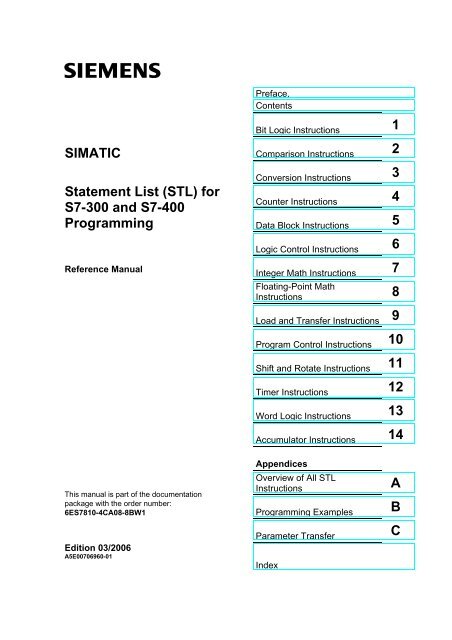
SIMATIC<br />
<strong>Statement</strong> <strong>List</strong> (<strong>STL</strong>) for<br />
S7-300 and S7-400<br />
Programming<br />
Reference Manual<br />
This manual is part of the documentation<br />
package with the order number:<br />
6ES7810-4CA08-8BW1<br />
Edition 03/2006<br />
A5E00706960-01<br />
Preface,<br />
Contents<br />
Bit Logic Instructions<br />
Comparison Instructions<br />
Conversion Instructions<br />
Counter Instructions<br />
Data Block Instructions<br />
Logic Control Instructions<br />
Integer Math Instructions<br />
Floating-Point Math<br />
Instructions<br />
1<br />
2<br />
3<br />
4<br />
5<br />
6<br />
7<br />
8<br />
Load and Transfer Instructions 9<br />
Program Control Instructions<br />
Shift and Rotate Instructions<br />
Timer Instructions<br />
Word Logic Instructions<br />
Accumulator Instructions<br />
Appendices<br />
Overview of All <strong>STL</strong><br />
Instructions<br />
Programming Examples<br />
Parameter Transfer<br />
Index<br />
10<br />
11<br />
12<br />
13<br />
14<br />
A<br />
B<br />
C
Safety Guidelines<br />
!<br />
!<br />
!<br />
Qualified Personnel<br />
Prescribed Usage<br />
!<br />
Trademarks<br />
This manual contains notices you have to observe in order to ensure your personal safety, as well as to<br />
prevent damage to property. The notices referring to your personal safety are highlighted in the manual<br />
by a safety alert symbol, notices referring to property damage only have no safety alert symbol. The<br />
notices shown below are graded according to the degree of danger.<br />
Danger<br />
indicates that death or severe personal injury will result if proper precautions are not taken.<br />
Warning<br />
indicates that death or severe personal injury may result if proper precautions are not taken.<br />
Caution<br />
with a safety alert symbol indicates that minor personal injury can result if proper precautions are not<br />
taken.<br />
Caution<br />
without a safety alert symbol indicates that property damage can result if proper precautions are not<br />
taken.<br />
Notice<br />
indicates that an unintended result or situation can occur if the corresponding notice is not taken into<br />
account.<br />
If more than one degree of danger is present, the warning notice representing the highest degree of<br />
danger will be used. A notice warning of injury to persons with a safety alert symbol may also include a<br />
warning relating to property damage.<br />
The device/system may only be set up and used in conjunction with this documentation. Commissioning<br />
and operation of a device/system may only be performed by qualified personnel. Within the context of<br />
the safety notices in this documentation qualified persons are defined as persons who are authorized to<br />
commission, ground and label devices, systems and circuits in accordance with established safety<br />
practices and standards.<br />
Note the following:<br />
Warning<br />
This device and its components may only be used for the applications described in the catalog or the<br />
technical description, and only in connection with devices or components from other manufacturers<br />
which have been approved or recommended by Siemens.<br />
Correct, reliable operation of the product requires proper transport, storage, positioning and assembly<br />
as well as careful operation and maintenance.<br />
All names identified by ® are registered trademarks of the Siemens AG.<br />
The remaining trademarks in this publication may be trademarks whose use by third parties for their<br />
own purposes could violate the rights of the owner.<br />
Disclaimer of Liability<br />
We have reviewed the contents of this publication to ensure consistency with the hardware and<br />
software described. Since variance cannot be precluded entirely, we cannot guarantee full consistency.<br />
However, the information in this publication is reviewed regularly and any necessary corrections are<br />
included in subsequent editions.<br />
Siemens AG<br />
Automation and Drives<br />
Postfach 4848<br />
90437 NÜRNBERG<br />
GERMANY<br />
A5E00706960-01<br />
03/2006<br />
Copyright © Siemens AG 2006<br />
Technical data subject to change
Preface<br />
Purpose<br />
This manual is your guide to creating user programs in the <strong>Statement</strong> <strong>List</strong><br />
programming language <strong>STL</strong>.<br />
The manual also includes a reference section that describes the syntax and<br />
functions of the language elements of <strong>STL</strong>.<br />
Basic Knowledge Required<br />
The manual is intended for S7 programmers, operators, and maintenance/service<br />
personnel.<br />
In order to understand this manual, general knowledge of automation technology is<br />
required.<br />
In addition to, computer literacy and the knowledge of other working equipment<br />
similar to the PC (e.g. programming devices) under the operating systems<br />
MS Windows 2000 Professional, XP Professional or MS Windows Server 2003 are<br />
required.<br />
Scope of the Manual<br />
This manual is valid for release 5.4 of the STEP 7 programming software package.<br />
Compliance with Standards<br />
<strong>STL</strong> corresponds to the "Instruction <strong>List</strong>" language defined in the International<br />
Electrotechnical Commission's standard IEC 1131-3, although there are substantial<br />
differences with regard to the operations. For further details, refer to the table of<br />
standards in the STEP 7 file NORM_TBL.WRI.<br />
<strong>Statement</strong> <strong>List</strong> (<strong>STL</strong>) for S7-300 and S7-400 Programming<br />
A5E00706960-01 iii
Preface<br />
Requirements<br />
To use the <strong>Statement</strong> <strong>List</strong> manual effectively, you should already be familiar with<br />
the theory behind S7 programs which is documented in the online help for STEP 7.<br />
The language packages also use the STEP 7 standard software, so you should be<br />
familiar with handling this software and have read the accompanying<br />
documentation.<br />
This manual is part of the documentation package "STEP 7 Reference".<br />
The following table displays an overview of the STEP 7 documentation:<br />
Documentation Purpose Order Number<br />
STEP 7 Basic Information with<br />
Basic information for technical 6ES7810-4CA08-8BW0<br />
•<br />
•<br />
•<br />
Working with STEP 7,<br />
Getting Started Manual<br />
Programming with STEP 7<br />
Configuring Hardware and<br />
Communication Connections,<br />
STEP 7<br />
personnel describing the methods<br />
of implementing control tasks with<br />
STEP 7 and the S7-300/400<br />
programmable controllers.<br />
• From S5 to S7, Converter Manual<br />
STEP 7 Reference with<br />
Provides reference information 6ES7810-4CA08-8BW1<br />
•<br />
•<br />
Ladder Logic (LAD)/Function Block and describes the programming<br />
Diagram (FBD)/<strong>Statement</strong> <strong>List</strong> (<strong>STL</strong>) for languages LAD, FBD, and <strong>STL</strong>,<br />
S7-300/400 manuals<br />
and standard and system<br />
functions extending the scope of<br />
Standard and System Functions<br />
the STEP 7 basic information.<br />
for S7-300/400<br />
Volume 1 and Volume 2<br />
Online Helps Purpose Order Number<br />
Help on STEP 7 Basic information on<br />
programming and configuring<br />
hardware with STEP 7 in the form<br />
of an online help.<br />
Reference helps on <strong>STL</strong>/LAD/FBD<br />
Reference help on SFBs/SFCs<br />
Reference help on Organization Blocks<br />
Context-sensitive reference<br />
information.<br />
Part of the STEP 7<br />
Standard software.<br />
Part of the STEP 7<br />
Standard software.<br />
<strong>Statement</strong> <strong>List</strong> (<strong>STL</strong>) for S7-300 and S7-400 Programming<br />
iv A5E00706960-01
Preface<br />
Online Help<br />
The manual is complemented by an online help which is integrated in the software.<br />
This online help is intended to provide you with detailed support when using the<br />
software.<br />
The help system is integrated in the software via a number of interfaces:<br />
• The context-sensitive help offers information on the current context, for<br />
example, an open dialog box or an active window. You can open the contextsensitive<br />
help via the menu command Help > Context-Sensitive Help, by<br />
pressing F1 or by using the question mark symbol in the toolbar.<br />
Further Support<br />
• You can call the general Help on STEP 7 using the menu command Help ><br />
Contents or the "Help on STEP 7" button in the context-sensitive help window.<br />
• You can call the glossary for all STEP 7 applications via the "Glossary" button.<br />
This manual is an extract from the "Help on <strong>Statement</strong> <strong>List</strong>". As the manual and the<br />
online help share an identical structure, it is easy to switch between the manual<br />
and the online help.<br />
If you have any technical questions, please get in touch with your Siemens<br />
representative or responsible agent.<br />
You will find your contact person at:<br />
http://www.siemens.com/automation/partner<br />
You will find a guide to the technical documentation offered for the individual<br />
SIMATIC Products and Systems here at:<br />
http://www.siemens.com/simatic-tech-doku-portal<br />
The online catalog and order system is found under:<br />
http://mall.automation.siemens.com/<br />
Training Centers<br />
Siemens offers a number of training courses to familiarize you with the SIMATIC<br />
S7 automation system. Please contact your regional training center or our central<br />
training center in D 90327 Nuremberg, Germany for details:<br />
Telephone: +49 (911) 895-3200.<br />
Internet: http://www.sitrain.com<br />
<strong>Statement</strong> <strong>List</strong> (<strong>STL</strong>) for S7-300 and S7-400 Programming<br />
A5E00706960-01 v
Preface<br />
Technical Support<br />
You can reach the Technical Support for all A&D products<br />
• Via the Web formula for the Support Request<br />
http://www.siemens.com/automation/support-request<br />
• Phone: + 49 180 5050 222<br />
• Fax: + 49 180 5050 223<br />
Additional information about our Technical Support can be found on the Internet<br />
pages http://www.siemens.com/automation/service<br />
Service & Support on the Internet<br />
In addition to our documentation, we offer our Know-how online on the internet at:<br />
http://www.siemens.com/automation/service&support<br />
where you will find the following:<br />
• The newsletter, which constantly provides you with up-to-date information on<br />
your products.<br />
• The right documents via our Search function in Service & Support.<br />
• A forum, where users and experts from all over the world exchange their<br />
experiences.<br />
• Your local representative for Automation & Drives.<br />
• Information on field service, repairs, spare parts and more under "Services".<br />
<strong>Statement</strong> <strong>List</strong> (<strong>STL</strong>) for S7-300 and S7-400 Programming<br />
vi A5E00706960-01
Contents<br />
1 Bit Logic Instructions 1-1<br />
1.1 Overview of Bit Logic Instructions .................................................................... 1-1<br />
1.2 A And ............................................................................................................. 1-3<br />
1.3 AN And Not.................................................................................................... 1-4<br />
1.4 O Or ............................................................................................................... 1-5<br />
1.5 ON Or Not...................................................................................................... 1-6<br />
1.6 X Exclusive Or ............................................................................................... 1-7<br />
1.7 XN Exclusive Or Not...................................................................................... 1-8<br />
1.8 O And before Or ............................................................................................ 1-9<br />
1.9 A( And with Nesting Open ........................................................................... 1-10<br />
1.10 AN( And Not with Nesting Open .................................................................. 1-11<br />
1.11 O( Or with Nesting Open ............................................................................. 1-11<br />
1.12 ON( Or Not with Nesting Open .................................................................... 1-12<br />
1.13 X( Exclusive Or with Nesting Open ............................................................. 1-12<br />
1.14 XN( Exclusive Or Not with Nesting Open .................................................... 1-13<br />
1.15 ) Nesting Closed .......................................................................................... 1-14<br />
1.16 = Assign....................................................................................................... 1-16<br />
1.17 R Reset........................................................................................................ 1-17<br />
1.18 S Set ............................................................................................................ 1-18<br />
1.19 NOT Negate RLO ........................................................................................ 1-19<br />
1.20 SET Set RLO (=1) ....................................................................................... 1-20<br />
1.21 CLR Clear RLO (=0) .................................................................................... 1-21<br />
1.22 SAVE Save RLO in BR Register ................................................................. 1-22<br />
1.23 FN Edge Negative ....................................................................................... 1-23<br />
1.24 FP Edge Positive ......................................................................................... 1-25<br />
2 Comparison Instructions 2-1<br />
2.1 Overview of Comparison Instructions............................................................... 2-1<br />
2.2 ? I Compare Integer (16-Bit)............................................................................ 2-2<br />
2.3 ? D Compare Double Integer (32-Bit).............................................................. 2-3<br />
2.4 ? R Compare Floating-Point Number (32-Bit) ................................................. 2-4<br />
3 Conversion Instructions 3-1<br />
3.1 Overview of Conversion Instructions ................................................................ 3-1<br />
3.2 BTI BCD to Integer (16-Bit) ........................................................................... 3-2<br />
3.3 ITB Integer (16-Bit) to BCD ........................................................................... 3-3<br />
3.4 BTD BCD to Integer (32-Bit).......................................................................... 3-4<br />
3.5 ITD Integer (16 Bit) to Double Integer (32-Bit) .............................................. 3-5<br />
3.6 DTB Double Integer (32-Bit) to BCD ............................................................. 3-6<br />
3.7 DTR Double Integer (32-Bit) to Floating-Point (32-Bit IEEE-FP) ................... 3-7<br />
3.8 INVI Ones Complement Integer (16-Bit)........................................................ 3-8<br />
3.9 INVD Ones Complement Double Integer (32-Bit) ......................................... 3-9<br />
3.10 NEGI Twos Complement Integer (16-Bit).................................................... 3-10<br />
3.11 NEGD Twos Complement Double Integer (32-Bit)...................................... 3-11<br />
3.12 NEGR Negate Floating-Point Number (32-Bit, IEEE-FP)............................ 3-12<br />
3.13 CAW Change Byte Sequence in ACCU 1-L (16-Bit) ................................... 3-13<br />
3.14 CAD Change Byte Sequence in ACCU 1 (32-Bit) ....................................... 3-14<br />
3.15 RND Round ................................................................................................. 3-15<br />
<strong>Statement</strong> <strong>List</strong> (<strong>STL</strong>) for S7-300 and S7-400 Programming<br />
A5E00706960-01 vii
Contents<br />
3.16 TRUNC Truncate ......................................................................................... 3-16<br />
3.17 RND+ Round to Upper Double Integer........................................................ 3-17<br />
3.18 RND- Round to Lower Double Integer......................................................... 3-18<br />
4 Counter Instructions 4-1<br />
4.1 Overview of Counter Instructions ..................................................................... 4-1<br />
4.2 FR Enable Counter (Free) ............................................................................. 4-2<br />
4.3 L Load Current Counter Value into ACCU 1 ................................................. 4-3<br />
4.4 LC Load Current Counter Value into ACCU 1 as BCD ................................. 4-4<br />
4.5 R Reset Counter ............................................................................................ 4-5<br />
4.6 S Set Counter Preset Value .......................................................................... 4-6<br />
4.7 CU Counter Up .............................................................................................. 4-7<br />
4.8 CD Counter Down.......................................................................................... 4-8<br />
5 Data Block Instructions 5-1<br />
5.1 Overview of Data Block Instructions................................................................. 5-1<br />
5.2 OPN Open a Data Block................................................................................ 5-2<br />
5.3 CDB Exchange Shared DB and Instance DB................................................ 5-3<br />
5.4 L DBLG Load Length of Shared DB in ACCU 1 ............................................ 5-4<br />
5.5 L DBNO Load Number of Shared DB in ACCU 1.......................................... 5-4<br />
5.6 L DILG Load Length of Instance DB in ACCU 1 ........................................... 5-5<br />
5.7 L DINO Load Number of Instance DB in ACCU 1 ......................................... 5-5<br />
6 Logic Control Instructions 6-1<br />
6.1 Overview of Logic Control Instructions............................................................. 6-1<br />
6.2 JU Jump Unconditional.................................................................................. 6-3<br />
6.3 JL Jump to Labels.......................................................................................... 6-4<br />
6.4 JC Jump if RLO = 1 ....................................................................................... 6-5<br />
6.5 JCN Jump if RLO = 0..................................................................................... 6-6<br />
6.6 JCB Jump if RLO = 1 with BR ....................................................................... 6-7<br />
6.7 JNB Jump if RLO = 0 with BR ....................................................................... 6-8<br />
6.8 JBI Jump if BR = 1......................................................................................... 6-9<br />
6.9 JNBI Jump if BR = 0 .................................................................................... 6-10<br />
6.10 JO Jump if OV = 1 ....................................................................................... 6-11<br />
6.11 JOS Jump if OS = 1..................................................................................... 6-12<br />
6.12 JZ Jump if Zero............................................................................................ 6-13<br />
6.13 JN Jump if Not Zero..................................................................................... 6-14<br />
6.14 JP Jump if Plus ............................................................................................ 6-15<br />
6.15 JM Jump if Minus......................................................................................... 6-16<br />
6.16 JPZ Jump if Plus or Zero ............................................................................. 6-17<br />
6.17 JMZ Jump if Minus or Zero.......................................................................... 6-18<br />
6.18 JUO Jump if Unordered............................................................................... 6-19<br />
6.19 LOOP Loop.................................................................................................. 6-20<br />
7 Integer Math Instructions 7-1<br />
7.1 Overview of Integer Math Instructions .............................................................. 7-1<br />
7.2 Evaluating the Bits of the Status Word with Integer Math Instructions............. 7-2<br />
7.3 +I Add ACCU 1 and ACCU 2 as Integer (16-Bit)........................................... 7-3<br />
7.4 -I Subtract ACCU 1 from ACCU 2 as Integer (16-Bit) ................................... 7-4<br />
7.5 *I Multiply ACCU 1 and ACCU 2 as Integer (16-Bit)...................................... 7-5<br />
7.6 /I Divide ACCU 2 by ACCU 1 as Integer (16-Bit) .......................................... 7-6<br />
7.7 + Add Integer Constant (16, 32-Bit)............................................................... 7-8<br />
7.8 +D Add ACCU 1 and ACCU 2 as Double Integer (32-Bit)........................... 7-10<br />
7.9 -D Subtract ACCU 1 from ACCU 2 as Double Integer (32-Bit) ................... 7-11<br />
7.10 *D Multiply ACCU 1 and ACCU 2 as Double Integer (32-Bit)...................... 7-12<br />
7.11 /D Divide ACCU 2 by ACCU 1 as Double Integer (32-Bit) .......................... 7-13<br />
7.12 MOD Division Remainder Double Integer (32-Bit) ...................................... 7-15<br />
<strong>Statement</strong> <strong>List</strong> (<strong>STL</strong>) for S7-300 and S7-400 Programming<br />
viii A5E00706960-01
Contents<br />
8 Floating-Point Math Instructions 8-1<br />
8.1 Overview of Floating-Point Math Instructions................................................... 8-1<br />
8.2 Evaluating the Bits of the Status Word with Floating-Point Math Instructions.. 8-2<br />
8.3 Floating-Point Math Instructions: Basic ............................................................ 8-3<br />
8.3.1 +R Add ACCU 1 and ACCU 2 as a Floating-Point Number<br />
(32-Bit IEEE-FP) ...............................................................................................8-3<br />
8.3.2 -R Subtract ACCU 1 from ACCU 2 as a Floating-Point Number<br />
(32-Bit IEEE-FP) ...............................................................................................8-5<br />
8.3.3 *R Multiply ACCU 1 and ACCU 2 as Floating-Point Numbers<br />
(32-Bit IEEE-FP) ...............................................................................................8-7<br />
8.3.4 /R Divide ACCU 2 by ACCU 1 as a Floating-Point Number<br />
(32-Bit IEEE-FP) ...............................................................................................8-8<br />
8.3.5 ABS Absolute Value of a Floating-Point Number (32-Bit IEEE-FP) ..............8-9<br />
8.4 Floating-Point Math Instructions: Extended.................................................... 8-10<br />
8.4.1 SQR Generate the Square of a Floating-Point Number (32-Bit) .................8-10<br />
8.4.2 SQRT Generate the Square Root of a Floating-Point Number (32-Bit) ......8-11<br />
8.4.3 EXP Generate the Exponential Value of a Floating-Point Number (32-Bit) 8-12<br />
8.4.4 LN Generate the Natural Logarithm of a Floating-Point Number (32-Bit) ...8-13<br />
8.4.5 SIN Generate the Sine of Angles as Floating-Point Numbers (32-Bit)........8-14<br />
8.4.6 COS Generate the Cosine of Angles as Floating-Point Numbers (32-Bit)..8-15<br />
8.4.7 TAN Generate the Tangent of Angles as Floating-Point Numbers (32-Bit) 8-16<br />
8.4.8 ASIN Generate the Arc Sine of a Floating-Point Number (32-Bit) ..............8-17<br />
8.4.9 ACOS Generate the Arc Cosine of a Floating-Point Number (32-Bit).........8-18<br />
8.4.10 ATAN Generate the Arc Tangent of a Floating-Point Number (32-Bit) .......8-19<br />
9 Load and Transfer Instructions 9-1<br />
9.1 Overview of Load and Transfer Instructions..................................................... 9-1<br />
9.2 L Load............................................................................................................ 9-2<br />
9.3 L STW Load Status Word into ACCU 1......................................................... 9-4<br />
9.4 LAR1 Load Address Register 1 from ACCU 1 .............................................. 9-5<br />
9.5 LAR1 Load Address Register 1 with Double Integer (32-Bit Pointer).... 9-6<br />
9.6 LAR1 AR2 Load Address Register 1 from Address Register 2..................... 9-7<br />
9.7 LAR2 Load Address Register 2 from ACCU 1 .............................................. 9-7<br />
9.8 LAR2 Load Address Register 2 with Double Integer (32-Bit Pointer).... 9-8<br />
9.9 T Transfer ...................................................................................................... 9-9<br />
9.10 T STW Transfer ACCU 1 into Status Word ................................................. 9-10<br />
9.11 CAR Exchange Address Register 1 with Address Register 2 ..................... 9-11<br />
9.12 TAR1 Transfer Address Register 1 to ACCU 1 ........................................... 9-11<br />
9.13 TAR1 Transfer Address Register 1 to Destination (32-Bit Pointer)..... 9-12<br />
9.14 TAR1 AR2 Transfer Address Register 1 to Address Register 2 ................. 9-13<br />
9.15 TAR2 Transfer Address Register 2 to ACCU 1 ........................................... 9-13<br />
9.16 TAR2 Transfer Address Register 2 to Destination (32-Bit Pointer)..... 9-14<br />
10 Program Control Instructions 10-1<br />
10.1 Overview of Program Control Instructions...................................................... 10-1<br />
10.2 BE Block End............................................................................................... 10-2<br />
10.3 BEC Block End Conditional ......................................................................... 10-3<br />
10.4 BEU Block End Unconditional ..................................................................... 10-4<br />
10.5 CALL Block Call........................................................................................... 10-5<br />
10.6 Call FB ............................................................................................................ 10-7<br />
10.7 Call FC............................................................................................................ 10-9<br />
10.8 Call SFB........................................................................................................ 10-11<br />
10.9 Call SFC ....................................................................................................... 10-13<br />
<strong>Statement</strong> <strong>List</strong> (<strong>STL</strong>) for S7-300 and S7-400 Programming<br />
A5E00706960-01 ix
Contents<br />
10.10 Call Multiple Instance.................................................................................... 10-14<br />
10.11 Call Block from a Library............................................................................... 10-14<br />
10.12 CC Conditional Call ................................................................................... 10-15<br />
10.13 UC Unconditional Call................................................................................ 10-16<br />
10.14 MCR (Master Control Relay) ........................................................................ 10-17<br />
10.15 Important Notes on Using MCR Functions................................................... 10-19<br />
10.16 MCR( Save RLO in MCR Stack, Begin MCR ............................................ 10-20<br />
10.17 )MCR End MCR......................................................................................... 10-22<br />
10.18 MCRA Activate MCR Area ........................................................................ 10-23<br />
10.19 MCRD Deactivate MCR Area .................................................................... 10-24<br />
11 Shift and Rotate Instructions 11-1<br />
11.1 Shift Instructions ............................................................................................. 11-1<br />
11.1.1 Overview of Shift Instructions .........................................................................11-1<br />
11.1.2 SSI Shift Sign Integer (16-Bit) .....................................................................11-2<br />
11.1.3 SSD Shift Sign Double Integer (32-Bit) .......................................................11-4<br />
11.1.4 SLW Shift Left Word (16-Bit) .......................................................................11-6<br />
11.1.5 SRW Shift Right Word (16-Bit) ....................................................................11-8<br />
11.1.6 SLD Shift Left Double Word (32-Bit)..........................................................11-10<br />
11.1.7 SRD Shift Right Double Word (32-Bit).......................................................11-12<br />
11.2 Rotate Instructions........................................................................................ 11-14<br />
11.2.1 Overview of Rotate Instructions....................................................................11-14<br />
11.2.2 RLD Rotate Left Double Word (32-Bit)......................................................11-15<br />
11.2.3 RRD Rotate Right Double Word (32-Bit)...................................................11-17<br />
11.2.4 RLDA Rotate ACCU 1 Left via CC 1 (32-Bit) ............................................11-19<br />
11.2.5 RRDA Rotate ACCU 1 Right via CC 1 (32-Bit) .........................................11-20<br />
12 Timer Instructions 12-1<br />
12.1 Overview of Timer Instructions ....................................................................... 12-1<br />
12.2 Location of a Timer in Memory and Components of a Timer ......................... 12-2<br />
12.3 FR Enable Timer (Free)............................................................................... 12-5<br />
12.4 L Load Current Timer Value into ACCU 1 as Integer .................................. 12-7<br />
12.5 LC Load Current Timer Value into ACCU 1 as BCD ................................... 12-9<br />
12.6 R Reset Timer............................................................................................ 12-11<br />
12.7 SP Pulse Timer.......................................................................................... 12-12<br />
12.8 SE Extended Pulse Timer ......................................................................... 12-14<br />
12.9 SD On-Delay Timer ................................................................................... 12-16<br />
12.10 SS Retentive On-Delay Timer ................................................................... 12-18<br />
12.11 SF Off-Delay Timer.................................................................................... 12-20<br />
13 Word Logic Instructions 13-1<br />
13.1 Overview of Word Logic Instructions .............................................................. 13-1<br />
13.2 AW AND Word (16-Bit)................................................................................ 13-2<br />
13.3 OW OR Word (16-Bit).................................................................................. 13-4<br />
13.4 XOW Exclusive OR Word (16-Bit) ............................................................... 13-6<br />
13.5 AD AND Double Word (32-Bit) .................................................................... 13-8<br />
13.6 OD OR Double Word (32-Bit) .................................................................... 13-10<br />
13.7 XOD Exclusive OR Double Word (32-Bit) ................................................. 13-12<br />
<strong>Statement</strong> <strong>List</strong> (<strong>STL</strong>) for S7-300 and S7-400 Programming<br />
x A5E00706960-01
Contents<br />
14 Accumulator Instructions 14-1<br />
14.1 Overview of Accumulator and Address Register Instructions ........................ 14-1<br />
14.2 TAK Toggle ACCU 1 with ACCU 2.............................................................. 14-2<br />
14.3 POP CPU with Two ACCUs ........................................................................ 14-3<br />
14.4 POP CPU with Four ACCUs........................................................................ 14-4<br />
14.5 PUSH CPU with Two ACCUs...................................................................... 14-5<br />
14.6 PUSH CPU with Four ACCUs ..................................................................... 14-6<br />
14.7 ENT Enter ACCU Stack............................................................................... 14-7<br />
14.8 LEAVE Leave ACCU Stack ......................................................................... 14-7<br />
14.9 INC Increment ACCU 1-L-L......................................................................... 14-8<br />
14.10 DEC Decrement ACCU 1-L-L...................................................................... 14-9<br />
14.11 +AR1 Add ACCU 1 to Address Register 1 ................................................ 14-10<br />
14.12 +AR2 Add ACCU 1 to Address Register 2 ................................................ 14-11<br />
14.13 BLD Program Display Instruction (Null)..................................................... 14-12<br />
14.14 NOP 0 Null Instruction ............................................................................... 14-12<br />
14.15 NOP 1 Null Instruction ............................................................................... 14-13<br />
A Overview of All <strong>STL</strong> Instructions A-1<br />
A.1 <strong>STL</strong> Instructions Sorted According to German Mnemonics (SIMATIC) ...........A-1<br />
A.2 <strong>STL</strong> Instructions Sorted According to English Mnemonics (International) .......A-7<br />
B Programming Examples B-1<br />
B.1 Overview of Programming Examples ...............................................................B-1<br />
B.2 Example: Bit Logic Instructions ........................................................................B-2<br />
B.3 Example: Timer Instructions .............................................................................B-7<br />
B.4 Example: Counter and Comparison Instructions............................................B-10<br />
B.5 Example: Integer Math Instructions ................................................................B-12<br />
B.6 Example: Word Logic Instructions ..................................................................B-13<br />
C Parameter Transfer C-1<br />
Index Index-1<br />
<strong>Statement</strong> <strong>List</strong> (<strong>STL</strong>) for S7-300 and S7-400 Programming<br />
A5E00706960-01 xi
Contents<br />
<strong>Statement</strong> <strong>List</strong> (<strong>STL</strong>) for S7-300 and S7-400 Programming<br />
xii A5E00706960-01
1 Bit Logic Instructions<br />
1.1 Overview of Bit Logic Instructions<br />
Description<br />
Bit logic instructions work with two digits, 1 and 0. These two digits form the base of<br />
a number system called the binary system. The two digits 1 and 0 are called binary<br />
digits or bits. In the world of contacts and coils, a 1 indicates activated or energized,<br />
and a 0 indicates not activated or not energized.<br />
The bit logic instructions interpret signal states of 1 and 0 and combine them<br />
according to Boolean logic. These combinations produce a result of 1 or 0 that is<br />
called the ”result of logic operation” (RLO).<br />
Boolean bit logic applies to the following basic instructions:<br />
• A And<br />
• AN And Not<br />
• O Or<br />
• ON Or Not<br />
• X Exclusive Or<br />
• XN Exclusive Or Not<br />
• O And before Or<br />
You can use the following instructions to perform nesting expressions:<br />
• A( And with Nesting Open<br />
• AN( And Not with Nesting Open<br />
• O( Or with Nesting Open<br />
• ON( Or Not with Nesting Open<br />
• X( Exclusive Or with Nesting Open<br />
• XN( Exclusive Or Not with Nesting Open<br />
• ) Nesting Closed<br />
<strong>Statement</strong> <strong>List</strong> (<strong>STL</strong>) for S7-300 and S7-400 Programming<br />
A5E00706960-01 1-1
Bit Logic Instructions<br />
You can terminate a Boolean bit logic string by using one of the following<br />
instructions:<br />
• = Assign<br />
• R Reset<br />
• S Set<br />
You can use one of the following instructions to change the result of logic operation<br />
(RLO):<br />
• NOT Negate RLO<br />
• SET Set RLO (=1)<br />
• CLR Clear RLO (=0)<br />
• SAVE Save RLO in BR Register<br />
Other instructions react to a positive or negative edge transition:<br />
• FN Edge Negative<br />
• FP Edge Positive<br />
<strong>Statement</strong> <strong>List</strong> (<strong>STL</strong>) for S7-300 and S7-400 Programming<br />
1-2 A5E00706960-01
1.2 A And<br />
Format<br />
A <br />
Address Data type Memory area<br />
BOOL I, Q, M, L, D, T, C<br />
Bit Logic Instructions<br />
Description<br />
A checks whether the state of the addressed bit is "1", and ANDs the test result with<br />
the RLO.<br />
Status Word Bit Checks:<br />
The AND instruction can also be used to directly check the status word by use of the<br />
following addresses: ==0, 0, >0, =0,
Bit Logic Instructions<br />
1.3 AN And Not<br />
Format<br />
N <br />
Address Data type Memory area<br />
BOOL I, Q, M, L, D, T, C<br />
Description<br />
AN checks whether the state of the addressed bit is "0", and ANDs the test result<br />
with the RLO.<br />
The AND NOT instruction can also be used to directly check the status word by use<br />
of the following addresses: ==0, 0, >0, =0,
1.4 O Or<br />
Format<br />
O <br />
Address Data type Memory area<br />
BOOL I, Q, M, L, D, T, C<br />
Bit Logic Instructions<br />
Description<br />
O checks whether the state of the addressed bit is "1", and ORs the test result with<br />
the RLO.<br />
Status Word Bit Checks:<br />
The OR instruction can also be used to directly check the status word by use of the<br />
following addresses: ==0, 0, >0, =0,
Bit Logic Instructions<br />
1.5 ON Or Not<br />
Format<br />
ON <br />
Address Data type Memory area<br />
BOOL I, Q, M, L, D, T, C<br />
Description<br />
ON checks whether the state of the addressed bit is "0", and ORs the test result with<br />
the RLO.<br />
Status Word Bit Checks:<br />
The OR NOT instruction can also be used to directly check the status word by use of<br />
the following addresses: ==0, 0, >0, =0,
1.6 X Exclusive Or<br />
Format<br />
X <br />
Address Data type Memory area<br />
BOOL I, Q, M, L, D, T, C<br />
Bit Logic Instructions<br />
Description<br />
X checks whether the state of the addressed bit is "1", and XORs the test result with<br />
the RLO.<br />
You can also use the Exclusive OR function several times. The mutual result of<br />
logic operation is then "1" if an impair number of checked addresses is "1".<br />
Status Word Bit Checks:<br />
The EXCLUSIVE OR instruction can also be used to directly check the status word<br />
by use of the following addresses: ==0, 0, >0, =0,
Bit Logic Instructions<br />
1.7 XN Exclusive Or Not<br />
Format<br />
XN <br />
Address Data type Memory area<br />
BOOL I, Q, M, L, D, T, C<br />
Description<br />
XN checks whether the state of the addressed bit is "0", and XORs the test result<br />
with the RLO.<br />
Status Word Bit Checks:<br />
The EXCLUSIVE OR NOT instruction can also be used to directly check the status<br />
word by use of the following addresses: ==0, 0, >0, =0,
1.8 O And before Or<br />
Format<br />
Description<br />
O<br />
Status word<br />
Example<br />
Bit Logic Instructions<br />
The O function performs a logical OR instruction on AND functions according to the<br />
rule: AND before OR.<br />
BR CC 1 CC 0 OV OS OR STA RLO /FC<br />
writes: - - - - - x 1 - x<br />
<strong>Statement</strong> <strong>List</strong> Program<br />
A I 0.0<br />
A M 10.0<br />
O<br />
A I 0.2<br />
A M 0.3<br />
O M 10.1<br />
= Q 4.0<br />
Power rail<br />
Q 4.0<br />
Coil<br />
<strong>Statement</strong> <strong>List</strong> (<strong>STL</strong>) for S7-300 and S7-400 Programming<br />
A5E00706960-01 1-9<br />
I 0.0<br />
M 10.0<br />
Relay Logic<br />
I 0.2<br />
M 0.3<br />
M 10.1
Bit Logic Instructions<br />
1.9 A( And with Nesting Open<br />
Description<br />
Format<br />
A(<br />
Status word<br />
Example<br />
A( (AND nesting open) saves the RLO and OR bits and a function code into the<br />
nesting stack. A maximum of seven nesting stack entries are possible.<br />
BR CC 1 CC 0 OV OS OR STA RLO /FC<br />
writes: - - - - - 0 1 - 0<br />
<strong>Statement</strong> <strong>List</strong> Program<br />
A(<br />
O I 0.0<br />
O M 10.0<br />
)<br />
A(<br />
O I 0.2<br />
O M 10.3<br />
)<br />
= Q 4.0<br />
Power rail<br />
Q 4.0<br />
Coil<br />
<strong>Statement</strong> <strong>List</strong> (<strong>STL</strong>) for S7-300 and S7-400 Programming<br />
1-10 A5E00706960-01<br />
I 0.0<br />
I 0.2<br />
A M 10.1 M 10.1<br />
Relay Logic<br />
M 10.0<br />
M10.3
1.10 AN( And Not with Nesting Open<br />
Format<br />
Description<br />
Status word<br />
AN(<br />
Bit Logic Instructions<br />
AN( (AND NOT nesting open) saves the RLO and OR bits and a function code into<br />
the nesting stack. A maximum of seven nesting stack entries are possible.<br />
BR CC 1 CC 0 OV OS OR STA RLO /FC<br />
writes: - - - - - 0 1 - 0<br />
1.11 O( Or with Nesting Open<br />
Format<br />
O(<br />
Description<br />
O( (OR nesting open) saves the RLO and OR bits and a function code into the<br />
nesting stack. A maximum of seven nesting stack entries are possible.<br />
Status word<br />
BR CC 1 CC 0 OV OS OR STA RLO /FC<br />
writes: - - - - - 0 1 - 0<br />
<strong>Statement</strong> <strong>List</strong> (<strong>STL</strong>) for S7-300 and S7-400 Programming<br />
A5E00706960-01 1-11
Bit Logic Instructions<br />
1.12 ON( Or Not with Nesting Open<br />
Format<br />
Description<br />
Status word<br />
ON(<br />
ON( (OR NOT nesting open) saves the RLO and OR bits and a function code into the<br />
nesting stack. A maximum of seven nesting stack entries is possible.<br />
BR CC 1 CC 0 OV OS OR STA RLO /FC<br />
writes: - - - - - 0 1 - 0<br />
1.13 X( Exclusive Or with Nesting Open<br />
Format<br />
Description<br />
X(<br />
Status word<br />
X( (XOR nesting open) saves the RLO and OR bits and a function code into the<br />
nesting stack. A maximum of seven nesting stack entries is possible.<br />
BR CC 1 CC 0 OV OS OR STA RLO /FC<br />
writes: - - - - - 0 1 - 0<br />
<strong>Statement</strong> <strong>List</strong> (<strong>STL</strong>) for S7-300 and S7-400 Programming<br />
1-12 A5E00706960-01
1.14 XN( Exclusive Or Not with Nesting Open<br />
Format<br />
Description<br />
Status word<br />
XN(<br />
Bit Logic Instructions<br />
XN( (XOR NOT nesting open) saves the RLO and OR bits and a function code into<br />
the nesting stack. A maximum of seven nesting stack entries is possible.<br />
BR CC 1 CC 0 OV OS OR STA RLO /FC<br />
writes: - - - - - 0 1 - 0<br />
<strong>Statement</strong> <strong>List</strong> (<strong>STL</strong>) for S7-300 and S7-400 Programming<br />
A5E00706960-01 1-13
Bit Logic Instructions<br />
1.15 ) Nesting Closed<br />
Format<br />
)<br />
Description<br />
Status word<br />
) (nesting closed) removes an entry from the nesting stack, restores the OR bit,<br />
interconnects the RLO that is contained in the stack entry with the current RLO<br />
according to the function code, and assigns the result to the RLO. The OR bit is also<br />
included if the function code is "AND" or "AND NOT".<br />
<strong>Statement</strong>s which open parentheses groups:<br />
• U( And with Nesting Open<br />
• UN( And Not with Nesting Open<br />
• O( Or with Nesting Open<br />
• ON( Or Not with Nesting Open<br />
• X( Exclusive Or with Nesting Open<br />
• XN( Exclusive Or Not with Nesting Open<br />
BR CC 1 CC 0 OV OS OR STA RLO /FC<br />
writes: - - - - - x 1 x 1<br />
<strong>Statement</strong> <strong>List</strong> (<strong>STL</strong>) for S7-300 and S7-400 Programming<br />
1-14 A5E00706960-01
Example<br />
<strong>Statement</strong> <strong>List</strong> Program<br />
A(<br />
O I 0.0<br />
O M 10.0<br />
)<br />
A(<br />
O I 0.2<br />
O M 10.3<br />
)<br />
= Q 4.0<br />
Power rail<br />
Q 4.0<br />
Coil<br />
Relay Logic<br />
Bit Logic Instructions<br />
<strong>Statement</strong> <strong>List</strong> (<strong>STL</strong>) for S7-300 and S7-400 Programming<br />
A5E00706960-01 1-15<br />
I 0.0<br />
I 0.2<br />
A M 10.1 M 10.1<br />
M 10.0<br />
M10.3
Bit Logic Instructions<br />
1.16 = Assign<br />
Format<br />
<br />
Address Data type Memory area<br />
BOOL I, Q, M, L, D<br />
Description<br />
= writes the RLO into the addressed bit for a switched on master control relay<br />
if MCR = 1. If MCR = 0, then the value 0 is written to the addressed bit instead of<br />
RLO.<br />
Status word<br />
Example<br />
BR CC 1 CC 0 OV OS OR STA RLO /FC<br />
writes: - - - - - 0 x - 0<br />
I 1.0<br />
Q 4.0<br />
<strong>Statement</strong> <strong>List</strong> Program Relay Logic<br />
A I 1.0<br />
= Q 4.0<br />
Signal state diagrams<br />
<strong>Statement</strong> <strong>List</strong> (<strong>STL</strong>) for S7-300 and S7-400 Programming<br />
1-16 A5E00706960-01<br />
1<br />
0<br />
1<br />
0<br />
Power<br />
rail<br />
I 1.0<br />
Q 4.0<br />
Coil
1.17 R Reset<br />
Format<br />
R <br />
Address Data type Memory area<br />
BOOL I, Q, M, L, D<br />
Bit Logic Instructions<br />
Description<br />
R (reset bit) places a "0" in the addressed bit if RLO = 1 and master control relay<br />
MCR = 1. If MCR = 0, then the addressed bit will not be changed.<br />
Status word<br />
Example<br />
BR CC 1 CC 0 OV OS OR STA RLO /FC<br />
writes: - - - - - 0 x - 0<br />
<strong>STL</strong> Program<br />
A I 1.0<br />
S Q 4.0<br />
A I 1.1<br />
R Q 4.0<br />
Signal state diagrams<br />
I 1.0<br />
I 1.1<br />
Q 4.0<br />
1<br />
0<br />
1<br />
0<br />
1<br />
0<br />
Power rail<br />
I 1.0<br />
NO contact<br />
NC Contact<br />
Q 4.0<br />
Coils<br />
Relay Logic<br />
Q 4.0<br />
<strong>Statement</strong> <strong>List</strong> (<strong>STL</strong>) for S7-300 and S7-400 Programming<br />
A5E00706960-01 1-17<br />
I 1.1
Bit Logic Instructions<br />
1.18 S Set<br />
Format<br />
S <br />
Address Data type Memory area<br />
BOOL I, Q, M, L, D<br />
Description of instruction<br />
S (set bit) places a "1" in the addressed bit if RLO = 1 and the switched on master<br />
control relay MCR = 1. If MCR = 0, the addressed bit does not change.<br />
Status word<br />
Example<br />
BR CC 1 CC 0 OV OS OR STA RLO /FC<br />
writes: - - - - - 0 x - 0<br />
I 1.0<br />
I 1.1<br />
Q 4.0<br />
<strong>Statement</strong> <strong>List</strong> Program Relay Logic<br />
A I 1.0<br />
S Q 4.0<br />
A I 1.1<br />
R Q4.0<br />
Signal state diagrams<br />
Power<br />
rail<br />
I 1.0<br />
NO<br />
contact<br />
Q 4.0<br />
Coil<br />
Q 4.0<br />
<strong>Statement</strong> <strong>List</strong> (<strong>STL</strong>) for S7-300 and S7-400 Programming<br />
1-18 A5E00706960-01<br />
1<br />
0<br />
1<br />
0<br />
1<br />
0<br />
NC<br />
contact<br />
Coil<br />
I 1.1
1.19 NOT Negate RLO<br />
Format<br />
Description<br />
Status word<br />
NOT<br />
NOT negates the RLO.<br />
Bit Logic Instructions<br />
BR CC 1 CC 0 OV OS OR STA RLO /FC<br />
writes: - - - - - - 1 x -<br />
<strong>Statement</strong> <strong>List</strong> (<strong>STL</strong>) for S7-300 and S7-400 Programming<br />
A5E00706960-01 1-19
Bit Logic Instructions<br />
1.20 SET Set RLO (=1)<br />
Format<br />
Description<br />
Status word<br />
Example<br />
SET<br />
SET sets the RLO to signal state "1".<br />
BR CC 1 CC 0 OV OS OR STA RLO /FC<br />
writes: - - - - - 0 1 1 0<br />
<strong>STL</strong> Program Signal State Result of Logic Operation (RLO)<br />
SET<br />
1<br />
= M 10.0<br />
= M 15.1<br />
= M 16.0<br />
CLR<br />
= M 10.1<br />
= M 10.2<br />
1<br />
1<br />
1<br />
0<br />
0<br />
<strong>Statement</strong> <strong>List</strong> (<strong>STL</strong>) for S7-300 and S7-400 Programming<br />
1-20 A5E00706960-01<br />
0
1.21 CLR Clear RLO (=0)<br />
Format<br />
Description<br />
Status word<br />
Example<br />
CLR<br />
CLR sets the RLO to signal state "0".<br />
Bit Logic Instructions<br />
BR CC 1 CC 0 OV OS OR STA RLO /FC<br />
writes: - - - - - 0 0 0 0<br />
<strong>Statement</strong> <strong>List</strong> Signal State Result of Logic Operation (RLO)<br />
SET<br />
1<br />
= M 10.0<br />
1<br />
= M 15.1<br />
1<br />
= M 16.0<br />
1<br />
CLR<br />
0<br />
= M 10.1<br />
0<br />
= M 10.2<br />
0<br />
<strong>Statement</strong> <strong>List</strong> (<strong>STL</strong>) for S7-300 and S7-400 Programming<br />
A5E00706960-01 1-21
Bit Logic Instructions<br />
1.22 SAVE Save RLO in BR Register<br />
Format<br />
SAVE<br />
Description of instruction<br />
Status word<br />
SAVE saves the RLO into the BR bit. The first check bit /FC is not reset. For this<br />
reason, the status of the BR bit is included in the AND logic operation in the next<br />
network.<br />
The use of SAVE and a subsequent query of the BR bit in the same block or in<br />
secondary blocks is not recommended because the BR bit can be changed by<br />
numerous instructions between the two. It makes sense to use the SAVE instruction<br />
before exiting a block because this sets the ENO output (= BR bit) to the value of the<br />
RLO bit and you can then add error handling of the block to this.<br />
BR CC 1 CC 0 OV OS OR STA RLO /FC<br />
writes: x - - - - - - - -<br />
<strong>Statement</strong> <strong>List</strong> (<strong>STL</strong>) for S7-300 and S7-400 Programming<br />
1-22 A5E00706960-01
1.23 FN Edge Negative<br />
Format<br />
FN <br />
Bit Logic Instructions<br />
Address Data type Memory area Description<br />
BOOL I, Q, M, L, D Edge flag, stores the previous<br />
signal state of RLO.<br />
Description<br />
FN (Negative RLO edge) detects a falling edge when the RLO transitions from<br />
"1" to "0", and indicates this by RLO = 1.<br />
During each program scan cycle, the signal state of the RLO bit is compared with<br />
that obtained in the previous cycle to see if there has been a state change. The<br />
previous RLO state must be stored in the edge flag address () to make the<br />
comparison. If there is a difference between current and previous RLO "1" state<br />
(detection of falling edge), the RLO bit will be "1" after this instruction.<br />
Status word<br />
Definition<br />
Note<br />
The instruction has no point if the bit you want to monitor is in the process image<br />
because the local data for a block are only valid during the block's runtime.<br />
BR CC 1 CC 0 OV OS OR STA RLO /FC<br />
writes: - - - - - 0 x x 1<br />
RLO<br />
1<br />
0<br />
Positive Edge Negative Edge<br />
Time<br />
<strong>Statement</strong> <strong>List</strong> (<strong>STL</strong>) for S7-300 and S7-400 Programming<br />
A5E00706960-01 1-23
Bit Logic Instructions<br />
Example<br />
If the programmable logic controller detects a negative edge at contact I 1.0, it<br />
energizes the coil at Q 4.0 for one OB1 scan cycle.<br />
<strong>Statement</strong> <strong>List</strong><br />
A I 1.0<br />
FN M 1.0<br />
= Q 4.0<br />
I 1.0<br />
OB1 Scan Cycle No:<br />
M 1.0<br />
Q 4.0<br />
Signal State Diagram<br />
1 2 3 4 5 6 7 8 9<br />
<strong>Statement</strong> <strong>List</strong> (<strong>STL</strong>) for S7-300 and S7-400 Programming<br />
1-24 A5E00706960-01<br />
1<br />
0<br />
1<br />
0<br />
1<br />
0
1.24 FP Edge Positive<br />
Format<br />
FP <br />
Bit Logic Instructions<br />
Address Data type Memory area Description<br />
BOOL I, Q, M, L, D Edge flag, stores the previous<br />
signal state of RLO.<br />
Description<br />
FP (Positive RLO edge) detects a rising edge when the RLO transitions from<br />
"0" to "1" and indicates this by RLO = 1.<br />
During each program scan cycle, the signal state of the RLO bit is compared with<br />
that obtained in the previous cycle to see if there has been a state change. The<br />
previous RLO state must be stored in the edge flag address () to make the<br />
comparison. If there is a difference between current and previous RLO "0" state<br />
(detection of rising edge), the RLO bit will be "1" after this instruction.<br />
Status word<br />
Definition<br />
Note<br />
The instruction has no point if the bit you want to monitor is in the process image<br />
because the local data for a block are only valid during the block's runtime.<br />
BR CC 1 CC 0 OV OS OR STA RLO /FC<br />
writes: - - - - - 0 x x 1<br />
RLO<br />
1<br />
0<br />
Positive Edge Negative Edge<br />
Time<br />
<strong>Statement</strong> <strong>List</strong> (<strong>STL</strong>) for S7-300 and S7-400 Programming<br />
A5E00706960-01 1-25
Bit Logic Instructions<br />
Example<br />
If the programmable logic controller detects a positive edge at contact I 1.0, it<br />
energizes the coil at Q 4.0 for one OB1 scan cycle.<br />
<strong>Statement</strong> <strong>List</strong><br />
A I 1.0<br />
FP M 1.0<br />
= Q 4.0<br />
OB1 Scan Cycle No:<br />
I 1.0<br />
M 1.0<br />
Q 4.0<br />
Signal State Diagram<br />
1 2 3 4 5 6 7 8 9<br />
<strong>Statement</strong> <strong>List</strong> (<strong>STL</strong>) for S7-300 and S7-400 Programming<br />
1-26 A5E00706960-01<br />
1<br />
0<br />
1<br />
0<br />
1<br />
0
2 Comparison Instructions<br />
2.1 Overview of Comparison Instructions<br />
Description<br />
ACCU1 and ACCU2 are compared according to the type of comparison you choose:<br />
== ACCU1 is equal to ACCU2<br />
ACCU1 is not equal to ACCU2<br />
> ACCU1 is greater than ACCU2<br />
< ACCU1 is less than ACCU2<br />
>= ACCU1 is greater than or equal to ACCU2<br />
Comparison Instructions<br />
2.2 ? I Compare Integer (16-Bit)<br />
Format<br />
==I, I, >I, =I, ACCU 1 ACCU 2 = ACCU 1 ACCU 2 < ACCU 1<br />
==I 0 1 0<br />
I 1 0 1<br />
>I 1 0 0<br />
=I 1 1 0<br />
I //Compare if ACCU 2-L (MW10) is greater (>) than ACCU 1- L (IW24).<br />
= M 2.0 //RLO = 1 if MW10 > IW24.<br />
<strong>Statement</strong> <strong>List</strong> (<strong>STL</strong>) for S7-300 and S7-400 Programming<br />
2-2 A5E00706960-01
2.3 ? D Compare Double Integer (32-Bit)<br />
Format<br />
==D, D, >D, =D,
Comparison Instructions<br />
2.4 ? R Compare Floating-Point Number (32-Bit)<br />
Format<br />
==R, R, >R, =R,
3 Conversion Instructions<br />
3.1 Overview of Conversion Instructions<br />
Description<br />
You can use the following instructions to convert binary coded decimal numbers and<br />
integers to other types of numbers:<br />
• BTI BCD to Integer (16-Bit)<br />
• ITB Integer (16-Bit) to BCD<br />
• BTD BCD to Integer (32-Bit)<br />
• ITD Integer (16-Bit) to Double Integer (32-Bit)<br />
• DTB Double Integer (32-Bit) to BCD<br />
• DTR Double Integer (32-Bit) to Floating-Point (32-Bit IEEE-FP)<br />
You can use one of the following instructions to form the complement of an integer or<br />
to invert the sign of a floating-point number:<br />
• INVI Ones Complement Integer (16-Bit)<br />
• INVD Ones Complement Double Integer (32-Bit)<br />
• NEGI Twos Complement Integer (16-Bit)<br />
• NEGD Twos Complement Double Integer (32-Bit)<br />
• NEGR Negate Floating-Point Number (32-Bit, IEEE-FP)<br />
You can use the following Change Bit Sequence in Accumulator 1 instructions to<br />
reverse the order of bytes in the low word of accumulator 1 or in the entire<br />
accumulator:<br />
• CAW Change Byte Sequence in ACCU 1-L (16-Bit)<br />
• CAD Change Byte Sequence in ACCU 1 (32-Bit)<br />
You can use any of the following instructions to convert a 32-bit IEEE floating-point<br />
number in accumulator 1 to a 32-bit integer (double integer). The individual<br />
instructions differ in their method of rounding:<br />
• RND Round<br />
• TRUNC Truncate<br />
• RND+ Round to Upper Double Integer<br />
• RND- Round to Lower Double Integer<br />
<strong>Statement</strong> <strong>List</strong> (<strong>STL</strong>) for S7-300 and S7-400 Programming<br />
A5E00706960-01 3-1
Conversion Instructions<br />
3.2 BTI BCD to Integer (16-Bit)<br />
Format<br />
Description<br />
Status word<br />
Example<br />
BTI<br />
BTI (decimal to binary conversion of a 3-digit BCD number) interprets the contents of<br />
ACCU 1-L as a three-digit binary coded decimal number (BCD) and converts it to a<br />
16-bit integer. The result is stored in the low word of accumulator 1. The high word of<br />
accumulator 1 and accumulator 2 remain unchanged.<br />
BCD number in ACCU 1-L: The permissible value range for the BCD number is<br />
from "-999" to "+999". Bit 0 to bit 11 are interpreted as the value and bit 15 as the<br />
sign (0 = positive, 1= negative) of the BCD number. Bit 12 to bit 14 are not used in<br />
the conversion. If a decimal (4 bits) of the BCD number is in the invalid range of 10 to<br />
15, a BCDF error occurs during attempted conversion. In general, the CPU will go<br />
into STOP. However, you may design another error response by programming<br />
OB121 to handle this synchronous programming error.<br />
BR CC 1 CC 0 OV OS OR STA RLO /FC<br />
writes: - - - - - - - - -<br />
<strong>STL</strong> Explanation<br />
L MW10 //Load the BCD number into ACCU 1-L.<br />
BTI //Convert from BCD to integer; store result in ACCU 1-L.<br />
T MW20 //Transfer result (integer number) to MW20.<br />
BTI<br />
MW10<br />
MW20<br />
15... ...8 7... ...0<br />
0 0 0 0 1 0 0 1 0 0 0 1 0 1 0 1<br />
0<br />
" + " " 9 " " 1 " " 5 "<br />
0<br />
0<br />
0<br />
BCD to Integer<br />
0<br />
0<br />
1<br />
1<br />
1<br />
<strong>Statement</strong> <strong>List</strong> (<strong>STL</strong>) for S7-300 and S7-400 Programming<br />
3-2 A5E00706960-01<br />
0<br />
0<br />
1<br />
0<br />
0<br />
1<br />
1<br />
"+915" BCD<br />
"+915" Integer
3.3 ITB Integer (16-Bit) to BCD<br />
Format<br />
Description<br />
Status word<br />
Example<br />
ITB<br />
Conversion Instructions<br />
ITB (binary to decimal conversion of a 16-bit integer number) interprets the contents<br />
of ACCU 1-L as a 16-bit integer and converts it to a three-digit binary coded decimal<br />
number (BCD). The result is stored in the low word of accumulator 1. Bit 0 to bit 11<br />
contain the value of the BCD number. Bit 12 to bit 15 are set to the state of the sign<br />
(0000 = positive, 1111= negative) of the BCD number. The high word of accumulator<br />
1 and accumulator 2 remain unchanged.<br />
The BCD number can be in the range of "-999" to "+999." If the number is out of the<br />
permissible range, then the status bits OV and OS are set to 1.<br />
The instruction is executed without regard to, and without affecting, the RLO.<br />
BR CC 1 CC 0 OV OS OR STA RLO /FC<br />
writes: - - - x x - - - -<br />
<strong>STL</strong> Explanation<br />
L MW10 //Load the integer number into ACCU 1-L.<br />
ITB //Convert from integer to BCD (16-bit); store result in ACCU 1-L.<br />
T MW20 //Transfer result (BCD number) to MW20.<br />
ITB<br />
MW10<br />
MW20<br />
15... ...8 7... ...0<br />
1 1 1 1 1 1 1 0 0 1 1 0 0 0 1 1<br />
1<br />
1<br />
1<br />
1<br />
0<br />
1<br />
Integer to BCD<br />
0<br />
0<br />
" - " " 4 " " 1 " " 3 "<br />
0<br />
<strong>Statement</strong> <strong>List</strong> (<strong>STL</strong>) for S7-300 and S7-400 Programming<br />
A5E00706960-01 3-3<br />
0<br />
0<br />
1<br />
0<br />
0<br />
1<br />
1<br />
"-413" Integer<br />
"-413" BCD
Conversion Instructions<br />
3.4 BTD BCD to Integer (32-Bit)<br />
Format<br />
Description<br />
Status word<br />
Example<br />
BTD<br />
BTD (decimal to binary conversion of a 7-digit BCD number) interprets the contents<br />
of ACCU 1 as a seven digit binary coded decimal number (BCD) and converts it to a<br />
32-bit double integer. The result is stored in accumulator 1. Accumulator 2 remains<br />
unchanged.<br />
BCD number in ACCU 1: The permissible value range for the BCD number is from<br />
"-9,999,999" to "+9,999,999". Bit 0 to bit 27 are interpreted as the value and bit 31 as<br />
the sign (0 = positive, 1= negative) of the BCD number. Bit 28 to bit 30 are not used<br />
in the conversion.<br />
If any decimal digit (a 4-bit tetrad of the BCD coding) is in the invalid range of 10 to<br />
15, a BCDF error occurs during attempted conversion. In general, the CPU will go<br />
into STOP. However, you may design another error response by programming<br />
OB121 to handle this synchronous programming error.<br />
BR CC 1 CC 0 OV OS OR STA RLO /FC<br />
writes: - - - - - - - - -<br />
<strong>STL</strong> Explanation<br />
L MD10 //Load the BCD number into ACCU 1.<br />
BTD //Convert from BCD to integer; store result in ACCU 1.<br />
T MD20 //Transfer result (double integer number) to MD20.<br />
BTD<br />
MD10<br />
MD20<br />
" + " " 0 " " 1 " " 5 "<br />
31... ...16 15... ...0<br />
0 0 0 0 0 0 0 0 0 0 0 1 0 1 0 1 0 1 1 1 1 0 0 0 0 0 1 0 0 0 0 1<br />
BCD to Double Integer<br />
" 7 " " 8 " " 2 " " 1 "<br />
"+157821"<br />
0 0 0 0 0 0 0 0 0 0 0 0 0 0 1 0 0<br />
1 1 0 1 0 0 0 0 1 1 1 1 1 0 1<br />
"+157821"<br />
<strong>Statement</strong> <strong>List</strong> (<strong>STL</strong>) for S7-300 and S7-400 Programming<br />
3-4 A5E00706960-01
3.5 ITD Integer (16 Bit) to Double Integer (32-Bit)<br />
Format<br />
Description<br />
Status word<br />
Example<br />
ITD<br />
Conversion Instructions<br />
ITD (conversion of a 16-bit integer number to a 32-bit integer number) interprets the<br />
contents of ACCU 1-L as a 16-bit integer and converts it to a 32-bit double integer.<br />
The result is stored in accumulator 1. Accumulator 2 remains unchanged.<br />
BR CC 1 CC 0 OV OS OR STA RLO /FC<br />
writes: - - - - - - - - -<br />
<strong>STL</strong> Explanation<br />
L MW12 //Load the integer number into ACCU 1.<br />
ITD //Convert from integer (16-bit) to double integer (32-bit); store result in<br />
ACCU 1.<br />
T MD20 //Transfer result (double integer) to MD20.<br />
Example: MW12 = "-10" (Integer, 16-bit)<br />
Contents ACCU1-H ACCU1-L<br />
Bit 31 . . . . . . . . . . 16 15 . . . . . . . . . . 0<br />
before execution of ITD XXXX XXX XXX XXX 1111 1111 1111 0110<br />
X X X<br />
after execution of ITD 1111 1111 1111 1111 1111 1111 1111 0110<br />
(X = 0 or 1, bits are not used for conversion)<br />
<strong>Statement</strong> <strong>List</strong> (<strong>STL</strong>) for S7-300 and S7-400 Programming<br />
A5E00706960-01 3-5
Conversion Instructions<br />
3.6 DTB Double Integer (32-Bit) to BCD<br />
Format<br />
Description<br />
Status word<br />
Example<br />
DTB<br />
DTB (binary to decimal conversion of a 32-bit integer number) interprets the content<br />
of ACCU 1 as a 32-bit double integer and converts it to a seven-digit binary coded<br />
decimal number (BCD).The result is stored in accumulator 1. Bit 0 to bit 27 contain<br />
the value of the BCD number. Bit 28 to bit 31 are set to the state of the sign of the<br />
BCD number (0000 = positive, 1111 = negative). Accumulator 2 remains unchanged.<br />
The BCD number can be in the range of "-9,999,999" to "+9,999,999". If the number<br />
is out of the permissible range, then the status bits OV and OS are set to 1.<br />
BR CC 1 CC 0 OV OS OR STA RLO /FC<br />
writes: - - - x x - - - -<br />
<strong>STL</strong> Explanation<br />
L MD10 //Load the 32-bit integer into ACCU 1.<br />
DTB //Convert from integer (32-bit) to BCD, store result in ACCU 1.<br />
T MD20 //Transfer result (BCD number) to MD20.<br />
DTB<br />
MD10<br />
MD20<br />
31... ...16 15... ...0<br />
1 1 1 1 1 1 1 1 1 1 1 1 1 1 1 1 1 1 1 1 1 1 0 1 0 1 0 0 0 0 1 1<br />
Integer to BCD<br />
"-701" Integer<br />
1 1 1 1 0 0 0 0 0 0 0 0 0 0 0 0 0<br />
0 0 0 0 1 1 1 0 0 0 0 0 0 0 1<br />
" - " " 0 " " 0 " " 0 " " 0 " " 7 " " 0 " " 1 "<br />
"-701" BCD<br />
<strong>Statement</strong> <strong>List</strong> (<strong>STL</strong>) for S7-300 and S7-400 Programming<br />
3-6 A5E00706960-01
Conversion Instructions<br />
3.7 DTR Double Integer (32-Bit) to Floating-Point (32-Bit<br />
IEEE-FP)<br />
Format<br />
Description<br />
Status word<br />
Example<br />
DTR<br />
DTR (conversion of a 32-bit integer number to a 32-bit IEEE floating point number)<br />
interprets the content of ACCU 1 as a 32-bit double integer and converts it to a 32-bit<br />
IEEE floating point number. If necessary, the instruction rounds the result. (A 32-bit<br />
integer has a higher accuracy than a 32-bit floating point number). The result is<br />
stored in accumulator 1.<br />
BR CC 1 CC 0 OV OS OR STA RLO /FC<br />
writes: - - - - - - - - -<br />
<strong>STL</strong> Explanation<br />
L MD10 //Load the 32-bit integer into ACCU 1.<br />
DTR //Convert from double integer to floating point (32-bit IEEE FP); store result<br />
in ACCU 1.<br />
T MD20 //Transfer result (BCD number) to MD20.<br />
DTR<br />
MD10<br />
MD20<br />
0 0 0 0 0 0 0 0 0 0 0 0 0 0 0 0 0 0 0 0 0 0 0 1 1 1 1 1 0 1 0 0<br />
Integer (32 bit) to IEEE floating-point (32 Bit)<br />
"+500" Integer<br />
31 30... 22...<br />
...0<br />
0 1 0 0 0 0 1 1 1 1 1 1 1 0 1 0 0 0 0 0 0 0 0 0 0 0 0 0 0 0 0 0<br />
8-bit exponent<br />
1 bit<br />
Sign of the mantissa<br />
23-bit mantissa<br />
"+500" IEEE-FP<br />
<strong>Statement</strong> <strong>List</strong> (<strong>STL</strong>) for S7-300 and S7-400 Programming<br />
A5E00706960-01 3-7
Conversion Instructions<br />
3.8 INVI Ones Complement Integer (16-Bit)<br />
Format<br />
Description<br />
Status word<br />
Example<br />
INVI<br />
INVI (ones complement integer) forms the ones complement of the 16-bit value in<br />
ACCU 1-L. Forming the ones complement inverts the value bit by bit, that is, zeros<br />
replace ones and ones replace zeros. The result is stored in the low word of<br />
accumulator 1.<br />
BR CC 1 CC 0 OV OS OR STA RLO /FC<br />
writes: - - - - - - - - -<br />
<strong>STL</strong> Explanation<br />
L IW8 //Load value into ACCU 1-L.<br />
INVI //Form ones complement 16-bit.<br />
T MW10 //Transfer result to MW10.<br />
Contents ACCU1-L<br />
Bit 15 . . . . . . . . . . 0<br />
before execution of INVI 0110 0011 1010 1110<br />
after execution of INVI 1001 1100 0101 0001<br />
<strong>Statement</strong> <strong>List</strong> (<strong>STL</strong>) for S7-300 and S7-400 Programming<br />
3-8 A5E00706960-01
Conversion Instructions<br />
3.9 INVD Ones Complement Double Integer (32-Bit)<br />
Format<br />
Description<br />
Status word<br />
Example<br />
INVD<br />
INVD (ones complement double integer) forms the ones complement of the 32-bit<br />
value in ACCU 1. Forming the ones complement inverts the value bit by bit, that is,<br />
zeros replace ones, and ones replace zeros. The result is stored in accumulator 1.<br />
BR CC 1 CC 0 OV OS OR STA RLO /FC<br />
writes: - - - - - - - - -<br />
<strong>STL</strong> Explanation<br />
L ID8 //Load value into ACCU 1.<br />
INVD //Form ones complement (32-bit).<br />
T MD10 //Transfer result to MD10.<br />
Contents ACCU1-H ACCU1-L<br />
Bit 31 . .<br />
.<br />
. . . . . . .<br />
16<br />
15 . .<br />
.<br />
. . . . . . . 0<br />
before execution of INVD 0110 1111 1000 1100 0110 0011 1010 1110<br />
after execution of INVD 1001 0000 0111 0011 1001 1100 0101 0001<br />
<strong>Statement</strong> <strong>List</strong> (<strong>STL</strong>) for S7-300 and S7-400 Programming<br />
A5E00706960-01 3-9
Conversion Instructions<br />
3.10 NEGI Twos Complement Integer (16-Bit)<br />
Format<br />
Description<br />
Status word<br />
Example<br />
NEGI<br />
NEGI (twos complement integer) forms the twos complement of the 16-bit value in<br />
ACCU 1-L. Forming the twos complement inverts the value bit by bit, that is, zeros<br />
replace ones and ones replace zeros; then a "1" is added. The result is stored in the<br />
low word of accumulator 1. The twos complement instruction is equivalent to<br />
multiplication by "-1." The status bits CC 1, CC 0, OS, and OV are set as a function of<br />
the result of the operation.<br />
BR CC 1 CC 0 OV OS OR STA RLO /FC<br />
writes: - x x x x - - - -<br />
Status word generation CC 1 CC 0 OV OS<br />
Result = 0 0 0 0 -<br />
-32768 = 1 1 0 0 -<br />
Result = 2768 0 1 1 1<br />
<strong>STL</strong> Explanation<br />
L IW8 //Load value into ACCU 1-L.<br />
NEGI //Form twos complement 16-bit.<br />
T MW10 //Transfer result to MW10.<br />
Contents ACCU1-L<br />
Bit 15 . . . . . . . . . . 0<br />
before execution of NEGI 0101 1101 0011 1000<br />
after execution of NEGI 1010 0010 1100 1000<br />
<strong>Statement</strong> <strong>List</strong> (<strong>STL</strong>) for S7-300 and S7-400 Programming<br />
3-10 A5E00706960-01
Conversion Instructions<br />
3.11 NEGD Twos Complement Double Integer (32-Bit)<br />
Format<br />
Description<br />
Status word<br />
Example<br />
NEGD<br />
NEGD (twos complement double integer) forms the twos complement of the 32-bit<br />
value in ACCU 1. Forming the twos complement inverts the value bit by bit, that is,<br />
zeros replace ones and ones replace zeros; then a "1" is added. The result is stored<br />
in accumulator 1. The twos complement instruction is equivalent to a multiplication<br />
by "-1" The instruction is executed without regard to, and without affecting, the RLO.<br />
The status bits CC 1, CC 0, OS, and OV are set as a function of the result of the<br />
operation.<br />
BR CC 1 CC 0 OV OS OR STA RLO /FC<br />
writes: - x x x x - - - -<br />
Status word generation CC 1 CC 0 OV OS<br />
Result = 0 0 0 0 -<br />
-2.147.483.648 = 1 1 0 0 -<br />
Result = 2 147 483 648 0 1 1 1<br />
<strong>STL</strong> Explanation<br />
L ID8 //Load value into ACCU 1.<br />
NEGD //Generate twos complement (32-bit).<br />
T MD10 //Transfer result to MD10.<br />
Contents ACCU1-H ACCU1-L<br />
Bit 31 . . . . . . . . . . 16 15 . . . . . . . . . . 0<br />
before execution of<br />
NEGD<br />
0101 1111 0110 0100 0101 1101 0011 1000<br />
after execution of NEGD 1010 0000 1001 1011 1010 0010 1100 1000<br />
<strong>Statement</strong> <strong>List</strong> (<strong>STL</strong>) for S7-300 and S7-400 Programming<br />
A5E00706960-01 3-11
Conversion Instructions<br />
3.12 NEGR Negate Floating-Point Number (32-Bit, IEEE-FP)<br />
Format<br />
NEGR<br />
Description of instruction<br />
Status word<br />
Example<br />
NEGR (negate 32-bit IEEE floating-point number) negates the floating-point number<br />
(32-bit, IEEE-FP) in ACCU 1. The instruction inverts the state of bit 31 in ACCU 1<br />
(sign of the mantissa). The result is stored in accumulator 1.<br />
BR CC 1 CC 0 OV OS OR STA RLO /FC<br />
writes: - - - - - - - - -<br />
<strong>STL</strong> Explanation<br />
L ID8 //Load value into ACCU 1 (example: ID 8 = 1.5E+02).<br />
NEGR //Negate floating-point number (32-bit, IEEE-FP); stores the result in ACCU<br />
1.<br />
T MD10 //Transfer result to MD10 (example: result = -1.5E+02).<br />
<strong>Statement</strong> <strong>List</strong> (<strong>STL</strong>) for S7-300 and S7-400 Programming<br />
3-12 A5E00706960-01
Conversion Instructions<br />
3.13 CAW Change Byte Sequence in ACCU 1-L (16-Bit)<br />
Format<br />
Description<br />
Status word<br />
Example<br />
CAW<br />
CAW reverses the sequence of bytes in ACCU 1-L. The result is stored in the low<br />
word of accumulator 1. The high word of accumulator 1 and accumulator 2 remain<br />
unchanged.<br />
BR CC 1 CC 0 OV OS OR STA RLO /FC<br />
writes: - - - - - - - - -<br />
<strong>STL</strong> Explanation<br />
L MW10 //Load the value of MW10 into ACCU 1.<br />
CAW //Reverse the sequence of bytes in ACCU 1-L.<br />
T MW20 //Transfer the result to MW20.<br />
Contents ACCU1-H-H ACCU1-H-L ACCU1-L-H ACCU1-L-L<br />
before execution of CAW value A value B value C value D<br />
after execution of CAW value A value B value D value C<br />
<strong>Statement</strong> <strong>List</strong> (<strong>STL</strong>) for S7-300 and S7-400 Programming<br />
A5E00706960-01 3-13
Conversion Instructions<br />
3.14 CAD Change Byte Sequence in ACCU 1 (32-Bit)<br />
Format<br />
Description<br />
Status word<br />
Example<br />
CAD<br />
CAD reverses the sequence of bytes in ACCU 1. The result is stored in accumulator<br />
1. Accumulator 2 remains unchanged.<br />
BR CC 1 CC 0 OV OS OR STA RLO /FC<br />
writes: - - - - - - - - -<br />
<strong>STL</strong> Explanation<br />
L MD10 //Load the value of MD10 into ACCU 1.<br />
CAD //Reverse the sequence of bytes in ACCU 1.<br />
T MD20 //Transfer the results to MD20.<br />
Contents ACCU1-H-H ACCU1-H-L ACCU1-L-H ACCU1-L-L<br />
before execution of CAD value A value B value C value D<br />
after execution of CAD value D value C value B value A<br />
<strong>Statement</strong> <strong>List</strong> (<strong>STL</strong>) for S7-300 and S7-400 Programming<br />
3-14 A5E00706960-01
3.15 RND Round<br />
Format<br />
Description<br />
Status word<br />
Example<br />
RND<br />
Conversion Instructions<br />
RND (conversion of a 32-bit IEEE floating-point number to 32-bit integer) interprets<br />
the contents of ACCU 1 as a 32-bit IEEE floating-point number (32-bit, IEEE-FP).<br />
The instruction converts the 32-bit IEEE floating-point number to a 32-bit integer<br />
(double integer) and rounds the result to the nearest whole number. If the fractional<br />
part of the converted number is midway between an even and an odd result, the<br />
instruction chooses the even result. If the number is out of the permissible range,<br />
then the status bits OV and OS are set to 1. The result is stored in accumulator 1.<br />
Conversion is not performed and an overflow indicated in the event of a fault<br />
(utilization of a NaN or a floating-point number that cannot be represented as a 32-bit<br />
integer number).<br />
BR CC 1 CC 0 OV OS OR STA RLO /FC<br />
writes: - - - x x - - - -<br />
<strong>STL</strong> Explanation<br />
L MD10 //Load the floating-point number into ACCU 1-L.<br />
RND //Convert the floating-point number (32-bit, IEEE-FP) into an integer (32-bit)<br />
and round off the result.<br />
T MD20 //Transfer result (double integer number) to MD20.<br />
Value before conversion Value after conversion<br />
MD10 = "100.5" => RND => MD20 = "+100"<br />
MD10 = "-100.5" => RND => MD20 = "-100"<br />
<strong>Statement</strong> <strong>List</strong> (<strong>STL</strong>) for S7-300 and S7-400 Programming<br />
A5E00706960-01 3-15
Conversion Instructions<br />
3.16 TRUNC Truncate<br />
Format<br />
Description<br />
Status word<br />
Example<br />
TRUNC<br />
TRUNC (conversion of a 32-bit IEEE floating-point number to 32-bit integer)<br />
interprets the contents of ACCU 1 as a 32-bit IEEE floating-point number. The<br />
instruction converts the 32-bit IEEE floating-point number to a 32-bit integer (double<br />
integer). The result is the whole number part of the floating-point number to be<br />
converted (IEEE rounding mode "round to zero"). If the number is out of the<br />
permissible range, then the status bits OV and OS are set to 1. The result is stored in<br />
accumulator 1.<br />
Conversion is not performed and an overflow indicated in the event of a fault<br />
(utilization of a NaN or a floating-point number that cannot be represented as a 32-bit<br />
integer number).<br />
BR CC 1 CC 0 OV OS OR STA RLO /FC<br />
writes: - - - x x - - - -<br />
<strong>STL</strong> Explanation<br />
L MD10 //Load the floating-point number into ACCU 1-L.<br />
TRUN //Convert the floating-point number (32-bit, IEEE-FP) to an integer (32-bit)<br />
C<br />
and round result. Store the result in ACCU 1.<br />
T MD20 //Transfer result (double integer number) to MD20.<br />
Value before conversion Value after conversion<br />
MD10 = "100.5" => TRUNC => MD20 = "+100"<br />
MD10 = "-100.5" => TRUNC => MD20 = "-100"<br />
<strong>Statement</strong> <strong>List</strong> (<strong>STL</strong>) for S7-300 and S7-400 Programming<br />
3-16 A5E00706960-01
3.17 RND+ Round to Upper Double Integer<br />
Format<br />
Description<br />
Status word<br />
Example<br />
RND+<br />
Conversion Instructions<br />
RND+ (conversion of a 32-bit IEEE floating-point number to 32-bit integer) interprets<br />
the contents of ACCU 1 as a 32-bit IEEE floating-point number. The instruction<br />
converts the 32-bit IEEE floating-point number to a 32-bit integer (double integer)<br />
and rounds the result to the smallest whole number greater than or equal to the<br />
floating-point number that is converted (IEEE rounding mode "round to +infinity"). If<br />
the number is out of the permissible range, then the status bits OV and OS are set to<br />
1.The result is stored in accumulator 1.<br />
Conversion is not performed and an overflow is indicated in the event of a fault<br />
(utilization of a NaN or a floating-point number that cannot be represented as a 32-bit<br />
integer number.)<br />
BR CC 1 CC 0 OV OS OR STA RLO /FC<br />
writes: - - - x x - - - -<br />
<strong>STL</strong> Explanation<br />
L MD10 //Load the floating-point number (32-bit, IEEE-FP) into ACCU 1-L.<br />
RND+ //Convert the floating-point number (32-bit, IEEE-FP) to an integer (32-bit)<br />
and round result. Store output in ACCU 1.<br />
T MD20 //Transfer result (double integer number) to MD20.<br />
Value before conversion Value after conversion<br />
MD10 = "100.5" => RND+ => MD20 = "+100"<br />
MD10 = "-100.5" => RND+ => MD20 = "-100"<br />
<strong>Statement</strong> <strong>List</strong> (<strong>STL</strong>) for S7-300 and S7-400 Programming<br />
A5E00706960-01 3-17
Conversion Instructions<br />
3.18 RND- Round to Lower Double Integer<br />
Format<br />
Description<br />
Status word<br />
Example<br />
RND-<br />
RND- (conversion of a 32-bit IEEE floating-point number to 32-bit integer) interprets<br />
the contents of ACCU 1 as 32-bit IEEE floating-point number. The instruction<br />
converts the 32-bit IEEE floating-point number to a 32-bit integer (double integer)<br />
and rounds the result to the largest whole number less than or equal to the<br />
floating-point number that is converted (IEEE rounding mode "round to -infinity"). If<br />
the number is out of the permissible range, then the status bits OV and OS are set to<br />
1. The result is stored in accumulator 1.<br />
Conversion is not performed and an overflow indicated in the event of a fault<br />
(utilization of a NaN or a floating-point number that cannot be represented as a 32-bit<br />
integer number.)<br />
BR CC 1 CC 0 OV OS OR STA RLO /FC<br />
writes: - - - x x - - - -<br />
<strong>STL</strong> Explanation<br />
L MD10 //Load the floating-point number into ACCU 1-L.<br />
RND- //Convert the floating-point number (32-bit, IEEE-FP) to an integer (32-bit)<br />
and round result. Store result in ACCU 1.<br />
T MD20 //Transfer result (double integer number) to MD20.<br />
Value before conversion Value after conversion<br />
MD10 = "100.5" => RND- => MD20 = "+100"<br />
MD10 = "-100.5" => RND- => MD20 = "-100"<br />
<strong>Statement</strong> <strong>List</strong> (<strong>STL</strong>) for S7-300 and S7-400 Programming<br />
3-18 A5E00706960-01
4 Counter Instructions<br />
4.1 Overview of Counter Instructions<br />
Description<br />
A counter is a function element of the STEP 7 programming language that acounts.<br />
Counters have an area reserved for them in the memory of your CPU. This memory<br />
area reserves one 16-bit word for each counter. The statement list instruction set<br />
supports 256 counters. To find out how many counters are available in your CPU,<br />
please refer to the CPU technical data.<br />
Counter instructions are the only functions with access to the memory area.<br />
You can vary the count value within this range by using the following Counter<br />
instructions:<br />
• FR Enable Counter (Free)<br />
• L Load Current Counter Value into ACCU 1<br />
• LC Load Current Counter Value into ACCU 1 as BCD<br />
• R Reset Counter<br />
• S Set Counter Preset Value<br />
• CU Counter Up<br />
• CD Counter Down<br />
<strong>Statement</strong> <strong>List</strong> (<strong>STL</strong>) for S7-300 and S7-400 Programming<br />
A5E00706960-01 4-1
Counter Instructions<br />
4.2 FR Enable Counter (Free)<br />
Format<br />
Description<br />
Status word<br />
Example<br />
FR <br />
Address Data type Memory area Description<br />
COUNTER C Counter, range<br />
depends on CPU.<br />
When RLO transitions from "0" to "1", FR clears the edge-detecting flag<br />
that is used for setting and selecting upwards or downwards count of the addressed<br />
counter. Enable counter is not required to set a counter or for normal counting This<br />
means that in spite of a constant RLO of 1 for the Set Counter Preset Value, Counter<br />
Up, or Counter Down, these instructions are not executed again after the enable.<br />
BR CC 1 CC 0 OV OS OR STA RLO /FC<br />
writes: - - - - - 0 - - 0<br />
<strong>STL</strong> Explanation<br />
A I 2.0 //Check signal state at input I 2.0.<br />
FR C3 //Enable counter C3 when RLO transitions from 0 to 1.<br />
<strong>Statement</strong> <strong>List</strong> (<strong>STL</strong>) for S7-300 and S7-400 Programming<br />
4-2 A5E00706960-01
4.3 L Load Current Counter Value into ACCU 1<br />
Format<br />
Description<br />
Status word<br />
Example<br />
L <br />
Counter Instructions<br />
Address Data type Memory area Description<br />
COUNTER C Counter, range<br />
depends on CPU.<br />
L loads the current count of the addressed counter as an integer into<br />
ACCU 1-L after the contents of ACCU 1 have been saved into ACCU 2.<br />
BR CC 1 CC 0 OV OS OR STA RLO /FC<br />
writes: - - - - - - - - -<br />
<strong>STL</strong> Explanation<br />
L C3 //Load ACCU 1-L with the count value of counter C3 in binary format.<br />
Counter word<br />
for counter C3<br />
in memory<br />
Contents of<br />
ACCU1-L after<br />
Load instruction<br />
L C3<br />
2 15<br />
2 15<br />
2 14<br />
2 14<br />
2 13<br />
2 13<br />
2 12<br />
2 12<br />
All "0"<br />
2 11<br />
2 11<br />
2 10<br />
2 10<br />
2 9<br />
2 9<br />
Count value (0 to 999) in binary coding<br />
L C3<br />
Count value (0 to 999) in binary coding<br />
codiert<br />
<strong>Statement</strong> <strong>List</strong> (<strong>STL</strong>) for S7-300 and S7-400 Programming<br />
A5E00706960-01 4-3<br />
2 8<br />
2 8<br />
2 7<br />
2 7<br />
2 6<br />
2 6<br />
2 5<br />
2 5<br />
2 4<br />
2 4<br />
2 3<br />
2 3<br />
2 2<br />
2 2<br />
2 1<br />
2 1<br />
2 0<br />
2 0
Counter Instructions<br />
4.4 LC Load Current Counter Value into ACCU 1 as BCD<br />
Format<br />
Description<br />
Status word<br />
Example<br />
LC <br />
Address Data type Memory area Description<br />
COUNTER C Counter, range<br />
depends on CPU.<br />
LC loads the count of the addressed counter as a BCD number into<br />
ACCU 1 after the old contents of ACCU 1 have been saved into ACCU 2.<br />
BR CC 1 CC 0 OV OS OR STA RLO /FC<br />
writes: - - - - - - - - -<br />
<strong>STL</strong> Explanation<br />
LC C3 //Load ACCU 1-L with the count value of counter C3 in binary coded decimal<br />
format.<br />
Counter word<br />
for counter C3<br />
in memory<br />
Contents of<br />
ACCU1-L after<br />
Load instruction<br />
LC C3<br />
2 15<br />
0<br />
2 15<br />
2 14<br />
0<br />
2 14<br />
2 13<br />
0<br />
2 13<br />
2 12<br />
0<br />
2 12<br />
2 11<br />
2 11<br />
2 10<br />
2 10<br />
2 9<br />
2 9<br />
Counter value (0 to 999) in binary coding<br />
codiert<br />
LC Z3<br />
Counter value in BCD<br />
<strong>Statement</strong> <strong>List</strong> (<strong>STL</strong>) for S7-300 and S7-400 Programming<br />
4-4 A5E00706960-01<br />
2 8<br />
2 8<br />
10 2 Hundreds<br />
2 7<br />
2 7<br />
2 6<br />
2 6<br />
2 5<br />
2 5<br />
2 4<br />
2 4<br />
2 3<br />
2 3<br />
2 2<br />
2 2<br />
2 1<br />
2 1<br />
10 1 Tens 10 0 Ones<br />
2 0<br />
2 0
4.5 R Reset Counter<br />
Format<br />
Description<br />
Status word<br />
Example<br />
R <br />
Counter Instructions<br />
Address Data type Memory area Description<br />
COUNTER C Counter to be preset,<br />
range depends on<br />
CPU.<br />
R loads the addressed counter with "0" if RLO=1.<br />
BR CC 1 CC 0 OV OS OR STA RLO /FC<br />
writes: - - - - - 0 - - 0<br />
<strong>STL</strong> Explanation<br />
A I 2.3 //Check signal state at input I 2.3.<br />
R C3 //Reset counter C3 to a value of 0 if RLO transitions from 0 to 1.<br />
<strong>Statement</strong> <strong>List</strong> (<strong>STL</strong>) for S7-300 and S7-400 Programming<br />
A5E00706960-01 4-5
Counter Instructions<br />
4.6 S Set Counter Preset Value<br />
Format<br />
Description<br />
Status word<br />
Example<br />
S <br />
Address Data type Memory area Description<br />
COUNTER C Counter to be preset,<br />
range depends on<br />
CPU.<br />
S loads the count from ACCU 1-L into the addressed counter when the<br />
RLO transitions from "0" to "1". The count in ACCU 1 must be a BCD number<br />
between "0" and "999".<br />
BR CC 1 CC 0 OV OS OR STA RLO /FC<br />
writes: - - - - - 0 - - 0<br />
<strong>STL</strong> Explanation<br />
A I 2.3 //Check signal state at input I 2.3.<br />
L C#3 //Load count value 3 into ACCU 1-L.<br />
S C1 //Set counter C1 to count value if RLO transitions from 0 to 1.<br />
<strong>Statement</strong> <strong>List</strong> (<strong>STL</strong>) for S7-300 and S7-400 Programming<br />
4-6 A5E00706960-01
4.7 CU Counter Up<br />
Format<br />
CU <br />
Counter Instructions<br />
Address Data type Memory area Description<br />
COUNTER C Counter, range<br />
depends on CPU.<br />
Description<br />
CU increments the count of the addressed counter by 1 when RLO<br />
transitions from "0" to "1" and the count is less than "999". When the count reaches<br />
its upper limit of "999", incrementing stops. Additional transitions of RLO have no<br />
effect and overflow OV bit is not set.<br />
Status word<br />
Example<br />
BR CC 1 CC 0 OV OS OR STA RLO /FC<br />
writes: - - - - - 0 - - 0<br />
<strong>STL</strong> Explanation<br />
A I 2.1 //If there is a positive edge change at input I 2.1.<br />
CU C3 //Counter C3 is incremented by 1 when RL0 transitions from 0 to 1.<br />
<strong>Statement</strong> <strong>List</strong> (<strong>STL</strong>) for S7-300 and S7-400 Programming<br />
A5E00706960-01 4-7
Counter Instructions<br />
4.8 CD Counter Down<br />
Format<br />
CD <br />
Address Data type Memory area Description<br />
COUNTER C Counter, range<br />
depends on CPU.<br />
Description<br />
CD decrements the count of the addressed counter by 1 when RLO<br />
transitions from "0" to "1" and the count is greater than 0. When the count reaches its<br />
lower limit of "0", decrementing stops. Additional transitions of RLO have no effect as<br />
the counter will not count with negative values.<br />
Status word<br />
Example<br />
BR CC 1 CC 0 OV OS OR STA RLO /FC<br />
writes: - - - - - 0 - - 0<br />
<strong>STL</strong> Explanation<br />
L C#14 //Counter preset value.<br />
A I 0.1 //Preset counter after detection of rising edge of I 0.1.<br />
S C1 //Load counter 1 preset if enabled.<br />
A I 0.0 //One count down per rising edge of I 0.0.<br />
CD C1 //Decrement counter C1 by 1 when RL0 transitions from 0 to 1 depending on input<br />
I 0.0.<br />
AN C1 //Zero detection using the C1 bit.<br />
= Q 0.0 //Q 0.0 = 1 if counter 1 value is zero.<br />
<strong>Statement</strong> <strong>List</strong> (<strong>STL</strong>) for S7-300 and S7-400 Programming<br />
4-8 A5E00706960-01
5 Data Block Instructions<br />
5.1 Overview of Data Block Instructions<br />
Description<br />
You can use the Open a Data Block (OPN) instruction to open a data block as a<br />
shared data block or as an instance data block. The program itself can accomodate<br />
one open shared data block and one open instance data block at the same time.<br />
The following Data Block instructions are available:<br />
• OPN Open a Data Block<br />
• CDB Exchange Shared DB and Instance DB<br />
• L DBLG Load Length of Shared DB in ACCU 1<br />
• L DBNO Load Number of Shared DB in ACCU 1<br />
• L DILG Load Length of Instance DB in ACCU 1<br />
• L DINO Load Number of Instance DB in ACCU 1<br />
<strong>Statement</strong> <strong>List</strong> (<strong>STL</strong>) for S7-300 and S7-400 Programming<br />
A5E00706960-01 5-1
Data Block Instructions<br />
5.2 OPN Open a Data Block<br />
Format<br />
OPN <br />
Address Data block type Source address<br />
DB, DI 1 to 65535<br />
Description of instruction<br />
Status word<br />
Example<br />
OPN opens a data block as a shared data block or as an instance data<br />
block. One shared data block and one instance data block can be open at the same<br />
time.<br />
BR CC 1 CC 0 OV OS OR STA RLO /FC<br />
writes: - - - - - - - - -<br />
<strong>STL</strong> Explanation<br />
OPN DB10 //Open data block DB10 as a shared data block.<br />
L DBW35 //Load data word 35 of the opened data block into ACCU 1-L.<br />
T MW22 //Transfer the content of ACCU 1-L into MW22.<br />
OPN DI20 //Open data block DB20 as an instance data block.<br />
L DIB12 //Load data byte 12 of the opened instance data block into ACCU 1-L.<br />
T DBB37 //Transfer the content of ACCU 1-L to data byte 37 of the opened shared data<br />
block.<br />
<strong>Statement</strong> <strong>List</strong> (<strong>STL</strong>) for S7-300 and S7-400 Programming<br />
5-2 A5E00706960-01
5.3 CDB Exchange Shared DB and Instance DB<br />
Format<br />
CDB<br />
Description of instruction<br />
Status word<br />
Data Block Instructions<br />
CDB is used to exchange the shared data block and instance data block. The<br />
instruction swaps the data block registers. A shared data block becomes an instance<br />
data block and vice-versa.<br />
BR CC 1 CC 0 OV OS OR STA RLO /FC<br />
writes: - - - - - - - - -<br />
<strong>Statement</strong> <strong>List</strong> (<strong>STL</strong>) for S7-300 and S7-400 Programming<br />
A5E00706960-01 5-3
Data Block Instructions<br />
5.4 L DBLG Load Length of Shared DB in ACCU 1<br />
Format<br />
L DBLG<br />
Description of instruction<br />
Status word<br />
Example<br />
L DBLG (load length of shared data block) loads the length of the shared data block<br />
into ACCU 1 after the contents of ACCU 1 have been saved into ACCU 2.<br />
BR CC 1 CC 0 OV OS OR STA RLO /FC<br />
writes: - - - - - - - - -<br />
<strong>STL</strong> Explanation<br />
OPN DB10 //Open data block DB10 as shared data block.<br />
L DBLG //Load length of shared data block (length of DB10).<br />
L MD10 //Value for comparison if data block is long enough.<br />
Data Block Instructions<br />
5.6 L DILG Load Length of Instance DB in ACCU 1<br />
Format<br />
L DILG<br />
Description of instruction<br />
Status word<br />
Example<br />
L DILG (load length of instance data block) loads the length of the instance data<br />
block into ACCU 1-L after the content of ACCU 1 has been saved into ACCU 2.<br />
BR CC 1 CC 0 OV OS OR STA RLO /FC<br />
writes: - - - - - - - - -<br />
<strong>STL</strong> Explanation<br />
OPN D120 //Open data block DB20 as an instance data block.<br />
L DILG //Load length of instance data block (length of DB20).<br />
L MW10 //Value for comparison if data block is long enough.<br />
Data Block Instructions<br />
<strong>Statement</strong> <strong>List</strong> (<strong>STL</strong>) for S7-300 and S7-400 Programming<br />
5-6 A5E00706960-01
6 Logic Control Instructions<br />
6.1 Overview of Logic Control Instructions<br />
Description<br />
You can use the Jump instructions to control the flow of logic, enabling your program<br />
to interrupt its linear flow to resume scanning at a different point. You can use the<br />
LOOP instruction to call a program segment multiple times.<br />
The address of a Jump or Loop instruction is a label. A jump label may be as many<br />
as four characters, and the first character must be a letter. Jumps labels are followed<br />
with a mandatory colon ":" and must precede the program statement in a line.<br />
Note<br />
Please note for S7– 300 CPU programs that the jump destination always (not for<br />
318– 2) forms the beginning of a Boolean logic string in the case of jump<br />
instructions. The jump destination must not be included in the logic string.<br />
You can use the following jump instructions to interrupt the normal flow of your<br />
program unconditionally:<br />
• JU Jump Unconditional<br />
• JL Jump to Labels<br />
The following jump instructions interrupt the flow of logic in your program based on<br />
the result of logic operation (RLO) produced by the previous instruction statement:<br />
• JC Jump if RLO = 1<br />
• JCN Jump if RLO = 0<br />
• JCB Jump if RLO = 1 with BR<br />
• JNB Jump if RLO = 0 with BR<br />
The following jump instructions interrupt the flow of logic in your program based on<br />
the signal state of a bit in the status word:<br />
• JBI Jump if BR = 1<br />
• JNBI Jump if BR = 0<br />
• JO Jump if OV = 1<br />
• JOS Jump if OS = 1<br />
<strong>Statement</strong> <strong>List</strong> (<strong>STL</strong>) for S7-300 and S7-400 Programming<br />
A5E00706960-01 6-1
Logic Control Instructions<br />
The following jump instructions interrupt the flow of logic in your program based on<br />
the result of a calculation:<br />
• JZ Jump if Zero<br />
• JN Jump if Not Zero<br />
• JP Jump if Plus<br />
• JM Jump if Minus<br />
• JPZ Jump if Plus or Zero<br />
• JMZ Jump if Minus or Zero<br />
• JUO Jump if Unordered<br />
<strong>Statement</strong> <strong>List</strong> (<strong>STL</strong>) for S7-300 and S7-400 Programming<br />
6-2 A5E00706960-01
6.2 JU Jump Unconditional<br />
Format<br />
Description<br />
Status word<br />
Example<br />
JU <br />
Address Description<br />
Symbolic name of jump destination.<br />
Logic Control Instructions<br />
JU interrupts the linear program scan and jumps to a jump<br />
destination, regardless of the status word contents. The linear program scan<br />
resumes at the jump destination. The jump destination is specified by a jump label.<br />
Both forward and backward jumps are possible. Jumps may be executed only within<br />
a block, that is, the jump instruction and the jump destination must lie within one and<br />
the same block. The jump destination must be unique within this block. The<br />
maximum jump distance is -32768 or +32767 words of program code. The actual<br />
maximum number of statements you can jump over depends on the mix of the<br />
statements used in your program (one-, two-, or three word statements).<br />
BR CC 1 CC 0 OV OS OR STA RLO /FC<br />
writes: - - - - - - - - -<br />
<strong>STL</strong> Explanation<br />
A I 1.0<br />
A I 1.2<br />
JC DELE //Jump if RLO=1 to jump label DELE.<br />
L MB10<br />
INC 1<br />
T MB10<br />
JU FORW //Jump unconditionally to jump label FORW.<br />
DELE: L 0<br />
T MB10<br />
FORW: A I 2.1 //Program scan resumes here after jump to jump label FORW.<br />
<strong>Statement</strong> <strong>List</strong> (<strong>STL</strong>) for S7-300 and S7-400 Programming<br />
A5E00706960-01 6-3
Logic Control Instructions<br />
6.3 JL Jump to Labels<br />
Format<br />
Description<br />
Status word<br />
Example<br />
JL <br />
Address Description<br />
Symbolic name of jump destination.<br />
JL (jump via jump to list) enables multiple jumps to be programmed.<br />
The jump target list, with a maximum of 255 entries, begins on the next line after the<br />
JL instruction and ends on the line before the jump label referenced in the JL<br />
address. Each jump destination consists of one JU instruction. The number of jump<br />
destinations (0 to 255) is taken from ACCU 1-L-L.<br />
The JL instruction jumps to one of the JU instructions as long as the contents of the<br />
ACCU is smaller than the number of jump destinations between the JL instruction<br />
and the jump label. The first JU instruction is jumped to if ACCU 1-L-L=0. The<br />
second JU instruction is jumped to if ACCU 1-L-L=1, etc. The JL instruction jumps to<br />
the first instruction after the last JU instruction in the destination list if the number of<br />
jump destinations is too large.<br />
The jump destination list must consist of JU instructions which precede the jump<br />
label referenced in the address of the JL instruction. Any other instruction within the<br />
jump list is illegal.<br />
BR CC 1 CC 0 OV OS OR STA RLO /FC<br />
writes: - - - - - - - - -<br />
<strong>STL</strong> Explanation<br />
L MB0 //Load jump destination number into ACCU 1-L-L.<br />
JL LSTX //Jump destination if ACCU 1-L-L > 3.<br />
JU SEG0 //Jump destination if ACCU 1-L-L = 0.<br />
JU SEG1 //Jump destination if ACCU 1-L-L = 1.<br />
JU COMM //Jump destination if ACCU 1-L-L = 2.<br />
JU SEG3 //Jump destination if ACCU 1-L-L = 3.<br />
LSTX: JU COMM<br />
SEG0: * //Permitted instruction<br />
*<br />
JU COMM<br />
SEG1: * //Permitted instruction<br />
*<br />
JU COMM<br />
SEG3: * //Permitted instruction.<br />
*<br />
JU COMM<br />
COMM: *<br />
*<br />
<strong>Statement</strong> <strong>List</strong> (<strong>STL</strong>) for S7-300 and S7-400 Programming<br />
6-4 A5E00706960-01
6.4 JC Jump if RLO = 1<br />
Format<br />
Description<br />
Status word<br />
Example<br />
JC <br />
Address Description<br />
Symbolic name of jump destination.<br />
Logic Control Instructions<br />
If the result of logic operation is 1, JC interrupts the linear program<br />
scan and jumps to a jump destination. The linear program scan resumes at the jump<br />
destination. The jump destination is specified a jump label. Both forward and<br />
backward jumps are possible. Jumps may be executed only within a block, that is,<br />
the jump instruction and the jump destination must lie within one and the same block.<br />
The jump destination must be unique within this block. The maximum jump distance<br />
is -32768 or +32767 words of program code. The actual maximum number of<br />
statements you can jump over depends on the mix of the statements used in your<br />
program (one-, two-, or three word statements).<br />
If the result of logic operation is 0, the jump is not executed. The RLO is set to 1, and<br />
the program scan continues with the next statement.<br />
BR CC 1 CC 0 OV OS OR STA RLO /FC<br />
writes: - - - - - 0 1 1 0<br />
<strong>STL</strong> Explanation<br />
A I 1.0<br />
A I 1.2<br />
JC JOVR //Jump if RLO=1 to jump label JOVR.<br />
L IW8 //Program scan continues here if jump is not executed.<br />
T MW22<br />
JOVR: A I 2.1 //Program scan resumes here after jump to jump label JOVR.<br />
<strong>Statement</strong> <strong>List</strong> (<strong>STL</strong>) for S7-300 and S7-400 Programming<br />
A5E00706960-01 6-5
Logic Control Instructions<br />
6.5 JCN Jump if RLO = 0<br />
Format<br />
Description<br />
Status word<br />
Example<br />
JCN <br />
Address Description<br />
Symbolic name of jump destination.<br />
If the result of logic operation is 0, JCN interrupts the linear program<br />
scan and jumps to a jump destination. The linear program scan resumes at the jump<br />
destination. The jump destination is specified by a jump label. Both forward and<br />
backward jumps are possible. Jumps may be executed only within a block, that is,<br />
the jump instruction and the jump destination must lie within one and the same block.<br />
The jump destination must be unique within this block. The maximum jump distance<br />
is -32768 or +32767 words of program code. The actual maximum number of<br />
statements you can jump over depends on the mix of the statements used in your<br />
program (one-, two-, or three word statements).<br />
If the result of logic operation is 1, the jump is not executed. The program scan<br />
continues with the next statement.<br />
BR CC 1 CC 0 OV OS OR STA RLO /FC<br />
writes: - - - - - 0 1 1 0<br />
<strong>STL</strong> Explanation<br />
A I 1.0<br />
A I 1.2<br />
JCN JOVR //Jump if RLO = 0 to jump label JOVR.<br />
L IW8 //Program scan continues here if jump is not executed.<br />
T MW22<br />
JOVR: A I 2.1 //Program scan resumes here after jump to jump label JOVR.<br />
<strong>Statement</strong> <strong>List</strong> (<strong>STL</strong>) for S7-300 and S7-400 Programming<br />
6-6 A5E00706960-01
6.6 JCB Jump if RLO = 1 with BR<br />
Format<br />
Description<br />
Status word<br />
Example<br />
JCB <br />
Address Description<br />
Symbolic name of jump destination.<br />
Logic Control Instructions<br />
If the result of logic operation is 1, JCB interrupts the linear program<br />
scan and jumps to a jump destination. The linear program scan resumes at the jump<br />
destination. The jump destination is specified by a jump label. Both forward and<br />
backward jumps are possible. Jumps may be executed only within a block, that is,<br />
the jump instruction and the jump destination must lie within one and the same block.<br />
The jump destination must be unique within this block. The maximum jump distance<br />
is -32768 or +32767 words of program code. The actual maximum number of<br />
statements you can jump over depends on the mix of the statements used in your<br />
program (one-, two-, or three word statements).<br />
If the result of logic operation is 0, the jump is not executed. The RLO is set to 1, and<br />
the program scan continues with the next statement.<br />
Independent of the RLO, the RLO is copied into the BR for the JCB <br />
instruction.<br />
BR CC 1 CC 0 OV OS OR STA RLO /FC<br />
writes: x - - - - 0 1 1 0<br />
<strong>STL</strong> Explanation<br />
A I 1.0<br />
A I 1.2<br />
JCB JOVR //Jump if RLO = 1 to jump label JOVR. Copy the contents of the RLO bit<br />
into the BR bit.<br />
L IW8 //Program scan continues here if jump is not executed.<br />
T MW22<br />
JOVR: A I 2.1 //Program scan resumes here after jump to jump label JOVR.<br />
<strong>Statement</strong> <strong>List</strong> (<strong>STL</strong>) for S7-300 and S7-400 Programming<br />
A5E00706960-01 6-7
Logic Control Instructions<br />
6.7 JNB Jump if RLO = 0 with BR<br />
Format<br />
Description<br />
Status word<br />
Example<br />
JNB <br />
Address Description<br />
Symbolic name of jump destination.<br />
If the result of logic operation is 0, JNB interrupts the linear program<br />
scan and jumps to a jump destination. The linear program scan resumes at the jump<br />
destination. The jump destination is specified by a jump label. Both forward and<br />
backward jumps are possible. Jumps may be executed only within a block, that is,<br />
the jump instruction and the jump destination must lie within one and the same block.<br />
The jump destination must be unique within this block. The maximum jump distance<br />
is -32768 or +32767 words of program code. The actual maximum number of<br />
statements you can jump over depends on the mix of the statements used in your<br />
program (one-, two-, or three word statements).<br />
If the result of logic operation is 1, the jump is not executed. The RLO is set to 1 and<br />
the program scan continues with the next statement.<br />
Independent of the RLO, the RLO is copied into the BR when there is a JNB instruction.<br />
BR CC 1 CC 0 OV OS OR STA RLO /FC<br />
writes: x - - - - 0 1 1 0<br />
<strong>STL</strong> Explanation<br />
A I 1.0<br />
A I 1.2<br />
JNB JOVR //Jump if RLO = 0 to jump label JOVR. Copy RLO bit contents into the<br />
BR bit.<br />
L IW8 //Program scan continues here if jump is not executed.<br />
T MW22<br />
JOVR: A I 2.1 //Program scan resumes here after jump to jump label JOVR.<br />
<strong>Statement</strong> <strong>List</strong> (<strong>STL</strong>) for S7-300 and S7-400 Programming<br />
6-8 A5E00706960-01
6.8 JBI Jump if BR = 1<br />
Format<br />
Description<br />
Status word<br />
JBI <br />
Address Description<br />
Symbolic name of jump destination.<br />
Logic Control Instructions<br />
If status bit BR is 1, JBI interrupts the linear program scan and jumps<br />
to a jump destination. The linear program scan resumes at the jump destination. The<br />
jump destination is specified by a jump label. A jump label may be as many as four<br />
characters, and the first character must be a letter. Jump labels are followed with a<br />
mandatory colon ":" and must precede the program statement in a line. Both forward<br />
and backward jumps are possible. Jumps may be executed only within a block, that<br />
is, the jump instruction and the jump destination must lie within one and the same<br />
block. The jump destination must be unique within this block. The maximum jump<br />
distance is -32768 or +32767 words of program code. The actual maximum number<br />
of statements you can jump over depends on the mix of the statements used in your<br />
program (one-, two-, or three word statements).<br />
BR CC 1 CC 0 OV OS OR STA RLO /FC<br />
writes: - - - - - 0 1 - 0<br />
<strong>Statement</strong> <strong>List</strong> (<strong>STL</strong>) for S7-300 and S7-400 Programming<br />
A5E00706960-01 6-9
Logic Control Instructions<br />
6.9 JNBI Jump if BR = 0<br />
Format<br />
Description<br />
Status word<br />
JNBI <br />
Address Description<br />
Symbolic name of jump destination.<br />
If status bit BR is 0, JNBI interrupts the linear program scan and jumps<br />
to a jump destination. The linear program scan resumes at the jump destination. The<br />
jump destination is specified by a jump label. Both forward and backward jumps are<br />
possible. Jumps may be executed only within a block, that is, the jump instruction<br />
and the jump destination must lie within one and the same block. The jump<br />
destination must be unique within this block. The maximum jump distance is -32768<br />
or +32767 words of program code. The actual maximum number of statements you<br />
can jump over depends on the mix of the statements used in your program (one-,<br />
two-, or three word statements).<br />
BR CC 1 CC 0 OV OS OR STA RLO /FC<br />
writes: - - - - - 0 1 - 0<br />
<strong>Statement</strong> <strong>List</strong> (<strong>STL</strong>) for S7-300 and S7-400 Programming<br />
6-10 A5E00706960-01
6.10 JO Jump if OV = 1<br />
Format<br />
Description<br />
Status word<br />
Example<br />
JO <br />
Address Description<br />
Symbolic name of jump destination.<br />
Logic Control Instructions<br />
If status bit OV is 1, JO interrupts the linear program scan and jumps<br />
to a jump destination. The linear program scan resumes at the jump destination. The<br />
jump destination is specified by a jump label. Both forward and backward jumps are<br />
possible. Jumps may be executed only within a block, that is, the jump instruction<br />
and the jump destination must lie within one and the same block. The jump<br />
destination must be unique within this block. The maximum jump distance is -32768<br />
or +32767 words of program code. The actual maximum number of statements you<br />
can jump over depends on the mix of the statements used in your program (one-,<br />
two-, or three word statements). In a combined math instruction, check for overflow<br />
after each separate math instruction to ensure that each intermediate result is within<br />
the permissible range, or use instruction JOS.<br />
BR CC 1 CC 0 OV OS OR STA RLO /FC<br />
writes: - - - - - - - - -<br />
<strong>STL</strong> Explanation<br />
L MW10<br />
L 3<br />
*I //Multiply contents of MW10 by "3".<br />
JO OVER //Jump if result exceeds maximum range (OV=1).<br />
T MW10 //Program scan continues here if jump is not executed.<br />
A M 4.0<br />
R M 4.0<br />
JU NEXT<br />
OVER: AN M 4.0 //Program scan resumes here after jump to jump label OVER.<br />
S M 4.0<br />
NEXT: NOP 0 //Program scan resumes here after jump to jump label NEXT.<br />
<strong>Statement</strong> <strong>List</strong> (<strong>STL</strong>) for S7-300 and S7-400 Programming<br />
A5E00706960-01 6-11
Logic Control Instructions<br />
6.11 JOS Jump if OS = 1<br />
Format<br />
Description<br />
Status word<br />
Example<br />
JOS <br />
Address Description<br />
Symbolic name of jump destination.<br />
If status bit OS is 1, JOS interrupts the linear program scan and jumps<br />
to a jump destination. The linear program scan resumes at the jump destination. The<br />
jump destination is specified by a jump label. Both forward and backward jumps are<br />
possible. Jumps may be executed only within a block, that is, the jump instruction<br />
and the jump destination must lie within one and the same block. The jump<br />
destination must be unique within this block. The maximum jump distance is -32768<br />
or +32767 words of program code. The actual maximum number of statements you<br />
can jump over depends on the mix of the statements used in your program (one-,<br />
two-, or three word statements).<br />
BR CC 1 CC 0 OV OS OR STA RLO /FC<br />
writes: - - - - 0 - - - -<br />
<strong>STL</strong> Explanation<br />
L IW10<br />
L MW12<br />
*I<br />
L DBW25<br />
+I<br />
L MW14<br />
-I<br />
JOS OVER //Jump if overflow in one of the three instructions during<br />
calculation OS=1. (See Note).<br />
T MW16 //Program scan continues here if jump is not executed.<br />
A M 4.0<br />
R M 4.0<br />
JU NEXT<br />
OVER: AN M 4.0 //Program scan resumes here after jump to jump label OVER.<br />
S M 4.0<br />
NEXT: NOP 0 //Program scan resumes here after jump to jump label NEXT.<br />
Note<br />
In this case do not use the JO instruction. The JO instruction would only check the<br />
previous -I instruction if an overflow occurred.<br />
<strong>Statement</strong> <strong>List</strong> (<strong>STL</strong>) for S7-300 and S7-400 Programming<br />
6-12 A5E00706960-01
6.12 JZ Jump if Zero<br />
Format<br />
Description<br />
Status word<br />
Example<br />
JZ <br />
Address Description<br />
Symbolic name of jump destination.<br />
Logic Control Instructions<br />
If status bits CC 1 = 0 and CC 0 = 0, JZ (jump if result = 0) interrupts<br />
the linear program scan and jumps to a jump destination. The linear program scan<br />
resumes at the jump destination. The jump destination is specified by a jump label.<br />
Both forward and backward jumps are possible. Jumps may be executed only within<br />
a block, that is, the jump instruction and the jump destination must lie within one and<br />
the same block. The jump destination must be unique within this block. The<br />
maximum jump distance is -32768 or +32767 words of program code. The actual<br />
maximum number of statements you can jump over depends on the mix of the<br />
statements used in your program (one-, two-, or three word statements).<br />
BR CC 1 CC 0 OV OS OR STA RLO /FC<br />
writes: - - - - - - - - -<br />
<strong>STL</strong> Explanation<br />
L MW10<br />
SRW 1<br />
JZ ZERO //Jump to jump label ZERO if bit that has been shifted out = 0.<br />
L MW2 //Program scan continues here if jump is not executed.<br />
INC 1<br />
T MW2<br />
JU NEXT<br />
ZERO: L MW4 //Program scan resumes here after jump to jump label ZERO.<br />
INC 1<br />
T MW4<br />
NEXT: NOP 0 //Program scan resumes here after jump to jump label NEXT.<br />
<strong>Statement</strong> <strong>List</strong> (<strong>STL</strong>) for S7-300 and S7-400 Programming<br />
A5E00706960-01 6-13
Logic Control Instructions<br />
6.13 JN Jump if Not Zero<br />
Format<br />
Description<br />
Status word<br />
Example<br />
JN <br />
Address Description<br />
Symbolic name of jump destination.<br />
If the result indicated by the status bits CC 1 and CC 0 is greater or less than zero<br />
(CC 1=0/CC 0=1 or CC 1=1/CC 0=0), JN (jump if result 0)<br />
interrupts the linear program scan and jumps to a jump destination. The linear<br />
program scan resumes at the jump destination. The jump destination is specified by<br />
a jump label. Both forward and backward jumps are possible. Jumps may be<br />
executed only within a block, that is, the jump instruction and the jump destination<br />
must lie within one and the same block. The jump destination must be unique within<br />
this block. The maximum jump distance is -32768 or +32767 words of program code.<br />
The actual maximum number of statements you can jump over depends on the mix<br />
of the statements used in your program (one-, two-, or three word statements).<br />
BR CC 1 CC 0 OV OS OR STA RLO /FC<br />
writes: - - - - - - - - -<br />
<strong>STL</strong> Explanation<br />
L IW8<br />
L MW12<br />
XOW<br />
JN NOZE //Jump if the contents of ACCU 1-L are not equal to zero.<br />
AN M 4.0 //Program scan continues here if jump is not executed.<br />
S M 4.0<br />
JU NEXT<br />
NOZE: AN M 4.1 //Program scan resumes here after jump to jump label NOZE.<br />
S M 4.1<br />
NEXT: NOP 0 //Program scan resumes here after jump to jump label NEXT.<br />
<strong>Statement</strong> <strong>List</strong> (<strong>STL</strong>) for S7-300 and S7-400 Programming<br />
6-14 A5E00706960-01
6.14 JP Jump if Plus<br />
Format<br />
Description<br />
Status word<br />
Example<br />
JP <br />
Address Description<br />
Symbolic name of jump destination.<br />
Logic Control Instructions<br />
If status bits CC 1 = 1 and CC 0 = 0, JP (jump if result < 0) interrupts<br />
the linear program scan and jumps to a jump destination. The linear program scan<br />
resumes at the jump destination. The jump destination is specified by a jump label.<br />
Both forward and backward jumps are possible. Jumps may be executed only within<br />
a block, that is, the jump instruction and the jump destination must lie within one and<br />
the same block. The jump destination must be unique within this block. The<br />
maximum jump distance is -32768 or +32767 words of program code. The actual<br />
maximum number of statements you can jump over depends on the mix of the<br />
statements used in your program (one-, two-, or three word statements).<br />
BR CC 1 CC 0 OV OS OR STA RLO /FC<br />
writes: - - - - - - - - -<br />
<strong>STL</strong> Explanation<br />
L IW8<br />
L MW12<br />
-I //Subtract contents of MW12 from contents of IW8.<br />
JP POS //Jump if result >0 (that is, ACCU 1 > 0).<br />
AN M 4.0 //Program scan continues here if jump is not executed.<br />
S M 4.0<br />
JU NEXT<br />
POS: AN M 4.1 //Program scan resumes here after jump to jump label POS.<br />
S M 4.1<br />
NEXT: NOP 0 //Program scan resumes here after jump to jump label NEXT.<br />
<strong>Statement</strong> <strong>List</strong> (<strong>STL</strong>) for S7-300 and S7-400 Programming<br />
A5E00706960-01 6-15
Logic Control Instructions<br />
6.15 JM Jump if Minus<br />
Format<br />
Description<br />
Status word<br />
Example<br />
JM <br />
Address Description<br />
Symbolic name of jump destination.<br />
If status bits CC 1 = 0 and CC 0 = 1, JM (jump if result < 0) interrupts<br />
the linear program scan and jumps to a jump destination. The linear program scan<br />
resumes at the jump destination. The jump destination is specified by a jump label.<br />
Both forward and backward jumps are possible. Jumps may be executed only within<br />
a block, that is, the jump instruction and the jump destination must lie within one and<br />
the same block. The jump destination must be unique within this block. The<br />
maximum jump distance is -32768 or +32767 words of program code. The actual<br />
maximum number of statements you can jump over depends on the mix of the<br />
statements used in your program (one-, two-, or three word statements).<br />
BR CC 1 CC 0 OV OS OR STA RLO /FC<br />
writes: - - - - - - - - -<br />
<strong>STL</strong> Explanation<br />
L IW8<br />
L MW12<br />
-I //Subtract contents of MW12 from contents of IW8.<br />
JM NEG //Jump if result < 0 (that is, contents of ACCU 1 < 0).<br />
AN M 4.0 //Program scan continues here if jump is not executed.<br />
S M 4.0<br />
JU NEXT<br />
NEG: AN M 4.1 //Program scan resumes here after jump to jump label NEG.<br />
S M 4.1<br />
NEXT: NOP 0 //Program scan resumes here after jump to jump label NEXT.<br />
<strong>Statement</strong> <strong>List</strong> (<strong>STL</strong>) for S7-300 and S7-400 Programming<br />
6-16 A5E00706960-01
6.16 JPZ Jump if Plus or Zero<br />
Format<br />
Description<br />
Status word<br />
Example<br />
JPZ <br />
Address Description<br />
Symbolic name of jump destination.<br />
Logic Control Instructions<br />
If the result indicated by the status bits CC 1 and CC 0 is greater than or equal to<br />
zero (CC 1=0/CC 0=0 or CC 1=1/CC 0=0), JPZ (jump if result >= 0)<br />
interrupts the linear program scan and jumps to a jump destination. The linear<br />
program scan resumes at the jump destination. The jump destination is specified by<br />
a jump label. Both forward and backward jumps are possible. Jumps may be<br />
executed only within a block, that is, the jump instruction and the jump destination<br />
must lie within one and the same block. The jump destination must be unique within<br />
this block. The maximum jump distance is -32768 or +32767 words of program code.<br />
The actual maximum number of statements you can jump over depends on the mix<br />
of the statements used in your program (one-, two-, or three word statements).<br />
BR CC 1 CC 0 OV OS OR STA RLO /FC<br />
writes: - - - - - - - -<br />
<strong>STL</strong> Explanation<br />
L IW8<br />
L MW12<br />
-I //Subtract contents of MW12 from contents of IW8.<br />
JPZ REG0 //Jump if result >=0 (that is, contents of ACCU 1 >= 0).<br />
AN M 4.0 //Program scan continues here if jump is not executed.<br />
S M 4.0<br />
JU NEXT<br />
REG0: AN M 4.1 //Program scan resumes here after jump to jump label REG0.<br />
S M 4.1<br />
NEXT: NOP 0 //Program scan resumes here after jump to jump label NEXT.<br />
<strong>Statement</strong> <strong>List</strong> (<strong>STL</strong>) for S7-300 and S7-400 Programming<br />
A5E00706960-01 6-17
Logic Control Instructions<br />
6.17 JMZ Jump if Minus or Zero<br />
Format<br />
Description<br />
Status word<br />
Example<br />
JMZ <br />
Address Description<br />
Symbolic name of jump destination.<br />
If the result indicated by the status bits CC 1 and CC 0 is less than or equal to zero<br />
(CC 1=0/CC 0=0 or CC 1=0/CC 0=1), JMZ (jump if result
6.18 JUO Jump if Unordered<br />
Format<br />
Description<br />
Status word<br />
Example<br />
JUO <br />
Address Description<br />
Symbolic name of jump destination.<br />
Logic Control Instructions<br />
If status bits CC 1 = 1 and CC 0 = 1, JUO interrupts the linear program<br />
scan and jumps to a jump destination. The linear program scan resumes at the jump<br />
destination. The jump destination is specified by a jump label. Both forward and<br />
backward jumps are possible. Jumps may be executed only within a block, that is,<br />
the jump instruction and the jump destination must lie within one and the same block.<br />
The jump destination must be unique within this block. The maximum jump distance<br />
is -32768 or +32767 words of program code. The actual maximum number of<br />
statements you can jump over depends on the mix of the statements used in your<br />
program (one-, two-, or three word statements).<br />
Status bits CC 1 = 1 and CC 0 = 1 when<br />
• A division by zero occurred<br />
• An illegal instruction was used<br />
• The result of a floating-point comparison is "unordered," that is, when a invalid<br />
format was used.<br />
BR CC 1 CC 0 OV OS OR STA RLO /FC<br />
writes: - - - - - - - - -<br />
<strong>STL</strong> Explanation<br />
L MD10<br />
L ID2<br />
/D //Divide contents of MD10 by contents of ID2.<br />
JUO ERRO //Jump if division by zero (that is, ID2 = 0).<br />
T MD14 //Program scan continues here if jump is not executed.<br />
A M 4.0<br />
R M 4.0<br />
JU NEXT<br />
ERRO: AN M 4.0 //Program scan resumes here after jump to jump label ERRO.<br />
S M 4.0<br />
NEXT: NOP 0 //Program scan resumes here after jump to jump label NEXT.<br />
<strong>Statement</strong> <strong>List</strong> (<strong>STL</strong>) for S7-300 and S7-400 Programming<br />
A5E00706960-01 6-19
Logic Control Instructions<br />
6.19 LOOP Loop<br />
Format<br />
Description<br />
Status word<br />
LOOP <br />
Address Description<br />
Symbolic name of jump destination.<br />
LOOP (decrement ACCU 1-L and jump if ACCU 1-L 0) simplifies<br />
loop programming. The loop counter is accommodated in ACCU 1-L. The instruction<br />
jumps to the specified jump destination. The jump is executed as long as the content<br />
of ACCU 1-L is not equal to 0. The linear program scan resumes at the jump<br />
destination. The jump destination is specified by a jump label. Both forward and<br />
backward jumps are possible. Jumps may be executed only within a block, that is,<br />
the jump instruction and the jump destination must lie within one and the same block.<br />
The jump destination must be unique within this block. The maximum jump distance<br />
is -32768 or +32767 words of program code. The actual maximum number of<br />
statements you can jump over depends on the mix of the statements used in your<br />
program (one-, two-, or three word statements).<br />
BR CC 1 CC 0 OV OS OR STA RLO /FC<br />
writes: - - - - - - - - -<br />
Example for calculating the factor of 5<br />
<strong>STL</strong> Explanation<br />
L L#1 //Load the integer constant (32 bit) into ACCU 1.<br />
T MD20 //Transfer the contents from ACCU 1 into MD20 (initialization).<br />
L 5 //Load number of loop cycles into ACCU 1-L.<br />
NEXT: T MW10 //Jump label = loop start / transfer ACCU 1-L to loop counter.<br />
L MD20<br />
* D //Multiply current contents of MD20 by the current contents of MB10.<br />
T MD20 //Transfer the multiplication result to MD20.<br />
L MW10 //Load contents of loop counter into ACCU 1.<br />
LOOP NEXT //Decrement the contents of ACCU 1 and jump to the NEXT jump label if<br />
ACCU 1-L > 0.<br />
L MW24 //Program scan resumes here after loop is finished.<br />
L 200<br />
>I<br />
<strong>Statement</strong> <strong>List</strong> (<strong>STL</strong>) for S7-300 and S7-400 Programming<br />
6-20 A5E00706960-01
7 Integer Math Instructions<br />
7.1 Overview of Integer Math Instructions<br />
Description<br />
The math operations combine the contents of accumulators 1 and 2. In the case of<br />
CPUs with two accumulators, the contents of accumulator 2 remains unchanged.<br />
In the case of CPUs with four accumulators, the contents of accumulator 3 is then<br />
copied into accumulator 2 and the contents of accumulator 4 into accumulator 3. The<br />
old contents of accumulator 4 remains unchanged.<br />
Using integer math, you can carry out the following operations with two integer<br />
numbers (16 and 32 bits):<br />
• +I Add ACCU 1 and ACCU 2 as Integer (16-Bit)<br />
• -I Subtract ACCU 1 from ACCU 2 as Integer (16-Bit)<br />
• *I Multiply ACCU 1 and ACCU 2 as Integer (16-Bit)<br />
• /I Divide ACCU 2 by ACCU 1 as Integer (16-Bit)<br />
• + Add Integer Constant (16, 32 Bit)<br />
• +D Add ACCU 1 and ACCU 2 as Double Integer (32-Bit)<br />
• -D Subtract ACCU 1 from ACCU 2 as Double Integer (32-Bit)<br />
• *D Multiply ACCU 1 and ACCU 2 as Double Integer (32-Bit)<br />
• /D Divide ACCU 2 by ACCU 1 as Double Integer (32-Bit)<br />
• MOD Division Remainder Double Integer (32-Bit)<br />
<strong>Statement</strong> <strong>List</strong> (<strong>STL</strong>) for S7-300 and S7-400 Programming<br />
A5E00706960-01 7-1
Integer Math Instructions<br />
7.2 Evaluating the Bits of the Status Word with Integer Math<br />
Instructions<br />
Description<br />
The integer math instructions influence the following bits in the Status word: CC1<br />
and CC0, OV and OS.<br />
The following tables show the signal state of the bits in the status word for the results<br />
of instructions with Integers (16 and 32 bits):<br />
Valid Range for the Result CC 1 CC 0 OV OS<br />
0 (zero) 0 0 0 *<br />
16 bits: -32 768 0 (positive number)<br />
32 bits: 2 147 483 647 >= result > 0 (positive number)<br />
1 0 0 *<br />
* The OS bit is not affected by the result of the instruction.<br />
Invalid Range for the Result A1 A0 OV OS<br />
Underflow (addition)<br />
16 bits: result = -65536<br />
32 bits: result = -4 294 967 296<br />
0 0 1 1<br />
Underflow (multiplication)<br />
16 bits: result < -32 768 (negative number)<br />
32 bits: result < -2 147 483 648 (negative number)<br />
0 1 1 1<br />
Overflow (addition, subtraction)<br />
16 bits: result > 32 767 (positive number)<br />
32 bits: result > 2 147 483 647 (positive number)<br />
0 1 1 1<br />
Overflow (multiplication, division)<br />
16 bits: result > 32 767 (positive number)<br />
32 bits: result > 2 147 483 647 (positive number)<br />
1 0 1 1<br />
Underflow (addition, subtraction)<br />
16 bits: result < -32. 768 (negative number)<br />
32 bits: result < -2 147 483 648 (negative number)<br />
1 0 1 1<br />
Division by 0 1 1 1 1<br />
Operation A1 A0 OV OS<br />
+D: result = -4 294 967 296 0 0 1 1<br />
/D or MOD: division by 0 1 1 1 1<br />
<strong>Statement</strong> <strong>List</strong> (<strong>STL</strong>) for S7-300 and S7-400 Programming<br />
7-2 A5E00706960-01
Integer Math Instructions<br />
7.3 +I Add ACCU 1 and ACCU 2 as Integer (16-Bit)<br />
Format<br />
Description<br />
+I<br />
Status word<br />
Example<br />
+I (add 16-bit integer numbers) adds the contents of ACCU 1-L to the contents of<br />
ACCU 2-L and stores the result in ACCU 1-L. The contents of ACCU 1-L and ACCU<br />
2-L are interpreted as 16-bit integer numbers. The instruction is executed without<br />
regard to, and without affecting, the RLO. The status word bits CC 1, CC 0, OS, and<br />
OV are set as a function of the result of the instruction. The instruction produces a<br />
16-bit integer number instead of an 32-bit integer number in the event of an<br />
overflow/underflow.<br />
The contents of accumulator 2 remain unchanged for CPUs with two ACCUs.<br />
The contents of accumulator 3 are copied into accumulator 2, and the contents of<br />
accumulator 4 are copied into accumulator 3 for CPUs with four ACCUs. The<br />
contents of accumulator 4 remain unchanged.<br />
See also Evaluating the Bits of the Status Word with Integer Math Instructions.<br />
BR CC 1 CC 0 OV OS OR STA RLO /FC<br />
writes: - x x x x - - - -<br />
Status bit generation CC 1 CC 0 OV OS<br />
Sum = 0 0 0 0 -<br />
-32768 = Sum > 0 1 0 0 -<br />
Sum = -65536 0 0 1 1<br />
65534 >= Sum > 32767 0 1 1 1<br />
-65535
Integer Math Instructions<br />
7.4 -I Subtract ACCU 1 from ACCU 2 as Integer (16-Bit)<br />
Format<br />
-I<br />
Description<br />
Status word<br />
Example<br />
-I (subtract 16-bit integer numbers) subtracts the contents of ACCU 1-L from the<br />
contents of ACCU 2-L and stores the result in ACCU 1-L. The contents of ACCU 1-L<br />
and ACCU 2-L are interpreted as 16-bit integer numbers. The instruction is executed<br />
without regard to, and without affecting, the RLO. The status word bits CC 1, CC 0,<br />
OS, and OV are set as a function of the result of the instruction. The instruction<br />
produces a 16-bit integer number instead of an 32-bit integer number in the event of<br />
an overflow/underflow.<br />
The contents of accumulator 2 remain unchanged for CPUs with two ACCUs.<br />
The contents of accumulator 3 are copied into accumulator 2, and the contents of<br />
accumulator 4 are copied into accumulator 3 for CPUs with four ACCUs. The<br />
contents of accumulator 4 remain unchanged.<br />
See also Evaluating the Bits of the Status Word with Integer Math Instructions.<br />
BR CC 1 CC 0 OV OS OR STA RLO /FC<br />
writes: - x x x x - - - -<br />
Status bit generation CC 1 CC 0 OV OS<br />
Difference = 0 0 0 0 -<br />
-32768 = Difference > 0 1 0 0 -<br />
65535 >= Difference > 32767 0 1 1 1<br />
-65535
Integer Math Instructions<br />
7.5 *I Multiply ACCU 1 and ACCU 2 as Integer (16-Bit)<br />
Format<br />
*I<br />
Description<br />
Status word<br />
Example<br />
*I (multiply 16-bit integer numbers) multiplies the contents of ACCU 2-L by the<br />
contents of ACCU 1-L. The contents of ACCU 1-L and ACCU 2-L are interpreted as<br />
16-bit integer numbers. The result is stored in accumulator 1 as a 32-bit integer<br />
number. If the status word bits are OV1 = 1 and OS = 1, the result is outside the<br />
range of a 16-bit integer number.<br />
The instruction is executed without regard to, and without affecting, the RLO. The<br />
status word bits CC 1, CC 0, OS, and OV are set as a function of the result of the<br />
instruction.<br />
The contents of accumulator 2 remain unchanged for CPUs with two ACCUs.<br />
The contents of accumulator 3 are copied into accumulator 2, and the contents of<br />
accumulator 4 are copied into accumulator 3 for CPUs with four ACCUs.<br />
See also Evaluating the Bits of the Status Word with Integer Math Instructions.<br />
BR CC 1 CC 0 OV OS OR STA RLO /FC<br />
writes: - x x x x - - - -<br />
Status bit generation CC 1 CC 0 OV OS<br />
Product = 0 0 0 0 -<br />
-32768 = Product > 0 1 0 0 -<br />
1073741824 >= Product > 32767 1 0 1 1<br />
-1073709056
Integer Math Instructions<br />
7.6 /I Divide ACCU 2 by ACCU 1 as Integer (16-Bit)<br />
Format<br />
/I<br />
Description<br />
Status word<br />
Example<br />
/I (divide 16-bit integer numbers) divides the contents of ACCU 2-L by the contents of<br />
ACCU 1-L. The contents of ACCU 1-L and ACCU 2-L are interpreted as 16-bit<br />
integer numbers. The result is stored in accumulator 1 and consists of two 16-bit<br />
integer numbers, the quotient, and the remainder. The quotient is stored in ACCU<br />
1-L and the remainder in ACCU 1-H. The instruction is executed without regard to,<br />
and without affecting, the RLO. The status word bits CC 1, CC 0, OS, and OV are set<br />
as a function of the result of the instruction.<br />
The contents of accumulator 2 remain unchanged for CPUs with two ACCUs.<br />
The contents of accumulator 3 are copied into accumulator 2, and the contents of<br />
accumulator 4 are copied into accumulator 3 for CPUs with four ACCUs. The<br />
contents of accumulator 4 remain unchanged.<br />
See also Evaluating the Bits of the Status Word with Integer Math Instructions.<br />
BR CC 1 CC 0 OV OS OR STA RLO /FC<br />
writes: - x x x x - - - -<br />
Status bit generation CC 1 CC 0 OV OS<br />
Quotient = 0 0 0 0 -<br />
-32768 = Quotient > 0 1 0 0 -<br />
Quotient = 32768 1 0 1 1<br />
Division by zero 1 1 1 1<br />
<strong>STL</strong> Explanation<br />
L IW10 //Load the value of IW10 into ACCU 1-L.<br />
L MW14 //Load the contents of ACCU 1-L into ACCU 2-L. Load the value of MW14 into<br />
ACCU 1-L.<br />
/I //Divide ACCU 2-L by ACCU 1-L; store the result in ACCU 1: ACCU 1-L:<br />
quotient, ACCU 1-H: remainder<br />
T MD20 //The contents of ACCU 1 (result) are transferred to MD20.<br />
<strong>Statement</strong> <strong>List</strong> (<strong>STL</strong>) for S7-300 and S7-400 Programming<br />
7-6 A5E00706960-01
Example: 13 divided by 4<br />
Contents of ACCU 2-L before instruction (IW10): "13"<br />
Contents of ACCU 1-L before instruction (MW14): "4"<br />
Instruction /I (ACCU 2-L / ACCU 1-L): "13/4"<br />
Contents of ACCU 1-L after instruction (quotient): "3"<br />
Contents of ACCU 1-H after instruction (remainder): "1"<br />
Integer Math Instructions<br />
<strong>Statement</strong> <strong>List</strong> (<strong>STL</strong>) for S7-300 and S7-400 Programming<br />
A5E00706960-01 7-7
Integer Math Instructions<br />
7.7 + Add Integer Constant (16, 32-Bit)<br />
Format<br />
Description<br />
Status word<br />
Example 1<br />
+ <br />
Address Data type Description<br />
(16, or 32-bit integer) Constant to be added<br />
+ adds the integer constant to the contents of ACCU 1 and<br />
stores the result in ACCU 1. The instruction is executed without regard to, and<br />
without affecting, the status word bits.<br />
+ : Adds a 16-bit integer constant (in the range of -32768<br />
to +32767) to the contents of ACCU 1-L and stores the result in ACCU 1-L.<br />
+ : Adds a 32-bit integer constant (in the range<br />
of - 2,147,483,648 to 2,147,483,647) to the contents of ACCU 1 and stores the result<br />
in ACCU 1.<br />
BR CC 1 CC 0 OV OS OR STA RLO /FC<br />
writes: - - - - - - - - -<br />
<strong>STL</strong> Explanation<br />
L IW10 //Load the value of IW10 into ACCU 1-L.<br />
L MW14 //Load the contents of ACCU 1-L to ACCU 2-L. Load the value of MW14 into<br />
ACCU 1-L.<br />
+I //Add ACCU 2-L and ACCU 1-L; store the result in ACCU 1-L.<br />
+ 25 //Add ACCU 1-L and 25; store the result in ACCU 1-L.<br />
T DB1.DBW25 //Transfer the contents of ACCU 1-L (result) to DBW25 of DB1.<br />
Example 2<br />
<strong>STL</strong> Explanation<br />
L IW12<br />
L IW14<br />
+ 100 //Add ACCU 1-L and 100; store the result in ACCU 1-L.<br />
>I //If ACCU 2 > ACCU 1, or IW12 > (IW14 + 100)<br />
JC NEXT //then conditional jump to jump label NEXT.<br />
<strong>Statement</strong> <strong>List</strong> (<strong>STL</strong>) for S7-300 and S7-400 Programming<br />
7-8 A5E00706960-01
Example 3<br />
<strong>STL</strong> Explanation<br />
L MD20<br />
L MD24<br />
+D //Add ACCU 1and ACCU 2; store the result in ACCU 1.<br />
+ L#-200 //Add ACCU 1 and -200; store the result in ACCU 1.<br />
T MD28<br />
Integer Math Instructions<br />
<strong>Statement</strong> <strong>List</strong> (<strong>STL</strong>) for S7-300 and S7-400 Programming<br />
A5E00706960-01 7-9
Integer Math Instructions<br />
7.8 +D Add ACCU 1 and ACCU 2 as Double Integer (32-Bit)<br />
Format<br />
Description<br />
Status word<br />
Example<br />
+D<br />
+D (add 32-bit integer numbers) adds the contents of ACCU 1 to the contents of<br />
ACCU 2 and stores the result in ACCU 1. The contents of ACCU 1 and ACCU 2 are<br />
interpreted as 32-bit integer numbers. The instruction is executed without regard to,<br />
and without affecting, the RLO. The status word bits CC 1, CC 0, OS, and OV are set<br />
as a function of the result of the instruction.<br />
The contents of accumulator 2 remain unchanged for CPUs with two ACCUs.<br />
The contents of accumulator 3 are copied into accumulator 2, and the contents of<br />
accumulator 4 are copied into accumulator 3 for CPUs with four ACCUs. The<br />
contents of accumulator 4 remain unchanged.<br />
See also Evaluating the Bits of the Status Word with Integer Math Instructions.<br />
BR CC 1 CC 0 OV OS OR STA RLO /FC<br />
writes: - x x x x - - - -<br />
Status bit generation CC 1 CC 0 OV OS<br />
Sum = 0 0 0 0 -<br />
-2147483648 = Sum > 0 1 0 0 -<br />
Sum = -4294967296 0 0 1 1<br />
4294967294 >= Sum > 2147483647 0 1 1 1<br />
-4294967295
Integer Math Instructions<br />
7.9 -D Subtract ACCU 1 from ACCU 2 as Double Integer<br />
(32-Bit)<br />
Format<br />
Description<br />
-D<br />
Status word<br />
Example<br />
-D (subtract 32-bit integer numbers) subtracts the contents of ACCU 1 from the<br />
contents of ACCU 2 and stores the result in ACCU 1. The contents of ACCU 1 and<br />
ACCU 2 are interpreted as 32-bit integer numbers. The instruction is executed<br />
without regard to, and without affecting, the RLO. The status word bits CC 1, CC 0,<br />
OS, and OV are set as a function of the result of the instruction.<br />
The contents of accumulator 2 remain unchanged for CPUs with two ACCUs.<br />
The contents of accumulator 3 are copied into accumulator 2, and the contents of<br />
accumulator 4 are copied into accumulator 3 for CPUs with four ACCUs. The<br />
contents of accumulator 4 remain unchanged.<br />
See also Evaluating the Bits of the Status Word with Integer Math Instructions.<br />
BR CC 1 CC 0 OV OS OR STA RLO /FC<br />
writes: - x x x x - - - -<br />
Status bit generation CC 1 CC 0 OV OS<br />
Difference = 0 0 0 0 -<br />
-2147483648 = Difference > 0 1 0 0 -<br />
4294967295 >= Difference > 2147483647 0 1 1 1<br />
-4294967295
Integer Math Instructions<br />
7.10 *D Multiply ACCU 1 and ACCU 2 as Double Integer<br />
(32-Bit)<br />
Format<br />
Description<br />
*D<br />
Status word<br />
Example<br />
*D (multiply 32-bit integer numbers) multiplies the contents of ACCU 2 by the<br />
contents of ACCU 1. The contents of ACCU 1 and ACCU 2 are interpreted as 32-bit<br />
integer numbers. The result is stored in accumulator 1 as a 32-bit integer number. If<br />
the status word bits are OV1 = 1 and OS = 1, the result is outside the range of a<br />
32-bit integer number.<br />
The instruction is executed without regard to, and without affecting, the RLO. The<br />
status word bits CC 1, CC 0, OS, and OV are set as a function of the result of the<br />
instruction.<br />
The contents of accumulator 2 remain unchanged for CPUs with two ACCUs.<br />
The contents of accumulator 3 are copied into accumulator 2, and the contents of<br />
accumulator 4 are copied into accumulator 3 for CPUs with four ACCUs. The<br />
contents of accumulator 4 remain unchanged.<br />
See also Evaluating the Bits of the Status Word with Integer Math Instructions.<br />
BR CC 1 CC 0 OV OS OR STA RLO /FC<br />
writes: - x x x x - - - -<br />
Status bit generation CC 1 CC 0 OV OS<br />
Product = 0 0 0 0 -<br />
-2147483648 = Product > 0 1 0 0 -<br />
Product > 2147483647 1 0 1 1<br />
Product < -2147483648 0 1 1 1<br />
<strong>STL</strong> Explanation<br />
L ID10 //Load the value of ID10 into ACCU 1.<br />
L MD14 //Load contents of ACCU 1 into ACCU 2. Load contents of MD14 into ACCU<br />
1.<br />
*D //Multiply ACCU 2 and ACCU 1; store the result in ACCU 1.<br />
T DB1.DBD25 //The contents of ACCU 1 (result) are transferred to DBD25 in DB1.<br />
<strong>Statement</strong> <strong>List</strong> (<strong>STL</strong>) for S7-300 and S7-400 Programming<br />
7-12 A5E00706960-01
Integer Math Instructions<br />
7.11 /D Divide ACCU 2 by ACCU 1 as Double Integer<br />
(32-Bit)<br />
Format<br />
Description<br />
/D<br />
Status word<br />
/D (divide 32-bit integer numbers) divides the contents of ACCU 2 by the contents of<br />
ACCU 1. The contents of ACCU 1 and ACCU 2 are interpreted as 32-bit integer<br />
numbers. The result of the instruction is stored in accumulator 1. The result gives<br />
only the quotient and not the remainder. (The instruction MOD can be used to get the<br />
remainder.)<br />
The instruction is executed without regard to, and without affecting, the RLO. The<br />
status word bits CC 1, CC 0, OS, and OV are set as a function of the result of the<br />
instruction.<br />
The contents of accumulator 2 remain unchanged for CPUs with two ACCUs.<br />
The contents of accumulator 3 are copied into accumulator 2, and the contents of<br />
accumulator 4 are copied into accumulator 3 for CPUs with four ACCUs. The<br />
contents of accumulator 4 remain unchanged.<br />
See also Evaluating the Bits of the Status Word with Integer Math Instructions.<br />
BR CC 1 CC 0 OV OS OR STA RLO /FC<br />
writes: - x x x x - - - -<br />
Status bit generation CC 1 CC 0 OV OS<br />
Quotient = 0 0 0 0 -<br />
-2147483648 = Quotient > 0 1 0 0 -<br />
Quotient = 2147483648 1 0 1 1<br />
Division by zero 1 1 1 1<br />
<strong>Statement</strong> <strong>List</strong> (<strong>STL</strong>) for S7-300 and S7-400 Programming<br />
A5E00706960-01 7-13
Integer Math Instructions<br />
Example<br />
<strong>STL</strong> Explanation<br />
L ID10 //Load the value of ID10 into ACCU 1.<br />
L MD14 //Load the contents of ACCU 1 into ACCU 2. Load the value of MD14 into<br />
ACCU 1.<br />
/D //Divide ACCU 2 by ACCU 1; store the result (quotient) in ACCU 1.<br />
T MD20 //The contents of ACCU 1 (result) are transferred to MD20.<br />
Example: 13 divided by 4<br />
Contents of ACCU 2 before instruction (ID10): "13"<br />
Contents of ACCU 1 before instruction (MD14): "4"<br />
Instruction /D (ACCU 2 / ACCU 1): "13/4"<br />
Contents of ACCU 1 after instruction (quotient): "3"<br />
<strong>Statement</strong> <strong>List</strong> (<strong>STL</strong>) for S7-300 and S7-400 Programming<br />
7-14 A5E00706960-01
Integer Math Instructions<br />
7.12 MOD Division Remainder Double Integer (32-Bit)<br />
Format<br />
Description<br />
Status word<br />
MOD<br />
MOD (remainder of the division of 32-bit integer numbers) divides the contents of<br />
ACCU 2 by the contents of ACCU 1. The contents of ACCU 1 and ACCU 2 are<br />
interpreted as 32-bit integer numbers. The result of the instruction is stored in<br />
accumulator 1. The result gives only the division remainder, and not the quotient.<br />
(The instruction /D can be used to get the quotient.)<br />
The instruction is executed without regard to, and without affecting, the RLO. The<br />
status word bits CC 1, CC 0, OS, and OV are set as a function of the result of the<br />
instruction.<br />
The contents of accumulator 2 remain unchanged for CPUs with two ACCUs.<br />
The contents of accumulator 3 are copied into accumulator 2, and the contents of<br />
accumulator 4 are copied into accumulator 3 for CPUs with four ACCUs. The<br />
contents of accumulator 4 remain unchanged.<br />
BR CC 1 CC 0 OV OS OR STA RLO /FC<br />
writes: - x x x x - - - -<br />
Status bit generation CC 1 CC 0 OV OS<br />
Remainder = 0 0 0 0 -<br />
-2147483648 = Remainder > 0 1 0 0 -<br />
Division by zero 1 1 1 1<br />
<strong>Statement</strong> <strong>List</strong> (<strong>STL</strong>) for S7-300 and S7-400 Programming<br />
A5E00706960-01 7-15
Integer Math Instructions<br />
Example<br />
<strong>STL</strong> Explanation<br />
L ID10 //Load the value of ID10 into ACCU 1.<br />
L MD14 //Load the contents of ACCU 1 into ACCU 2. Load the value of MD14 into<br />
ACCU 1.<br />
MOD //Divide ACCU 2 by ACCU 1, store the result (remainder) in ACCU 1.<br />
T MD20 //The contents of ACCU 1 (result) are transferred to MD20.<br />
Example: 13 divided by 4<br />
Contents of ACCU 2 before instruction (ID10): "13"<br />
Contents of ACCU 1 before instruction (MD14): "4"<br />
Instruction MOD (ACCU 2 / ACCU 1): "13/4"<br />
Contents of ACCU 1 after instruction (remainder): "1"<br />
<strong>Statement</strong> <strong>List</strong> (<strong>STL</strong>) for S7-300 and S7-400 Programming<br />
7-16 A5E00706960-01
8 Floating-Point Math Instructions<br />
8.1 Overview of Floating-Point Math Instructions<br />
Description<br />
The math instructions combine the contents of accumulators 1 and 2. In the case of<br />
CPUs with two accumulators, the contents of accumulator 2 remains unchanged.<br />
In the case of CPUs with four accumulators, the contents of accumulator 3 is copied<br />
into accumulator 2 and the contents of accumulator 4 into accumulator 3. The old<br />
contents of accumulator 4 remains unchanged.<br />
The IEEE 32-bit floating-point numbers belong to the data type called REAL. You<br />
can use the floating-point math instructions to perform the following math<br />
instructions using two 32-bit IEEE floating-point numbers:<br />
• +R Add ACCU 1 and ACCU<br />
• -R Subtract ACCU 1 from ACCU 2<br />
• *R Multiply ACCU 1 and ACCU 2<br />
• /R Divide ACCU 2 by ACCU 1<br />
Using floating-point math, you can carry out the following operations with one 32-bit<br />
IEEE floating-point number:<br />
• ABS Absolute Value<br />
• SQR Generate the Square<br />
• SQRT Generate the Square Root<br />
• EXP Generate the Exponential Value<br />
• LN Generate the Natural Logarithm<br />
• SIN Generate the Sine of Angles<br />
• COS Generate the Cosine of Angles<br />
• TAN Generate the Tangent of Angles<br />
• ASIN Generate the Arc Sine<br />
• ACOS Generate the Arc Cosine<br />
• ATAN Generate the Arc Tangent<br />
<strong>Statement</strong> <strong>List</strong> (<strong>STL</strong>) for S7-300 and S7-400 Programming<br />
A5E00706960-01 8-1
Floating-Point Math Instructions<br />
8.2 Evaluating the Bits of the Status Word with<br />
Floating-Point Math Instructions<br />
Description<br />
The basic arithmetic types influence the following bits in the Status word: CC 1 and<br />
CC 0, OV and OS.<br />
The following tables show the signal state of the bits in the status word for the results<br />
of instructions with floating-point numbers (32 bits):<br />
Valid Area for a Result CC 1 CC 0 OV OS<br />
+0, -0 (Null) 0 0 0 *<br />
-3.402823E+38 < result < -1.175494E-38 (negative number) 0 1 0 *<br />
+1.175494E-38 < result < 3.402824E+38 (positive number) 1 0 0 *<br />
* The OS bit is not affected by the result of the instruction.<br />
Invalid Area for a Result CC 1 CC 0 OV OS<br />
Underflow<br />
-1.175494E-38 < result < - 1.401298E-45 (negative number)<br />
0 0 1 1<br />
Underflow<br />
+1.401298E-45 < result < +1.175494E-38 (positive number)<br />
0 0 1 1<br />
Overflow<br />
Result < -3.402823E+38 (negative number)<br />
0 1 1 1<br />
Overflow<br />
Result > 3.402823E+38 (positive number)<br />
1 0 1 1<br />
Not a valid floating-point number or illegal instruction<br />
(input value outside the valid range)<br />
1 1 1 1<br />
<strong>Statement</strong> <strong>List</strong> (<strong>STL</strong>) for S7-300 and S7-400 Programming<br />
8-2 A5E00706960-01
8.3 Floating-Point Math Instructions: Basic<br />
Floating-Point Math Instructions<br />
8.3.1 +R Add ACCU 1 and ACCU 2 as a Floating-Point Number (32-Bit<br />
IEEE-FP)<br />
Format<br />
+R<br />
Description of instruction<br />
Result<br />
+R (add 32-bit IEEE floating-point numbers) adds the contents of accumulator 1 to<br />
the contents of accumulator 2 and stores the result in accumulator 1. The contents of<br />
accumulator 1 and accumulator 2 are interpreted as 32-bit IEEE floating-point<br />
numbers. The instruction is executed without regard to, and without affecting, the<br />
RLO. The status bits CC 1, CC 0, OS, and OV are set as a function of the result of<br />
the instruction.<br />
The contents of accumulator 2 remain unchanged for CPUs with two ACCUs.<br />
The contents of accumulator 3 are copied into accumulator 2, and the contents of<br />
accumulator 4 are copied into accumulator 3 for CPUs with four ACCUs. The<br />
contents of accumulator 4 remain unchanged.<br />
The result in ACCU 1 is CC 1 CC 0 OV OS Note<br />
+qNaN 1 1 1 1<br />
+infinite 1 0 1 1 Overflow<br />
+normalized 1 0 0 -<br />
+denormalized 0 0 1 1 Underflow<br />
+zero 0 0 0 -<br />
-zero 0 0 0 -<br />
-denormalized 0 0 1 1 Underflow<br />
-normalized 0 1 0 -<br />
-infinite 0 1 1 1 Overflow<br />
-qNaN 1 1 1 1<br />
<strong>Statement</strong> <strong>List</strong> (<strong>STL</strong>) for S7-300 and S7-400 Programming<br />
A5E00706960-01 8-3
Floating-Point Math Instructions<br />
Status word<br />
Example<br />
BR CC 1 CC 0 OV OS OR STA RLO /FC<br />
writes: - x x x x - - - -<br />
<strong>STL</strong> Explanation<br />
OPN DB10<br />
L ID10 //Load the value of ID10 into ACCU 1.<br />
L MD14 //Load the value of ACCU 1 into ACCU 2. Load the value of MD14 into ACCU 1.<br />
+R //Add ACCU 2 and ACCU 1; store the result in ACCU 1.<br />
T DBD25 //The content of ACCU 1 (result) is transferred to DBD25 in DB10.<br />
<strong>Statement</strong> <strong>List</strong> (<strong>STL</strong>) for S7-300 and S7-400 Programming<br />
8-4 A5E00706960-01
Floating-Point Math Instructions<br />
8.3.2 -R Subtract ACCU 1 from ACCU 2 as a Floating-Point Number<br />
(32-Bit IEEE-FP)<br />
Format<br />
Description<br />
Result<br />
-R<br />
Status word<br />
-R (subtract 32-bit IEEE floating-point numbers) subtracts the contents of<br />
accumulator 1 from the contents of accumulator 2 and stores the result in<br />
accumulator 1. The contents of accumulator 1 and accumulator 2 are interpreted as<br />
32-bit IEEE floating-point numbers. The result is stored in accumulator 1. The<br />
instruction is executed without regard to, and without affecting, the RLO. The status<br />
bits CC 1, CC 0, OS, and OV are set as a function of the result of the instruction.<br />
The contents of accumulator 2 remain unchanged for CPUs with two ACCUs.<br />
The contents of accumulator 3 are copied into accumulator 2, and the contents of<br />
accumulator 4 are copied into accumulator 3 for CPUs with four ACCUs. The<br />
contents of accumulator 4 remain unchanged.<br />
The result in ACCU 1 is CC 1 CC 0 OV OS Note<br />
+qNaN 1 1 1 1<br />
+infinite 1 0 1 1 Overflow<br />
+normalized 1 0 0 -<br />
+denormalized 0 0 1 1 Underflow<br />
+zero 0 0 0 -<br />
-zero 0 0 0 -<br />
-denormalized 0 0 1 1 Underflow<br />
-normalized 0 1 0 -<br />
-infinite 0 1 1 1 Overflow<br />
-qNaN 1 1 1 1<br />
BR CC 1 CC 0 OV OS OR STA RLO /FC<br />
writes: - x x x x - - - -<br />
<strong>Statement</strong> <strong>List</strong> (<strong>STL</strong>) for S7-300 and S7-400 Programming<br />
A5E00706960-01 8-5
Floating-Point Math Instructions<br />
Example<br />
<strong>STL</strong> Explanation<br />
OPN DB10<br />
L ID10 //Load the value of ID10 into ACCU 1.<br />
L MD14 //Load the value of ACCU 1 into ACCU 2. Load the value of MD14 into ACCU<br />
1.<br />
-R //Subtract ACCU 1 from ACCU 2; store the result in ACCU 1.<br />
T DBD25 //The content of ACCU 1 (result) is transferred to DBD25 in DB10.<br />
<strong>Statement</strong> <strong>List</strong> (<strong>STL</strong>) for S7-300 and S7-400 Programming<br />
8-6 A5E00706960-01
Floating-Point Math Instructions<br />
8.3.3 *R Multiply ACCU 1 and ACCU 2 as Floating-Point Numbers<br />
(32-Bit IEEE-FP)<br />
Format<br />
*R<br />
Description of instruction<br />
Result<br />
Status word<br />
Example<br />
*R (multiply 32-bit IEEE floating-point numbers) multiplies the contents of<br />
accumulator 2 by the contents of accumulator 1. The contents of accumulator 1 and<br />
accumulator 2 are interpreted as 32-bit IEEE floating-point numbers. The result is<br />
stored in accumulator 1 as a 32-bit IEEE floating-point number. The instruction is<br />
executed without regard to, and without affecting, the RLO. The status bits CC 1, CC<br />
0, OS, and OV are set as a result of the instruction.<br />
The contents of accumulator 2 remain unchanged for CPUs with two ACCUs.<br />
The contents of accumulator 3 are copied into accumulator 2, and the contents of<br />
accumulator 4 are copied into accumulator 3 for CPUs with four ACCUs. The<br />
contents of accumulator 4 remain unchanged.<br />
The result in ACCU 1 is CC 1 CC 0 OV OS Note<br />
+qNaN 1 1 1 1<br />
+infinite 1 0 1 1 Overflow<br />
+normalized 1 0 0 -<br />
+denormalized 0 0 1 1 Underflow<br />
+zero 0 0 0 -<br />
-zero 0 0 0 -<br />
-denormalized 0 0 1 1 Underflow<br />
-normalized 0 1 0 -<br />
-infinite 0 1 1 1 Overflow<br />
-qNaN 1 1 1 1<br />
BR CC 1 CC 0 OV OS OR STA RLO /FC<br />
writes: - x x x x - - - -<br />
<strong>STL</strong> Explanation<br />
OPN DB10<br />
L ID10 //Load the value of ID10 into ACCU 1.<br />
L MD14 //Load the value of ACCU 1 into ACCU 2. Load the value of MD14 into ACCU 1.<br />
*R //Multiply ACCU 2 and ACCU 1; store the result in ACCU 1.<br />
T DBD25 //The content of ACCU 1 (result) is transferred to DBD25 in DB10.<br />
<strong>Statement</strong> <strong>List</strong> (<strong>STL</strong>) for S7-300 and S7-400 Programming<br />
A5E00706960-01 8-7
Floating-Point Math Instructions<br />
8.3.4 /R Divide ACCU 2 by ACCU 1 as a Floating-Point Number (32-Bit<br />
IEEE-FP)<br />
Format<br />
/R<br />
Description of instruction<br />
Result<br />
Status word<br />
Example<br />
/R (divide 32-bit IEEE floating-point numbers) divides the contents of accumulator 2<br />
by the contents of accumulator 1. The contents of accumulator 1 and accumulator 2<br />
are interpreted as 32-bit IEEE floating-point numbers. The instruction is executed<br />
without regard to, and without affecting, the RLO. The status bits CC 1, CC 0, OS,<br />
and OV are set as a function of the result of the instruction.<br />
The contents of accumulator 2 remain unchanged for CPUs with two ACCUs.<br />
The contents of accumulator 3 are copied into accumulator 2, and the contents of<br />
accumulator 4 are copied into accumulator 3 for CPUs with four ACCUs.<br />
The result in ACCU 1 is CC 1 CC 0 OV OS Note<br />
+qNaN 1 1 1 1<br />
+infinite 1 0 1 1 Overflow<br />
+normalized 1 0 0 -<br />
+denormalized 0 0 1 1 Underflow<br />
+zero 0 0 0 -<br />
-zero 0 0 0 -<br />
-denormalized 0 0 1 1 Underflow<br />
-normalized 0 1 0 -<br />
-infinite 0 1 1 1 Overflow<br />
-qNaN 1 1 1 1<br />
BR CC 1 CC 0 OV OS OR STA RLO /FC<br />
writes: - x x x x - - - -<br />
<strong>STL</strong> Explanation<br />
OPN DB10<br />
L ID10 //Load the value of ID10 into ACCU 1.<br />
L MD14 //Load the contents of ACCU 1 into ACCU 2. Load the value of MD14 into ACCU<br />
1.<br />
/R //Divide ACCU 2 by ACCU 1; store the result in ACCU 1.<br />
T DBD20 //The content of ACCU 1 (result) is transferred to DBD20 in DB10.<br />
<strong>Statement</strong> <strong>List</strong> (<strong>STL</strong>) for S7-300 and S7-400 Programming<br />
8-8 A5E00706960-01
Floating-Point Math Instructions<br />
8.3.5 ABS Absolute Value of a Floating-Point Number (32-Bit<br />
IEEE-FP)<br />
Format<br />
Description<br />
Status word<br />
Example<br />
ABS<br />
ABS (absolute value of a 32-bit IEEE FP) produces the absolute value of a<br />
floating-point number (32-bit IEEE floating-point number) in ACCU 1. The result is<br />
stored in accumulator 1. The instruction is executed without regard to, and without<br />
affecting, the status bits.<br />
BR CC 1 CC 0 OV OS OR STA RLO /FC<br />
writes: - - - - - - - - -<br />
<strong>STL</strong> Explanation<br />
L ID8 //Load value into ACCU 1 (example: ID8 = -1.5E+02).<br />
ABS //Form the absolute value; store the result in ACCU 1.<br />
T MD10 //Transfer result to MD10 (example: result = 1.5E+02).<br />
<strong>Statement</strong> <strong>List</strong> (<strong>STL</strong>) for S7-300 and S7-400 Programming<br />
A5E00706960-01 8-9
Floating-Point Math Instructions<br />
8.4 Floating-Point Math Instructions: Extended<br />
8.4.1 SQR Generate the Square of a Floating-Point Number (32-Bit)<br />
Format<br />
SQR<br />
Description of instruction<br />
Result<br />
Example<br />
SQR (generate the square of an IEEE-FP 32-bit floating-point number) calculates<br />
the square of a floating-point number (32-bit, IEEE-FP) in ACCU 1. The result is<br />
stored in accumulator 1. The instruction influences the CC 1, CC 0, OV, and OS<br />
status word bits.<br />
The contents of accumulator 2 (and also the contents of accumulator 3 and<br />
accumulator 4 for CPUs with four ACCUs) remain unchanged.<br />
The result in ACCU 1 is CC 1 CC 0 OV OS Note<br />
+qNaN 1 1 1 1<br />
+infinite 1 0 1 1 Overflow<br />
+normalized 1 0 0 -<br />
+denormalized 0 0 1 1 Underflow<br />
+zero 0 0 0 -<br />
-qNaN 1 1 1 1<br />
<strong>STL</strong> Explanation<br />
OPN DB17 //Open data block DB17.<br />
L DBD0 //The value from data double word DBD0 is loaded into ACCU 1. (This<br />
value must be in the floating-point format.)<br />
SQR //Calculate the square of the floating-point number (32-bit, IEEE-FP)<br />
in ACCU 1. Store the result in ACCU 1.<br />
AN OV //Scan the OV bit in the status word for "0."<br />
JC OK //If no error occurred during the SQR instruction, jump to the OK jump<br />
label.<br />
BEU //Block end unconditional, if an error occurred during the SQR<br />
instruction.<br />
OK: T DBD4 //Transfer the result from ACCU 1 to data double word DBD4.<br />
<strong>Statement</strong> <strong>List</strong> (<strong>STL</strong>) for S7-300 and S7-400 Programming<br />
8-10 A5E00706960-01
Floating-Point Math Instructions<br />
8.4.2 SQRT Generate the Square Root of a Floating-Point Number<br />
(32-Bit)<br />
Format<br />
SQRT<br />
Description of instruction<br />
Result<br />
Example<br />
SQRT (generate the square root of a 32-bit, IEEE-FP floating-point number)<br />
calculates the square root of a floating-point number (32-bit, IEEE-FP) in ACCU 1.<br />
The result is stored in accumulator 1. The input value must be greater than or equal<br />
to zero. The result is then positive. Only exception the square root of -0 is -0. The<br />
instruction influences the CC 1, CC 0, OV, and OS status word bits.<br />
The contents of accumulator 2 (and also the contents of accumulator 3 and<br />
accumulator 4 for CPUs with four ACCUs) remain unchanged.<br />
The result in ACCU 1 is CC 1 CC 0 OV OS Note<br />
+qNaN 1 1 1 1<br />
+infinite 1 0 1 1 Overflow<br />
+normalized 1 0 0 -<br />
+denormalized 0 0 1 1 Underflow<br />
+zero 0 0 0 -<br />
-zero 0 0 0 -<br />
-qNaN 1 1 1 1<br />
<strong>STL</strong> Explanation<br />
L MD10 //The value from memory double word MD10 is loaded into ACCU 1. (This<br />
value must be in the floating-point format.)<br />
SQRT //Calculate the square root of the floating-point number (32-bit,<br />
IEEE-FP) in ACCU 1. Store the result in ACCU 1.<br />
AN OV //Scan the OV bit in the status word for "0."<br />
JC OK //If no error occurred during the SQRT instruction, jump to the OK jump<br />
label.<br />
BEU //Block end unconditional, if an error occurred during the SQRT<br />
instruction.<br />
OK: T MD20 //Transfer the result from ACCU 1 to memory double word MD20.<br />
<strong>Statement</strong> <strong>List</strong> (<strong>STL</strong>) for S7-300 and S7-400 Programming<br />
A5E00706960-01 8-11
Floating-Point Math Instructions<br />
8.4.3 EXP Generate the Exponential Value of a Floating-Point<br />
Number (32-Bit)<br />
Format<br />
EXP<br />
Description of instruction<br />
Result<br />
Example<br />
EXP (generate the exponential value of a floating-point number, 32-bit, IEEE-FP)<br />
calculates the exponential value (exponential value for base e) of a floating-point<br />
number (32-bit, IEEE-FP) in ACCU 1. The result is stored in accumulator 1. The<br />
instruction influences the CC 1, CC 0, OV, and OS status word bits.<br />
The contents of accumulator 2 (and also the contents of accumulator 3 and<br />
accumulator 4 for CPUs with four ACCUs) remain unchanged.<br />
The result in ACCU 1 is CC 1 CC 0 OV OS Note<br />
+qNaN 1 1 1 1<br />
+infinite 1 0 1 1 Overflow<br />
+normalized 1 0 0 -<br />
+denormalized 0 0 1 1 Underflow<br />
+zero 0 0 0 -<br />
-qNaN 1 1 1 1<br />
<strong>STL</strong> Explanation<br />
L MD10 //The value from memory double word MD10 is loaded into ACCU 1. (This<br />
value must be in the floating-point format.)<br />
EXP //Calculate the exponential value of the floating-point number<br />
(32-bit, IEEE-FP) in ACCU 1 at base e. Store the result in ACCU 1.<br />
AN OV //Scan the OV bit in the status word for "0."<br />
JC OK //If no error occurred during the EXP instruction, jump to the OK jump<br />
label.<br />
BEU //Block end unconditional, if an error occurred during the EXP<br />
instruction.<br />
OK: T MD20 //Transfer the result from ACCU 1 to memory double word MD20.<br />
<strong>Statement</strong> <strong>List</strong> (<strong>STL</strong>) for S7-300 and S7-400 Programming<br />
8-12 A5E00706960-01
Floating-Point Math Instructions<br />
8.4.4 LN Generate the Natural Logarithm of a Floating-Point Number<br />
(32-Bit)<br />
Format<br />
LN<br />
Description of instruction<br />
Result<br />
Example<br />
LN (generate the natural logarithm of an IEEE-FP 32-bit floating-point number)<br />
calculates the natural logarithm (logarithm to base e) of a floating-point number<br />
(32-bit, IEEE-FP) in ACCU 1. The result is stored in accumulator 1. The input value<br />
must be greater than zero. The instruction influences the CC 1, CC 0, UO, and OV<br />
status word bits.<br />
The contents of accumulator 2 (and also the contents of accumulator 3 and<br />
accumulator 4 for CPUs with four ACCUs) remain unchanged.<br />
The result in ACCU 1 is CC 1 CC 0 OV OS Note<br />
+qNaN 1 1 1 1<br />
+infinite 1 0 1 1 Overflow<br />
+normalized 1 0 0 -<br />
+denormalized 0 0 1 1 Underflow<br />
+zero 0 0 0 -<br />
-zero 0 0 0 -<br />
-denormalized 0 0 1 1 Underflow<br />
-normalized 0 1 0 -<br />
-infinite 0 1 1 1 Overflow<br />
-qNaN 1 1 1 1<br />
<strong>STL</strong> Explanation<br />
L MD10 //The value from memory double word MD10 is loaded into ACCU 1. (This<br />
value must be in the floating-point format.)<br />
LN //Calculate the natural logarithm of the floating-point number<br />
(32-bit, IEEE-FP) in ACCU 1. Store the result in ACCU 1.<br />
AN OV //Scan the OV bit in the status word for "0."<br />
JC OK //If no error occurred during the instruction, jump to the OK jump<br />
label.<br />
BEU //Block end unconditional, if an error occurred during the<br />
instruction.<br />
OK: T MD20 //Transfer the result from ACCU 1 to memory double word MD20.<br />
<strong>Statement</strong> <strong>List</strong> (<strong>STL</strong>) for S7-300 and S7-400 Programming<br />
A5E00706960-01 8-13
Floating-Point Math Instructions<br />
8.4.5 SIN Generate the Sine of Angles as Floating-Point Numbers<br />
(32-Bit)<br />
Format<br />
SIN<br />
Description of instruction<br />
Result<br />
Example<br />
SIN (generate the sine of angles as floating-point numbers, 32-bit, IEEE-FP)<br />
calculates the sine of an angle specified as a radian measure. The angle must be<br />
present as a floating-point number in ACCU 1. The result is stored in accumulator 1.<br />
The instruction influences the CC 1, CC 0, OV, and OS status word bits.<br />
The contents of accumulator 2 (and the contents of accumulator 3 and accumulator<br />
4 for CPUs with four ACCUs) remain unchanged.<br />
The result in ACCU 1 is CC 1 CC 0 OV OS Note<br />
+qNaN 1 1 1 1<br />
+normalized 1 0 0 -<br />
+denormalized 0 0 1 1 Overflow<br />
+zero 0 0 0 -<br />
-zero 0 0 0 -<br />
-denormalized 0 0 1 1 Underflow<br />
-normalized 0 1 0 -<br />
-qNaN 1 1 1 1<br />
<strong>STL</strong> Explanation<br />
L MD10 //The value from memory double word MD10 is loaded into ACCU 1. (This value<br />
must be in the floating-point format.)<br />
SIN //Calculate the sine of the floating-point number (32-bit, IEEE-FP) in ACCU<br />
1. Store the result in ACCU 1.<br />
T MD20 //Transfer the result from ACCU 1 to the memory double word MD20.<br />
<strong>Statement</strong> <strong>List</strong> (<strong>STL</strong>) for S7-300 and S7-400 Programming<br />
8-14 A5E00706960-01
Floating-Point Math Instructions<br />
8.4.6 COS Generate the Cosine of Angles as Floating-Point Numbers<br />
(32-Bit)<br />
Format<br />
COS<br />
Description of instruction<br />
Result<br />
Example<br />
COS (generate the cosine of angles as floating-point numbers, 32-bit, IEEE-FP)<br />
calculates the cosine of an angle specified as a radian measure. The angle must be<br />
present as a floating-point number in ACCU 1. The result is stored in accumulator 1.<br />
The instruction influences the CC 1, CC 0, OV, and OS status word bits.<br />
The contents of accumulator 2 (and the contents of accumulator 3 and accumulator<br />
4 for CPUs with four ACCUs) remain unchanged.<br />
The result in ACCU 1 is CC 1 CC 0 OV OS Note<br />
+qNaN 1 1 1 1<br />
+normalized 1 0 0 -<br />
+denormalized 0 0 1 1 Overflow<br />
+zero 0 0 0 -<br />
-zero 0 0 0 -<br />
-denormalized 0 0 1 1 Underflow<br />
-normalized 0 1 0 -<br />
-qNaN 1 1 1 1<br />
<strong>STL</strong> Explanation<br />
L MD10 //The value from memory double word MD10 is loaded into ACCU 1. (This value<br />
must be in the floating-point format.)<br />
COS //Calculate the cosine of the floating-point number (32-bit, IEEE-FP) in ACCU<br />
1. Store the result in ACCU 1.<br />
T MD20 //Transfer the result from ACCU 1 to memory double word MD20.<br />
<strong>Statement</strong> <strong>List</strong> (<strong>STL</strong>) for S7-300 and S7-400 Programming<br />
A5E00706960-01 8-15
Floating-Point Math Instructions<br />
8.4.7 TAN Generate the Tangent of Angles as Floating-Point<br />
Numbers (32-Bit)<br />
Format<br />
TAN<br />
Description of instruction<br />
Result<br />
Example<br />
TAN (generate the tangent of angles as floating-point numbers, 32-bit, IEEE-FP)<br />
calculates the tangent of an angle specified as a radian measure. The angle must be<br />
present as a floating-point number in ACCU 1. The result is stored in accumulator 1.<br />
The instruction influences the CC 1, CC 0, OV, and OS status word bits.<br />
The contents of accumulator 2 (and the contents of accumulator 3 and accumulator<br />
4 for CPUs with four ACCUs) remain unchanged.<br />
The result in ACCU 1 is CC 1 CC 0 OV OS Note<br />
+qNaN 1 1 1 1<br />
+infinite 1 0 1 1 Overflow<br />
+normalized 1 0 0 -<br />
+denormalized 0 0 1 1 Underflow<br />
+zero 0 0 0 -<br />
-zero 0 0 0 -<br />
-denormalized 0 0 1 1 Underflow<br />
-normalized 0 1 0 -<br />
-infinite 0 1 1 1 Overflow<br />
-qNaN 1 1 1 1<br />
<strong>STL</strong> Explanation<br />
L MD10 //The value from memory double word MD10 is loaded into ACCU 1. (This<br />
value must be in the floating-point format.)<br />
TAN //Calculate the tangent of the floating-point number (32-bit, IEEE-FP)<br />
in ACCU 1. Store the result in ACCU 1.<br />
AN OV //Scan the OV bit in the status word for "0."<br />
JC OK //If no error occurred during the TAN instruction, jump to the OK jump<br />
label.<br />
BEU //Block end unconditional, if an error occurred during the TAN<br />
instruction.<br />
OK: T MD20 //Transfer the result from ACCU 1 to memory double word MD20.<br />
<strong>Statement</strong> <strong>List</strong> (<strong>STL</strong>) for S7-300 and S7-400 Programming<br />
8-16 A5E00706960-01
Floating-Point Math Instructions<br />
8.4.8 ASIN Generate the Arc Sine of a Floating-Point Number (32-Bit)<br />
Format<br />
ASIN<br />
Description of instruction<br />
Result<br />
Example<br />
ASIN (generate the arc sine of a floating-point number, 32-bit, IEEE-FP) calculates<br />
the arc sine of a floating-point number in ACCU 1. Permissible value range for the<br />
input value<br />
-1
Floating-Point Math Instructions<br />
8.4.9 ACOS Generate the Arc Cosine of a Floating-Point Number<br />
(32-Bit)<br />
Format<br />
ACOS<br />
Description of instruction<br />
Result<br />
Example<br />
ACOS (generate the arc cosine of a floating-point number, 32-bit, IEEE-FP)<br />
calculates the arc cosine of a floating-point number in ACCU 1. Permissible value<br />
range for the input value<br />
-1
Floating-Point Math Instructions<br />
8.4.10 ATAN Generate the Arc Tangent of a Floating-Point Number<br />
(32-Bit)<br />
Format<br />
ATAN<br />
Description of instruction<br />
Result<br />
Example<br />
ATAN (generate the arc tangent of a floating-point number, 32-bit, IEEE-FP)<br />
calculates the arc tangent of a floating-point number in ACCU 1.The result is an<br />
angle specified in a radian measure.The value is in the following range<br />
-π / 2
Floating-Point Math Instructions<br />
<strong>Statement</strong> <strong>List</strong> (<strong>STL</strong>) for S7-300 and S7-400 Programming<br />
8-20 A5E00706960-01
9 Load and Transfer Instructions<br />
9.1 Overview of Load and Transfer Instructions<br />
Description<br />
The Load (L) and Transfer (T) instructions enable you to program an interchange of<br />
information between input or output modules and memory areas, or between<br />
memory areas. The CPU executes these instructions in each scan cycle as<br />
unconditional instructions, that is, they are not affected by the result of logic<br />
operation of a statement.<br />
The following Load and Transfer instructions are available:<br />
• L Load<br />
• L STW Load Status Word into ACCU 1<br />
• LAR1 AR2 Load Address Register 1 from Address Register 2<br />
• LAR1 Load Address Register 1 with Double Integer (32-Bit Pointer)<br />
• LAR1 Load Address Register 1 from ACCU 1<br />
• LAR2 Load Address Register 2 with Double Integer (32-Bit Pointer)<br />
• LAR2 Load Address Register 2 from ACCU 1<br />
• T Transfer<br />
• T STW Transfer ACCU 1 into Status Word<br />
• TAR1 AR2 Transfer Address Register 1 to Address Register 2<br />
• TAR1 Transfer Address Register 1 to Destination (32-Bit Pointer)<br />
• TAR2 Transfer Address Register 2 to Destination (32-Bit Pointer)<br />
• TAR1 Transfer Address Register 1 to ACCU 1<br />
• TAR2 Transfer Address Register 2 to ACCU 1<br />
• CAR Exchange Address Register 1 with Address Register 2<br />
<strong>Statement</strong> <strong>List</strong> (<strong>STL</strong>) for S7-300 and S7-400 Programming<br />
A5E00706960-01 9-1
Load and Transfer Instructions<br />
9.2 L Load<br />
Format<br />
Description<br />
Status word<br />
Examples<br />
L <br />
Address Data type Memory area Source address<br />
BYTE<br />
E, A, PE, M, L, D, 0...65535<br />
WORD<br />
Pointer, Parameter 0...65534<br />
DWORD<br />
0...65532<br />
L loads the addressed byte, word, or double word into ACCU 1 after the<br />
old contents of ACCU 1 have been saved into ACCU 2, and ACCU 1 is reset to "0".<br />
BR CC 1 CC 0 OV OS OR STA RLO /FC<br />
writes: - - - - - - - - -<br />
<strong>STL</strong> Explanation<br />
L IB10 //Load input byte IB10 into ACCU 1-L-L.<br />
L MB120 //Load memory byte MB120 into ACCU 1-L-L.<br />
L DBB12 //Load data byte DBB12 into ACCU 1-L-L.<br />
L DIW15 //Load instance data word DIW15 into ACCU 1-L.<br />
L LD252 //Load local data double word LD252 ACCU 1.<br />
L P# I 8.7 //Load the pointer into ACCU 1.<br />
L OTTO //Load the parameter "OTTO" into ACCU 1.<br />
L P# ANNA //Load the pointer to the specified parameter in ACCU 1. (This instruction<br />
loads the relative address offset of the specified parameter. To calculate<br />
the absolute offset in the instance data block in multiple instance FBs, the<br />
contents of the AR2 register must be added to this value.<br />
<strong>Statement</strong> <strong>List</strong> (<strong>STL</strong>) for S7-300 and S7-400 Programming<br />
9-2 A5E00706960-01
Contents of ACCU 1<br />
Load and Transfer Instructions<br />
Contents of ACCU 1 ACCU1-H-H ACCU1-H-L ACCU1-L-H ACCU1-L-L<br />
before execution of load instruction XXXXXXXX XXXXXXXX XXXXXXXX XXXXXXXX<br />
after execution of L MB10 (L ) 00000000 00000000 00000000 <br />
after execution of L MW10 (L ) 00000000 00000000 <br />
after execution of L MD10<br />
(L )<br />
<br />
after execution of L P# ANNA (in FB) .<br />
To calculate the absolute offset in the<br />
instance data block in multiple instance FBs,<br />
the contents of the AR2 register must be<br />
added to this value.<br />
after execution of L P# ANNA (in FC) <br />
X = "1" or "0"<br />
<strong>Statement</strong> <strong>List</strong> (<strong>STL</strong>) for S7-300 and S7-400 Programming<br />
A5E00706960-01 9-3
Load and Transfer Instructions<br />
9.3 L STW Load Status Word into ACCU 1<br />
Format<br />
Description<br />
Status word<br />
Example<br />
L STW<br />
L STW (instruction L with the address STW) loads ACCU 1 with the contents of the<br />
status word. The instruction is executed without regard to, and without affecting, the<br />
status bits.<br />
Note<br />
For the S7-300 series CPUs, the statement L STW does not load the FC, STA, and<br />
OR bits of the status word. Only bits 1, 4, 5, 6, 7, and 8 are loaded into the<br />
corresponding bit positions of the low word of accumulator 1.<br />
BR CC 1 CC 0 OV OS OR STA RLO /FC<br />
writes: - - - - - - - - -<br />
<strong>STL</strong> Explanation<br />
L STW //Load contents of status word into ACCU 1.<br />
The contents of ACCU 1 after the execution of L STW is:<br />
Bit 31-9 8 7 6 5 4 3 2 1 0<br />
Content: 0 BR CC 1 CC 0 OV OS OR STA RLO /FC<br />
<strong>Statement</strong> <strong>List</strong> (<strong>STL</strong>) for S7-300 and S7-400 Programming<br />
9-4 A5E00706960-01
Load and Transfer Instructions<br />
9.4 LAR1 Load Address Register 1 from ACCU 1<br />
Format<br />
Description<br />
Status word<br />
LAR1<br />
LAR1 loads address register AR1 with the contents of ACCU 1 (32-bit pointer).<br />
ACCU 1 and ACCU 2 remain unchanged. The instruction is executed without regard<br />
to, and without affecting, the status bits.<br />
BR CC 1 CC 0 OV OS OR STA RLO /FC<br />
writes: - - - - - - - - -<br />
<strong>Statement</strong> <strong>List</strong> (<strong>STL</strong>) for S7-300 and S7-400 Programming<br />
A5E00706960-01 9-5
Load and Transfer Instructions<br />
9.5 LAR1 Load Address Register 1 with Double<br />
Integer (32-Bit Pointer)<br />
Format<br />
Description<br />
Status word<br />
LAR1 <br />
Address Data type Memory area Source address<br />
DWORD<br />
pointer constant<br />
D, M, L 0...65532<br />
LAR1 loads address register AR1 with the contents of the addressed double<br />
word or a pointer constant. ACCU 1 and ACCU 2 remain unchanged. The<br />
instruction is executed without regard to, and without affecting, the status bits.<br />
BR CC 1 CC 0 OV OS OR STA RLO /FC<br />
writes: - - - - - - - - -<br />
Example: Direct addresses<br />
<strong>STL</strong> Explanation<br />
LAR1 DBD20 //Load AR1 with the pointer in data double word DBD20.<br />
LAR1 DID30 //Load AR1 with the pointer in instance data double word DID30.<br />
LAR1 LD180 //Load AR1 with the pointer in local data double word LD180.<br />
LAR1 MD24 //Load AR1 with the contents of memory double word MD24.<br />
Example: Pointer constant<br />
<strong>STL</strong> Explanation<br />
LAR1 P#M100.0 //Load AR1 with a 32-bit pointer constant.<br />
<strong>Statement</strong> <strong>List</strong> (<strong>STL</strong>) for S7-300 and S7-400 Programming<br />
9-6 A5E00706960-01
Load and Transfer Instructions<br />
9.6 LAR1 AR2 Load Address Register 1 from Address<br />
Register 2<br />
Format<br />
Description<br />
Status word<br />
LAR1 AR2<br />
LAR1 AR2 (instruction LAR1 with the address AR2) loads address register AR1 with<br />
the contents of address register AR2. ACCU 1 and ACCU 2 remain unchanged. The<br />
instruction is executed without regard to, and without affecting, the status bits.<br />
BR CC 1 CC 0 OV OS OR STA RLO /FC<br />
writes: - - - - - - - - -<br />
9.7 LAR2 Load Address Register 2 from ACCU 1<br />
Format<br />
Description<br />
Status word<br />
LAR2<br />
LAR2 loads address register AR2 with the contents ACCU 1 (32-bit pointer).<br />
ACCU 1 and ACCU 2 remain unchanged. The instruction is executed without regard<br />
to, and without affecting, the status bits.<br />
BR CC 1 CC 0 OV OS OR STA RLO /FC<br />
writes: - - - - - - - - -<br />
<strong>Statement</strong> <strong>List</strong> (<strong>STL</strong>) for S7-300 and S7-400 Programming<br />
A5E00706960-01 9-7
Load and Transfer Instructions<br />
9.8 LAR2 Load Address Register 2 with Double<br />
Integer (32-Bit Pointer)<br />
Format<br />
Description<br />
Status word<br />
LAR2 <br />
Address Data type Memory area Source address<br />
DWORD<br />
pointer constant<br />
D, M, L 0...65532<br />
LAR2 loads address register AR2 with the contents of the addressed double<br />
word or a pointer constant. ACCU 1 and ACCU 2 remain unchanged. The<br />
instruction is executed without regard to, and without affecting, the status bits.<br />
BR CC 1 CC 0 OV OS OR STA RLO /FC<br />
writes: - - - - - - - - -<br />
Example: Direct addresses<br />
<strong>STL</strong> Explanation<br />
LAR2 DBD 20 //Load AR2 with the pointer in data double word DBD20.<br />
LAR2 DID 30 //Load AR2 with the pointer in instance data double word DID30.<br />
LAR2 LD 180 //Load AR2 with the pointer in local data double word LD180.<br />
LAR2 MD 24 //Load AR2 with the pointer in memory double word MD24.<br />
Example: Pointer constant<br />
<strong>STL</strong> Explanation<br />
LAR2 P#M100.0 //Load AR2 with a 32-bit pointer constant.<br />
<strong>Statement</strong> <strong>List</strong> (<strong>STL</strong>) for S7-300 and S7-400 Programming<br />
9-8 A5E00706960-01
9.9 T Transfer<br />
Format<br />
Description<br />
Status word<br />
Examples<br />
T <br />
Address Data type Memory area Source address<br />
BYTE<br />
I, Q, PQ, M, L, D 0...65535<br />
WORD<br />
0...65534<br />
DWORD<br />
0...65532<br />
Load and Transfer Instructions<br />
T transfers (copies) the contents of ACCU 1 to the destination address if<br />
the Master Control Relay is switched on (MCR = 1). If MCR = 0, then the destination<br />
address is written with 0. The number of bytes copied from ACCU 1 depends on the<br />
size expressed in the destination address. ACCU 1 also saves the data after the<br />
transfer procedure. A transfer to the direct I/O area (memory type PQ) also transfers<br />
the contents of ACCU 1 or "0" (if MCR=0) to the corresponding address of the<br />
process image output table (memory type Q). The instruction is executed without<br />
regard to, and without affecting, the status bits.<br />
BR CC 1 CC 0 OV OS OR STA RLO /FC<br />
writes: - - - - - - - - -<br />
<strong>STL</strong> Explanation<br />
T QB10 //Transfers contents of ACCU 1-L-L to output byte QB10.<br />
T MW14 //Transfers contents of ACCU 1-L to memory word MW14.<br />
T DBD2 //Transfers contents of ACCU 1 to data double word DBD2.<br />
<strong>Statement</strong> <strong>List</strong> (<strong>STL</strong>) for S7-300 and S7-400 Programming<br />
A5E00706960-01 9-9
Load and Transfer Instructions<br />
9.10 T STW Transfer ACCU 1 into Status Word<br />
Format<br />
Description<br />
Status word<br />
Example<br />
T STW<br />
T STW (instruction T with the address STW) transfers bit 0 to bit 8 of ACCU 1 into the<br />
status word.<br />
The instruction is executed without regard to the status bits.<br />
BR CC 1 CC 0 OV OS OR STA RLO /FC<br />
writes: x x x x x x x x x<br />
<strong>STL</strong> Explanation<br />
T STW //Transfer bit 0 to bit 8 from ACCU 1 to the status word.<br />
The bits in ACCU 1 contain the following status bits:<br />
Bit 31-9 8 7 6 5 4 3 2 1 0<br />
Content: *) BR CC 1 CC 0 OV OS OR STA RLO /FC<br />
*) bits are not transferred.<br />
<strong>Statement</strong> <strong>List</strong> (<strong>STL</strong>) for S7-300 and S7-400 Programming<br />
9-10 A5E00706960-01
Load and Transfer Instructions<br />
9.11 CAR Exchange Address Register 1 with Address<br />
Register 2<br />
Format<br />
Description<br />
Status word<br />
CAR<br />
CAR (swap address register) exchanges the contents of address registers AR1 and<br />
AR2. The instruction is executed without regard to, and without affecting, the status<br />
bits.<br />
The contents of address register AR1 are moved to address register AR2 and<br />
the contents of address register AR2 are moved to address register AR1.<br />
BR CC 1 CC 0 OV OS OR STA RLO /FC<br />
writes: - - - - - - - - -<br />
9.12 TAR1 Transfer Address Register 1 to ACCU 1<br />
Format<br />
TAR1<br />
Description<br />
TAR1 transfers the contents of address register AR1 into ACCU 1 (32-bit pointer).<br />
The previous contents of ACCU 1 are saved into ACCU 2. The instruction is<br />
executed without regard to, and without affecting, the status bits.<br />
Status word<br />
BR CC 1 CC 0 OV OS OR STA RLO /FC<br />
writes: - - - - - - - - -<br />
<strong>Statement</strong> <strong>List</strong> (<strong>STL</strong>) for S7-300 and S7-400 Programming<br />
A5E00706960-01 9-11
Load and Transfer Instructions<br />
9.13 TAR1 Transfer Address Register 1 to Destination<br />
(32-Bit Pointer)<br />
Format<br />
Description<br />
Status word<br />
Examples<br />
TAR1 <br />
Address Data type Memory area Source address<br />
DWORD D, M, L 0...65532<br />
TAR1 transfers the contents of address register AR1 into the addressed double<br />
word . Possible destination areas are memory double words (MD), local data<br />
double words (LD), data double words (DBD), and instance data words (DID).<br />
ACCU 1 and ACCU 2 remain unchanged. The instruction is executed without regard<br />
to, and without affecting, the status bits.<br />
BR CC 1 CC 0 OV OS OR STA RLO /FC<br />
writes: - - - - - - - - -<br />
<strong>STL</strong> Explanation<br />
TAR1 DBD20 //Transfer the contents of AR1 into data double word DBD20.<br />
TAR1 DID30 //Transfer the contents of AR1 into instance data double word DID30.<br />
TAR1 LD18 //Transfer the contents of AR1 into local data double word LD18.<br />
TAR1 MD24 //Transfer the contents of AR1 into memory double word MD24.<br />
<strong>Statement</strong> <strong>List</strong> (<strong>STL</strong>) for S7-300 and S7-400 Programming<br />
9-12 A5E00706960-01
Load and Transfer Instructions<br />
9.14 TAR1 AR2 Transfer Address Register 1 to Address<br />
Register 2<br />
Format<br />
Description<br />
Status word<br />
TAR1 AR2<br />
TAR1 AR2 (instruction TAR1 with the address AR2) transfers the contents of<br />
address register AR1 to address register AR2.<br />
ACCU 1 and ACCU 2 remain unchanged. The instruction is executed without regard<br />
to, and without affecting, the status bits.<br />
BR CC 1 CC 0 OV OS OR STA RLO /FC<br />
writes: - - - - - - - - -<br />
9.15 TAR2 Transfer Address Register 2 to ACCU 1<br />
Format<br />
TAR2<br />
Description<br />
TAR2 transfers the contents of address register AR2 into ACCU 1 (32-bit pointer).<br />
The contents of ACCU 1 were previously saved into ACCU 2. The instruction is<br />
executed without regard to, and without affecting, the status bits.<br />
Status word<br />
BR CC 1 CC 0 OV OS OR STA RLO /FC<br />
writes: - - - - - - - - -<br />
<strong>Statement</strong> <strong>List</strong> (<strong>STL</strong>) for S7-300 and S7-400 Programming<br />
A5E00706960-01 9-13
Load and Transfer Instructions<br />
9.16 TAR2 Transfer Address Register 2 to Destination<br />
(32-Bit Pointer)<br />
Format<br />
Description<br />
Status word<br />
Examples<br />
TAR2 <br />
Address Data type Memory area Source address<br />
DWORD D, M, L 0...65532<br />
TAR2 transfers the contents of address register AR2 to the addressed double<br />
word . Possible destination areas are memory double words (MD), local data<br />
double words (LD), data double words (DBD), and instance double words (DID).<br />
ACCU 1 and ACCU 2 remain unchanged. The instruction is executed without regard<br />
to, and without affecting, the status bits.<br />
BR CC 1 CC 0 OV OS OR STA RLO /FC<br />
writes: - - - - - - - - -<br />
<strong>STL</strong> Explanation<br />
TAR2 DBD20 //Transfer the contents of AR2 to data double word DBD20.<br />
TAR2 DID30 //Transfer the contents of AR2 to instance double word DID30.<br />
TAR2 LD18 //Transfer the contents of AR2 into local data double word LD18.<br />
TAR2 MD24 //Transfer the contents of AR2 into memory double word MD24.<br />
<strong>Statement</strong> <strong>List</strong> (<strong>STL</strong>) for S7-300 and S7-400 Programming<br />
9-14 A5E00706960-01
10 Program Control Instructions<br />
10.1 Overview of Program Control Instructions<br />
Description<br />
The following instructions are available for performing program control instructions:<br />
• BE Block End<br />
• BEC Block End Conditional<br />
• BEU Block End Unconditional<br />
• CALL Block Call<br />
• CC Conditional Call<br />
• UC Unconditional Call<br />
• Call FB<br />
• Call FC<br />
• Call SFB<br />
• Call SFC<br />
• Call Multiple Instance<br />
• Call Block from a Library<br />
• MCR (Master Control Relay)<br />
• Important Notes on Using MCR Functions<br />
• MCR( Save RLO in MCR Stack, Begin MCR<br />
• )MCR End MCR<br />
• MCRA Activate MCR Area<br />
• MCRD Deactivate MCR Area<br />
<strong>Statement</strong> <strong>List</strong> (<strong>STL</strong>) for S7-300 and S7-400 Programming<br />
A5E00706960-01 10-1
Program Control Instructions<br />
10.2 BE Block End<br />
Format<br />
Description<br />
Status word<br />
Example<br />
BE<br />
BE (block end) terminates the program scan in the current block and causes a jump<br />
to the block that called the current block. The program scan resumes with the first<br />
instruction that follows the block call statement in the calling program. The current<br />
local data area is released and the previous local data area becomes the current<br />
local data area. The data blocks that were opened when the block was called are<br />
re-opened. In addition, the MCR dependency of the calling block is restored and the<br />
RLO is carried over from the current block to the block that called the current block.<br />
BE is not dependent on any conditions. However, if the BE instruction is jumped<br />
over, the current program scan does not end and will continue starting at the jump<br />
destination within the block.<br />
The BE instruction is not identical to the S5 software. The instruction has the same<br />
function as BEU when used on S7 hardware.<br />
BR CC 1 CC 0 OV OS OR STA RLO /FC<br />
writes: - - - - 0 0 1 - 0<br />
<strong>STL</strong> Explanation<br />
A I 1.0<br />
JC NEXT //Jump to NEXT jump label if RLO = 1 (I 1.0 = 1).<br />
L IW4 //Continue here if no jump is executed.<br />
T IW10<br />
A I 6.0<br />
A I 6.1<br />
S M 12.0<br />
BE //Block end<br />
NEXT: NOP<br />
0<br />
//Continue here if jump is executed.<br />
<strong>Statement</strong> <strong>List</strong> (<strong>STL</strong>) for S7-300 and S7-400 Programming<br />
10-2 A5E00706960-01
10.3 BEC Block End Conditional<br />
Format<br />
Description<br />
Status word<br />
Example<br />
BEC<br />
Program Control Instructions<br />
If RLO = 1, then BEC (block end conditional) interrupts the program scan in the<br />
current block and causes a jump to the block that called the current block. The<br />
program scan resumes with the first instruction that follows the block call. The<br />
current local data area is released and the previous local data area becomes the<br />
current local data area. The data blocks that were current data blocks when the block<br />
was called are re-opened. The MCR dependency of the calling block is restored.<br />
The RLO (= 1) is carried over from the terminated block to the block that called. If<br />
RLO = 0, then BEC is not executed. The RLO is set to 1 and the program scan<br />
continues with the instruction following BEC.<br />
BR CC 1 CC 0 OV OS OR STA RLO /FC<br />
writes: - - - - x 0 1 1 0<br />
<strong>STL</strong> Explanation<br />
A I 1.0 //Update RLO.<br />
BEC //End block if RLO = 1.<br />
L IW4 //Continue here if BEC is not executed, RLO = 0.<br />
T MW10<br />
<strong>Statement</strong> <strong>List</strong> (<strong>STL</strong>) for S7-300 and S7-400 Programming<br />
A5E00706960-01 10-3
Program Control Instructions<br />
10.4 BEU Block End Unconditional<br />
Format<br />
Description<br />
Status word<br />
Example<br />
BEU<br />
BEU (block end unconditional) terminates the program scan in the current block and<br />
causes a jump to the block that called the current block. The program scan resumes<br />
with the first instruction that follows the block call. The current local data area is<br />
released and the previous local data area becomes the current local data area. The<br />
data blocks that were opened when the block was called are re-opened. In addition,<br />
the MCR dependency of the calling block is restored and the RLO is carried over<br />
from the current block to the block that called the current block. BEU is not<br />
dependent on any conditions. However, if the BEU instruction is jumped over, the<br />
current program scan does not end and will continue starting at the jump destination<br />
within the block.<br />
BR CC 1 CC 0 OV OS OR STA RLO /FC<br />
writes: - - - - 0 0 1 - 0<br />
<strong>STL</strong> Explanation<br />
A I 1.0<br />
JC NEXT //Jump to NEXT jump label if RLO = 1 (I 1.0 = 1).<br />
L IW4 //Continue here if no jump is executed.<br />
T IW10<br />
A I 6.0<br />
A I 6.1<br />
S M 12.0<br />
BEU //Block end unconditional.<br />
NEXT: NOP 0 //Continue here if jump is executed.<br />
<strong>Statement</strong> <strong>List</strong> (<strong>STL</strong>) for S7-300 and S7-400 Programming<br />
10-4 A5E00706960-01
10.5 CALL Block Call<br />
Format<br />
Description<br />
CALL <br />
Program Control Instructions<br />
CALL is used to call functions (FCs) or function blocks<br />
(FBs), system functions (SFCs) or system function blocks (SFBs) or to call the<br />
standard pre-programmed blocks shipped by Siemens. The CALL instruction calls<br />
the FC and SFC or the FB and SFB that you input as an address, independent of the<br />
RLO or any other condition. If you call an FB or SFB with CALL, you must provide the<br />
block with an associated instance DB. The calling block program continues logic<br />
processing after the called block is processed. The address for the logic block can be<br />
specified absolutely or symbolically. Register contents are restored after an<br />
SFB/SFC call.<br />
Example: CALL FB1, DB1 or CALL FILLVAT1, RECIPE1<br />
Logic Block Block Type Absolute Address Call<br />
Syntax<br />
FC Function CALL FCn<br />
SFC System function CALL SFCn<br />
FB Function block CALL FBn1,DBn2<br />
SFB System function block CALL SFBn1,DBn2<br />
Note<br />
When you use the <strong>STL</strong> Editor, the references (n, n1, and n2) in the table above must<br />
refer to valid existing blocks. Likewise, symbolic names must be defined prior to use.<br />
Passing parameters (incremental edit mode)<br />
The calling block can exchange parameters with the called block via a variable list.<br />
The variable list is extended automatically in your <strong>STL</strong> program when you enter a<br />
valid CALL statement.<br />
If you call an FB, SFB, FC or SFC and the variable declaration table of the called<br />
block has IN, OUT, and IN_OUT declarations, these variables are added in the<br />
calling block as a formal parameter list.<br />
When FCs and SFCs are called, you must assign actual parameters from the calling<br />
logic block to the formal parameters.<br />
When you call FBs and SFBs, you must specify only the actual parameters that must<br />
be changed from the previous call. After the FB is processed, the actual parameters<br />
are stored in the instance DB. If the actual parameter is a data block, the complete,<br />
absolute address must be specified, for example DB1, DBW2.<br />
<strong>Statement</strong> <strong>List</strong> (<strong>STL</strong>) for S7-300 and S7-400 Programming<br />
A5E00706960-01 10-5
Program Control Instructions<br />
Status word<br />
The IN parameters can be specified as constants or as absolute or symbolic<br />
addresses. The OUT and IN_OUT parameters must be specified as absolute or<br />
symbolic addresses. You must ensure that all addresses and constants are<br />
compatible with the data types to be transferred.<br />
CALL saves the return address (selector and relative address), the selectors of the<br />
two current data blocks, as well as the MA bit in the B (block) stack. In addition, CALL<br />
deactivates the MCR dependency, and then creates the local data area of the block<br />
to be called.<br />
BR CC 1 CC 0 OV OS OR STA RLO /FC<br />
writes: - - - - 0 0 1 - 0<br />
Example 1: Assigning parameters to the FC6 call<br />
CALL FC6<br />
Formal parameter Actual parameter<br />
NO OF TOOL := MW100<br />
TIME OUT := MW110<br />
FOUND := Q 0.1<br />
ERROR := Q 100.0<br />
Example 2: Calling an SFC without parameters<br />
<strong>STL</strong> Explanation<br />
CALL SFC43 //Call SFC43 to re-trigger watchdog timer (no parameters).<br />
Example 3: Calling FB99 with instance data block DB1<br />
CALL FB99,DB1<br />
Formal parameter Actual parameter<br />
MAX_RPM := #RPM1_MAX<br />
MIN_RPM := #RPM1<br />
MAX_POWER := #POWER1<br />
MAX_TEMP := #TEMP1<br />
Example 4: Calling FB99 with instance data block DB2<br />
CALL FB99,DB2<br />
Formal parameter Akcual parameter<br />
MAX_RPM := #RPM2_MAX<br />
MIN_RPM := #RPM2<br />
MAX_POWER := #POWER2<br />
MAX_TEMP := #TEMP2<br />
Note<br />
Every FB or SFB CALL must have an instance data block. In the example above, the<br />
blocks DB1 and DB2 must already exist before the call.<br />
<strong>Statement</strong> <strong>List</strong> (<strong>STL</strong>) for S7-300 and S7-400 Programming<br />
10-6 A5E00706960-01
10.6 Call FB<br />
Format<br />
Description<br />
CALL FB n1, DB n1<br />
Program Control Instructions<br />
This instruction is intended to call user-defined function blocks (FBs). The CALL<br />
instruction calls the function block you entered as address, independent of the RLO<br />
or other conditions. If you call a function block with CALL, you must provide it with an<br />
instance data block. After processing the called block, processing continues with the<br />
program for the calling block. The address for the logic block can be specified<br />
absolutely or symbolically.<br />
Passing parameters (incremental edit mode)<br />
Status word<br />
The calling block can exchange parameters with the called block via the variable list.<br />
The variable list is extended automatically in your <strong>Statement</strong> <strong>List</strong> program when you<br />
enter a valid CALL instruction.<br />
If you call a function block and the variable declaration table of the called block has<br />
IN, OUT, and IN_OUT declarations, these variables are added in the program for the<br />
calling block as a list of formal parameters.<br />
When calling the function block, you only need to specify the actual parameters that<br />
must be changed from the previous call because the actual parameters are saved in<br />
the instance data block after the function block is processed. If the actual parameter<br />
is a data block, the complete, absolute address must be specified, for example DB1,<br />
DBW2.<br />
The IN parameters can be specified as constants or as absolute or symbolic<br />
addresses. The OUT and IN_OUT parameters must be specified as absolute or<br />
symbolic addresses. You must ensure that all addresses and constants are<br />
compatible with the data types to be transferred.<br />
CALL saves the return address (selector and relative address), the selectors of the<br />
two open data blocks, and the MA bit in the B (block) stack. In addition, CALL<br />
deactivates the MCR dependency, and then creates the local data area of the block<br />
to be called.<br />
BR CC 1 CC 0 OV OS OR STA RLO /FC<br />
writes: - - - - 0 0 1 - 0<br />
<strong>Statement</strong> <strong>List</strong> (<strong>STL</strong>) for S7-300 and S7-400 Programming<br />
A5E00706960-01 10-7
Program Control Instructions<br />
Example 1: FB99 call with instance data block DB1<br />
CALL FB99,DB1<br />
Formal parameter Actual parameter<br />
MAX_RPM := #RPM1_MAX<br />
MIN_RPM := #RPM1<br />
MAX_POWER := #POWER1<br />
MAX_TEMP := #TEMP1<br />
Example 2: FB99 call with instance data block DB2<br />
CALL FB99,DB2<br />
Formal parameter Actual parameter<br />
MAX_RPM := #RPM2_MAX<br />
MIN_RPM := #RPM2<br />
MAX_POWER := #POWER2<br />
MAX_TEMP := #TEMP2<br />
Note<br />
Every function block CALL must have an instance data block. In the example above,<br />
the blocks DB1 and DB2 must already exist before the call.<br />
<strong>Statement</strong> <strong>List</strong> (<strong>STL</strong>) for S7-300 and S7-400 Programming<br />
10-8 A5E00706960-01
10.7 Call FC<br />
Format<br />
Description<br />
CALL FC n<br />
Program Control Instructions<br />
Note<br />
If you are working in the <strong>STL</strong> Editor, the reference (n) must relate to existing valid<br />
blocks. You must also define the symbolic names prior to use.<br />
This instruction is intended to call functions (FCs). The CALL instruction calls the FC<br />
that you entered as address, independent of the RLO or other conditions. After<br />
processing the called block, processing continues with the program for the calling<br />
block. The address for the logic block can be specified absolutely or symbolically.<br />
Passing parameters (incremental edit mode)<br />
Status word<br />
The calling block can exchange parameters with the called block via the variable list.<br />
The variable list is extended automatically in your <strong>Statement</strong> <strong>List</strong> program when you<br />
enter a valid CALL instruction.<br />
If you call a function and the variable declaration table of the called block has IN,<br />
OUT, and IN_OUT declarations, these variables are added in the program for the<br />
calling block as a list of formal parameters.<br />
When calling the function, you must assign actual parameters in the calling logic<br />
block to the formal parameters.<br />
The IN parameters can be specified as constants or as absolute or symbolic<br />
addresses. The OUT and IN_OUT parameters must be specified as absolute or<br />
symbolic addresses. You must ensure that all addresses and constants are<br />
compatible with the data types to be transferred.<br />
CALL saves the return address (selector and relative address), the selectors of the<br />
two open data blocks, and the MA bit in the B (block) stack. In addition, CALL<br />
deactivates the MCR dependency, and then creates the local data area of the block<br />
to be called.<br />
BR CC 1 CC 0 OV OS OR STA RLO /FC<br />
writes: - - - - 0 0 1 - 0<br />
<strong>Statement</strong> <strong>List</strong> (<strong>STL</strong>) for S7-300 and S7-400 Programming<br />
A5E00706960-01 10-9
Program Control Instructions<br />
Example: Assigning parameters to the FC6 call<br />
CALL FC6<br />
Formal parameter Actual parameter<br />
NO OF TOOL := MW100<br />
TIME OUT := MW110<br />
FOUND := Q0.1<br />
ERROR := Q100.0<br />
<strong>Statement</strong> <strong>List</strong> (<strong>STL</strong>) for S7-300 and S7-400 Programming<br />
10-10 A5E00706960-01
10.8 Call SFB<br />
Format<br />
Description<br />
CALL SFB n1, DB n2<br />
Program Control Instructions<br />
This instruction is intended to call the standard function blocks (SFBs) supplied by<br />
Siemens. The CALL instruction calls the SFB that you entered as address,<br />
independent of the RLO or other conditions. If you call a system function block with<br />
CALL, you must provide it with an instance data block. After processing the called<br />
block, processing continues with the program for the calling block. The address for<br />
the logic block can be specified absolutely or symbolically.<br />
Passing parameters (incremental edit mode)<br />
Status word<br />
The calling block can exchange parameters with the called block via the variable list.<br />
The variable list is extended automatically in your <strong>Statement</strong> <strong>List</strong> program when you<br />
enter a valid CALL instruction.<br />
If you call a system function block and the variable declaration table of the called<br />
block has IN, OUT, and IN_OUT declarations, these variables are added in the<br />
program for the calling block as a list of formal parameters.<br />
When calling the system function block, you only need to specify the actual<br />
parameters that must be changed from the previous call because the actual<br />
parameters are saved in the instance data block after the system function block is<br />
processed. If the actual parameter is a data block, the complete, absolute address<br />
must be specified, for example DB1, DBW2.<br />
The IN parameters can be specified as constants or as absolute or symbolic<br />
addresses. The OUT and IN_OUT parameters must be specified as absolute or<br />
symbolic addresses. You must ensure that all addresses and constants are<br />
compatible with the data types to be transferred.<br />
CALL saves the return address (selector and relative address), the selectors of the<br />
two open data blocks, and the MA bit in the B (block) stack. In addition, CALL<br />
deactivates the MCR dependency, and then creates the local data area of the block<br />
to be called.<br />
BR CC 1 CC 0 OV OS OR STA RLO /FC<br />
writes: - - - - 0 0 1 - 0<br />
<strong>Statement</strong> <strong>List</strong> (<strong>STL</strong>) for S7-300 and S7-400 Programming<br />
A5E00706960-01 10-11
Program Control Instructions<br />
Example<br />
CALL SFB4,DB4<br />
Formal parameter Actual parameter<br />
IN: I0.1<br />
PT: T#20s<br />
Q: M0.0<br />
ET: MW10<br />
Note<br />
Every system function block CALL must have an instance data block. In the example<br />
above, the blocks SFB4 and DB4 must already exist before the call.<br />
<strong>Statement</strong> <strong>List</strong> (<strong>STL</strong>) for S7-300 and S7-400 Programming<br />
10-12 A5E00706960-01
10.9 Call SFC<br />
Format<br />
Description<br />
CALL SFC n<br />
Program Control Instructions<br />
Note<br />
If you are working in the <strong>STL</strong> Editor, the reference (n) must relate to existing valid<br />
blocks. You must also define the symbolic names prior to use.<br />
This instruction is intended to call the standard functions (SFCs) supplied by<br />
Siemens. The CALL instruction calls the SFC that you entered as address,<br />
independent of the RLO or other conditions. After processing the called block,<br />
processing continues with the program for the calling block. The address for the logic<br />
block can be specified absolutely or symbolically.<br />
Passing parameters (incremental edit mode)<br />
Status word<br />
The calling block can exchange parameters with the called block via the variable list.<br />
The variable list is extended automatically in your <strong>Statement</strong> <strong>List</strong> program when you<br />
enter a valid CALL instruction.<br />
If you call a system function and the variable declaration table of the called block has<br />
IN, OUT, and IN_OUT declarations, these variables are added in the program for the<br />
calling block as a list of formal parameters.<br />
When calling the system function, you must assign actual parameters in the calling<br />
logic block to the formal parameters.<br />
The IN parameters can be specified as constants or as absolute or symbolic<br />
addresses. The OUT and IN_OUT parameters must be specified as absolute or<br />
symbolic addresses. You must ensure that all addresses and constants are<br />
compatible with the data types to be transferred.<br />
CALL saves the return address (selector and relative address), the selectors of the<br />
two open data blocks, and the MA bit in the B (block) stack. In addition, CALL<br />
deactivates the MCR dependency, and then creates the local data area of the block<br />
to be called.<br />
BR CC 1 CC 0 OV OS OR STA RLO /FC<br />
writes: - - - - 0 0 1 - 0<br />
Example: Calling an SFC without parameters<br />
<strong>STL</strong> Explanation<br />
CALL SFC43 //Call SFC43 to re-trigger watchdog timer (no parameters).<br />
<strong>Statement</strong> <strong>List</strong> (<strong>STL</strong>) for S7-300 and S7-400 Programming<br />
A5E00706960-01 10-13
Program Control Instructions<br />
10.10 Call Multiple Instance<br />
Format<br />
Description<br />
Status word<br />
CALL # variable name<br />
A multiple instance is created by declaring a static variable with the data type of a<br />
function block. Only multiple instances that have already been declared are included<br />
in the program element catalog.<br />
BR CC 1 CC 0 OV OS OR STA RLO /FC<br />
writes: - - - - 0 0 x x x<br />
10.11 Call Block from a Library<br />
The libraries available in the SIMATIC Manager can be used here to select a block<br />
that<br />
• Is integrated in your CPU operating system ("Standard Library")<br />
• You saved in a library in order to use it again.<br />
<strong>Statement</strong> <strong>List</strong> (<strong>STL</strong>) for S7-300 and S7-400 Programming<br />
10-14 A5E00706960-01
10.12 CC Conditional Call<br />
Format<br />
Description<br />
Status word<br />
Example<br />
CC <br />
Program Control Instructions<br />
CC (conditional block call) calls a logic block if RLO=1. CC<br />
is used to call logic blocks of the FC or FB type without parameters. CC is used in the<br />
same way as the CALL instruction except that you cannot transfer parameters with<br />
the calling program. The instruction saves the return address (selector and relative<br />
address), the selectors of the two current data blocks, as well as the MA bit into the B<br />
(block) stack, deactivates the MCR dependency, creates the local data area of the<br />
block to be called, and begins executing the called code. The address for the logic<br />
block can be specified absolutely or symbolically.<br />
BR CC 1 CC 0 OV OS OR STA RLO /FC<br />
writes: - - - - 0 0 1 1 0<br />
<strong>STL</strong> Explanation<br />
A I 2.0 //Check signal state at input I 2.0.<br />
CC FC6 //Call function FC6 if I 2.0 is "1".<br />
A M 3.0 //Executed upon return from called function (I 2.0 = 1) or directly after<br />
A I 2.0 statement if I 2.0 = 0.<br />
Note<br />
If the CALL instruction calls a function block (FB) or a system function block (SFB),<br />
an instance data block (DB no.) must be specified in the statement. For a call with the<br />
CC instruction, you cannot assign a data block to the address in the statement.<br />
Depending on the network you are working with, the Program Editor either generates<br />
the UC instruction or the CC instruction during conversion from the Ladder Logic<br />
programming language to the <strong>Statement</strong> <strong>List</strong> programming language. You should<br />
attempt to use the CALL instruction instead to avoid errors occurring in your<br />
programs.<br />
<strong>Statement</strong> <strong>List</strong> (<strong>STL</strong>) for S7-300 and S7-400 Programming<br />
A5E00706960-01 10-15
Program Control Instructions<br />
10.13 UC Unconditional Call<br />
Format<br />
Description<br />
Status word<br />
Example 1<br />
UC <br />
UC (unconditional block call) calls a logic block of the FC or<br />
SFC type. UC is like the CALL instruction, except that you cannot transfer<br />
parameters with the called block. The instruction saves the return address (selector<br />
and relative address) selectors of the two current data blocks, as well as the MA bit<br />
into the B (block) stack, deactivates the MCR dependency, creates the local data<br />
area of the block to be called, and begins executing the called code.<br />
BR CC 1 CC 0 OV OS OR STA RLO /FC<br />
writes: - - - - 0 0 1 - 0<br />
<strong>STL</strong> Explanation<br />
UC FC6 //Call function FC6 (without parameters).<br />
Example 2<br />
<strong>STL</strong> Explanation<br />
UC SFC43 //Call system function SFC43 (without parameters).<br />
Note<br />
When the CALL instruction is used for a function block (FB) or system function block<br />
(SFB) an instance data block (DB no.) is expressed explicitly in the instruction. For a<br />
call made with the UC instruction, you cannot associate a data block in the UC<br />
address<br />
Depending on the network you are working with, the Program Editor either generates<br />
the UC instruction or the CC instruction during conversion from the Ladder Logic<br />
programming language to the <strong>Statement</strong> <strong>List</strong> programming language. You should<br />
attempt to use the CALL instruction instead to avoid errors occurring in your<br />
programs.<br />
<strong>Statement</strong> <strong>List</strong> (<strong>STL</strong>) for S7-300 and S7-400 Programming<br />
10-16 A5E00706960-01
10.14 MCR (Master Control Relay)<br />
!<br />
Important Notes on Using MCR Functions<br />
Program Control Instructions<br />
Warning<br />
To prevent personal injury or property damage, never use the MCR to replace a<br />
hard-wired mechanical master control relay for an emergency stop function.<br />
Description<br />
The Master Control Relay (MCR) is a relay ladder logic master switch for energizing<br />
and de-energizing power flow. Instructions triggered by the following bit logic and<br />
transfer instructions are dependent on the MCR:<br />
• = <br />
• S <br />
• R <br />
• T , T , T <br />
The T instruction, used with byte, word, and double word, writes a 0 to the memory if<br />
the MCR is 0. The S and R instructions leave the existing value unchanged. The<br />
instruction = writes "0" in the addressed bit.<br />
Instructions dependent on MCR and their reactions to the signal state of the MCR<br />
Signal State<br />
of MCR<br />
= S , R T , T <br />
T <br />
0 ("OFF") Writes 0.<br />
Does not write. Writes 0.<br />
(Imitates a relay that (Imitates a relay that (Imitates a component<br />
falls to its quiet state remains in its current that produces a value<br />
when voltage is state when voltage is of 0 when voltage is<br />
removed.)<br />
removed.)<br />
removed.)<br />
1 ("ON") Normal processing Normal processing Normal processing<br />
MCR( - Begin MCR Area, )MCR - End MCR Area<br />
The MCR is controlled by a stack one bit wide and eight bits deep. The MCR is<br />
energized as long as all eight entries are equal to 1. The MCR( instruction copies the<br />
RLO bit into the MCR stack. The )MCR instruction removes the last entry from the<br />
stack and sets the vacated position to 1. MCR( and )MCR instructions must always<br />
be used in pairs. A fault, that is, if there are more than eight consecutive MCR(<br />
instructions or an attempt is made to execute an )MCR instruction when the MCR<br />
stack is empty, triggers the MCRF error message.<br />
<strong>Statement</strong> <strong>List</strong> (<strong>STL</strong>) for S7-300 and S7-400 Programming<br />
A5E00706960-01 10-17
Program Control Instructions<br />
MCRA - Activate MCR Area, MCRD - Deactivate MCR Area<br />
MCRA and MCRD must always be used in pairs. Instructions programmed between<br />
MCRA and MCRD are dependent on the state of the MCR bit. The instructions that<br />
are programmed outside a MCRA-MCRD sequence are not dependent on the MCR<br />
bit state.<br />
You must program the MCR dependency of functions (FCs) and function blocks<br />
(FBs) in the blocks themselves by using the MCRA instruction in the called block.<br />
<strong>Statement</strong> <strong>List</strong> (<strong>STL</strong>) for S7-300 and S7-400 Programming<br />
10-18 A5E00706960-01
10.15 Important Notes on Using MCR Functions<br />
!<br />
!<br />
Program Control Instructions<br />
Take care with blocks in which the Master Control Relay was activated with<br />
MCRA<br />
• If the MCR is deactivated, the value 0 is written by all assignments (T, =) in program<br />
segments between MCR( and )MCR.<br />
• The MCR is deactivated if the RLO was = 0 before an MCR( instruction.<br />
Danger: PLC in STOP or undefined runtime characteristics!<br />
The compiler also uses write access to local data behind the temporary variables<br />
defined in VAR_TEMP for calculating addresses. This means the following<br />
command sequences will set the PLC to STOP or lead to undefined runtime<br />
characteristics:<br />
Formal parameter access<br />
• Access to components of complex FC parameters of the type STRUCT, UDT, ARRAY,<br />
STRING<br />
• Access to components of complex FB parameters of the type STRUCT, UDT, ARRAY,<br />
STRING from the IN_OUT area in a block with multiple instance capability (version 2<br />
block).<br />
• Access to parameters of a function block with multiple instance capability (version 2<br />
block) if its address is greater than 8180.0.<br />
• Access in a function block with multiple instance capability (version 2 block) to a<br />
parameter of the type BLOCK_DB opens DB0. Any subsequent data access sets the<br />
CPU to STOP. T 0, C 0, FC0, or FB0 are also always used for TIMER, COUNTER,<br />
BLOCK_FC, and BLOCK_FB.<br />
Parameter passing<br />
• Calls in which parameters are passed.<br />
LAD/FBD<br />
• T branches and midline outputs in Ladder or FBD starting with RLO = 0.<br />
Remedy<br />
Free the above commands from their dependence on the MCR:<br />
1. Deactivate the Master Control Relay using the MCRD instruction before the statement or<br />
network in question.<br />
2. Activate the Master Control Relay again using the MCRA instruction after the statement<br />
or network in question.<br />
<strong>Statement</strong> <strong>List</strong> (<strong>STL</strong>) for S7-300 and S7-400 Programming<br />
A5E00706960-01 10-19
Program Control Instructions<br />
10.16 MCR( Save RLO in MCR Stack, Begin MCR<br />
Format<br />
Description<br />
Important Notes on Using MCR Functions<br />
MCR(<br />
MCR( (open an MCR area) saves the RLO on the MCR stack and opens a MCR<br />
area. The MCR area is the instructions between the instruction MCR( and the<br />
corresponding instruction )MCR. The instruction MCR( must always be used in<br />
combination with the instruction )MCR.<br />
If RLO=1, then the MCR is "on." The MCR-dependent instructions within this MCR<br />
zone execute normally.<br />
If RLO=0, then the MCR is "off."<br />
The MCR-dependent instructions within this MCR zone execute according to the<br />
table below.<br />
Instructions dependent on MCR Bit State<br />
Status word<br />
Signal State<br />
of MCR<br />
= S , R T , T <br />
T <br />
0 ("OFF") Writes 0.<br />
Does not write. Writes 0.<br />
(Imitates a relay that (Imitates a relay that (Imitates a component<br />
falls to its quiet state remains in its current that produces a value<br />
when voltage is state when voltage is of 0 when voltage is<br />
removed.)<br />
removed.)<br />
removed.)<br />
1 ("ON") Normal processing Normal processing Normal processing<br />
The MCR( and )MCR instructions can be nested. The maximum nesting depth is<br />
eight instructions. The maximum number of possible stack entries is eight. Execution<br />
of MCR( with the stack full produces a MCR Stack Fault (MCRF).<br />
BR CC 1 CC 0 OV OS OR STA RLO /FC<br />
writes: - - - - - 0 1 - 0<br />
<strong>Statement</strong> <strong>List</strong> (<strong>STL</strong>) for S7-300 and S7-400 Programming<br />
10-20 A5E00706960-01
Example<br />
Program Control Instructions<br />
<strong>STL</strong> Explanation<br />
MCRA //Activate MCR area.<br />
A I 1.0<br />
MCR( //Save RLO in MCR stack, open MCR area. MCR = "on" when RLO=1 (I 1.0 ="1");<br />
MCR = "off" when RLO=0 (I 1.0 ="0")<br />
A I 4.0<br />
= Q 8.0 //If MCR = "off", then Q 8.0 is set to "0" regardless of I 4.0.<br />
L MW20<br />
T QW10 //If MCR = "off", then "0" is transferred to QW10.<br />
)MCR //End MCR area.<br />
MCRD //Deactivate MCR area.<br />
A I 1.1<br />
= Q 8.1 //These instructions are outside of the MCR area and are not dependent<br />
upon the MCR bit.<br />
<strong>Statement</strong> <strong>List</strong> (<strong>STL</strong>) for S7-300 and S7-400 Programming<br />
A5E00706960-01 10-21
Program Control Instructions<br />
10.17 )MCR End MCR<br />
Format<br />
Description<br />
Status word<br />
Example<br />
Important Notes on Using MCR Functions<br />
)MCR<br />
)MCR (end an MCR area) removes an entry from the MCR stack and ends an MCR<br />
area. The last MCR stack location is freed up and set to 1. The instruction MCR(<br />
must always be used in combination with the instruction )MCR. Execution of an<br />
)MCR instruction with the stack empty produces a MCR Stack Fault (MCRF).<br />
BR CC 1 CC 0 OV OS OR STA RLO /FC<br />
writes: - - - - - 0 1 - 0<br />
<strong>STL</strong> Explanation<br />
MCRA //Activate MCR area.<br />
A I 1.0<br />
MCR( //Save RLO in MCR stack; open MCR area. MCR = "on" when RLO=1 (I 1.0 ="1");<br />
MCR = "off" when RLO=0 (I 1.0 ="0").<br />
A I 4.0<br />
= Q 8.0 //If MCR = "off", then Q 8.0 is set to "0" regardless of I 4.0.<br />
L MW20<br />
T QW10 //If MCR = "off", then "0" is transferred to QW10.<br />
)MCR //End MCR area.<br />
MCRD //Deactivate MCR area.<br />
A I 1.1<br />
= Q 8.1 //These instructions are outside of the MCR area and are not dependent upon<br />
the MCR bit.<br />
<strong>Statement</strong> <strong>List</strong> (<strong>STL</strong>) for S7-300 and S7-400 Programming<br />
10-22 A5E00706960-01
10.18 MCRA Activate MCR Area<br />
Format<br />
Description<br />
Status word<br />
Example<br />
Important Notes on Using MCR Functions<br />
MCRA<br />
Program Control Instructions<br />
MCRA (Master Control Relay Activation) energizes the MCR dependency for the<br />
instructions following after it. The instruction MCRA must always be used in<br />
combination with the instruction MCRD (Master Control Relay Deactivation). The<br />
instructions programmed between MCRA and MCRD are dependent upon the signal<br />
state of the MCR bit.<br />
The instruction is executed without regard to, and without affecting, the status word<br />
bits.<br />
BR CC 1 CC 0 OV OS OR STA RLO /FC<br />
writes: - - - - - - - - -<br />
<strong>STL</strong> Explanation<br />
MCRA //Activate MCR area.<br />
A I 1.0<br />
MCR( //Save RLO in MCR stack, open MCR area. MCR = "on" when RLO=1 (I 1.0 ="1");<br />
MCR = "off" when RLO=0 (I 1.0 ="0")<br />
A I 4.0<br />
= Q 8.0 //If MCR = "off," then Q 8.0 is set to "0" regardless of I 4.0.<br />
L MW20<br />
T QW10 //If MCR = "off," then "0" is transferred to QW10.<br />
)MCR //End MCR area.<br />
MCRD //Deactivate MCR area.<br />
A I 1.1<br />
= Q 8.1 //These instructions are outside of the MCR area and are not dependent upon<br />
the MCR bit.<br />
<strong>Statement</strong> <strong>List</strong> (<strong>STL</strong>) for S7-300 and S7-400 Programming<br />
A5E00706960-01 10-23
Program Control Instructions<br />
10.19 MCRD Deactivate MCR Area<br />
Format<br />
Description<br />
Status word<br />
Example<br />
Important Notes on Using MCR Functions<br />
MCRD<br />
MCRD (Master Control Relay Deactivation) de-energizes the MCR dependency for<br />
the instructions following after it. The instruction MCRA (Master Control Relay<br />
Activation) must always be used in combination with the instruction MCRD (Master<br />
Control Relay Deactivation). The instructions that are programmed between MCRA<br />
and MCRD are dependent upon the signal state of the MCR bit.<br />
The instruction is executed without regard to, and without affecting, the status word<br />
bits.<br />
BR CC 1 CC 0 OV OS OR STA RLO /FC<br />
writes: - - - - - - - - -<br />
<strong>STL</strong> Explanation<br />
MCRA //Activate MCR area.<br />
A I 1.0<br />
MCR( //Save RLO in MCR stack, open MCR area. MCR = "on" when RLO=1 (I 1.0 ="1");<br />
MCR = "off" when RLO=0 (I 1.0 ="0")<br />
A I 4.0<br />
= Q 8.0 //If MCR = "off", then Q 8.0 is set to "0" regardless of I 4.0.<br />
L MW20<br />
T QW10 //If MCR = "off", then "0" is transferred to QW10.<br />
)MCR //End MCR area.<br />
MCRD //Deactivate MCR area.<br />
A I 1.1<br />
= Q 8.1 //These instructions are outside of the MCR area and are not dependent upon<br />
the MCR bit.<br />
<strong>Statement</strong> <strong>List</strong> (<strong>STL</strong>) for S7-300 and S7-400 Programming<br />
10-24 A5E00706960-01
11 Shift and Rotate Instructions<br />
11.1 Shift Instructions<br />
11.1.1 Overview of Shift Instructions<br />
Description<br />
You can use the Shift instructions to move the contents of the low word of<br />
accumulator 1 or the contents of the whole accumulator bit by bit to the left or the<br />
right (see also CPU Registers). Shifting by n bits to the left multiplies the contents of<br />
the accumulator by ”2 n ”; shifting by n bits to the right divides the contents of the<br />
accumulator by ”2 n ”. For example, if you shift the binary equivalent of the decimal<br />
value 3 to the left by 3 bits, you end up with the binary equivalent of the decimal value<br />
24 in the accumulator. If you shift the binary equivalent of the decimal value 16 to the<br />
right by 2 bits, you end up with the binary equivalent of the decimal value 4 in the<br />
accumulator.<br />
The number that follows the shift instruction or a value in the low byte of the low word<br />
of accumulator 2 indicates the number of bits by which to shift. The bit places that are<br />
vacated by the shift instruction are either filled with zeros or with the signal state of<br />
the sign bit (a 0 stands for positive and a 1 stands for negative). The bit that is shifted<br />
last is loaded into the CC 1 bit of the status word. The CC 0 and OV bits of the status<br />
word are reset to 0. You can use jump instructions to evaluate the CC 1 bit. The shift<br />
operations are unconditional, that is, their execution does not depend on any special<br />
conditions. They do not affect the result of logic operation.<br />
The following Shift instructions are available:<br />
• SSI Shift Sign Integer (16-Bit)<br />
• SSD Shift Sign Double Integer (32-Bit)<br />
• SLW Shift Left Word (16-Bit)<br />
• SRW Shift Right Word (16-Bit)<br />
• SLD Shift Left Double Word (32-Bit)<br />
• SRD Shift Right Double Word (32-Bit)<br />
<strong>Statement</strong> <strong>List</strong> (<strong>STL</strong>) for S7-300 and S7-400 Programming<br />
A5E00706960-01 11-1
Shift and Rotate Instructions<br />
11.1.2 SSI Shift Sign Integer (16-Bit)<br />
Formate<br />
Description<br />
Status word<br />
Examples<br />
SSI<br />
SSI <br />
Address Data type Description<br />
integer, unsigned number of bit positions to be shifted, range<br />
from 0 to 15<br />
SSI (shift right with sign integer) shifts only the contents of ACCU 1- L to the right bit<br />
by bit. The bit places that are vacated by the shift instruction are filled with the signal<br />
state of the sign bit (bit 15). The bit that is shifted out last is loaded into the status<br />
word bit CC 1. The number of bit positions to be shifted is specified either by the<br />
address or by a value in ACCU 2-L-L.<br />
SSI : The number of shifts is specified by the address . The<br />
permissible value range is from 0 to 15. The CC 0 and OV status word bits are reset<br />
to 0 if is greater than zero. If is equal to zero, the shift<br />
instruction is regarded as a NOP operation.<br />
SSI: The number of shifts is specified by the value in ACCU 2- L- L. The possible<br />
value range is from 0 to 255. A shift number >16 always produces the same result<br />
(ACCU 1 = 16#0000, CC 1 = 0, or ACCU 1 = 16#FFFF, CC 1 = 1). If the shift number<br />
is greater than 0, the status word bits CC 0 and OV are reset to 0. If the shift number<br />
is zero, then the shift instruction is regarded as a NOP operation.<br />
BR CC 1 CC 0 OV OS OR STA RLO /FC<br />
writes: - x x x - - - - -<br />
Contents ACCU1-H ACCU1-L<br />
Bit 31 . . . . . . . . . . 16 15 . . . . . . . . . . 0<br />
before execution of SSI 6 0101 1111 0110 0100 1001 1101 0011 1011<br />
after execution of SSI 6 0101 1111 0110 0100 1111 1110 0111 0100<br />
<strong>Statement</strong> <strong>List</strong> (<strong>STL</strong>) for S7-300 and S7-400 Programming<br />
11-2 A5E00706960-01
Example 1<br />
<strong>STL</strong> Explanation<br />
L MW4 //Load value into ACCU 1.<br />
SRW 6 //Shift bits with sign in ACCU 1 six places to the right.<br />
T MW8 //Transfer result to MW8.<br />
Example 2<br />
Shift and Rotate Instructions<br />
<strong>STL</strong> Explanation<br />
L +3 //Load value +3 into ACCU 1.<br />
L MW20 //Load contents of ACCU 1 into ACCU 2. Load value of MW20 into ACCU 1.<br />
SRW //Shift number is value of ACCU 2- L- L => Shift bits with sign in ACCU 1-L<br />
three places to the right; fill free places with state of sign bit.<br />
JP NEXT //Jump to NEXT jump label if the bit shifted out last (CC 1) = 1.<br />
<strong>Statement</strong> <strong>List</strong> (<strong>STL</strong>) for S7-300 and S7-400 Programming<br />
A5E00706960-01 11-3
Shift and Rotate Instructions<br />
11.1.3 SSD Shift Sign Double Integer (32-Bit)<br />
Formate<br />
Description<br />
Status word<br />
SSD<br />
SSD <br />
Address Data type Description<br />
integer, unsigned number of bit positions to be shifted, range<br />
from 0 to 32<br />
SSD (shift right with sign double integer) shifts the entire contents of ACCU 1 to the<br />
right bit by bit. The bit places that are vacated by the shift instruction are filled with<br />
the signal state of the sign bit. The bit that is shifted out last is loaded into the status<br />
word bit CC 1. The number of bit positions to be shifted is specified either by the<br />
address or by a value in ACCU 2-L-L.<br />
SSD : The number of shifts is specified by the address . The<br />
permissible value range is from 0 to 32.The CC 0 and OV status word bits are reset<br />
to 0 if is greater than 0. If is equal to 0, the shift instruction is<br />
regarded as a NOP operation.<br />
SSD: The number of shifts is specified by the value in ACCU 2- L- L. The possible<br />
value range is from 0 to 255. A shift number > 32 always produces the same result<br />
(ACCU 1 = 32#00000000, CC 1 = 0 or ACCU 1 = 32#FFFFFFFF, CC 1 = 1). If the<br />
shift number is greater than 0, the status word bits CC 0 and OV are reset to 0. If the<br />
shift number is zero, then the shift instruction is regarded as an NOP operation.<br />
BR CC 1 CC 0 OV OS OR STA RLO /FC<br />
writes: - x x x - - - - -<br />
<strong>Statement</strong> <strong>List</strong> (<strong>STL</strong>) for S7-300 and S7-400 Programming<br />
11-4 A5E00706960-01
Examples<br />
Shift and Rotate Instructions<br />
Contents ACCU1-H ACCU1-L<br />
Bit 31 . . . . . . . . . . 16 15 . . . . . . . . . . 0<br />
before execution of SSD 7 1000 1111 0110 0100 0101 1101 0011 1011<br />
after execution of SSD 7 1111 1111 0001 1110 1100 1000 1011 1010<br />
Example 1<br />
<strong>STL</strong> Explanation<br />
L MD4 //Load value into ACCU 1.<br />
SSD 7 //Shift bits in ACCU 1 seven places to the right, according to the sign.<br />
T MD8 //Transfer result to MD8.<br />
Example 2<br />
<strong>STL</strong> Explanation<br />
L +3 //Load value +3 into ACCU 1.<br />
L MD20 //Load contents of ACCU 1 into ACCU 2. Load value of MD20 into ACCU 1.<br />
SSD //Shift number is value of ACCU 2- L- L => Shift bits with sign in ACCU 1 three<br />
places to the right, fill free places with state of sign bit.<br />
JP NEXT //Jump to NEXT jump label if the bit shifted out last ( CC 1) = 1.<br />
<strong>Statement</strong> <strong>List</strong> (<strong>STL</strong>) for S7-300 and S7-400 Programming<br />
A5E00706960-01 11-5
Shift and Rotate Instructions<br />
11.1.4 SLW Shift Left Word (16-Bit)<br />
Formate<br />
Description<br />
Status word<br />
SLW<br />
SLW <br />
Address Data type Description<br />
integer, unsigned number of bit positions to be shifted, range<br />
from 0 to 15<br />
SLW (shift left word) shifts only the contents of ACCU 1- L to the left bit by bit. The bit<br />
places that are vacated by the shift instruction are filled with zeros. The bit that is<br />
shifted out last is loaded into the status word bit CC 1. The number of bit positions to<br />
be shifted is specified either by the address or by a value in ACCU 2-L-L.<br />
SLW : The number of shifts is specified by the address . The<br />
permissible value range is from 0 to 15. The status word bits CC 0 and OV are reset<br />
to zero if is greater than zero. If is equal to zero, then the shift<br />
instruction is regarded as a NOP operation.<br />
SLW: The number of shifts is specified by the value in ACCU 2- L- L. The possible<br />
value range is from 0 to 255. A shift number >16 always produces the same result:<br />
ACCU 1- L = 0, CC 1 = 0, CC 0 = 0, and OV = 0. If 0 < shift number
Examples<br />
Shift and Rotate Instructions<br />
Contents ACCU1-H ACCU1-L<br />
Bit 31 . . . . . . . . . . 16 15 . . . . . . . . . . 0<br />
before execution of SLW 5 0101 1111 0110 0100 0101 1101 0011 1011<br />
after execution of SLW 5 0101 1111 0110 0100 1010 0111 0110 0000<br />
Example 1<br />
<strong>STL</strong> Explanation<br />
L MW4 //Load value into ACCU 1.<br />
SLW 5 //Shift the bits in ACCU 1 five places to the left.<br />
T MW8 //Transfer result to MW8.<br />
Example 2<br />
<strong>STL</strong> Explanation<br />
L +3 //Load value +3 into ACCU 1.<br />
L MW20 //Load contents of ACCU 1 into ACCU 2. Load value of MW20 into ACCU 1.<br />
SLW //Shift number is value of ACCU 2- L- L => Shift bits in ACCU 1-L three places<br />
to the left.<br />
JP NEXT //Jump to NEXT jump label if the bit shifted out last (CC 1) = 1.<br />
<strong>Statement</strong> <strong>List</strong> (<strong>STL</strong>) for S7-300 and S7-400 Programming<br />
A5E00706960-01 11-7
Shift and Rotate Instructions<br />
11.1.5 SRW Shift Right Word (16-Bit)<br />
Formate<br />
Description<br />
Status word<br />
SRW<br />
SRW <br />
Address Data type Description<br />
integer, unsigned number of bit positions to be shifted, range<br />
from 0 to 15<br />
SRW (shift right word) shifts only the contents of ACCU 1- L to the right bit by bit. The<br />
bit places that are vacated by the shift instruction are filled with zeros. The bit that is<br />
shifted out last is loaded into the status bit CC 1. The number of bit positions to be<br />
shifted is specified either by the address or by a value in ACCU 2-L-L.<br />
SRW : The number of shifts is specified by the address . The<br />
permissible value range is from 0 to 15. The status word bits CC 0 and OV are reset<br />
to 0 if is greater than zero. If is equal to 0, the shift instruction is<br />
regarded as a NOP operation.<br />
SRW: The number of shifts is specified by the value in ACCU 2- L- L. The possible<br />
value range is from 0 to 255. A shift number >16 always produces the same result:<br />
ACCU 1- L = 0, CC 1 = 0, CC 0 = 0, and OV = 0. If 0 < shift number
Examples<br />
Shift and Rotate Instructions<br />
Contents ACCU1-H ACCU1-L<br />
Bit 31 . . . . . . . . . . 16 15 . . . . . . . . . . 0<br />
before execution of SRW 6 0101 1111 0110 0100 0101 1101 0011 1011<br />
after execution of SRW 6 0101 1111 0110 0100 0000 0001 0111 0100<br />
Example 1<br />
<strong>STL</strong> Explanation<br />
L MW4 //Load value into ACCU 1.<br />
SRW 6 //Shift bits in ACCU 1-L six places to the right.<br />
T MW8 //Transfer result to MW8.<br />
Example 2<br />
<strong>STL</strong> Explanation<br />
L +3 //Load value +3 into ACCU 1.<br />
L MW20 //Load contents of ACCU 1 into ACCU 2. Load value of MW20 into ACCU 1.<br />
SRW //Shift number is value of ACCU 2- L- L => Shift bits in ACCU 1-L three places<br />
to the right.<br />
SPP NEXT //Jump to NEXT jump label if the bit shifted out last (CC 1) = 1.<br />
<strong>Statement</strong> <strong>List</strong> (<strong>STL</strong>) for S7-300 and S7-400 Programming<br />
A5E00706960-01 11-9
Shift and Rotate Instructions<br />
11.1.6 SLD Shift Left Double Word (32-Bit)<br />
Formate<br />
Description<br />
Status word<br />
SLD<br />
SLD <br />
Address Data type Description<br />
integer, unsigned number of bit positions to be shifted, range<br />
from 0 to 32<br />
SLD (shift left double word) shifts the entire contents of ACCU 1 to the left bit by bit.<br />
The bit places that are vacated by the shift instruction are filled with zeros. The bit<br />
that is shifted out last is loaded into the status word bit CC 1. The number of bit<br />
positions to be shifted is specified either by the address or by a value in<br />
ACCU 2-L-L.<br />
SLD : The number of shifts is specified by the address . The<br />
permissible value range is from 0 to 32. The status word bits CC 0 and OV are reset<br />
to zero if is greater than zero. If is equal to zero, then the shift<br />
instruction is regarded as a NOP operation.<br />
SLD: The number of shifts is specified by the value in ACCU 2- L- L. The possible<br />
value range is from 0 to 255. A shift number >32 always produces the same result:<br />
ACCU 1 = 0, CC 1 = 0, CC 0 = 0, and OV = 0. If 0 < shift number
Examples<br />
Shift and Rotate Instructions<br />
Contents ACCU1-H ACCU1-L<br />
Bit 31 . . . . . . . . . . 16 15 . . . . . . . . . . 0<br />
before execution of SLD 5 0101 1111 0110 0100 0101 1101 0011 1011<br />
after execution of SLD 5 1110 1100 1000 1011 1010 0111 0110 0000<br />
Example 1<br />
<strong>STL</strong> Explanation<br />
L MD4 //Load value into ACCU 1.<br />
SLD 5 //Shift bits in ACCU 1 five places to the left.<br />
T MD8 //Transfer result to MD8.<br />
Example 2<br />
<strong>STL</strong> Explanation<br />
L +3 //Load value +3 into ACCU 1.<br />
L MD20 //Load the contents of ACCU 1 into ACCU 2. Load value of MD20 into ACCU 1.<br />
SLD //Shift number is value of ACCU 2- L- L => Shift bits in ACCU 1 three places<br />
to the left.<br />
JP NEXT //Jump to NEXT jump label if the bit shifted out last (CC 1) = 1.<br />
<strong>Statement</strong> <strong>List</strong> (<strong>STL</strong>) for S7-300 and S7-400 Programming<br />
A5E00706960-01 11-11
Shift and Rotate Instructions<br />
11.1.7 SRD Shift Right Double Word (32-Bit)<br />
Formate<br />
Description<br />
Status word<br />
SRD<br />
SRD <br />
Address Data type Description<br />
integer, unsigned number of bit positions to be shifted, range<br />
from 0 to 32<br />
SRD (shift right double word) shifts the entire contents of ACCU 1 to the right bit by<br />
bit. The bit places that are vacated by the shift instruction are filled with zeros. The bit<br />
that is shifted out last is loaded into the status word bit CC 1. The number of bit<br />
positions to be shifted is specified either by the address or by a value in<br />
ACCU 2-L-L.<br />
SRD : The number of shifts is specified by the address . The<br />
permissible value range is from 0 to 32. The status word bits CC 0 and OV are reset<br />
to 0 if is greater thnan zero. If is equal to 0, the shift instruction<br />
is regarded as a NOP operation.<br />
SRD: The number of shifts is specified by the value in ACCU 2- L- L. The possible<br />
value range is from 0 to 255. A shift number >32 always produces the same result:<br />
ACCU 1 = 0, CC 1 = 0, CC 0 = 0, and OV = 0. If 0 < shift number
Examples<br />
Shift and Rotate Instructions<br />
Contents ACCU1-H ACCU1-L<br />
Bit 31 . . . . . . . . . . 16 15 . . . . . . . . . . 0<br />
before execution of SRD 7 0101 1111 0110 0100 0101 1101 0011 1011<br />
after execution of SRD 7 0000 0000 1011 1110 1100 1000 1011 1010<br />
Example 1<br />
<strong>STL</strong> Explanation<br />
L MD4 //Load value into ACCU 1.<br />
SRD 7 //Shift bits in ACCU 1 seven places to the right.<br />
T MD8 //Transfer result to MD8.<br />
Example 2<br />
<strong>STL</strong> Explanation<br />
L +3 //Load value +3 into ACCU 1.<br />
L MD20 //Load contents of ACCU 1 into ACCU 2. Load value of MD20 into ACCU 1.<br />
SRD //Shift number is value of ACCU 2- L- L => Shift bits in ACCU 1 three places<br />
to the right.<br />
JP NEXT //Jump to NEXT jump label if the bit shifted out last (CC 1) =1.<br />
<strong>Statement</strong> <strong>List</strong> (<strong>STL</strong>) for S7-300 and S7-400 Programming<br />
A5E00706960-01 11-13
Shift and Rotate Instructions<br />
11.2 Rotate Instructions<br />
11.2.1 Overview of Rotate Instructions<br />
Description<br />
You can use the Rotate instructions to rotate the entire contents of accumulator 1 bit<br />
by bit to the left or to the right (see also CPU Registers). The Rotate instructions<br />
trigger functions that are similar to the shift functions described in Section 14.1.<br />
However, the vacated bit places are filled with the signal states of the bits that are<br />
shifted out of the accumulator.<br />
The number that follows the rotate instruction or a value in the low byte of the low<br />
word of accumulator 2 indicates the number of bits by which to rotate. Depending on<br />
the instruction, rotation takes place via the CC 1 bit of the status word. The CC 0 bit<br />
of the status word is reset to 0.<br />
The following Rotate instructions are available:<br />
• RLD Rotate Left Double Word (32-Bit)<br />
• RRD Rotate Right Double Word (32-Bit)<br />
• RLDA Rotate ACCU 1 Left via CC 1 (32-Bit)<br />
• RRDA Rotate ACCU 1 Right via CC 1 (32-Bit)<br />
<strong>Statement</strong> <strong>List</strong> (<strong>STL</strong>) for S7-300 and S7-400 Programming<br />
11-14 A5E00706960-01
11.2.2 RLD Rotate Left Double Word (32-Bit)<br />
Format<br />
Description<br />
Status word<br />
RLD<br />
RLD <br />
Address Data type Description<br />
Shift and Rotate Instructions<br />
integer, unsigned number of bit positions to be rotated, range<br />
from 0 to 32<br />
RLD (rotate left double word) rotates the entire contents of ACCU1 to the left bit by<br />
bit. The bit places that are vacated by the rotate instruction are filled with the signal<br />
states of the bits that are shifted out of ACCU 1. The bit that is rotated last is loaded<br />
into the status bit CC 1. The number of bit positions to be rotated is specified either<br />
by the address or by a value in ACCU 2-L-L.<br />
RLD : The number of rotations is specified by the address .<br />
The permissible value range is from 0 to 32. The status word bits CC 0 and OV are<br />
reset to 0 if is greater than zero. If is equal to 0, the rotate<br />
instruction is regarded as a NOP operation.<br />
RLD: The number of rotations is specified by the value in ACCU 2- L- L. The<br />
possible value range is from 0 to 255. The status word bits CC 0 and OV are reset to<br />
0 if the contents of ACCU 2-L-L are greater than zero. If the rotation number is zero,<br />
then the rotate instruction is regarded as an NOP operation.<br />
BR CC 1 CC 0 OV OS OR STA RLO /FC<br />
writes: - x x x - - - - -<br />
<strong>Statement</strong> <strong>List</strong> (<strong>STL</strong>) for S7-300 and S7-400 Programming<br />
A5E00706960-01 11-15
Shift and Rotate Instructions<br />
Examples<br />
Contents ACCU1-H ACCU1-L<br />
Bit 31 . . . . . . . . . . 16 15 . . . . . . . . . . 0<br />
before execution of RLD 4 0101 1111 0110 0100 0101 1101 0011 1011<br />
after execution of RLD 4 1111 0110 0100 0101 1101 0011 1011 0101<br />
Example 1<br />
<strong>STL</strong> Explanation<br />
L MD2 //Load value into ACCU 1.<br />
RLD 4 //Rotate bits in ACCU 1 four places to the left.<br />
T MD8 //Transfer result to MD8.<br />
Example 2<br />
<strong>STL</strong> Explanation<br />
L +3 //Load value +3 into ACCU 1.<br />
L MD20 //Load contents of ACCU 1 into ACCU 2. Load value of MD20 into ACCU 1.<br />
RLD //Rotation number is value of ACCU 2- L- L => Rotate bits in ACCU 1 three places<br />
to the left.<br />
JP NEXT //Jump to NEXT jump label if the bit rotated out last (CC 1) = 1.<br />
<strong>Statement</strong> <strong>List</strong> (<strong>STL</strong>) for S7-300 and S7-400 Programming<br />
11-16 A5E00706960-01
11.2.3 RRD Rotate Right Double Word (32-Bit)<br />
Formate<br />
Description<br />
Status word<br />
RRD<br />
RRD <br />
Address Data type Description<br />
Shift and Rotate Instructions<br />
integer, unsigned number of bit positions to be rotated, range<br />
from 0 to 32<br />
RRD (rotate right double word) rotates the entire contents of ACCU 1 to the right bit<br />
by bit. The bit places that are vacated by the rotate instruction are filled with the<br />
signal states of the bits that are shifted out of ACCU 1. The bit that is rotated last is<br />
loaded into the status bit CC 1. The number of bit positions to be rotated is specified<br />
either by the address or by a value in ACCU 2-L-L.<br />
RRD : The number of rotations is specified by the address .<br />
The permissible value range is from 0 to 32. The status word bits CC 0 and OV are<br />
reset to 0 if is greater than zero. If equals zero, then the rotate<br />
instruction is regarded as a NOP operation.<br />
RRD: The number of rotations is specified by the value in ACCU 2- L- L. The<br />
possible value range is from 0 to 255. The status word bits are reset to 0 if the<br />
contents of ACCU 2-L-L are greater than zero.<br />
BR CC 1 CC 0 OV OS OR STA RLO /FC<br />
writes: - x x x - - - - -<br />
<strong>Statement</strong> <strong>List</strong> (<strong>STL</strong>) for S7-300 and S7-400 Programming<br />
A5E00706960-01 11-17
Shift and Rotate Instructions<br />
Examples<br />
Contents ACCU1-H ACCU1-L<br />
Bit 31 . . . . . . . . . . 16 15 . . . . . . . . . . 0<br />
before execution of RRD 4 0101 1111 0110 0100 0101 1101 0011 1011<br />
after execution of RRD 4 1011 0101 1111 0110 0100 0101 1101 0011<br />
Example 1<br />
<strong>STL</strong> Explanation<br />
L MD2 //Load value into ACCU 1.<br />
RRD 4 //Rotate bits in ACCU 1 four places to the right.<br />
T MD8 //Transfer result to MD8.<br />
Example 2<br />
<strong>STL</strong> Explanation<br />
L +3 //Load value +3 into ACCU 1.<br />
L MD20 //Load contents of ACCU 1 into ACCU 2. Load value of MD20 into ACCU 1.<br />
RRD //Rotation number is value of ACCU 2- L- L => Rotate bits in ACCU 1 three places<br />
to the right.<br />
JP NEXT //Jump to NEXT jump label if the bit rotated out last (CC 1) = 1.<br />
<strong>Statement</strong> <strong>List</strong> (<strong>STL</strong>) for S7-300 and S7-400 Programming<br />
11-18 A5E00706960-01
11.2.4 RLDA Rotate ACCU 1 Left via CC 1 (32-Bit)<br />
Format<br />
Description<br />
Status word<br />
Examples<br />
RLDA<br />
Shift and Rotate Instructions<br />
RLDA (rotate left double word via CC 1) rotates the entire contents of ACCU 1 to the<br />
left by one bit position via CC 1. The status word bits CC 0 and OV are reset to 0.<br />
BR CC 1 CC 0 OV OS OR STA RLO /FC<br />
writes: - x 0 0 - - - - -<br />
Contents CC 1 ACCU1-H ACCU1-L<br />
Bit 31 . . . . . . . . . . 16 15 . . . . . . . . . . 0<br />
before execution of RLDA X 0101 1111 0110 0100 0101 1101 0011 1011<br />
after execution of RLDA 0 1011 1110 1100 1000 1011 1010 0111 011X<br />
(X = 0 or 1, previous signal state of CC 1)<br />
<strong>STL</strong> Explanation<br />
L MD2 //Load value of MD2 into ACCU 1.<br />
RLDA //Rotate bits in ACCU 1 one place to the left via CC 1.<br />
JP NEXT //Jump to NEXT jump label if the bit rotated out last (CC 1) = 1.<br />
<strong>Statement</strong> <strong>List</strong> (<strong>STL</strong>) for S7-300 and S7-400 Programming<br />
A5E00706960-01 11-19
Shift and Rotate Instructions<br />
11.2.5 RRDA Rotate ACCU 1 Right via CC 1 (32-Bit)<br />
Format<br />
Description<br />
Status word<br />
Examples<br />
RRDA<br />
RRDA (rotate right double word via CC 1) rotates the entire contents of ACCU 1 to<br />
the right by one bit position. The status word bits CC 0 and OV are reset to 0.<br />
BR CC 1 CC 0 OV OS OR STA RLO /FC<br />
writes: - x 0 0 - - - - -<br />
Contents CC 1 ACCU1-H ACCU1-L<br />
Bit 31 . . . . . . . . . . 16 15 . . . . . . . . . . 0<br />
before execution of RRDA X 0101 1111 0110 0100 0101 1101 0011 1011<br />
after execution of RRDA 1 X010 1111 1011 0010 0010 1110 1001 1101<br />
(X = 0 or 1, previous signal state of CC 1)<br />
<strong>STL</strong> Explanation<br />
L MD2 //Load value of MD2 into ACCU 1.<br />
RRDA //Rotate bits in ACCU 1 one place to the right via CC 1.<br />
JP NEXT //Jump to NEXT jump label if the bit rotated out last (CC 1) = 1.<br />
<strong>Statement</strong> <strong>List</strong> (<strong>STL</strong>) for S7-300 and S7-400 Programming<br />
11-20 A5E00706960-01
12 Timer Instructions<br />
12.1 Overview of Timer Instructions<br />
Description<br />
You can find information for setting and selecting the correct time under Location of a<br />
Timer in Memory and components of a Timer.<br />
The following timer instructions are available:<br />
• FR Enable Timer (Free)<br />
• L Load Current Timer Value into ACCU 1 as Integer<br />
• LC Load Current Timer Value into ACCU 1 as BCD<br />
• R Reset Timer<br />
• SD On-Delay Timer<br />
• SE Extended Pulse Timer<br />
• SF Off-Delay Timer<br />
• SP Pulse Timer<br />
• SS Retentive On-Delay Timer<br />
<strong>Statement</strong> <strong>List</strong> (<strong>STL</strong>) for S7-300 and S7-400 Programming<br />
A5E00706960-01 12-1
Timer Instructions<br />
12.2 Location of a Timer in Memory and Components of a<br />
Timer<br />
Area in Memory<br />
Timers have an area reserved for them in the memory of your CPU. This memory<br />
area reserves one 16-bit word for each timer address. The ladderlogic instruction set<br />
supports 256 timers. Please refer to your CPU’s technical information to establish<br />
the number of timer words available.<br />
The following functions have access to the timer memory area:<br />
• Timer instructions<br />
• Updating of timer words by means of clock timing. This function of your CPU in<br />
the RUN mode decrements a given time value by one unit at the interval<br />
designated by the time base until the time value is equal to zero.<br />
Time Value<br />
Bits 0 through 9 of the timer word contain the time value in binary code. The time<br />
value specifies a number of units. Time updating decrements the time value by one<br />
unit at an interval designated by the time base. Decrementing continues until the<br />
time value is equal to zero. You can load a time value into the low word of<br />
accumulator 1 in binary, hexadecimal, or binary coded decimal (BCD) format.<br />
You can pre-load a time value using either of the following formats:<br />
• W#16#txyz<br />
- Where t = the time base (that is, the time interval or resolution)<br />
- Where xyz = the time value in binary coded decimal format<br />
• S5T#aH_bM_cS_dMS<br />
- Where H = hours, M = minutes, S = seconds, and MS = milliseconds;<br />
user variables are: a, b, c, d<br />
- The time base is selected automatically, and the value is rounded to the next<br />
lower number with that time base.<br />
The maximum time value that you can enter is 9,990 seconds, or 2H_46M_30S.<br />
<strong>Statement</strong> <strong>List</strong> (<strong>STL</strong>) for S7-300 and S7-400 Programming<br />
12-2 A5E00706960-01
Time Base<br />
Timer Instructions<br />
Bits 12 and 13 of the timer word contain the time base in binary code. The time base<br />
defines the interval at which the time value is decremented by one unit. The smallest<br />
time base is 10 ms; the largest is 10 s.<br />
Time Base Binary Code for the Time Base<br />
10 ms 00<br />
100 ms 01<br />
1 s 10<br />
10 s 11<br />
Values that exceed 2h46m30s are not accepted. A value whose resolution is too<br />
high for the range limits (for example, 2h10ms) is truncated down to a valid<br />
resolution. The general format for S5TIME has limits to range and resolution as<br />
shown below:<br />
Resolution Range<br />
0.01 second 10MS to 9S_990MS<br />
0.1 second 100MS to 1M_39S_900MS<br />
1 second 1S to 16M_39S<br />
10 seconds 10S to 2H_46M_30S<br />
Bit Configuration in ACCU 1<br />
When a timer is started, the contents of ACCU1 are used as the time value. Bits 0<br />
through 11 of the ACCU1-L hold the time value in binary coded decimal format (BCD<br />
format: each set of four bits contains the binary code for one decimal value). Bits 12<br />
and 13 hold the time base in binary code.<br />
The following figure shows the contents of ACCU1-L loaded with timer value 127 and<br />
a time base of 1 second:<br />
15... ...8 7... ...0<br />
x x 1 0 0 0 0 1 0 0 1 0 0 1 1 1<br />
Time base<br />
1 second<br />
1 2 7<br />
Time value in BCD (0 to 999)<br />
Irrelevant: These bits are ignored when the timer is started.<br />
<strong>Statement</strong> <strong>List</strong> (<strong>STL</strong>) for S7-300 and S7-400 Programming<br />
A5E00706960-01 12-3
Timer Instructions<br />
Choosing the right Timer<br />
This overview is intended to help you choose the right timer for your timing job.<br />
I 0.0<br />
Q 4.0 S_PULSE<br />
Q 4.0 S_PEXT<br />
Q 4.0 S_ODT<br />
Q 4.0 S_ODTS<br />
Q 4.0 S_OFFDT<br />
Timer Description<br />
S_PULSE<br />
Pulse timer<br />
S_PEXT<br />
Extended pulse timer<br />
S_ODT<br />
On-delay timer<br />
S_ODTS<br />
Retentive on-delay timer<br />
S_OFFDT<br />
Off-delay timer<br />
<strong>Statement</strong> <strong>List</strong> (<strong>STL</strong>) for S7-300 and S7-400 Programming<br />
12-4 A5E00706960-01<br />
t<br />
t<br />
t<br />
t<br />
The maximum time that the output signal remains at 1 is the same as the<br />
programmed time value t. The output signal stays at 1 for a shorter period if<br />
the input signal changes to 0.<br />
The output signal remains at 1 for the programmed length of time, regardless<br />
of how long the input signal stays at 1.<br />
The output signal changes to 1 only when the programmed time has elapsed<br />
and the input signal is still 1.<br />
The output signal changes from 0 to 1 only when the programmed time has<br />
elapsed, regardless of how long the input signal stays at 1.<br />
The output signal changes to 1 when the input signal changes to 1 or while<br />
the timer is running. The time is started when the input signal changes from 1<br />
to 0.<br />
t
12.3 FR Enable Timer (Free)<br />
Format<br />
FR <br />
Timer Instructions<br />
Address Data type Memory area Description<br />
TIMER T Timer number, range depends on<br />
CPU<br />
Description of instruction<br />
Status word<br />
Example<br />
When the RLO transitions from "0" to "1", FR clears the edge-detecting flag<br />
that is used for starting the addressed timer. A change in the RLO bit from 0 to 1 in<br />
front of an enable instruction (FR) enables a timer.<br />
Timer enable is not required to start a timer, nor is it required for normal timer<br />
instruction. An enable is used only to re-trigger a running timer, that is, to restart a<br />
timer. The restarting is possible only when the start instruction continues to be<br />
processed with RLO = 1.<br />
BR CC 1 CC 0 OV OS OR STA RLO /FC<br />
writes: - - - - - 0 - - 0<br />
<strong>STL</strong> Explanation<br />
A I 2.0<br />
FR T1 //Enable timer T1.<br />
A I 2.1<br />
L S5T#10s //Preset 10 seconds into ACCU 1.<br />
SI T1 //Start timer T1 as a pulse timer.<br />
A I 2.2<br />
R T1 //Reset timer T1.<br />
A T1 //Check signal state of timer T1.<br />
= Q 4.0<br />
L T1 //Load current time value of timer T1 as a binary number.<br />
T MW10<br />
<strong>Statement</strong> <strong>List</strong> (<strong>STL</strong>) for S7-300 and S7-400 Programming<br />
A5E00706960-01 12-5
Timer Instructions<br />
RLO at enable input<br />
RLO at start input<br />
RLO at reset input<br />
Time response<br />
Check signal state at<br />
timer output.<br />
Load timer: L, LC<br />
I 2.0<br />
I 2.1<br />
I 2.2<br />
Q 4.0<br />
t = programmed time interval<br />
<strong>Statement</strong> <strong>List</strong> (<strong>STL</strong>) for S7-300 and S7-400 Programming<br />
12-6 A5E00706960-01<br />
1<br />
2<br />
t t<br />
(1) A change in the RLO from 0 to 1 at the enable input while the timer is running<br />
completely restarts the timer. The programmed time is used as the current time<br />
for the restart. A change in the RLO from 1 to 0 at the enable input has no effect.<br />
(2) If the RLO changes from 0 to 1 at the enable input while the timer is not running<br />
and there is still an RLO of 1 at the start input, the timer will also be started as a<br />
pulse with the time programmed.<br />
(3) A change in the RLO from 0 to 1 at the enable input while there is still an RLO of<br />
at the start input has no effect on the timer.<br />
3
Timer Instructions<br />
12.4 L Load Current Timer Value into ACCU 1 as Integer<br />
Format<br />
L <br />
Address Data type Memory area Description<br />
TIMER T Timer number, range depends on<br />
CPU<br />
Description of instruction<br />
Status word<br />
Example<br />
L loads the current timer value from the addressed timer word without a<br />
time base as a binary integer into ACCU 1-L after the contents of ACCU 1 have been<br />
saved into ACCU 2.<br />
BR CC 1 CC 0 OV OS OR STA RLO /FC<br />
writes: - - - - - - - - -<br />
<strong>STL</strong> Explanation<br />
L T1 //Load ACCU 1-L with the current timer value of timer T1 in binary code.<br />
<strong>Statement</strong> <strong>List</strong> (<strong>STL</strong>) for S7-300 and S7-400 Programming<br />
A5E00706960-01 12-7
Timer Instructions<br />
Timer word<br />
for timer T1<br />
in memory<br />
Contents of<br />
ACCU1-L after<br />
Load instruction<br />
L T1<br />
2 15<br />
2 15<br />
2 14<br />
2 14<br />
2 13<br />
2 12<br />
2 11<br />
Time base<br />
00 = 10 ms<br />
01 = 100 ms<br />
10 = 1 s<br />
11 = 10 s<br />
2 13<br />
2 12<br />
All "0"<br />
2 11<br />
2 10<br />
2 10<br />
2 9<br />
2 9<br />
<strong>Statement</strong> <strong>List</strong> (<strong>STL</strong>) for S7-300 and S7-400 Programming<br />
12-8 A5E00706960-01<br />
2 8<br />
2 8<br />
2 7<br />
2 6<br />
2 5<br />
2 4<br />
2 3<br />
2 2<br />
2 1<br />
Time value (0 to 999) in binary coding<br />
2 7<br />
2 6<br />
L T1<br />
2 5<br />
2 4<br />
2 3<br />
2 2<br />
2 1<br />
Time value (0 to 999) in binary coding<br />
Note<br />
L loads only the binary code of the current timer value into ACCU1-L, and not<br />
the time base. The time loaded is the initial value minus the time elapsed since the<br />
timer was started.<br />
2 0<br />
2 0
Timer Instructions<br />
12.5 LC Load Current Timer Value into ACCU 1 as BCD<br />
Format<br />
LC <br />
Address Data type Memory area Description<br />
TIMER T Timer number, range depends on<br />
CPU<br />
Description of instruction<br />
Status word<br />
Example<br />
LC loads the current timer value and time base from the addressed timer<br />
word as a Binary Coded Decimal (BCD) number into ACCU 1 after the content of<br />
ACCU 1 has been saved into ACCU 2.<br />
BR CC 1 CC 0 OV OS OR STA RLO /FC<br />
writes: - - - - - - - - -<br />
<strong>STL</strong> Explanation<br />
LC T1 //Load ACCU 1-L with the time base and current timer value of timer T1 in binary<br />
coded decimal (BCD) format.<br />
<strong>Statement</strong> <strong>List</strong> (<strong>STL</strong>) for S7-300 and S7-400 Programming<br />
A5E00706960-01 12-9
Timer Instructions<br />
Timer word for<br />
timer T1<br />
in memory<br />
Contents of<br />
ACCU1-L<br />
after Load<br />
instruction<br />
LC T1<br />
2 15<br />
0<br />
2 15<br />
2 14<br />
0<br />
2 14<br />
2 13<br />
2 12<br />
2 11<br />
Time base<br />
00 = 10 ms<br />
01 = 100 ms<br />
10 = 1 s<br />
11 = 10 s<br />
0<br />
2 13<br />
Time base<br />
00 = 10 ms<br />
01 = 100 ms<br />
10 = 1 s<br />
11 = 10 s<br />
0<br />
2 12<br />
2 11<br />
2 10<br />
2 10<br />
2 9<br />
2 9<br />
10 2 Hundreds<br />
<strong>Statement</strong> <strong>List</strong> (<strong>STL</strong>) for S7-300 and S7-400 Programming<br />
12-10 A5E00706960-01<br />
2 8<br />
2 7<br />
2 6<br />
2 5<br />
2 4<br />
2 3<br />
2 2<br />
2 1<br />
Time value (0 to 999) in binary coding<br />
2 8<br />
2 7<br />
2 6<br />
LC T1<br />
Binary to BCD<br />
2 5<br />
2 4<br />
Time value in BCD<br />
2 3<br />
2 2<br />
2 1<br />
10 1 Tens 10 0 Ones<br />
2 0<br />
2 0
12.6 R Reset Timer<br />
Format<br />
R <br />
Timer Instructions<br />
Address Data type Memory area Description<br />
TIMER T Timer number, range depends on<br />
CPU<br />
Description of instruction<br />
Status word<br />
Example<br />
R stops the current timing function and clears the timer value and the time<br />
base of the addressed timer word if the RLO transitions from 0 to 1.<br />
BIE A1 A0 OV OS OR STA VKE /ER<br />
writes: - - - - - 0 - - 0<br />
<strong>STL</strong> Explanation<br />
A I 2.1<br />
R T1 //Check the signal state of input I 2.1 If RLO transitioned from 0 = 1,<br />
then reset timer T1.<br />
<strong>Statement</strong> <strong>List</strong> (<strong>STL</strong>) for S7-300 and S7-400 Programming<br />
A5E00706960-01 12-11
Timer Instructions<br />
12.7 SP Pulse Timer<br />
Format<br />
SP <br />
Address Data type Memory area Description<br />
TIMER T Timer number, range depends on<br />
CPU<br />
Description of instruction<br />
Status word<br />
Example<br />
SP starts the addressed timer when the RLO transitions from "0" to "1". The<br />
programmed time elapses as long as RLO = 1. The timer is stopped if RLO<br />
transitions to "0" before the programmed time interval has expired. This timer start<br />
command expects the time value and the time base to be stored as a BCD number in<br />
ACCU 1-L.<br />
See also Location of a Timer in Memory and Components of a Timer.<br />
BIE A1 A0 OV OS OR STA VKE /ER<br />
writes: - - - - - 0 - - 0<br />
<strong>STL</strong> Explanation<br />
A I 2.0<br />
FR T1 //Enable timer T1.<br />
A I 2.1<br />
L S5T#10s //Preset 10 seconds into ACCU 1.<br />
SP T1 //Start timer T1 as a pulse timer.<br />
A I 2.2<br />
R T1 //Reset timer T1.<br />
A T1 //Check signal state of timer T1.<br />
= Q 4.0<br />
L T1 //Load current time value of timer T1 as binary.<br />
T MW10<br />
LC T1 //Load current time value of timer T1 as BCD.<br />
T MW12<br />
<strong>Statement</strong> <strong>List</strong> (<strong>STL</strong>) for S7-300 and S7-400 Programming<br />
12-12 A5E00706960-01
Enable input<br />
Start input<br />
Reset input<br />
Timer<br />
Output<br />
Load timer: L, LC<br />
I 2.0<br />
I 2.1<br />
I 2.2<br />
Q 4.0<br />
t<br />
t = programmed time interval<br />
Timer Instructions<br />
<strong>Statement</strong> <strong>List</strong> (<strong>STL</strong>) for S7-300 and S7-400 Programming<br />
A5E00706960-01 12-13
Timer Instructions<br />
12.8 SE Extended Pulse Timer<br />
Format<br />
SE <br />
Address Data type Memory area Description<br />
TIMER T Timer number, range depends on<br />
CPU<br />
Description of instruction<br />
Status word<br />
Example<br />
SE starts the addressed timer when the RLO transitions from "0" to "1". The<br />
programmed time interval elapses, even if the RLO transitions to "0" in the<br />
meantime. The programmed time interval is started again if RLO transitions from "0"<br />
to "1" before the programmed time has expired. This timer start command expects<br />
the time value and the time base to be stored as a BCD number in ACCU 1-L.<br />
See also Location of a Timer in Memory and Components of a Timer.<br />
BIE A1 A0 OV OS OR STA VKE /ER<br />
writes: - - - - - 0 - - 0<br />
<strong>STL</strong> Explanation<br />
A I 2.0<br />
FR T1 //Enable timer T1.<br />
A I 2.1<br />
L S5T#10s //Preset 10 seconds into ACCU 1.<br />
SE T1 //Start timer T1 as an extended pulse timer.<br />
A I 2.2<br />
R T1 //Reset timer T1.<br />
A T1 //Check signal state of timer T1.<br />
= Q 4.0<br />
L T1 //Load current timer value of timer T1 as binary.<br />
T MW10<br />
LC T1 //Load current timer value of timer T1 as BCD.<br />
T MW12<br />
<strong>Statement</strong> <strong>List</strong> (<strong>STL</strong>) for S7-300 and S7-400 Programming<br />
12-14 A5E00706960-01
Enable input<br />
Start input<br />
Reset input<br />
Timer<br />
Output<br />
Load timer: L, LC<br />
I 2.0<br />
I 2.1<br />
I 2.2<br />
Q 4.0<br />
t<br />
t = programmed time interval<br />
Timer Instructions<br />
<strong>Statement</strong> <strong>List</strong> (<strong>STL</strong>) for S7-300 and S7-400 Programming<br />
A5E00706960-01 12-15
Timer Instructions<br />
12.9 SD On-Delay Timer<br />
Format<br />
SD <br />
Address Data type Memory area Description<br />
TIMER T Timer number, range depends on<br />
CPU<br />
Description of instruction<br />
Status word<br />
Example<br />
SD starts the addressed timer when the RLO transitions from "0" to "1". The<br />
programmed time interval elapses as long as RLO = 1. The time is stopped if RLO<br />
transitions to "0" before the programmed time interval has expired. This timer start<br />
instruction expects the time value and the time base to be stored as a BCD number<br />
in ACCU 1-L.<br />
See also Location of a Timer in Memory and Components of a Timer.<br />
BIE A1 A0 OV OS OR STA VKE /ER<br />
writes: - - - - - 0 - - 0<br />
<strong>STL</strong> Explanation<br />
A I 2.0<br />
FR T1 //Enable timer T1.<br />
A I 2.1<br />
L S5T#10s //Preset 10 seconds into ACCU 1.<br />
SD T1 //Start timer T1 as an on-delay timer.<br />
A I 2.2<br />
R T1 //Reset timer T1.<br />
A T1 //Check signal state of timer T1.<br />
= Q 4.0<br />
L T1 //Load current timer value of timer T1 as binary.<br />
T MW10<br />
LC T1 //Load current timer value of timer T1 as BCD.<br />
T MW12<br />
<strong>Statement</strong> <strong>List</strong> (<strong>STL</strong>) for S7-300 and S7-400 Programming<br />
12-16 A5E00706960-01
Enable Input<br />
Start Input<br />
Reset Input<br />
Timer<br />
Output<br />
Load Timer: L, LC<br />
I 2.0<br />
I 2.1<br />
I 2.2<br />
Q 4.0<br />
t t<br />
t =programmed time interval<br />
Timer Instructions<br />
<strong>Statement</strong> <strong>List</strong> (<strong>STL</strong>) for S7-300 and S7-400 Programming<br />
A5E00706960-01 12-17
Timer Instructions<br />
12.10 SS Retentive On-Delay Timer<br />
Format<br />
SS <br />
Address Data type Memory area Description<br />
TIMER T Timer number, range depends on<br />
CPU<br />
Description of instruction<br />
Status word<br />
Example<br />
SS (start timer as a retentive ON timer) starts the addressed timer when the<br />
RLO transitions from "0" to "1". The full programmed time interval elapses, even if<br />
the RLO transitions to "0" in the meantime. The programmed time interval is<br />
re-triggered (started again) if RLO transitions from "0" to "1" before the programmed<br />
time has expired. This timer start command expects the time value and the time base<br />
to be stored as a BCD number in ACCU 1-L.<br />
See also Location of a Timer in Memory and Components of a Timer.<br />
BIE A1 A0 OV OS OR STA VKE /ER<br />
writes: - - - - - 0 - - 0<br />
<strong>STL</strong> Explanation<br />
A I 2.0<br />
FR T1 //Enable timer T1.<br />
A I 2.1<br />
L S5T#10s //Preset 10 seconds into ACCU 1.<br />
SS T1 //Start timer T1 as a retentive on-delay timer.<br />
A I 2.2<br />
R T1 //Reset timer T1.<br />
A T1 //Check signal state of timer T1.<br />
= Q 4.0<br />
L T1 //Load current time value of timer T1 as binary.<br />
T MW10<br />
LC T1 //Load current time value of timer T1 as BCD.<br />
T MW12<br />
<strong>Statement</strong> <strong>List</strong> (<strong>STL</strong>) for S7-300 and S7-400 Programming<br />
12-18 A5E00706960-01
Enable input<br />
Start input<br />
Reset input<br />
Timer<br />
Output<br />
Load timer: L, LC<br />
I 2.0<br />
I 2.1<br />
I 2.2<br />
Q 4.0<br />
t<br />
t = programmed time interval<br />
Timer Instructions<br />
<strong>Statement</strong> <strong>List</strong> (<strong>STL</strong>) for S7-300 and S7-400 Programming<br />
A5E00706960-01 12-19
Timer Instructions<br />
12.11 SF Off-Delay Timer<br />
Format<br />
SF <br />
Address Data type Memory area Description<br />
TIMER T Timer number, range depends on<br />
CPU<br />
Description of instruction<br />
Status word<br />
Example<br />
SF starts the addressed timer when the RLO transitions from "1" to "0". The<br />
programmed time elapses as long as RLO = 0. The time is stopped if RLO transitions<br />
to "1" before the programmed time interval has expired. This timer start command<br />
expects the time value and the time base to be stored as a BCD number in ACCU<br />
1-L.<br />
See also Location of a Timer in Memory and Components of a Timer.<br />
BIE A1 A0 OV OS OR STA VKE /ER<br />
writes: - - - - - 0 - - 0<br />
<strong>STL</strong> Explanation<br />
A I 2.0<br />
FR T1 //Enable timer T1.<br />
A I 2.1<br />
L S5T#10s //Preset 10 seconds into ACCU 1.<br />
SF T1 //Start timer T1 as an off-delay timer.<br />
A I 2.2<br />
R T1 //Reset timer T1.<br />
A T1 //Check signal state of timer T1.<br />
= Q 4.0<br />
L T1 //Load current timer value of timer T1 as binary.<br />
T MW10<br />
LC T1 //Load current timer value of timer T1 as BCD.<br />
T MW12<br />
<strong>Statement</strong> <strong>List</strong> (<strong>STL</strong>) for S7-300 and S7-400 Programming<br />
12-20 A5E00706960-01
Enable input<br />
Start input<br />
Reset input<br />
Timer<br />
Output<br />
Load timer: L, LC<br />
I 2.0<br />
I 2.1<br />
I 2.2<br />
Q 4.0<br />
t<br />
t = programmed time interval<br />
Timer Instructions<br />
<strong>Statement</strong> <strong>List</strong> (<strong>STL</strong>) for S7-300 and S7-400 Programming<br />
A5E00706960-01 12-21<br />
t
Timer Instructions<br />
<strong>Statement</strong> <strong>List</strong> (<strong>STL</strong>) for S7-300 and S7-400 Programming<br />
12-22 A5E00706960-01
13 Word Logic Instructions<br />
13.1 Overview of Word Logic Instructions<br />
Description<br />
Word logic instructions compare pairs of words (16 bits) and double words (32 bits)<br />
bit by bit, according to Boolean logic. Each word or double word must be in one of the<br />
two accumulators.<br />
For words, the contents of the low word of accumulator 2 is combined with the<br />
contents of the low word of accumulator 1. The result of the combination is stored in<br />
the low word of accumulator 1, overwriting the old contents.<br />
For double words, the contents of accumulator 2 is combined with the contents of<br />
accumulator 1. The result of the combination is stored in accumulator 1, overwriting<br />
the old contents.<br />
If the result does not equal 0, bit CC 1 of the status word is set to "1". If the result<br />
does equal 0, bit CC 1 of the status word is set to "0".<br />
The following instructions are available for performing Word Logic operations:<br />
• AW AND Word (16-Bit)<br />
• OW OR Word (16-Bit)<br />
• XOW Exclusive OR Word (16-Bit)<br />
• AD AND Double Word (32-Bit)<br />
• OD OR Double Word (32-Bit)<br />
• XOD Exclusive OR Double Word (32-Bit)<br />
<strong>Statement</strong> <strong>List</strong> (<strong>STL</strong>) for S7-300 and S7-400 Programming<br />
A5E00706960-01 13-1
Word Logic Instructions<br />
13.2 AW AND Word (16-Bit)<br />
Format<br />
AW<br />
AW <br />
Address Data type Description<br />
WORD,<br />
16-bit constant<br />
Description of instruction<br />
Status word<br />
Bit pattern to be combined with ACCU 1-L by<br />
AND<br />
AW (AND word) combines the contents of ACCU 1-L with ACCU 2-L or a 16<br />
bit-constant bit by bit according to the Boolean logic operation AND. A bit in the result<br />
word is "1" only when the corresponding bits of both words combined in the logic<br />
operation are "1". The result is stored in ACCU 1-L. ACCU 1-H and ACCU 2 (and<br />
ACCU 3 and ACCU 4 for CPUs with four ACCUs) remain unchanged. The status bit<br />
CC 1 is set as a result of the operation (CC 1 = 1 if result is unequal to zero). The<br />
status word bits CC 0 and OV are reset to 0.<br />
AW: Combines ACCU 1-L with ACCU 2-L.<br />
AW : Combines ACCU 1 with a 16-bit constant.<br />
BR CC 1 CC 0 OV OS OR STA RLO /FC<br />
writes: - x 0 0 - - - - -<br />
<strong>Statement</strong> <strong>List</strong> (<strong>STL</strong>) for S7-300 and S7-400 Programming<br />
13-2 A5E00706960-01
Examples<br />
Word Logic Instructions<br />
Bit 15 . . . . . . . . . . 0<br />
ACCU 1-L before execution of AW 0101 1001 0011 1011<br />
ACCU 2-L or 16-bit constant: 1111 0110 1011 0101<br />
Result (ACCU 1-L) after execution of AW 0101 0000 0011 0001<br />
Example 1<br />
<strong>STL</strong> Explanation<br />
L IW20 //Load contents of IW20 into ACCU 1-L.<br />
L IW22 //Load contents of ACCU 1 into ACCU 2. Load contents of IW22 into ACCU 1-L.<br />
AW //Combine bits from ACCU 1-L with ACCU 2-L bits by AND; store result in ACCU<br />
1-L.<br />
T MW 8 //Transfer result to MW8.<br />
Example 2<br />
<strong>STL</strong> Explanation<br />
L IW20 //Load contents of IW20 into ACCU 1-L.<br />
AW W#16#0FFF //Combine bits of ACCU 1-L with bit pattern of 16-bit constant<br />
(0000_1111_1111_1111) by AND; store result in ACCU 1-L.<br />
JP NEXT //Jump to NEXT jump label if result is unequal to zero, (CC 1 = 1).<br />
<strong>Statement</strong> <strong>List</strong> (<strong>STL</strong>) for S7-300 and S7-400 Programming<br />
A5E00706960-01 13-3
Word Logic Instructions<br />
13.3 OW OR Word (16-Bit)<br />
Format<br />
OW<br />
OW <br />
Address Data type Description<br />
WORD,<br />
16-bit constant<br />
Description of instruction<br />
Status word<br />
Bit pattern to be combined with ACCU 1-L by<br />
OR<br />
OW (OR word) combines the contents of ACCU 1-L with ACCU 2-L or a 16<br />
bit-constant bit by bit according to the Boolean logic operation OR. A bit in the result<br />
word is "1" when at least one of the corresponding bits of both words combined in the<br />
logic operation is "1". The result is stored in ACCU 1-L. ACCU 1-H and ACCU 2 (and<br />
ACCU 3 and ACCU 4 for CPUs with four ACCUs) remain unchanged. The instruction<br />
is executed without regard to, and without affecting, the RLO. The status bit CC 1 is<br />
set as a result of the operation (CC 1 = 1 if result is unequal to zero). The status word<br />
bits CC 0 and OV are reset to 0.<br />
OW: Combines ACCU 1-L with ACCU 2-L.<br />
OW : Combines ACCU 1-L with a 16-bit constant.<br />
BR CC 1 CC 0 OV OS OR STA RLO /FC<br />
writes: - x 0 0 - - - - -<br />
<strong>Statement</strong> <strong>List</strong> (<strong>STL</strong>) for S7-300 and S7-400 Programming<br />
13-4 A5E00706960-01
Examples<br />
Word Logic Instructions<br />
Bit 15 . . . . . . . . . . 0<br />
ACCU 1-L before execution of OW 0101 0101 0011 1011<br />
ACCU 2-L or 16 bit constant: 1111 0110 1011 0101<br />
Result (ACCU 1-L) after execution of OW 1111 0111 1011 1111<br />
Example 1<br />
<strong>STL</strong> Explanation<br />
L IW20 //Load contents of IW20 into ACCU 1-L.<br />
L IW22 //Load contents of ACCU 1 into ACCU 2. Load contents of IW22 into ACCU<br />
1-L.<br />
OW //Combine bits from ACCU 1-L with ACCU 2-L by OR, store result in ACCU<br />
1-L.<br />
T MW8 //Transfer result to MW8.<br />
Example 2<br />
<strong>STL</strong> Explanation<br />
L IW20 //Load contents of IW 20 into ACCU 1-L.<br />
OW W#16#0FFF //Combine bits of ACCU 1-L with bit pattern of 16-bit constant<br />
(0000_1111_1111_1111) by OR; store result in ACCU 1-L.<br />
JP NEXT //Jump to NEXT jump label if result is unequal to zero (CC 1 = 1).<br />
<strong>Statement</strong> <strong>List</strong> (<strong>STL</strong>) for S7-300 and S7-400 Programming<br />
A5E00706960-01 13-5
Word Logic Instructions<br />
13.4 XOW Exclusive OR Word (16-Bit)<br />
Format<br />
XOW<br />
XOW <br />
Address Data type Description<br />
WORD,<br />
16-bit constant<br />
Description of instruction<br />
Status word<br />
Bit pattern to be combined with ACCU 1-L by<br />
XOR (Exclusive Or)<br />
XOW (XOR word) combines the contents of ACCU 1-L with ACCU 2-L or a 16<br />
bit-constant bit by bit according to the Boolean logic operation XOR. A bit in the<br />
result word is "1" only when one of the corresponding bits of both words combined in<br />
the logic operation is "1". The result is stored in ACCU 1-L. ACCU 1-H and ACCU 2<br />
remain unchanged. The status bit CC 1 is set as a result of the operation (CC 1 = 1 if<br />
result is unequal to zero). The status word bits CC 0 and OV are reset to 0.<br />
You can use the Exclusive OR function several times. The result of logic operation is<br />
then "1" if an impair number of checked addresses ist "1".<br />
XOW: Combines ACCU 1-L with ACCU 2-L.<br />
XOW : Combines ACCU 1-L with a 16-bit constant.<br />
BR CC 1 CC 0 OV OS OR STA RLO /FC<br />
writes: - x 0 0 - - - - -<br />
<strong>Statement</strong> <strong>List</strong> (<strong>STL</strong>) for S7-300 and S7-400 Programming<br />
13-6 A5E00706960-01
Examples<br />
Word Logic Instructions<br />
Bit 15 . . . . . . . . . . 0<br />
ACCU 1 before execution of XOW 0101 0101 0011 1011<br />
ACCU 2-L or 16-bit constant: 1111 0110 1011 0101<br />
Result (ACCU 1) after execution of XOW 1010 0011 1000 1110<br />
Example 1<br />
<strong>STL</strong> Explanation<br />
L IW20 //Load contents of IW20 into ACCU 1-L.<br />
L IW22 //Load contents of ACCU 1 into ACCU 2. Load contents of ID24 into ACCU 1-L.<br />
XOW //Combine bits of ACCU 1-L with ACCU 2-L bits by XOR, store result in ACCU<br />
1-L.<br />
T MW8 //Transfer result to MW8.<br />
Example 2<br />
<strong>STL</strong> Explanation<br />
L IW20 //Load contents of IW20 into ACCU 1-L.<br />
XOW 16#0FFF //Combine bits of ACCU 1-L with bit pattern of 16-bit constant<br />
(0000_1111_1111_1111) by XOR, store result in ACCU 1-L.<br />
JP NEXT //Jump to NEXT jump label if result is unequal to zero, (CC 1 = 1).<br />
<strong>Statement</strong> <strong>List</strong> (<strong>STL</strong>) for S7-300 and S7-400 Programming<br />
A5E00706960-01 13-7
Word Logic Instructions<br />
13.5 AD AND Double Word (32-Bit)<br />
Format<br />
AD<br />
AD <br />
Address Data type Description<br />
DWORD,<br />
32-bit constant<br />
Description of instruction<br />
Status word<br />
Bit pattern to be combined with ACCU 1 by<br />
AND<br />
AD (AND double word) combines the contents of ACCU 1 with ACCU 2 or a 32-bit<br />
constant bit by bit according to the Boolean logic operation AND. A bit in the result<br />
double word is "1" only when the corresponding bits of both double words combined<br />
in the logic operation are "1". The result is stored in ACCU 1. ACCU 2 (and ACCU 3<br />
and ACCU 4 for CPU’s with four ACCUs) remains unchanged. The status bit CC 1 is<br />
set as a result of the operation (CC 1 = 1 if result is unequal to zero). The status word<br />
bits CC 0 and OV are reset to 0.<br />
AD: Combines ACCU 1 with ACCU 2.<br />
AD : Combines ACCU 1 with a 32-bit constant.<br />
BR CC 1 CC 0 OV OS OR STA RLO /FC<br />
writes: - x 0 0 - - - - -<br />
<strong>Statement</strong> <strong>List</strong> (<strong>STL</strong>) for S7-300 and S7-400 Programming<br />
13-8 A5E00706960-01
Examples<br />
Word Logic Instructions<br />
Bit 31 . . . . . . . . . . . . . . . . . 0<br />
ACCU 1 before execution of UD 0101 0000 1111 1100 1000 1001 0011 1011<br />
ACCU 2 or 32-bit constante 1111 0011 1000 0101 0111 0110 1011 0101<br />
Result (ACCU 1) after execution of UD 0101 0000 1000 0100 0000 0000 0011 0001<br />
Example 1<br />
<strong>STL</strong> Explanation<br />
L ID20 //Load contents of ID20 into ACCU 1.<br />
L ID24 //Load contents of ACCU 1 into ACCU 2. Load contents of ID24 into ACCU<br />
1.<br />
AD //Combine bits from ACCU 1 with ACCU 2 by AND, store result in ACCU<br />
1.<br />
T MD8 //Transfer result to MD8.<br />
Example 2<br />
<strong>STL</strong> Explanation<br />
L ID 20 //Load contents of ID20 into ACCU 1.<br />
AD DW#16#0FFF_EF21 //Combine bits of ACCU 1 with bit pattern of 32-bit constant<br />
(0000_1111_1111_1111_1110_1111_0010_0001) by AND; store result in<br />
ACCU 1.<br />
JP NEXT //Jump to NEXT jump label if result is unequal to zero, (CC 1 = 1).<br />
<strong>Statement</strong> <strong>List</strong> (<strong>STL</strong>) for S7-300 and S7-400 Programming<br />
A5E00706960-01 13-9
Word Logic Instructions<br />
13.6 OD OR Double Word (32-Bit)<br />
Format<br />
OD<br />
OD <br />
Address Data type Description<br />
DWORD,<br />
32-bit constant<br />
Description of instruction<br />
Status word<br />
Bit pattern to be combined with ACCU 1 by<br />
OR<br />
OD (OR double word) combines the contents of ACCU 1 with ACCU 2 or a 32-bit<br />
constant bit by bit according to the Boolean logic operation OR. A bit in the result<br />
double word is "1" when at least one of the corresponding bits of both double words<br />
combined in the logic operation is "1". The result is stored in ACCU 1. ACCU 2 (and<br />
ACCU 3 and ACCU 4 for CPUs with four ACCUs) remains unchanged. The status bit<br />
CC 1 is set as a function of the result of the operation (CC 1 = 1 if result is unequal to<br />
zero). The status word bits CC 0 and OV are reset to 0.<br />
OD: Combines ACCU 1 with ACCU 2.<br />
OD : Combines ACCU 1 with a 32-bit constant.<br />
BR CC 1 CC 0 OV OS OR STA RLO /FC<br />
writes: - x 0 0 - - - - -<br />
<strong>Statement</strong> <strong>List</strong> (<strong>STL</strong>) for S7-300 and S7-400 Programming<br />
13-10 A5E00706960-01
Examples<br />
Word Logic Instructions<br />
Bit 31 . . . . . . . . . . . . . . . . . 0<br />
ACCU 1 before execution of OD 0101 0000 1111 1100 1000 0101 0011 1011<br />
ACCU 2 or 32-bit constant: 1111 0011 1000 0101 0111 0110 1011 0101<br />
Result (ACCU 1) after execution of OD 1111 0011 1111 1101 1111 0111 1011 1111<br />
Example 1<br />
<strong>STL</strong> Explanation<br />
L ID20 //Load contents of ID20 into ACCU 1.<br />
L ID24 //Load contents of ACCU 1 into ACCU 2. Load contents of ID24 into<br />
ACCU 1.<br />
OD //Combine bits from ACCU 1 with ACCU 2 bits by OR; store result in<br />
ACCU 1.<br />
T MD8 //Transfer result to MD8.<br />
Example 2<br />
<strong>STL</strong> Explanation<br />
L ID20 //Load contents of ID20 into ACCU 1.<br />
OD DW#16#0FFF_EF21 //Combine bits of ACCU 1 with bit pattern of 32-bit constant<br />
(0000_1111_1111_1111_1110_1111_0010_0001) by OR, store result in<br />
ACCU 1.<br />
JP NEXT //Jump to NEXT jump label if result is not equal to zero, (CC 1 =<br />
1).<br />
<strong>Statement</strong> <strong>List</strong> (<strong>STL</strong>) for S7-300 and S7-400 Programming<br />
A5E00706960-01 13-11
Word Logic Instructions<br />
13.7 XOD Exclusive OR Double Word (32-Bit)<br />
Format<br />
XOD<br />
XOD <br />
Address Data type Description<br />
DWORD,<br />
32-bit constant<br />
Description of instruction<br />
Status word<br />
Bit pattern to be combined with ACCU 1 by<br />
XOR (Exclusive Or).<br />
XOD (XOR double word) combines the contents of ACCU 1 with ACCU 2 or a 32-bit<br />
constant bit by bit according to the Boolean logic operation XOR (Exclusive Or). A bit<br />
in the result double word is "1" when only one of the corresponding bits of both<br />
double words combined in the logic operation is "1". The result is stored in ACCU 1.<br />
ACCU 2 remains unchanged. The status bit CC 1 is set as a result of the operation<br />
(CC 1 = 1 if result is not equal to zero). The status word bits CC 0 and OV are reset to<br />
0.<br />
You can use the Exclusive OR function several times. The result of logic operation is<br />
then "1" if an impair number of checked addresses ist "1".<br />
XOD: Combines ACCU 1 with ACCU 2.<br />
XOD : Combines ACCU 1 with a 32-bit constant.<br />
BR CC 1 CC 0 OV OS OR STA RLO /FC<br />
writes: - x 0 0 - - - - -<br />
<strong>Statement</strong> <strong>List</strong> (<strong>STL</strong>) for S7-300 and S7-400 Programming<br />
13-12 A5E00706960-01
Examples<br />
Word Logic Instructions<br />
Bit 31 . . . . . . . . . . . . . . . . . 0<br />
ACCU 1 before execution of XOD 0101 0000 1111 1100 1000 0101 0011 1011<br />
ACCU 2 or 32-bit constant 1111 0011 1000 0101 0111 0110 1011 0101<br />
Result (ACCU 1) after execution of XOD 1010 0011 0111 1001 1111 0011 1000 1110<br />
Example 1<br />
<strong>STL</strong> Explanation<br />
L ID20 //Load contents of ID20 into ACCU 1.<br />
L ID24 //Load contents of ACCU 1 into ACCU 2. Load contents of ID24 into<br />
ACCU 1.<br />
XOD //Combine bits from ACCU 1 with ACCU 2 by XOR; store result in ACCU<br />
1.<br />
T MD8 //Transfer result to MD8.<br />
Example 2<br />
<strong>STL</strong> Explanation<br />
L ID20 //Load contents of ID20 into ACCU 1.<br />
XOD DW#16#0FFF_EF21 //Combine bits from ACCU 1 with bit pattern of 32-bit constant<br />
(0000_1111_1111_1111_1111_1110_0010_0001) by XOR, store result in<br />
ACCU 1.<br />
JP NEXT //Jump to NEXT jump label if result is unequal to zero, (CC 1 = 1).<br />
<strong>Statement</strong> <strong>List</strong> (<strong>STL</strong>) for S7-300 and S7-400 Programming<br />
A5E00706960-01 13-13
Word Logic Instructions<br />
<strong>Statement</strong> <strong>List</strong> (<strong>STL</strong>) for S7-300 and S7-400 Programming<br />
13-14 A5E00706960-01
14 Accumulator Instructions<br />
14.1 Overview of Accumulator and Address Register<br />
Instructions<br />
Description<br />
The following instructions are available to you for handling the contents of one or<br />
both accumulators:<br />
• TAK Toggle ACCU 1 with ACCU 2<br />
• PUSH CPU with Two ACCUs<br />
• PUSH CPU with Four ACCUs<br />
• POP CPU with Two ACCUs<br />
• POP CPU with Four ACCUs<br />
• ENT Enter ACCU Stack<br />
• LEAVE Leave ACCU Stack<br />
• INC Increment ACCU 1-L-L<br />
• DEC Decrement ACCU 1-L-L<br />
• +AR1 Add ACCU 1 to Address Register 1<br />
• +AR2 Add ACCU 1 to Address Register 2<br />
• BLD Program Display Instruction (Null)<br />
• NOP 0 Null Instruction<br />
• NOP 1 Null Instruction<br />
<strong>Statement</strong> <strong>List</strong> (<strong>STL</strong>) for S7-300 and S7-400 Programming<br />
A5E00706960-01 14-1
Accumulator Instructions<br />
14.2 TAK Toggle ACCU 1 with ACCU 2<br />
Format<br />
Description<br />
Status word<br />
TAK<br />
TAK (toggle ACCU 1 with ACCU 2) exchanges the contents of ACCU 1 with the<br />
contents of ACCU 2. The instruction is executed without regard to, and without<br />
affecting, the status bits. The contents of ACCU 3 and ACCU 4 remain unchanged<br />
for CPUs with four ACCU s.<br />
BR CC 1 CC 0 OV OS OR STA RLO /FC<br />
writes: - - - - - - - - -<br />
Example: Subtract smaller value from greater value<br />
<strong>STL</strong> Explanation<br />
L MW10 //Load contents of MW10 into ACCU 1-L.<br />
L MW12 //Load contents of ACCU 1-L into ACCU 2-L. Load contents of MW12 into<br />
ACCU 1-L.<br />
>I //Check if ACCU 2-L (MW10) greater than ACCU 1-L (MW12).<br />
SPB NEXT //Jump to NEXT jump label if ACCU 2 (MW10) is greater than ACCU 1 (MW12).<br />
TAK //Swap contents ACCU 1 and ACCU 2<br />
NEXT: -I //Subtract contents of ACCU 2-L from contents of ACCU 1-L.<br />
T MW14 //Transfer result (= greater value minus smaller value) to MW14.<br />
Contents ACCU 1 ACCU 2<br />
before executing TAK instruction <br />
after executing TAK instruction <br />
<strong>Statement</strong> <strong>List</strong> (<strong>STL</strong>) for S7-300 and S7-400 Programming<br />
14-2 A5E00706960-01
14.3 POP CPU with Two ACCUs<br />
Format<br />
Description<br />
Status word<br />
Example<br />
POP<br />
Accumulator Instructions<br />
POP (CPU with two ACCUs) copies the entire contents of ACCU 2 to ACCU 1.<br />
ACCU 2 remains unchanged. The instruction is executed without regard to, and<br />
without affecting, the status bits.<br />
BR CC 1 CC 0 OV OS OR STA RLO /FC<br />
writes: - - - - - - - - -<br />
<strong>STL</strong> Explanation<br />
T MD10 //Transfer contents of ACCU 1 (= value A) to MD10<br />
POP //Copy entire contents of ACCU 2 to ACCU 1<br />
T MD14 //Transfer contents of ACCU 1 (= value B) to MD14<br />
Contents ACCU 1 ACCU 2<br />
before executing POP instruction value A value B<br />
after executing POP instruction value B value B<br />
<strong>Statement</strong> <strong>List</strong> (<strong>STL</strong>) for S7-300 and S7-400 Programming<br />
A5E00706960-01 14-3
Accumulator Instructions<br />
14.4 POP CPU with Four ACCUs<br />
Format<br />
Description<br />
Status word<br />
Example<br />
POP<br />
POP (CPU with four ACCUs) copies the entire contents of ACCU 2 to ACCU 1, the<br />
contents of ACCU 3 to ACCU 2, and the contents of ACCU 4 to ACCU 3. ACCU 4<br />
remains unchanged. The instruction is executed without regard to, and without<br />
affecting, the status bits.<br />
BR CC 1 CC 0 OV OS OR STA RLO /FC<br />
writes: - - - - - - - - -<br />
<strong>STL</strong> Explanation<br />
T MD10 //Transfer contents of ACCU 1 (= value A) to MD10<br />
POP //Copy entire contents of ACCU 2 to ACCU 1<br />
T MD14 //Transfer contents of ACCU 1 (= value B) to MD14<br />
Contents ACCU 1 ACCU 2 ACCU 3 ACCU 4<br />
before executing POP instruction value A value B value C value D<br />
after executing POP instruction value B value C value D value D<br />
<strong>Statement</strong> <strong>List</strong> (<strong>STL</strong>) for S7-300 and S7-400 Programming<br />
14-4 A5E00706960-01
14.5 PUSH CPU with Two ACCUs<br />
Format<br />
Description<br />
Status word<br />
Example<br />
PUSH<br />
Accumulator Instructions<br />
PUSH (ACCU 1 to ACCU 2) copies the entire contents of ACCU 1 to ACCU 2.<br />
ACCU 1 remains unchanged. The instruction is executed without regard to, and<br />
without affecting, the status bits.<br />
BR CC 1 CC 0 OV OS OR STA RLO /FC<br />
writes: - - - - - - - - -<br />
<strong>STL</strong> Explanation<br />
L MW10 //Load the contents of MW10 into ACCU 1.<br />
PUSH //Copy entire contents of ACCU 1 into ACCU 2.<br />
Contents ACCU 1 ACCU 2<br />
before executing PUSH instruction <br />
after executing PUSH instruction <br />
<strong>Statement</strong> <strong>List</strong> (<strong>STL</strong>) for S7-300 and S7-400 Programming<br />
A5E00706960-01 14-5
Accumulator Instructions<br />
14.6 PUSH CPU with Four ACCUs<br />
Format<br />
Description<br />
Status word<br />
Example<br />
PUSH<br />
PUSH (CPU with four ACCUs) copies the contents of ACCU 3 to ACCU 4, the<br />
contents of ACCU 2 to ACCU 3, and the contents of ACCU 1 to ACCU 2. ACCU 1<br />
remains unchanged. The instruction is executed without regard to, and without<br />
affecting, the status bits.<br />
BR CC 1 CC 0 OV OS OR STA RLO /FC<br />
writes: - - - - - - - - -<br />
<strong>STL</strong> Explanation<br />
L MW10 //Load the contents of MW10 into ACCU 1.<br />
PUSH //Copy the entire contents of ACCU 1 to ACCU 2, the contents of ACCU 2 to ACCU<br />
3, and the contents of ACCU 3 to ACCU 4.<br />
Contents ACCU 1 ACCU 2 ACCU 3 ACCU 4<br />
before executing PUSH instruction value A value B value C value D<br />
after executing PUSH instruction value A value A value B value C<br />
<strong>Statement</strong> <strong>List</strong> (<strong>STL</strong>) for S7-300 and S7-400 Programming<br />
14-6 A5E00706960-01
14.7 ENT Enter ACCU Stack<br />
Format<br />
Description<br />
Example<br />
ENT<br />
Accumulator Instructions<br />
ENT (enter accumulator stack) copies the contents of ACCU 3 into ACCU 4 and the<br />
contents of ACCU 2 into ACCU 3. If you program the ENT instruction directly in front<br />
of a load instruction, you can save an intermediate result in ACCU 3.<br />
<strong>STL</strong> Explanation<br />
L DBD0 //Load the value from data double word DBD0 into ACCU 1. (This value must be<br />
in the floating point format).<br />
L DBD4 //Copy the value from ACCU 1 into ACCU 2. Load the value from data double word<br />
DBD4 into ACCU 1. (This value must be in the floating point format).<br />
+R //Add the contents of ACCU 1 and ACCU 2 as floating point numbers (32 bit,<br />
IEEE-FP) and save the result in ACCU 1.<br />
L DBD8 //Copy the value from ACCU 1 into ACCU 2 load the value from data double word<br />
DBD8 into ACCU 1.<br />
ENT //Copy the contents of ACCU 3 into ACCU 4. Copy the contents of ACCU 2<br />
(intermediate result) into ACCU 3.<br />
L DBD12 //Load the value from data double word DBD12 into ACCU 1.<br />
-R //Subtract the contents of ACCU 1 from the contents of ACCU 2 and store the result<br />
in ACCU 1. Copy the contents of ACCU 3 into ACCU 2. Copy the contents of ACCU<br />
4 into ACCU 3.<br />
/R //Divide the contents of ACCU 2 (DBD0 + DBD4) by the contents of ACCU 1 (DBD8<br />
- DBD12). Save the result in ACCU 1.<br />
T DBD16 //Transfer the results (ACCU 1) to data double word DBD16.<br />
14.8 LEAVE Leave ACCU Stack<br />
Format<br />
Description<br />
LEAVE<br />
LEAVE (leave accumulator stack) copies the contents of ACCU 3 into ACCU 2 and<br />
the contents of ACCU 4 into ACCU 3. If you program the LEAVE instruction directly<br />
in front of a shift or rotate instruction, and combine the accumulators, then the leave<br />
instruction functions like an arithmetic instruction. The contents of ACCU 1 and<br />
ACCU 4 remain unchanged.<br />
<strong>Statement</strong> <strong>List</strong> (<strong>STL</strong>) for S7-300 and S7-400 Programming<br />
A5E00706960-01 14-7
Accumulator Instructions<br />
14.9 INC Increment ACCU 1-L-L<br />
Format<br />
Description<br />
Status word<br />
Example<br />
INC <br />
Parameter Data Type Description<br />
8-bit integer<br />
constant<br />
Constant added to ACCU 1-L-L; range from 0 to<br />
255<br />
INC (increment ACCU 1-L-L) adds the 8-bit integer to the contents<br />
of ACCU 1-L-L and stores the result in ACCU 1-L-L. ACCU 1-L-H, ACCU 1-H, and<br />
ACCU 2 remain unchanged. The instruction is executed without regard to, and<br />
without affecting, the status bits.<br />
Note<br />
These instructions are not suitable for 16-bit or 32-bit math because no carry is made<br />
from the low byte of the low word of accumulator 1 to the high byte of the low word of<br />
accumulator 1. For 16-bit or 32-bit math, use the +I or +D. instruction, respectively.<br />
BR CC 1 CC 0 OV OS OR STA RLO /FC<br />
writes: - - - - - - - - -<br />
<strong>STL</strong> Explanation<br />
L MB22 //Load the value of MB22<br />
INC 1 //Instruction "Increment ACCU 1 (MB22) by 1"; store result in ACCU 1-L-L<br />
T MB22 //Transfer the contents of ACCU 1-L-L (result) back to MB22<br />
<strong>Statement</strong> <strong>List</strong> (<strong>STL</strong>) for S7-300 and S7-400 Programming<br />
14-8 A5E00706960-01
14.10 DEC Decrement ACCU 1-L-L<br />
Format<br />
Description<br />
Status word<br />
Example<br />
DEC <br />
Address Data Type Description<br />
8-bit integer<br />
constant<br />
Accumulator Instructions<br />
Constant subtracted from ACCU 1-L-L; range<br />
from 0 to 255<br />
DEC (decrement ACCU 1-L-L) subtracts the 8-bit integer from the<br />
contents of ACCU 1-L-L and stores the result in ACCU 1-L-L. ACCU 1-L-H, ACCU<br />
1-H, and ACCU 2 remain unchanged. The instruction is executed without regard to,<br />
and without affecting, the status bits.<br />
Note<br />
These instructions are not suitable for 16-bit or 32-bit math because no carry is made<br />
from the low byte of the low word of accumulator 1 to the high byte of the low word of<br />
accumulator 1. For 16-bit or 32-bit math, use the +I or +D. instruction, respectively.<br />
BR CC 1 CC 0 OV OS OR STA RLO /FC<br />
writes: - - - - - - - - -<br />
<strong>STL</strong> Explanation<br />
L MB250 //Load the value of MB250<br />
DEC 1 //Instruction "Decrement ACCU 1-L-L by 1"; store result in ACCU 1-L-L.<br />
T MB250 //Transfer the contents of ACCU 1-L-L (result) back to MB250.<br />
<strong>Statement</strong> <strong>List</strong> (<strong>STL</strong>) for S7-300 and S7-400 Programming<br />
A5E00706960-01 14-9
Accumulator Instructions<br />
14.11 +AR1 Add ACCU 1 to Address Register 1<br />
Format<br />
Description<br />
Status word<br />
Example 1<br />
+AR1<br />
+AR1 <br />
Parameter Data Type Description<br />
Pointer constant Address added to AR1<br />
+AR1 (add to AR1) adds an offset specified either in the statement or in ACCU 1-L to<br />
the contents of AR1. The integer (16 bit) is initially expanded to 24 bits with its correct<br />
sign and then added to the least significant 24 bits of AR1 (part of the relative<br />
address in AR1). The part of the area ID in AR1 (bits 24, 25, and 26) remains<br />
unchanged. The instruction is executed without regard to, and without affecting, the<br />
status bits.<br />
+AR1: The integer (16 bit) to be added to the contents of AR1 is specified by the<br />
value in ACCU 1-L. Values from -32768 to +32767 are permissible.<br />
+AR1 : The offset to be added is specified by the <br />
address.<br />
BR CC 1 CC 0 OV OS OR STA RLO /FC<br />
writes: - - - - - - - - -<br />
<strong>STL</strong> Explanation<br />
L +300 //Load the value into ACCU 1-L<br />
+AR1 //Add ACCU 1-L (integer, 16 bit) to AR1.<br />
Example 2<br />
<strong>STL</strong> Explanation<br />
+AR1 P#300.0 //Add the offset 300.0 to AR1.<br />
<strong>Statement</strong> <strong>List</strong> (<strong>STL</strong>) for S7-300 and S7-400 Programming<br />
14-10 A5E00706960-01
14.12 +AR2 Add ACCU 1 to Address Register 2<br />
Format<br />
Description<br />
Status word<br />
Example 1<br />
+AR2<br />
+AR2 <br />
Parameter Data Type Description<br />
Pointer constant Address added to AR2<br />
Accumulator Instructions<br />
+AR2 (add to AR2) adds an offset specified either in the instructionor in ACCU 1-L to<br />
the contents of AR. The integer (16 bit) is initially expanded to 2 bits with its correct<br />
sign and then added to the least significant 24 bits of AR2 (part of the relative<br />
address in AR2). The part of the area ID in AR2 (bits 24, 25, and 26) remains<br />
unchanged. The instruction is executed without regard to, and without affecting, the<br />
status bits.<br />
+AR2: The integer (16 bit) to be added to the contents of AR2 is specified by the<br />
value in ACCU 1-L. Values from -32768 to +32767 are permissible.<br />
+AR2 : The offset to be added is specified by the <br />
address.<br />
BR CC 1 CC 0 OV OS OR STA RLO /FC<br />
writes: - - - - - - - - -<br />
<strong>STL</strong> Explanation<br />
L +300 //Load the value in ACCU 1-L.<br />
+AR1 //Add ACCU 1-L (integer, 16 bit) to AR2.<br />
Example 2<br />
<strong>STL</strong> Explanation<br />
+AR1 P#300.0 //Add the offset 30.0 to AR2.<br />
<strong>Statement</strong> <strong>List</strong> (<strong>STL</strong>) for S7-300 and S7-400 Programming<br />
A5E00706960-01 14-11
Accumulator Instructions<br />
14.13 BLD Program Display Instruction (Null)<br />
Format<br />
Description<br />
Status word<br />
BLD <br />
Address Description<br />
Number specifies BLD instruction, range from 0 to 255<br />
BLD (program display instruction; null instruction) executes no function<br />
and does not affect the status bits. The instruction is used for the programming<br />
device (PG) for graphic display. It is created automatically when a Ladder or FBD<br />
program is displayed in <strong>STL</strong>. The address specifies the BLD instruction<br />
and is generated by the programming device.<br />
BR CC 1 CC 0 OV OS OR STA RLO /FC<br />
writes: - - - - - - - - -<br />
14.14 NOP 0 Null Instruction<br />
Format<br />
Description<br />
Status word<br />
NOP 0<br />
NOP 0 (Instruction NOP with address "0") executes no function and does not affect<br />
the status bits. The instruction code contains a bit pattern with 16 zeros. The<br />
instruction is of interest only to the programming device (PG) when a program is<br />
displayed.<br />
BR CC 1 CC 0 OV OS OR STA RLO /FC<br />
writes: - - - - - - - - -<br />
<strong>Statement</strong> <strong>List</strong> (<strong>STL</strong>) for S7-300 and S7-400 Programming<br />
14-12 A5E00706960-01
14.15 NOP 1 Null Instruction<br />
Format<br />
Description<br />
Status word<br />
NOP 1<br />
Accumulator Instructions<br />
NOP 1 (Instruction NOP with address "1") executes no function and does not affect<br />
the status bits. The instruction code contains a bit pattern with 16 ones. The<br />
instruction is of interest only to the programming device (PG) when a program is<br />
displayed.<br />
BR CC 1 CC 0 OV OS OR STA RLO /FC<br />
writes: - - - - - - - - -<br />
<strong>Statement</strong> <strong>List</strong> (<strong>STL</strong>) for S7-300 and S7-400 Programming<br />
A5E00706960-01 14-13
Accumulator Instructions<br />
<strong>Statement</strong> <strong>List</strong> (<strong>STL</strong>) for S7-300 and S7-400 Programming<br />
14-14 A5E00706960-01
A Overview of All <strong>STL</strong> Instructions<br />
A.1 <strong>STL</strong> Instructions Sorted According to German<br />
Mnemonics (SIMATIC)<br />
German<br />
Mnemonics<br />
English<br />
Mnemonics<br />
Program<br />
Elements<br />
Catalog<br />
+ + Integer math<br />
Instruction<br />
= = Bit logic<br />
Instruction<br />
) ) Bit logic<br />
Instruction<br />
Description<br />
Add Integer Constant (16, 32-Bit)<br />
Assign<br />
Nesting Closed<br />
+AR1 +AR1 Accumulator AR1 Add ACCU 1 to Address Register 1<br />
+AR2 +AR2 Accumulator AR2 Add ACCU 1 to Address Register 2<br />
+D +D Integer math<br />
Instruction<br />
–D –D Integer math<br />
Instruction<br />
*D *D Integer math<br />
Instruction<br />
/D /D Integer math<br />
Instruction<br />
Add ACCU 1 and ACCU 2 as Double Integer (32-Bit)<br />
Subtract ACCU 1 from ACCU 2 as Double Integer (32-Bit)<br />
Multiply ACCU 1 and ACCU 2 as Double Integer (32-Bit)<br />
Divide ACCU 2 by ACCU 1 as Double Integer (32-Bit)<br />
? D ? D Compare Compare Double Integer (32-Bit) ==, , >, =, , =,
Overview of All <strong>STL</strong> Instructions<br />
German<br />
Mnemonics<br />
English<br />
Mnemonics<br />
Program<br />
Elements<br />
Catalog<br />
Description<br />
? R ? R Compare Compare Floating-Point Number (32-Bit) ==, , >, =,<br />
German<br />
Mnemonics<br />
English<br />
Mnemonics<br />
Program<br />
Elements<br />
Catalog<br />
Description<br />
Overview of All <strong>STL</strong> Instructions<br />
INVD INVD Convert Ones Complement Double Integer (32-Bit)<br />
INVI INVI Convert Ones Complement Integer (16-Bit)<br />
ITB ITB Convert Integer (16-Bit) to BCD<br />
ITD ITD Convert Integer (16-Bit) to Double Integer (32-Bit)<br />
L L Load/Transfer Load<br />
L DBLG L DBLG Load/Transfer Load Length of Shared DB in ACCU 1<br />
L DBNO L DBNO Load/Transfer Load Number of Shared DB in ACCU 1<br />
L DILG L DILG Load/Transfer Load Length of Instance DB in ACCU 1<br />
L DINO L DINO Load/Transfer Load Number of Instance DB in ACCU 1<br />
L STW L STW Load/Transfer Load Status Word into ACCU 1<br />
L L Load/Transfer Load Current Timer Value into ACCU 1 as Integer (the<br />
current timer value can be a number from 0 to 255, for<br />
example, L T 32)<br />
L L Load/Transfer Load Current Counter Value into ACCU 1 (the current<br />
counter value can be a number from 0 to 255, for<br />
example, L C 15)<br />
LAR1<br />
LAR1 Load/Transfer Load Address Register 1 from ACCU 1<br />
LAR1 LAR1 Load/Transfer Load Address Register 1 with Double Integer (32-Bit<br />
Pointer)<br />
LAR1 LAR1 Load/Transfer Load Address Register 1 from Address Register 2<br />
LAR2<br />
LAR2<br />
Load/Transfer Load Address Register 2 from ACCU 1<br />
LAR2 LAR2 Load/Transfer Load Address Register 2 with Double Integer (32-Bit<br />
Pointer)<br />
LC LC Counters Load Current Counter Value into ACCU 1 as BCD (the<br />
current timer value can be a number from 0 to 255, for<br />
example, LC C 15)<br />
LC LC Timers Load Current Timer Value into ACCU 1 as BCD (the<br />
current counter value can be a number from 0 to 255, for<br />
example, LC T 32)<br />
LEAVE LEAVE Accumulator Leave ACCU Stack<br />
LN LN Floating point<br />
Instruction<br />
LOOP LOOP Jumps Loop<br />
MCR( MCR( Program<br />
control<br />
)MCR )MCR Program<br />
control<br />
MCRA MCRA Program<br />
control<br />
MCRD MCRD Program<br />
control<br />
MOD MOD Integer math<br />
Instruction<br />
Generate the Natural Logarithm of a Floating-Point<br />
Number (32-Bit)<br />
Save RLO in MCR Stack, Begin MCR<br />
End MCR<br />
Activate MCR Area<br />
Deactivate MCR Area<br />
Division Remainder Double Integer (32-Bit)<br />
NEGD NEGD Convert Twos Complement Double Integer (32-Bit)<br />
<strong>Statement</strong> <strong>List</strong> (<strong>STL</strong>) for S7-300 and S7-400 Programming<br />
A5E00706960-01 A-3
Overview of All <strong>STL</strong> Instructions<br />
German<br />
Mnemonics<br />
English<br />
Mnemonics<br />
Program<br />
Elements<br />
Catalog<br />
Description<br />
NEGI NEGI Convert Twos Complement Integer (16-Bit)<br />
NEGR NEGR Convert Negate Floating-Point Number (32-Bit, IEEE-FP)<br />
NOP 0 NOP 0 Accumulator Null Instruction<br />
NOP 1 NOP 1 Accumulator Null Instruction<br />
NOT NOT Bit logic<br />
Instruction<br />
O O Bit logic<br />
Instruction<br />
O( O( Bit logic<br />
Instruction<br />
OD OD Word logic<br />
Instruction<br />
ON ON Bit logic<br />
Instruction<br />
ON( ON( Bit logic<br />
Instruction<br />
OW OW Word logic<br />
Instruction<br />
Negate RLO<br />
Or<br />
Or with Nesting Open<br />
OR Double Word (32-Bit)<br />
Or Not<br />
POP POP Accumulator POP<br />
Or Not with Nesting Open<br />
OR Word (16-Bit)<br />
POP POP Accumulator CPU with Two ACCUs<br />
POP POP Accumulator CPU with Four ACCUs<br />
PUSH PUSH Accumulator CPU with Two ACCUs<br />
PUSH PUSH Accumulator CPU with Four ACCUs<br />
R R Bit logic<br />
Instruction<br />
Reset<br />
R R Counters Reset Counter (the current counter can be a number from<br />
0 to 255, for example, R C 15)<br />
R R Timers Reset Timer (the current timer can be a number from 0 to<br />
255, for example, R T 32)<br />
RLD RLD Shift/Rotate Rotate Left Double Word (32-Bit)<br />
RLDA RLDA Shift/Rotate Rotate ACCU 1 Left via CC 1 (32-Bit)<br />
RND RND Convert Round<br />
RND+ RND+ Convert Round to Upper Double Integer<br />
RND– RND– Convert Round to Lower Double Integer<br />
RRD RRD Shift/Rotate Rotate Right Double Word (32-Bit)<br />
RRDA RRDA Shift/Rotate Rotate ACCU 1 Right via CC 1 (32-Bit)<br />
S S Bit logic<br />
Instruction<br />
Set<br />
S S Counters Set Counter Preset Value (the current counter can be a<br />
number from 0 to 255, for example, S C 15)<br />
SA SF Timers Off-Delay Timer<br />
SAVE SAVE Bit logic<br />
Instruction<br />
Save RLO in BR Register<br />
SE SD Timers On-Delay Timer<br />
<strong>Statement</strong> <strong>List</strong> (<strong>STL</strong>) for S7-300 and S7-400 Programming<br />
A-4 A5E00706960-01
German<br />
Mnemonics<br />
English<br />
Mnemonics<br />
Program<br />
Elements<br />
Catalog<br />
SET SET Bit logic<br />
Instruction<br />
Description<br />
Set<br />
SI SP Timers Pulse Timer<br />
SIN SIN Floating point<br />
Instruction<br />
Overview of All <strong>STL</strong> Instructions<br />
Generate the Sine of Angles as Floating-Point Numbers<br />
(32-Bit)<br />
SLD SLD Shift/Rotate Shift Left Double Word (32-Bit)<br />
SLW SLW Shift/Rotate Shift Left Word (16-Bit)<br />
SPA JU Jumps Jump Unconditional<br />
SPB JC Jumps Jump if RLO = 1<br />
SPBB JCB Jumps Jump if RLO = 1 with BR<br />
SPBI JBI Jumps Jump if BR = 1<br />
SPBIN JNBI Jumps Jump if BR = 0<br />
SPBN JCN Jumps Jump if RLO = 0<br />
SPBNB JNB Jumps Jump if RLO = 0 with BR<br />
SPL JL Jumps Jump to Labels<br />
SPM JM Jumps Jump if Minus<br />
SPMZ JMZ Jumps Jump if Minus or Zero<br />
SPN JN Jumps Jump if Not Zero<br />
SPO JO Jumps Jump if OV = 1<br />
SPP JP Jumps Jump if Plus<br />
SPPZ JPZ Jumps Jump if Plus or Zero<br />
SPS JOS Jumps Jump if OS = 1<br />
SPU JUO Jumps Jump if Unordered<br />
SPZ JZ Jumps Jump if Zero<br />
SQR SQR Floating point<br />
Instruction<br />
SQRT SQRT Floating point<br />
Instruction<br />
Generate the Square of a Floating-Point Number (32-Bit)<br />
Generate the Square Root of a Floating-Point Number<br />
(32-Bit)<br />
SRD SRD Shift/Rotate Shift Right Double Word (32-Bit)<br />
SRW SRW Shift/Rotate Shift Right Word (16-Bit)<br />
SS SS Timers Retentive On-Delay Timer<br />
SSD SSD Shift/Rotate Shift Sign Double Integer (32-Bit)<br />
SSI SSI Shift/Rotate Shift Sign Integer (16-Bit)<br />
SV SE Timers Extended Pulse Timer<br />
T T Load/Transfer Transfer<br />
T STW T STW Load/Transfer Transfer ACCU 1 into Status Word<br />
TAD CAD Convert Change Byte Sequence in ACCU 1 (32-Bit)<br />
TAK TAK Accumulator Toggle ACCU 1 with ACCU 2<br />
TAN TAN Floating point<br />
Instruction<br />
Generate the Tangent of Angles as Floating-Point<br />
Numbers (32-Bit)<br />
TAR CAR Load/Transfer Exchange Address Register 1 with Address Register 2<br />
TAR1 TAR1 Load/Transfer Transfer Address Register 1 to ACCU 1<br />
<strong>Statement</strong> <strong>List</strong> (<strong>STL</strong>) for S7-300 and S7-400 Programming<br />
A5E00706960-01 A-5
Overview of All <strong>STL</strong> Instructions<br />
German<br />
Mnemonics<br />
English<br />
Mnemonics<br />
Program<br />
Elements<br />
Catalog<br />
Description<br />
TAR1 TAR1 Load/Transfer Transfer Address Register 1 to Destination (32-Bit<br />
Pointer)<br />
TAR1 TAR1 Load/Transfer Transfer Address Register 1 to Address Register 2<br />
TAR2 TAR2 Load/Transfer Transfer Address Register 2 to ACCU 1<br />
TAR2 TAR2 Load/Transfer Transfer Address Register 2 to Destination (32-Bit<br />
Pointer)<br />
TAW CAW Convert Change Byte Sequence in ACCU 1-L (16-Bit)<br />
TDB CDB Convert Exchange Shared DB and Instance DB<br />
TRUNC TRUNC Convert Truncate<br />
U A Bit logic<br />
Instruction<br />
U( A( Bit logic<br />
Instruction<br />
UC UC Program<br />
control<br />
UD AD Word logic<br />
Instruction<br />
UN AN Bit logic<br />
Instruction<br />
UN( AN( Bit logic<br />
Instruction<br />
UW AW Word logic<br />
Instruction<br />
X X Bit logic<br />
Instruction<br />
X( X( Bit logic<br />
Instruction<br />
XN XN Bit logic<br />
Instruction<br />
XN( XN( Bit logic<br />
Instruction<br />
XOD XOD Word logic<br />
Instruction<br />
XOW XOW Word logic<br />
Instruction<br />
And<br />
And with Nesting Open<br />
Unconditional Call<br />
AND Double Word (32-Bit)<br />
And Not<br />
And Not with Nesting Open<br />
AND Word (16-Bit)<br />
Exclusive Or<br />
Exclusive Or with Nesting Open<br />
Exclusive Or Not<br />
Exclusive Or Not with Nesting Open<br />
Exclusive OR Double Word (32-Bit)<br />
Exclusive OR Word (16-Bit)<br />
ZR CD Counters Counter Down<br />
ZV CU Counters Counter Up<br />
<strong>Statement</strong> <strong>List</strong> (<strong>STL</strong>) for S7-300 and S7-400 Programming<br />
A-6 A5E00706960-01
Overview of All <strong>STL</strong> Instructions<br />
A.2 <strong>STL</strong> Instructions Sorted According to English<br />
Mnemonics (International)<br />
English<br />
Mnemonics<br />
German<br />
Mnemonics<br />
Program<br />
Elements<br />
Catalog<br />
+ + Integer math<br />
Instruction<br />
= = Bit logic<br />
Instruction<br />
) ) Bit logic<br />
Instruction<br />
Description<br />
Add Integer Constant (16, 32-Bit)<br />
Assign<br />
Nesting Closed<br />
+AR1 +AR1 Accumulator AR1 Add ACCU 1 to Address Register 1<br />
+AR2 +AR2 Accumulator AR2 Add ACCU 1 to Address Register 2<br />
+D +D Integer math<br />
Instruction<br />
–D –D Integer math<br />
Instruction<br />
*D *D Integer math<br />
Instruction<br />
/D /D Integer math<br />
Instruction<br />
Add ACCU 1 and ACCU 2 as Double Integer (32-Bit)<br />
Subtract ACCU 1 from ACCU 2 as Double Integer<br />
(32-Bit)<br />
Multiply ACCU 1 and ACCU 2 as Double Integer (32-Bit)<br />
Divide ACCU 2 by ACCU 1 as Double Integer (32-Bit)<br />
? D ? D Compare Compare Double Integer (32-Bit) ==, , >, =, , =, , =,<br />
Overview of All <strong>STL</strong> Instructions<br />
English<br />
Mnemonics<br />
German<br />
Mnemonics<br />
Program<br />
Elements<br />
Catalog<br />
ACOS ACOS Floating point<br />
Instruction<br />
AD UD Word logic<br />
Instruction<br />
AN UN Bit logic<br />
Instruction<br />
AN( UN( Bit logic<br />
Instruction<br />
ASIN ASIN Floating point<br />
Instruction<br />
ATAN ATAN Floating point<br />
Instruction<br />
AW UW Word logic<br />
Instruction<br />
Description<br />
Generate the Arc Cosine of a Floating-Point Number<br />
(32-Bit)<br />
AND Double Word (32-Bit)<br />
And Not<br />
And Not with Nesting Open<br />
Generate the Arc Sine of a Floating-Point Number<br />
(32-Bit)<br />
Generate the Arc Tangent of a Floating-Point Number<br />
(32-Bit)<br />
AND Word (16-Bit)<br />
BE BE Program control Block End<br />
BEC BEB Program control Block End Conditional<br />
BEU BEA Program control Block End Unconditional<br />
BLD BLD Program control Program Display Instruction (Null)<br />
BTD BTD Convert BCD to Integer (32-Bit)<br />
BTI BTI Convert BCD to Integer (16-Bit)<br />
CAD TAD Convert Change Byte Sequence in ACCU 1 (32-Bit)<br />
CALL CALL Program control Block Call<br />
CALL CALL Program control Call Multiple Instance<br />
CALL CALL Program control Call Block from a Library<br />
CAR TAR Load/Transfer Exchange Address Register 1 with Address Register 2<br />
CAW TAW Convert Change Byte Sequence in ACCU 1-L (16-Bit)<br />
CC CC Program control Conditional Call<br />
CD ZR Counters Counter Down<br />
CDB TDB Convert Exchange Shared DB and Instance DB<br />
CLR CLR Bit logic<br />
Instruction<br />
COS COS Floating point<br />
Instruction<br />
Clear RLO (=0)<br />
CU ZV Counters Counter Up<br />
DEC DEC Accumulator Decrement ACCU 1-L-L<br />
Generate the Cosine of Angles as Floating-Point<br />
Numbers (32-Bit)<br />
DTB DTB Convert Double Integer (32-Bit) to BCD<br />
DTR DTR Convert Double Integer (32-Bit) to Floating-Point (32-Bit IEEE-FP)<br />
ENT ENT Accumulator Enter ACCU Stack<br />
EXP EXP Floating point<br />
Instruction<br />
FN FN Bit logic<br />
Instruction<br />
FP FP Bit logic<br />
Instruction<br />
Generate the Exponential Value of a Floating-Point<br />
Number (32-Bit)<br />
Edge Negative<br />
Edge Positive<br />
FR FR Counters Enable Counter (Free) (free, FR C 0 to C 255)<br />
<strong>Statement</strong> <strong>List</strong> (<strong>STL</strong>) for S7-300 and S7-400 Programming<br />
A-8 A5E00706960-01
English<br />
Mnemonics<br />
German<br />
Mnemonics<br />
Program<br />
Elements<br />
Catalog<br />
Description<br />
FR FR Timers Enable Timer (Free)<br />
INC INC Accumulator Increment ACCU 1-L-L<br />
Overview of All <strong>STL</strong> Instructions<br />
INVD INVD Convert Ones Complement Double Integer (32-Bit)<br />
INVI INVI Convert Ones Complement Integer (16-Bit)<br />
ITB ITB Convert Integer (16-Bit) to BCD<br />
ITD ITD Convert Integer (16-Bit) to Double Integer (32-Bit)<br />
JBI SPBI Jumps Jump if BR = 1<br />
JC SPB Jumps Jump if RLO = 1<br />
JCB SPBB Jumps Jump if RLO = 1 with BR<br />
JCN SPBN Jumps Jump if RLO = 0<br />
JL SPL Jumps Jump to Labels<br />
JM SPM Jumps Jump if Minus<br />
JMZ SPMZ Jumps Jump if Minus or Zero<br />
JN SPN Jumps Jump if Not Zero<br />
JNB SPBNB Jumps Jump if RLO = 0 with BR<br />
JNBI SPBIN Jumps Jump if BR = 0<br />
JO SPO Jumps Jump if OV = 1<br />
JOS SPS Jumps Jump if OS = 1<br />
JP SPP Jumps Jump if Plus<br />
JPZ SPPZ Jumps Jump if Plus or Zero<br />
JU SPA Jumps Jump Unconditional<br />
JUO SPU Jumps Jump if Unordered<br />
JZ SPZ Jumps Jump if Zero<br />
L L Load/Transfer Load<br />
L DBLG L DBLG Load/Transfer Load Length of Shared DB in ACCU 1<br />
L DBNO L DBNO Load/Transfer Load Number of Shared DB in ACCU 1<br />
L DILG L DILG Load/Transfer Load Length of Instance DB in ACCU 1<br />
L DINO L DINO Load/Transfer Load Number of Instance DB in ACCU 1<br />
L STW L STW Load/Transfer Load Status Word into ACCU 1<br />
L L Timers Load Current Timer Value into ACCU 1 as Integer (the<br />
current timer value can be a number from 0 to 255, for<br />
example, L T 32)<br />
L L Counters Load Current Counter Value into ACCU 1 (the current<br />
counter value can be a number from 0 to 255, for<br />
example, L C 15)<br />
LAR1 LAR1<br />
Load/Transfer Load Address Register 1 from ACCU 1<br />
LAR1 LAR1 Load/Transfer Load Address Register 1 with Double Integer (32-Bit<br />
Pointer)<br />
LAR1 AR2 LAR1 AR2 Load/Transfer Load Address Register 1 from Address Register 2<br />
LAR2<br />
LAR2<br />
Load/Transfer Load Address Register 2 from ACCU 1<br />
LAR2 LAR2 Load/Transfer Load Address Register 2 with Double Integer (32-Bit<br />
Pointer)<br />
<strong>Statement</strong> <strong>List</strong> (<strong>STL</strong>) for S7-300 and S7-400 Programming<br />
A5E00706960-01 A-9
Overview of All <strong>STL</strong> Instructions<br />
English<br />
Mnemonics<br />
German<br />
Mnemonics<br />
Program<br />
Elements<br />
Catalog<br />
Description<br />
LC LC Counters Load Current Counter Value into ACCU 1 as BCD (the<br />
current timer value can be a number from 0 to 255, for<br />
example, LC C 15)<br />
LC LC Timers Load Current Timer Value into ACCU 1 as BCD (the<br />
current counter value can be a number from 0 to 255, for<br />
example, LC T 32)<br />
LEAVE LEAVE Accumulator Leave ACCU Stack<br />
LN LN Floating point<br />
Instruction<br />
LOOP LOOP Jumps Loop<br />
Generate the Natural Logarithm of a Floating-Point<br />
Number (32-Bit)<br />
MCR( MCR( Program control Save RLO in MCR Stack, Begin MCR<br />
)MCR )MCR Program control End MCR<br />
MCRA MCRA Program control Activate MCR Area<br />
MCRD MCRD Program control Deactivate MCR Area<br />
MOD MOD Integer math<br />
Instruction<br />
Division Remainder Double Integer (32-Bit)<br />
NEGD NEGD Convert Twos Complement Double Integer (32-Bit)<br />
NEGI NEGI Convert Twos Complement Integer (16-Bit)<br />
NEGR NEGR Convert Negate Floating-Point Number (32-Bit, IEEE-FP)<br />
NOP 0 NOP 0 Accumulator Null Instruction<br />
NOP 1 NOP 1 Accumulator Null Instruction<br />
NOT NOT Bit logic<br />
Instruction<br />
O O Bit logic<br />
Instruction<br />
O( O( Bit logic<br />
Instruction<br />
OD OD Word logic<br />
Instruction<br />
ON ON Bit logic<br />
Instruction<br />
ON( ON( Bit logic<br />
Instruction<br />
Negate RLO<br />
Or<br />
Or with Nesting Open<br />
OR Double Word (32-Bit)<br />
Or Not<br />
Or Not with Nesting Open<br />
OPN AUF DB call Open a Data Block<br />
OW OW Word logic<br />
Instruction<br />
POP POP Accumulator POP<br />
OR Word (16-Bit)<br />
POP POP Accumulator CPU with Two ACCUs<br />
POP POP Accumulator CPU with Four ACCUs<br />
PUSH PUSH Accumulator CPU with Two ACCUs<br />
PUSH PUSH Accumulator CPU with Four ACCUs<br />
R R Bit logic<br />
Instruction<br />
Reset<br />
R R Counters Reset Counter (the current counter can be a number from<br />
0 to 255, for example, R C 15)<br />
<strong>Statement</strong> <strong>List</strong> (<strong>STL</strong>) for S7-300 and S7-400 Programming<br />
A-10 A5E00706960-01
English<br />
Mnemonics<br />
German<br />
Mnemonics<br />
Program<br />
Elements<br />
Catalog<br />
Description<br />
Overview of All <strong>STL</strong> Instructions<br />
R R Timers Reset Timer (the current timer can be a number from 0 to<br />
255, for example, R T 32)<br />
RLD RLD Shift/Rotate Rotate Left Double Word (32-Bit)<br />
RLDA RLDA Shift/Rotate Rotate ACCU 1 Left via CC 1 (32-Bit)<br />
RND RND Convert Round<br />
RND– RND– Convert Round to Lower Double Integer<br />
RND+ RND+ Convert Round to Upper Double Integer<br />
RRD RRD Shift/Rotate Rotate Right Double Word (32-Bit)<br />
RRDA RRDA Shift/Rotate Rotate ACCU 1 Right via CC 1 (32-Bit)<br />
S S Bit logic<br />
Instruction<br />
Set<br />
S S Counters Set Counter Preset Value (the current counter can be a<br />
number from 0 to 255, for example, S C 15)<br />
SAVE SAVE Bit logic<br />
Instruction<br />
Save RLO in BR Register<br />
SD SE Timers On-Delay Timer<br />
SE SV Timers Extended Pulse Timer<br />
SET SET Bit logic<br />
Instruction<br />
Set<br />
SF SA Timers Off-Delay Timer<br />
SIN SIN Floating point<br />
Instruction<br />
Generate the Sine of Angles as Floating-Point Numbers<br />
(32-Bit)<br />
SLD SLD Shift/Rotate Shift Left Double Word (32-Bit)<br />
SLW SLW Shift/Rotate Shift Left Word (16-Bit)<br />
SP SI Timers Pulse Timer<br />
SQR SQR Floating point<br />
Instruction<br />
SQRT SQRT Floating point<br />
Instruction<br />
Generate the Square of a Floating-Point Number (32-Bit)<br />
Generate the Square Root of a Floating-Point Number<br />
(32-Bit)<br />
SRD SRD Shift/Rotate Shift Right Double Word (32-Bit)<br />
SRW SRW Shift/Rotate Shift Right Word (16-Bit)<br />
SS SS Timers Retentive On-Delay Timer<br />
SSD SSD Shift/Rotate Shift Sign Double Integer (32-Bit)<br />
SSI SSI Shift/Rotate Shift Sign Integer (16-Bit)<br />
T T Load/Transfer Transfer<br />
T STW T STW Load/Transfer Transfer ACCU 1 into Status Word<br />
TAK TAK Accumulator Toggle ACCU 1 with ACCU 2<br />
TAN TAN Floating point<br />
Instruction<br />
Generate the Tangent of Angles as Floating-Point<br />
Numbers (32-Bit)<br />
TAR1 TAR1 Load/Transfer Transfer Address Register 1 to ACCU 1<br />
TAR1 TAR1 Load/Transfer Transfer Address Register 1 to Destination (32-Bit<br />
Pointer)<br />
TAR1 TAR1 Load/Transfer Transfer Address Register 1 to Address Register 2<br />
TAR2 TAR2 Load/Transfer Transfer Address Register 2 to ACCU 1<br />
<strong>Statement</strong> <strong>List</strong> (<strong>STL</strong>) for S7-300 and S7-400 Programming<br />
A5E00706960-01 A-11
Overview of All <strong>STL</strong> Instructions<br />
English<br />
Mnemonics<br />
German<br />
Mnemonics<br />
Program<br />
Elements<br />
Catalog<br />
Description<br />
TAR2 TAR2 Load/Transfer Transfer Address Register 2 to Destination (32-Bit<br />
Pointer)<br />
TRUNC TRUNC Convert Truncate<br />
UC UC Program control Unconditional Call<br />
X X Bit logic<br />
Instruction<br />
X( X( Bit logic<br />
Instruction<br />
XN XN Bit logic<br />
Instruction<br />
XN( XN( Bit logic<br />
Instruction<br />
XOD XOD Word logic<br />
Instruction<br />
XOW XOW Word logic<br />
Instruction<br />
Exclusive Or<br />
Exclusive Or with Nesting Open<br />
Exclusive Or Not<br />
Exclusive Or Not with Nesting Open<br />
Exclusive OR Double Word (32-Bit)<br />
Exclusive OR Word (16-Bit)<br />
<strong>Statement</strong> <strong>List</strong> (<strong>STL</strong>) for S7-300 and S7-400 Programming<br />
A-12 A5E00706960-01
B Programming Examples<br />
B.1 Overview of Programming Examples<br />
Practical Applications<br />
Instructions Used<br />
Each statement list instruction triggers a specific operation. When you combine<br />
these instructions into a program, you can accomplish a wide variety of automation<br />
tasks. This chapter provides the following examples of practical applications of the<br />
statement list instructions:<br />
• Controlling a conveyor belt using bit logic instructions<br />
• Detecting direction of movement on a conveyor belt using bit logic instructions<br />
• Generating a clock pulse using timer instructions<br />
• Keeping track of storage space using counter and comparison instructions<br />
• Solving a problem using integer math instructions<br />
• Setting the length of time for heating an oven<br />
Mnemonic Program Elements Catalog Description<br />
AW Word logic instruction And Word<br />
OW Word logic instruction Or Word<br />
CD, CU Counters Counter Down, Counter Up<br />
S, R Bit logic instruction Set, Reset<br />
NOT Bit logic instruction Negate RLO<br />
FP Bit logic instruction Edge Positive<br />
+I Floating-Point instruction Add Accumulators 1 and 2 as Integer<br />
/I Floating-Point instruction Divide Accumulator 2 by Accumulator 1 as<br />
Integer<br />
*I Floating-Point instruction Multiply Accumulators 1 and 2 as Integers<br />
>=I,
Programming Examples<br />
B.2 Example: Bit Logic Instructions<br />
Example 1: Controlling a Conveyor Belt<br />
The following figure shows a conveyor belt that can be activated electrically. There<br />
are two push button switches at the beginning of the belt: S1 for START and S2 for<br />
STOP. There are also two push button switches at the end of the belt: S3 for START<br />
and S4 for STOP. It is possible to start or stop the belt from either end. Also, sensor<br />
S5 stops the belt when an item on the belt reaches the end.<br />
MOTOR_ON<br />
S1<br />
S2<br />
O Start<br />
O Stop<br />
S3<br />
S4<br />
O Start<br />
O Stop<br />
Sensor S5<br />
<strong>Statement</strong> <strong>List</strong> (<strong>STL</strong>) for S7-300 and S7-400 Programming<br />
B-2 A5E00706960-01
Absolute and symbolic Programming<br />
Programming Examples<br />
You can write a program to control the conveyor belt using absolute values or<br />
symbols that represent the various components of the conveyor system.<br />
You need to make a symbol table to correlate the symbols you choose with absolute<br />
values (see the STEP 7 Online Help).<br />
System Component Absolute<br />
Address<br />
Symbol Symbol Table<br />
Push Button Start Switch I 1.1 S1 I 1.1 S1<br />
Push Button Stop Switch I 1.2 S2 I 1.2 S2<br />
Push Button Start Switch I 1.3 S3 I 1.3 S3<br />
Push Button Stop Switch I 1.4 S4 I 1.4 S4<br />
Sensor I 1.5 S5 I 1.5 S5<br />
Motor Q 4.0 MOTOR_ON Q 4.0 MOTOR_ON<br />
Absolute Program Symbolic Program<br />
O I 1.1<br />
O I 1.3<br />
S Q 4.0<br />
O I 1.2<br />
O I 1.4<br />
ON I 1.5<br />
R Q 4.0<br />
O S1<br />
O S3<br />
S MOTOR_ON<br />
O S2<br />
O S4<br />
ON S5<br />
R MOTOR_ON<br />
<strong>Statement</strong> <strong>List</strong> (<strong>STL</strong>) for S7-300 and S7-400 Programming<br />
A5E00706960-01 B-3
Programming Examples<br />
<strong>Statement</strong> <strong>List</strong> to control the Conveyor Belt<br />
<strong>STL</strong> Explanation<br />
O I 1.1 //Pressing either start switch turns the motor on.<br />
O I 1.3<br />
S Q 4.0<br />
O I 1.2 //Pressing either stop switch or opening the normally closed contact at the<br />
end of the belt turns the motor off.<br />
O I 1.4<br />
ON I 1.5<br />
R Q 4.0<br />
Example 2: Detecting the Direction of a Conveyor Belt<br />
Q 4.0<br />
The following figure shows a conveyor belt that is equipped with two photoelectric<br />
barriers (PEB1 and PEB2) that are designed to detect the direction in which a<br />
package is moving on the belt. Each photoelectric light barrier functions like a<br />
normally open contact.<br />
PEB2 PEB1<br />
Q 4.1<br />
<strong>Statement</strong> <strong>List</strong> (<strong>STL</strong>) for S7-300 and S7-400 Programming<br />
B-4 A5E00706960-01
Absolute and symbolic Programming<br />
Programming Examples<br />
You can write a program to activate a direction display for the conveyor belt system<br />
using absolute values or symbols that represent the various components of the<br />
conveyor system.<br />
You need to make a symbol table to correlate the symbols you choose with absolute<br />
values (see the STEP 7 Online Help).<br />
System Component Absolute Address Symbol Symbol Table<br />
Photoelectric barrier 1 I 0.0 PEB1 I 0.0 PEB1<br />
Photoelectric barrier 2 I 0.1 PEB2 I 0.1 PEB2<br />
Display for movement to<br />
right<br />
Q 4.0 RIGHT Q 4.0 RIGHT<br />
Display for movement to left Q 4.1 LEFT Q 4.1 LEFT<br />
Pulse memory bit 1 M 0.0 PMB1 M 0.0 PMB1<br />
Pulse memory bit 2 M 0.1 PMB2 M 0.1 PMB2<br />
Absolute Program Symbolic Program<br />
A I 0.0<br />
FP M 0.0<br />
AN I 0.1<br />
S Q 4.1<br />
A I 0.1<br />
FP M 0.1<br />
AN I 0.0<br />
S Q 4.0<br />
AN I 0.0<br />
AN I 0.1<br />
R Q 4.0<br />
R Q 4.1<br />
A PEB1<br />
FP PMB1<br />
AN PEB 2<br />
S LEFT<br />
A PEB 2<br />
FP PMB 2<br />
AN PEB 1<br />
S RIGHT<br />
AN PEB 1<br />
AN PEB 2<br />
R RIGHT<br />
R LEFT<br />
<strong>Statement</strong> <strong>List</strong> (<strong>STL</strong>) for S7-300 and S7-400 Programming<br />
A5E00706960-01 B-5
Programming Examples<br />
<strong>Statement</strong> <strong>List</strong><br />
<strong>STL</strong> Explanation<br />
A I 0.0 //If there is a transition in signal state from 0 to 1 (positive edge) at input<br />
I 0.0 and, at the same time, the signal state at input I 0.1 is 0, then the<br />
package on the belt is moving to the left.<br />
FP M 0.0<br />
AN I 0.1<br />
S Q 4.1<br />
A I 0.1 //If there is a transition in signal state from 0 to 1 (positive edge) at input<br />
I 0.1 and, at the same time, the signal state at input I 0.0 is 0, then the<br />
package on the belt is moving to the right. If one of the photo-electric light<br />
barriers is broken, this means that there is a package between the barriers.<br />
FP M 0.1<br />
AN I 0.0<br />
S Q 4.0<br />
AN I 0.0 //If neither photoelectric barrier is broken, then there is no package between<br />
the barriers. The direction pointer shuts off.<br />
AN I 0.1<br />
R Q 4.0<br />
R Q 4.1<br />
<strong>Statement</strong> <strong>List</strong> (<strong>STL</strong>) for S7-300 and S7-400 Programming<br />
B-6 A5E00706960-01
B.3 Example: Timer Instructions<br />
Clock Pulse Generator<br />
Programming Examples<br />
You can use a clock pulse generator or flasher relay when you need to produce a<br />
signal that repeats periodically. A clock pulse generator is common in a signalling<br />
system that controls the flashing of indicator lamps.<br />
When you use the S7-300, you can implement the clock pulse generator function by<br />
using time-driven processing in special organization blocks. The example shown in<br />
the following statement list, however, illustrates the use of timer functions to<br />
generate a clock pulse. The sample program shows how to implement a<br />
freewheeling clock pulse generator by using a timer.<br />
<strong>Statement</strong> <strong>List</strong> to Generate a Clock Pulse (pulse duty factor 1:1)<br />
<strong>STL</strong> Explanation<br />
U T1 //If timer T 1 has expired,<br />
L S5T#250ms //load the time value 250 ms into T 1 and<br />
SV T1 //start T 1 as an extended-pulse timer.<br />
NOT //Negate (invert) the result of logic operation.<br />
BEB //If the timer is running, end the current block.<br />
L MB100 //If the timer has expired, load the contents of memory byte MB100,<br />
INC 1 //increment the contents by 1,<br />
T MB100 //and transfer the result to memory byte MB100.<br />
Signal Check<br />
A signal check of timer T1 produces the following result of logic operation (RLO).<br />
1<br />
0<br />
250 ms<br />
As soon as the time runs out, the timer is restarted. Because of this, the signal check<br />
made the statement AN T1 produces a signal state of 1 only briefly.<br />
<strong>Statement</strong> <strong>List</strong> (<strong>STL</strong>) for S7-300 and S7-400 Programming<br />
A5E00706960-01 B-7
Programming Examples<br />
The negated (inverted) RLO:<br />
1<br />
0<br />
250 ms<br />
Every 250 ms the RLO bit is 0. Then the BEC statement does not end the processing<br />
of the block. Instead, the contents of memory byte MB100 is incremented by 1.<br />
The contents of memory byte MB100 changes every 250 ms as follows:<br />
0 -> 1 -> 2 -> 3 -> ... -> 254 -> 255 -> 0 -> 1 ...<br />
Achieving a Specific Frequency<br />
<strong>Statement</strong> <strong>List</strong><br />
From the individual bits of memory byte MB100 you can achieve the following<br />
frequencies:<br />
Bits of MB100 Frequency in Hertz Duration<br />
M 100.0 2.0 0.5 s (250 ms on / 250 ms off)<br />
M 100.1 1.0 1 s (0.5 s on / 0.5 s off)<br />
M 100.2 0.5 2 s (1 s on / 1 s off)<br />
M 100.3 0.25 4 s (2 s on / 2 s off)<br />
M 100.4 0.125 8 s (4 s on / 4 s off)<br />
M 100.5 0.0625 16 s (8 s on / 8 s off)<br />
M 100.6 0.03125 32 s (16 s on / 16 s off)<br />
M 100.7 0.015625 64 s (32 s on / 32 s off)<br />
<strong>STL</strong> Explanation<br />
A M10.0 //M 10.0 = 1 when a fault occurs. The fault lamp blinks at a frequency of 1<br />
Hz when a fault occurs.<br />
A M100.1<br />
= Q 4.0<br />
<strong>Statement</strong> <strong>List</strong> (<strong>STL</strong>) for S7-300 and S7-400 Programming<br />
B-8 A5E00706960-01
Signal states of the Bits of Memory MB 101<br />
Scan<br />
Cycle<br />
Programming Examples<br />
Bit 7 Bit 6 Bit 5 Bit 4 Bit 3 Bit 2 Bit 1 Bit 0 Time Value<br />
in ms<br />
0 0 0 0 0 0 0 0 0 250<br />
1 0 0 0 0 0 0 0 1 250<br />
2 0 0 0 0 0 0 1 0 250<br />
3 0 0 0 0 0 0 1 1 250<br />
4 0 0 0 0 0 1 0 0 250<br />
5 0 0 0 0 0 1 0 1 250<br />
6 0 0 0 0 0 1 1 0 250<br />
7 0 0 0 0 0 1 1 1 250<br />
8 0 0 0 0 1 0 0 0 250<br />
9 0 0 0 0 1 0 0 1 250<br />
10 0 0 0 0 1 0 1 0 250<br />
11 0 0 0 0 1 0 1 1 250<br />
12 0 0 0 0 1 1 0 0 250<br />
Signal state of Bit 1 of MB 101 (M 101.1)<br />
Frequency = 1/T = 1/1 s = 1 Hz<br />
M 101.1<br />
1<br />
0<br />
0<br />
250 ms 0.5 s 0.75 s 1 s 1.25 s 1.5 s<br />
<strong>Statement</strong> <strong>List</strong> (<strong>STL</strong>) for S7-300 and S7-400 Programming<br />
A5E00706960-01 B-9<br />
T<br />
Time
Programming Examples<br />
B.4 Example: Counter and Comparison Instructions<br />
Storage Area with Counter and Comparator<br />
The following figure shows a system with two conveyor belts and a temporary<br />
storage area in between them. Conveyor belt 1 delivers packages to the storage<br />
area. A photoelectric barrier at the end of conveyor belt 1 near the storage area<br />
determines how many packages are delivered to the storage area. Conveyor belt 2<br />
transports packages from the temporary storage area to a loading dock where trucks<br />
take the packages away for delivery to customers. A photoelectric barrier at the end<br />
of conveyor belt 2 near the storage area determines how many packages leave the<br />
storage area to go to the loading dock. A display panel with five lamps indicates the<br />
fill level of the temporary storage area.<br />
Storage area<br />
empty<br />
(Q 12.0)<br />
Storage area<br />
not empty<br />
(Q 12.1)<br />
Display Panel<br />
Storage area<br />
50% full<br />
(Q 15.2)<br />
Storage area<br />
90% full<br />
(Q 15.3)<br />
Storage area<br />
Filled to capacity<br />
(Q 15.4)<br />
Packages in I 12.0<br />
Temporary<br />
storage area<br />
for 100<br />
packages<br />
I 12.1<br />
Packages out<br />
Conveyor belt 1<br />
Photoelectric barrier 1 Photoelectric barrier 2<br />
Conveyor belt 2<br />
<strong>Statement</strong> <strong>List</strong> (<strong>STL</strong>) for S7-300 and S7-400 Programming<br />
B-10 A5E00706960-01
<strong>Statement</strong> <strong>List</strong> that Activates the Indicator Lamps on the Display Panel<br />
Programming Examples<br />
<strong>STL</strong> Explanation<br />
A I 0.0 //Each pulse generated by photoelectric barrier 1<br />
CU C1 //increases the count value of counter C 1 by one, thereby counting the number<br />
of packages going into the storage area.<br />
//<br />
A I 0.1 //Each pulse generated by photoelectric barrier 2<br />
CD C1 //decreases the count value of counter C 1 by one, thereby counting the<br />
packages that leave the storage area.<br />
//<br />
AN C1 //If the count value is 0,<br />
= Q 4.0 //the indicator lamp for "Storage area empty" comes on.<br />
//<br />
A C1 //If the count value is not 0,<br />
= A 4.1 //the indicator lamp for "Storage area not empty" comes on.<br />
//<br />
L 50<br />
L C1<br />
=I //If the count value is greater than or equal to 90,<br />
= Q 4.3 //the indicator lamp for "Storage area 90% full" comes on.<br />
//<br />
L Z1<br />
L 100<br />
>=I //If the count value is greater than or equal to 100,<br />
= Q 4.4 //the indicator lamp for "Storage area filled to capacity" comes on. (You could<br />
also use output Q 4.4 to lock conveyor belt 1.)<br />
<strong>Statement</strong> <strong>List</strong> (<strong>STL</strong>) for S7-300 and S7-400 Programming<br />
A5E00706960-01 B-11
Programming Examples<br />
B.5 Example: Integer Math Instructions<br />
Solving a Math Problem<br />
<strong>Statement</strong> <strong>List</strong><br />
The sample program shows you how to use three integer math instructions to<br />
produce the same result as the following equation:<br />
MD4 = ((IW0 + DBW3) x 15) / MW2<br />
<strong>STL</strong> Explanation<br />
L EW0 //Load the value from input word IW0 into accumulator 1.<br />
L DB5.DBW3 //Load the value from shared data word DBW3 of DB5 into accumulator 1.<br />
The old contents of accumulator 1 are shifted to accumulator 2.<br />
+I I 0.1 //Add the contents of the low words of accumulators 1 and 2. The result<br />
is stored in the low word of accumulator 1. The contents of accumulator<br />
2 and the high word of accumulator 1 remain unchanged.<br />
L +15 //Load the constant value +15 into accumulator 1. The old contents of<br />
accumulator 1 are shifted to accumulator 2.<br />
*I //Multiply the contents of the low word of accumulator 2 by the contents<br />
of the low word of accumulator 1. The result is stored in accumulator<br />
1. The contents of accumulator 2 remain unchanged.<br />
L MW2 //Load the value from memory word MW2 into accumulator 1. The old<br />
contents of accumulator 1 are shifted to accumulator 2.<br />
/I //Divide the contents of the low word of accumulator 2 by the contents<br />
of the low word of accumulator 1. The result is stored in accumulator<br />
1. The contents of accumulator 2 remain unchanged.<br />
T MD4 //Transfer the final result to memory double word MD4. The contents of<br />
both accumulators remain unchanged.<br />
<strong>Statement</strong> <strong>List</strong> (<strong>STL</strong>) for S7-300 and S7-400 Programming<br />
B-12 A5E00706960-01
B.6 Example: Word Logic Instructions<br />
Heating an Oven<br />
Programming Examples<br />
The operator of the oven starts the oven heating by pushing the start push button.<br />
The operator can set the length of time for heating by using the thumbwheel switches<br />
shown in the figure. The value that the operator sets indicates seconds in binary<br />
coded decimal (BCD) format.<br />
Oven<br />
Heat<br />
Q 4.0<br />
<strong>Statement</strong> <strong>List</strong><br />
7....<br />
X X X X 0 0 0 1<br />
Thumbwheels for setting BCD digits<br />
Start push button I 0.7<br />
4 4 4<br />
...0 7...<br />
...0<br />
1 0 0 1 0 0 0 1<br />
Bits<br />
IW0<br />
IB0 IB1<br />
Bytes<br />
System Component Absolute Address<br />
Start Push Button I 0.7<br />
Thumbwheel for ones I 1.0 to I 1.3<br />
Thumbwheel for tens I 1.4 to I 1.7<br />
Thumbwheel for hundreds I 0.0 to I 0.3<br />
Heating starts Q 4.0<br />
<strong>STL</strong> Explanation<br />
A T1 //If the timer is running,<br />
= Q 4.0 //then turn on the heat.<br />
BEC //If the timer is running, then end processing here. This prevents timer<br />
T1 from being restarted if the push button is pressed.<br />
L IW0<br />
AW W#16#0FFF //Mask input bits I 0.4 through I 0.7 (that is, reset them to 0). The<br />
time value in seconds is in the low word of accumulator 1 in binary coded<br />
decimal format.<br />
OW W#16#2000 Assign the time base as seconds in bits 12 and 13 of the low word of<br />
accumulator 1.<br />
A I 0.7<br />
SE T1 //Start timer T1 as an extended pulse timer if the push button is<br />
pressed.<br />
<strong>Statement</strong> <strong>List</strong> (<strong>STL</strong>) for S7-300 and S7-400 Programming<br />
A5E00706960-01 B-13
Programming Examples<br />
<strong>Statement</strong> <strong>List</strong> (<strong>STL</strong>) for S7-300 and S7-400 Programming<br />
B-14 A5E00706960-01
C Parameter Transfer<br />
!<br />
The parameters of a block are transferred as a value. With function blocks a copy of<br />
the actual parameter value in the instance data block is used in the called block. With<br />
functions a copy of the actual value lies in the local data stack. Pointers are not<br />
copied. Prior to the call the INPUT values are copied into the instance DB or to the<br />
L stack. After the call the OUTPUT values are copied back into the variables. Within<br />
the called block you can only work on a copy. The <strong>STL</strong> instructions required for this<br />
are in the calling block and remain hidden from the user.<br />
Note<br />
If memory bits, inputs, outputs or peripheral I/Os are used as actual address of a<br />
function they are treated in a different way than the other addresses. Here, updates<br />
are carried out directly, not via L Stack.<br />
Caution<br />
When programming the called block, ensure that the parameters declared as OUTPUT are<br />
also written. Otherwise the values output are random! With function blocks the value will be<br />
the value from the instance DB noted by the last call, with functions the value will be the<br />
value which happens to be in the L stack.<br />
Note the following points:<br />
• Initialize all OUTPUT parameters if possible.<br />
• Try not to use any Set and Reset instructions. These instructions are dependent on the<br />
RLO. If the RLO has the value 0, the random value will be retained.<br />
• If you jump within the block, ensure that you do not skip any locations where OUTPUT<br />
parameters are written. Do not forget BEC and the effect of the MCR instructions.<br />
<strong>Statement</strong> <strong>List</strong> (<strong>STL</strong>) for S7-300 and S7-400 Programming<br />
A5E00706960-01 C-1
Parameter Transfer<br />
<strong>Statement</strong> <strong>List</strong> (<strong>STL</strong>) for S7-300 and S7-400 Programming<br />
C-2 A5E00706960-01
Index<br />
)<br />
) .......................................................... 1-14<br />
)MCR .................................................. 10-22<br />
*<br />
*D.......................................................... 7-12<br />
*I ............................................................ 7-5<br />
*R............................................................ 8-7<br />
/<br />
/D ................................................. 7-13, 7-14<br />
/I ..................................................... 7-6, 7-7<br />
/R ............................................................ 8-8<br />
?<br />
? D .......................................................... 2-3<br />
? I............................................................ 2-2<br />
+<br />
+ ............................................................ 7-8<br />
+AR1................................................... 14-10<br />
+AR2................................................... 14-11<br />
+D......................................................... 7-10<br />
+I ............................................................ 7-3<br />
+R.................................................... 8-3, 8-4<br />
=<br />
= .......................................................... 1-16<br />
A<br />
A ............................................................ 1-3<br />
A( .......................................................... 1-10<br />
ABS ........................................................ 8-9<br />
Absolute Value of a Floating-Point Number<br />
(32-Bit IEEE-FP) ................................. 8-9<br />
Accumulator operations and Address<br />
Register Instructions ......................... 14-1<br />
ACOS ................................................... 8-18<br />
Activate MCR Area............................. 10-23<br />
AD................................................ 13-8, 13-9<br />
Add ACCU 1 and ACCU 2 as a<br />
Floating-Point Number<br />
(32-Bit IEEE-FP) ................................. 8-3<br />
Add ACCU 1 and ACCU 2 as<br />
Double Integer (32-Bit)......................7-10<br />
Add ACCU 1 and ACCU 2 as Integer<br />
(16-Bit)................................................. 7-3<br />
Add ACCU 1 to Address Register 1....14-10<br />
Add ACCU 1 to Address Register 2....14-11<br />
Add Integer Constant<br />
(16 32-Bit)............................................ 7-8<br />
AN ........................................................... 1-4<br />
AN(........................................................1-11<br />
And.......................................................... 1-3<br />
And before Or ......................................... 1-9<br />
AND Double Word (32-Bit) ...................13-8<br />
And Not ................................................... 1-4<br />
And Not with Nesting Open ..................1-11<br />
And with Nesting Open .........................1-10<br />
AND Word (16-Bit)................................13-2<br />
Area in memory..............................4-1, 12-2<br />
ASIN......................................................8-17<br />
Assign ................................................... 1-16<br />
ATAN ....................................................8-19<br />
AW ...............................................13-2, 13-3<br />
<strong>Statement</strong> <strong>List</strong> (<strong>STL</strong>) for S7-300 and S7-400 Programming<br />
A5E00706960-01 Index-1<br />
B<br />
BCD to Integer (16-Bit) ........................... 3-2<br />
BCD to Integer (32-Bit) ........................... 3-4<br />
BE .........................................................10-2<br />
BEC.......................................................10-3<br />
BEU.......................................................10-4<br />
Bit Configuration in ACCU 1 .................12-3<br />
BLD .....................................................14-12<br />
Block Call ..............................................10-5<br />
Block End..............................................10-2<br />
Block End Conditional...........................10-3<br />
Block End Unconditional.......................10-4<br />
BTD......................................................... 3-4<br />
BTI .......................................................... 3-2<br />
C<br />
CAD ......................................................3-14<br />
CALL ............................................10-5, 10-6<br />
Call Block from a Library.....................10-14<br />
Call FB ..................................................10-7<br />
Call FC ..................................................10-9<br />
Call Multiple Instance..........................10-14<br />
Call SFB..............................................10-11<br />
Call SFC..............................................10-13<br />
CAR ......................................................9-11
Index<br />
CAW ..................................................... 3-13<br />
CC ...................................................... 10-15<br />
CD .......................................................... 4-8<br />
CDB ........................................................ 5-3<br />
Change Byte Sequence in ACCU 1<br />
(32-Bit) .............................................. 3-14<br />
Change Byte Sequence in ACCU 1-L<br />
(16-Bit) .............................................. 3-13<br />
Choosing the right Timer ...................... 12-4<br />
Clear RLO (=0) ..................................... 1-21<br />
CLR ...................................................... 1-21<br />
Compare Double Integer (32-Bit) ........... 2-3<br />
Compare Floating-Point Number (32-Bit)2-4<br />
Compare Integer (16-Bit)........................ 2-2<br />
Components of a timer ................ 12-1, 12-2<br />
Conditional Call .................................. 10-15<br />
COS...................................................... 8-15<br />
count value ............................................. 4-1<br />
Counter Down......................................... 4-8<br />
Counter Up ............................................. 4-7<br />
CU .......................................................... 4-7<br />
D<br />
-D.......................................................... 7-11<br />
Deactivate MCR Area......................... 10-24<br />
DEC ...................................................... 14-9<br />
Decrement ACCU 1-L-L ....................... 14-9<br />
Divide ACCU 2 by ACCU 1 as a<br />
Floating-Point Number<br />
(32-Bit IEEE-FP) ................................. 8-8<br />
Divide ACCU 2 by ACCU 1 as<br />
Double Integer (32-Bit) ..................... 7-13<br />
Divide ACCU 2 by ACCU 1 as<br />
Integer (16-Bit).................................... 7-6<br />
Division Remainder Double Integer<br />
(32-Bit) .............................................. 7-15<br />
Double Integer (32-Bit) to BCD .............. 3-6<br />
Double Integer (32-Bit) to Floating-Point<br />
(32-Bit IEEE-FP) ................................. 3-7<br />
DTB ........................................................ 3-6<br />
DTR ........................................................ 3-7<br />
E<br />
Edge Negative...................................... 1-23<br />
Edge Positive........................................ 1-25<br />
Enable Counter (Free)............................ 4-2<br />
Enable Timer (Free) ............................. 12-5<br />
End MCR ............................................ 10-22<br />
ENT ...................................................... 14-7<br />
Enter ACCU Stack................................ 14-7<br />
Evaluating the Bits of the Status Word<br />
with Integer Math Instructions............. 7-2<br />
Evaluation of the Bits in the Status Word<br />
with Floating-Point Math Instructions.. 8-2<br />
Example<br />
Bit Logic Instructions ...........................B-2<br />
Counter and Comparison Instructions<br />
.......................................................B-10<br />
Integer Math Instructions...................B-12<br />
Timer Instructions................................B-7<br />
Word Logic Instructions.....................B-13<br />
Examples ................................................B-1<br />
Exchange Address Register 1<br />
with Address Register 2 ....................9-11<br />
Exchange Shared DB and Instance DB . 5-3<br />
Exclusive Or............................................ 1-7<br />
Exclusive OR Double Word (32-Bit) ...13-12<br />
Exclusive Or Not ..................................... 1-8<br />
Exclusive Or Not with Nesting Open.....1-13<br />
Exclusive Or with Nesting Open ...........1-12<br />
Exclusive OR Word (16-Bit)..................13-6<br />
EXP.......................................................8-12<br />
Extended Pulse Timer ........................12-14<br />
<strong>Statement</strong> <strong>List</strong> (<strong>STL</strong>) for S7-300 and S7-400 Programming<br />
Index-2 A5E00706960-01<br />
F<br />
FN .........................................................1-23<br />
FP .........................................................1-25<br />
FR ..................................................4-2, 12-5<br />
Function Block Call ...............................10-8<br />
Function Call.........................................10-9<br />
G<br />
Generate the Arc Cosine of a<br />
Floating-Point Number (32-Bit) .........8-18<br />
Generate the Arc Sine of a<br />
Floating-Point Number (32-Bit) .........8-17<br />
Generate the Arc Tangent of a<br />
Floating-Point Number (32-Bit) .........8-19<br />
Generate the Cosine of Angles as<br />
Floating-Point Numbers (32-Bit)........8-15<br />
Generate the Exponential Value of a<br />
Floating-Point Number (32-Bit) .........8-12<br />
Generate the Natural Logarithm of a<br />
Floating-Point Number (32-Bit) .........8-13<br />
Generate the Sine of Angles as<br />
Floating-Point Numbers (32-Bit)........8-14<br />
Generate the Square of a Floating-Point<br />
Number (32-Bit).................................8-10<br />
Generate the Square Root of a<br />
Floating-Point Number (32-Bit) .........8-11<br />
Generate the Tangent of Angles as<br />
Floating-Point Numbers (32-Bit)........8-16
I<br />
-I ............................................................ 7-4<br />
Important Notes on Using MCR Functions<br />
........................................................ 10-19<br />
INC ....................................................... 14-8<br />
Increment ACCU 1-L-L......................... 14-8<br />
Integer (16-Bit) to BCD........................... 3-3<br />
Integer (16-Bit) to Double Integer<br />
(32-Bit) ................................................ 3-5<br />
INVD ....................................................... 3-9<br />
INVI......................................................... 3-8<br />
ITB .......................................................... 3-3<br />
ITD.......................................................... 3-5<br />
J<br />
JBI .......................................................... 6-9<br />
JC ........................................................... 6-5<br />
JCB......................................................... 6-7<br />
JCN......................................................... 6-6<br />
JL............................................................ 6-4<br />
JM......................................................... 6-16<br />
JMZ....................................................... 6-18<br />
JN ......................................................... 6-14<br />
JNB......................................................... 6-8<br />
JNBI...................................................... 6-10<br />
JO ......................................................... 6-11<br />
JOS....................................................... 6-12<br />
JP ......................................................... 6-15<br />
JPZ ....................................................... 6-17<br />
JU ........................................................... 6-3<br />
Jump if BR = 0...................................... 6-10<br />
Jump if BR = 1........................................ 6-9<br />
Jump if Minus ....................................... 6-16<br />
Jump if Minus or Zero........................... 6-18<br />
Jump if Not Zero................................... 6-14<br />
Jump if OS = 1...................................... 6-12<br />
Jump if OV = 1...................................... 6-11<br />
Jump if Plus.......................................... 6-15<br />
Jump if Plus or Zero ............................. 6-17<br />
Jump if RLO = 0 ..................................... 6-6<br />
Jump if RLO = 0 with BR........................ 6-8<br />
Jump if RLO = 1 ..................................... 6-5<br />
Jump if RLO = 1 with BR........................ 6-7<br />
Jump if Unordered................................ 6-19<br />
Jump if Zero.......................................... 6-13<br />
Jump to Labels ....................................... 6-4<br />
Jump Unconditional................................ 6-3<br />
JUO ...................................................... 6-19<br />
JZ.......................................................... 6-13<br />
Index<br />
<strong>Statement</strong> <strong>List</strong> (<strong>STL</strong>) for S7-300 and S7-400 Programming<br />
A5E00706960-01 Index-3<br />
L<br />
L ...................................................9-2, 12-7<br />
L DBLG ................................................... 5-4<br />
L DBNO................................................... 5-4<br />
L DILG..................................................... 5-5<br />
L DINO .................................................... 5-5<br />
L STW ..................................................... 9-4<br />
LAR1 .......................................................9-5<br />
LAR1 Load Address Register 1 with<br />
Double Integer (32-Bit Pointer) ........... 9-6<br />
LAR1 AR2 ............................................... 9-7<br />
LAR2 .......................................................9-7<br />
LAR2 ............................................... 9-8<br />
LC .........................................................12-9<br />
LEAVE ..................................................14-7<br />
Leave ACCU Stack...............................14-7<br />
LN .........................................................8-13<br />
Load ........................................................9-3<br />
Load Address Register 1 from ACCU 1.. 9-5<br />
Load Address Register 1 from Address<br />
Register 2............................................ 9-7<br />
Load Address Register 2 from ACCU 1.. 9-7<br />
Load Address Register 2 with Double<br />
Integer (32-Bit Pointer)........................ 9-8<br />
Load Current Timer Value into ACCU 1<br />
as BCD ..............................................12-9<br />
Load Current Timer Value into ACCU 1<br />
as Integer ..........................................12-7<br />
Load Length of Instance DB in ACCU 1 . 5-5<br />
Load Length of Shared DB in ACCU 1 ... 5-4<br />
Load Number of Instance DB in<br />
ACCU 1 ............................................... 5-5<br />
Load Number of Shared DB in ACCU 1 . 5-4<br />
Load Status Word into ACCU 1.............. 9-4<br />
Location of a timer in memory .....12-1, 12-2<br />
Loop ......................................................6-20<br />
LOOP ....................................................6-20<br />
M<br />
MCR.........................................10-23, 10-24<br />
MCR (Master Control Relay) ..............10-17<br />
MCR Area .................... 10-21, 10-22, 10-23<br />
MCR(........................................10-20, 10-21<br />
MCRA .................................................10-23<br />
MCRD .................................................10-24<br />
Mnemonics<br />
English.................................................A-7<br />
Mnemonics German/SIMATIC................A-1<br />
MOD.............................................7-15, 7-16<br />
Multiply ACCU 1 and ACCU 2<br />
as Double Integer (32-Bit) .................7-12<br />
Multiply ACCU 1 and ACCU 2 as<br />
Floating-Point Numbers<br />
(32-Bit IEEE-FP).................................. 8-7
Index<br />
Multiply ACCU 1 and ACCU 2 as Integer<br />
(16-Bit) ................................................ 7-5<br />
N<br />
Negate Floating-Point Number (32-Bit<br />
IEEE-FP)........................................... 3-12<br />
Negate RLO.......................................... 1-19<br />
NEGD ................................................... 3-11<br />
NEGI..................................................... 3-10<br />
NEGR ................................................... 3-12<br />
Nesting Closed ..................................... 1-14<br />
NOP 0................................................. 14-12<br />
NOP 1................................................. 14-13<br />
NOT ...................................................... 1-19<br />
Null Instruction......................... 14-12, 14-13<br />
O<br />
O ..................................................... 1-5, 1-9<br />
O(.......................................................... 1-11<br />
OD ........................................... 13-10, 13-11<br />
Off-Delay Timer .................................. 12-20<br />
ON .......................................................... 1-6<br />
ON( ....................................................... 1-12<br />
On-Delay Timer .................................. 12-16<br />
Ones Complement Double Integer (32-Bit)<br />
............................................................ 3-9<br />
Ones Complement Integer (16-Bit) ........ 3-8<br />
Open a Data Block ................................. 5-2<br />
OPN........................................................ 5-2<br />
Or............................................................ 1-5<br />
OR Double Word (32-Bit) ................... 13-10<br />
Or Not ..................................................... 1-6<br />
Or Not with Nesting Open .................... 1-12<br />
Or with Nesting Open ........................... 1-11<br />
OR Word (16-Bit).................................. 13-4<br />
Overview of Word Logic instructions... 13-1<br />
Overview of Bit Logic instructions .......... 1-1<br />
Overview of Comparison instructions..... 2-1<br />
Overview of Conversion instructions...... 3-1<br />
Overview of Counter Instructions ........... 4-1<br />
Overview of Data Block instructions....... 5-1<br />
Overview of Floating-Point Math<br />
instructions.......................................... 8-1<br />
Overview of Integer Math Instructions.... 7-1<br />
Overview of Load and Transfer<br />
instructions.......................................... 9-1<br />
Overview of Logic Control instructions... 6-1<br />
Overview of Program Control<br />
instructions........................................ 10-1<br />
Overview of Programming Examples..... B-1<br />
Overview of Rotate instructions.......... 11-14<br />
Overview of Shift instructions............... 11-1<br />
Overview of Timer instructions............. 12-1<br />
OW .............................................. 13-4, 13-5<br />
<strong>Statement</strong> <strong>List</strong> (<strong>STL</strong>) for S7-300 and S7-400 Programming<br />
Index-4 A5E00706960-01<br />
P<br />
Parameter Transfer................................ C-1<br />
POP .............................................14-3, 14-4<br />
CPU with Four ACCUs......................14-4<br />
CPU with Two ACCUs ......................14-3<br />
Practical Applications..............................B-1<br />
Program Display Instruction................14-12<br />
Pulse Timer.........................................12-12<br />
PUSH ...........................................14-5, 14-6<br />
CPU with Four ACCUs......................14-6<br />
CPU with Two ACCUs ......................14-5<br />
R<br />
R ....................................... 1-17, 4-5, 12-11<br />
-R .....................................................8-5, 8-6<br />
Reset.....................................................1-17<br />
Reset Counter......................................... 4-5<br />
Reset Timer ........................................12-11<br />
Retentive On-Delay Timer ..................12-18<br />
RLD..........................................11-15, 11-16<br />
RLDA ..................................................11-19<br />
RND ......................................................3-15<br />
RND- .....................................................3-18<br />
RND+ ....................................................3-17<br />
Rotate ACCU 1 Left via CC 1 (32-Bit) 11-19<br />
Rotate ACCU 1 Right via CC 1 (32-Bit)<br />
........................................................11-20<br />
Rotate Left Double Word (32-Bit) .......11-15<br />
Rotate Right Double Word (32-Bit).....11-17<br />
Round ...................................................3-15<br />
Round to Lower Double Integer............3-18<br />
Round to Upper Double Integer............3-17<br />
RRD .........................................11-17, 11-18<br />
RRDA..................................................11-20<br />
S<br />
S ...................................................1-18, 4-6<br />
SAVE ....................................................1-22<br />
Save RLO in BR Register .....................1-22<br />
Save RLO in MCR Stack<br />
Begin MCR......................................10-20<br />
SD ....................................................... 12-16<br />
SE ....................................................... 12-14<br />
Set.........................................................1-18<br />
SET .......................................................1-20<br />
Set Counter Preset Value ....................... 4-6<br />
Set RLO (=1).........................................1-20<br />
SF ....................................................... 12-20<br />
Shift Left Double Word (32-Bit)...........11-10<br />
Shift Left Word (16-Bit) .........................11-6<br />
Shift Right Double Word (32-Bit) ........11-12<br />
Shift Right Word (16-Bit).......................11-8<br />
Shift Sign Double Integer (32-Bit).........11-4<br />
Shift Sign Integer (16-Bit) .....................11-2<br />
SIN ........................................................8-14
SLD.......................................... 11-10, 11-11<br />
SLW............................................. 11-6, 11-7<br />
SP....................................................... 12-12<br />
SQR...................................................... 8-10<br />
SQRT.................................................... 8-11<br />
SRD ......................................... 11-12, 11-13<br />
SRW ............................................ 11-8, 11-9<br />
SS....................................................... 12-18<br />
SSD ............................................. 11-4, 11-5<br />
SSI........................................................ 11-2<br />
<strong>STL</strong> Instructions Sorted According to<br />
English Mnemonics (International) ..... A-7<br />
<strong>STL</strong> Instructions Sorted According to<br />
German Mnemonics (SIMATIC) ......... A-1<br />
Subtract ACCU 1 from ACCU 2 as a<br />
Floating-Point Number<br />
(32-Bit IEEE-FP) ................................. 8-5<br />
Subtract ACCU 1 from ACCU 2<br />
as Double Integer (32-Bit)................. 7-11<br />
Subtract ACCU 1 from ACCU 2<br />
as Integer (16-Bit) ............................... 7-4<br />
System Function Block Call................ 10-12<br />
System Function Call ......................... 10-13<br />
T<br />
T ............................................................ 9-9<br />
T STW .................................................. 9-10<br />
TAK....................................................... 14-2<br />
TAN ...................................................... 8-16<br />
TAR1 .................................................... 9-11<br />
TAR1 ............................................. 9-12<br />
TAR1 AR2 ............................................ 9-13<br />
TAR2 .................................................... 9-13<br />
TAR2 ............................................. 9-14<br />
Index<br />
Time Base....................................12-2, 12-3<br />
Time Value......................... 12-2, 12-3, 12-4<br />
Toggle ACCU 1 with ACCU 2 ...............14-2<br />
Transfer................................................... 9-9<br />
Transfer ACCU 1 into Status Word.......9-10<br />
Transfer Address Register 1 to ACCU 1<br />
..........................................................9-11<br />
Transfer Address Register 1 to Address<br />
Register 2..........................................9-13<br />
Transfer Address Register 1 to<br />
Destination (32 Bit Pointer) ...............9-12<br />
Transfer Address Register 2 to<br />
ACCU 1 .............................................9-13<br />
Transfer Address Register 2 to<br />
Destination (32-Bit Pointer) ...............9-14<br />
TRUNC .................................................3-16<br />
Truncate................................................3-16<br />
Twos Complement Double Integer<br />
(32-Bit)...............................................3-11<br />
Twos Complement Integer (16-Bit).......3-10<br />
<strong>Statement</strong> <strong>List</strong> (<strong>STL</strong>) for S7-300 and S7-400 Programming<br />
A5E00706960-01 Index-5<br />
U<br />
UC.......................................................10-16<br />
Unconditional Call...............................10-16<br />
X<br />
X ............................................................ 1-7<br />
X( ..........................................................1-12<br />
XN ........................................................... 1-8<br />
XN(........................................................1-13<br />
XOD .........................................13-12, 13-13<br />
XOW ............................................13-6, 13-7
Index<br />
<strong>Statement</strong> <strong>List</strong> (<strong>STL</strong>) for S7-300 and S7-400 Programming<br />
Index-6 A5E00706960-01