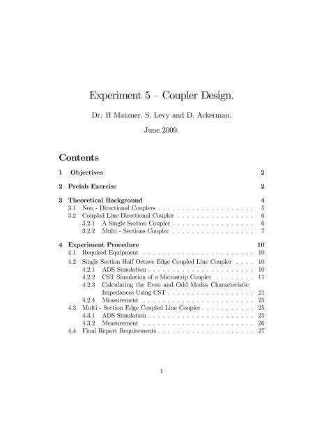
Experiment 5 â Coupler Design.
Experiment 5 â Coupler Design.
Experiment 5 â Coupler Design.

You also want an ePaper? Increase the reach of your titles
YUMPU automatically turns print PDFs into web optimized ePapers that Google loves.
<strong>Experiment</strong>5—<strong>Coupler</strong><strong>Design</strong>.<br />
Dr. H Matzner, S. Levy and D. Ackerman.<br />
June 2009.<br />
Contents<br />
1 Objectives 2<br />
2 Prelab Exercise 2<br />
3 Theoretical Background 4<br />
3.1 Non-Directional<strong>Coupler</strong>s.................... 5<br />
3.2 Coupled Line Directional <strong>Coupler</strong> . . .............. 6<br />
3.2.1 ASingleSection<strong>Coupler</strong>................. 6<br />
3.2.2 Multi-Sections<strong>Coupler</strong>................. 7<br />
4 <strong>Experiment</strong> Procedure 10<br />
4.1 RequiredEquipment ....................... 10<br />
4.2 Single Section Half Octave Edge Coupled Line <strong>Coupler</strong> .... 10<br />
4.2.1 ADSSimulation...................... 10<br />
4.2.2 CSTSimulationofaMicrostrip<strong>Coupler</strong> ........ 11<br />
4.2.3 Calculating the Even and Odd Modes Characteristic<br />
ImpedancesUsingCST.................. 21<br />
4.2.4 Measurement ....................... 25<br />
4.3 Multi-SectionEdgeCoupledLine<strong>Coupler</strong>........... 25<br />
4.3.1 ADSSimulation...................... 25<br />
4.3.2 Measurement ....................... 26<br />
4.4 FinalReportRequirements.................... 27<br />
1
1 Objectives<br />
Upon completion of this study, the student will become familiar with the<br />
following topics:<br />
1. Measuring the basic parameters of couplers.<br />
2. Understanding the role of couplers in a receiver.<br />
2 Prelab Exercise<br />
1. For a 20 dB single section edge coupled line directional coupler, constructed<br />
as a stripline with ground plane, spacing of B =3.2 mm,<br />
dielectric constant of r =4.7, T =0.035 mm, tan δ =0.02, characteristic<br />
impedance of 50 Ω, and center frequency of 1 GHz. Assuming a<br />
lossless component and a perfect termination:<br />
• Write down the S-parameters matrix of the coupler.<br />
• Calculate its Z Oe and Z Oo .<br />
• UseADSLineCalc,setthecomponenttypeto’CPWCPL2’,and<br />
find the dimensions:<br />
W - width of the lines, S - separation of the lines, L -lengthofthe<br />
coupled lines.<br />
2. For a 20 dB single section edge coupled line directional coupler, constructed<br />
as a microstrip, height of substrate hs =1.6 mm, dielectric<br />
constant of r =4.7, T =0.035 mm, tan δ =0.02, characteristic impedance<br />
of 50 Ω, and center frequency of 1 GHz. Assuming a lossless<br />
component and a perfect termination:<br />
• UseADSLineCalc,setthecomponenttypeto’MCLIN’,C_DB =<br />
−20, E_Eff =90 deg,andfind the dimensions:<br />
W - width of the lines, S - separation of the lines, l - length of the coupled<br />
lines (Z Oe and Z Oo remain the same as the previous question).<br />
2
3. For a 20 dB three sections edge coupled line directional coupler, constructed<br />
as a stripline with ground plane, spacing of B =3.2 mm,<br />
dielectric constant of r =4.7, T =0.035 mm, tan δ =0.02, characteristic<br />
impedance of 50 Ω, and center frequency of 1 GHz. Assuming a<br />
lossless component and a perfect termination:<br />
• Calculate Z oe and Z Oo of a edge coupled line with a coupling of<br />
20 dB, center frequency 1 GHz and characteristic impedance of<br />
50 Ω, in a stripline with a ground plane.<br />
• Using ADS LineCalc, find the dimensions:<br />
W - width of the lines, S - separation of the lines, l - length of the coupled<br />
lines, for each section.<br />
3
3 Theoretical Background<br />
A very commonly used basic element in microwave system is the directional<br />
coupler. Its basic function is to sample the forward and reverse travelling<br />
waves through a transmission line or a waveguide. The common use of this<br />
element is to measure the power level of a transmitted or received signal.<br />
The model of a directional coupler is shown in Figure 1.<br />
Forward wave<br />
1 2<br />
Through wave<br />
Sampled wave<br />
4<br />
3<br />
Isolated wave<br />
Figure 1 - Directional coupler model.<br />
As seen in the figure, the coupler is a four-ports device. The forward<br />
travelling wave goes into port 1 and exit from port 2. A small fraction of it<br />
goes out through port 4. In a perfect coupler, no signal appears in port 4.<br />
Since the coupler is a lossless passive element, the sum of the signals power<br />
at ports 1 and 2 equals to the input signal power. The reverse travelling wave<br />
goes into port 2 and out of port 1. A small fraction of it goes out through<br />
port 3. In a perfect coupler, no signal appears in port 4.<br />
The directional coupler S-parameters matrix is:<br />
S =<br />
⎛<br />
⎜<br />
⎝<br />
0 0 −j √ 1 − k 2 k<br />
0 0 k −j √ 1 − k 2<br />
−j √ 1 − k 2 k 0 0<br />
k −j √ 1 − k 2 0 0<br />
⎞<br />
⎟<br />
⎠ (1)<br />
Where k is the coupling factor (a linear value).<br />
One popular realization technique of the directional coupler is the coupledlines<br />
directional coupler; two quarter wavelength line are placed close to each<br />
other. The wave travelling through one line is coupled to the other line. Such<br />
a coupler is shown in Figure 2.<br />
4
Forward wave<br />
1 2<br />
Through wave<br />
Sampled wave<br />
4<br />
3<br />
Isolated wave<br />
Figure 2 - Coupled lines based directional coupler.<br />
Since there is no ideal coupler available, some of the forward travelling<br />
wave is coupled into port 3. This mean that we may think that there is<br />
a reverse travelling wave when there isn’t. This is very critical in application<br />
where the directional coupler is used to measure the return loss of the<br />
device. By calculating 20 log(S 31 /S 41 ) we can find the return loss of the device<br />
connected to port 2. If out coupler has no perfect directivity then out<br />
measurement is not accurate.<br />
There are few simple parameters to describe the functionality of a coupler:<br />
• Insertion Loss: 20 log(S 21 ) or 10 log(1 − k 2 ).<br />
• Return Loss: 20 log(S 11 ).<br />
• Coupling: 20 log(S 31 ) or 20 log(k).<br />
• Directivity: 20 log(S 31 ) − 20 log(S 41 ).<br />
3.1 Non - Directional <strong>Coupler</strong>s<br />
In some applications, the directivity of the coupler is not important. For<br />
instance, if we know there is only forward travelling wave then we may use<br />
a non-directional coupler. One possible realization is using a simple resistor<br />
divider as shown in Figure 3.<br />
5
Z 0<br />
Z 0<br />
Through wave<br />
R 2<br />
Z 0<br />
Sampled wave<br />
R 1<br />
Figure 3 - Resistor divider non-directional coupler.<br />
The transmission lines are not electromagnetically coupled and the coupling<br />
equations are derived from the lumped circuit calculation of the resistor<br />
divider.<br />
3.2 Coupled Line Directional <strong>Coupler</strong><br />
3.2.1 A Single Section <strong>Coupler</strong><br />
There are two modes of current flow in an electromagnetic situation. The first<br />
is one current flowing down one conductor with a contra-flow current back<br />
up the other conductor caused by displacement current coupling between<br />
the two conductors. This is termed the ’odd mode’ current, and it has an<br />
associated odd mode characteristic impedance, styled Z 0o .<br />
Theothermodeisonecurrentflows by displacement current between<br />
each center conductor carrying the same polarity, and the ground that is<br />
common between them. Hence this is called the ’even mode’ current, and it<br />
has an associated even mode characteristic impedance, styled Z 0e .Figure4<br />
shows the polarity of the lines of each mode.<br />
For a single section coupler the even and odd mode characteristic impedances<br />
are defined as:<br />
6
1+C<br />
Z 0e = Z 0<br />
1 − C , (2)<br />
r<br />
1 − C<br />
Z 0o = Z 0<br />
1+C<br />
Where C
A picture of the dimensions of a stripline coupler is shown in Figure 5.<br />
S<br />
B<br />
W<br />
L<br />
Figure 5 - The dimensions of a stripline coupled line coupler.<br />
A top view of a three sections coupled lines coupler is shown in Figure 6.<br />
Figure 6 - Top view of a three sections microstrip coupled line coupler.<br />
8
Because of the symmetry of the structure, all reflection coefficients will<br />
be identical as well as several transmission coefficients.<br />
9
4 <strong>Experiment</strong> Procedure<br />
4.1 Required Equipment<br />
1. Network analyzer.<br />
2. Type N calibration kit.<br />
3. 50 Ω type N accessory kit.<br />
4. Signal generator.<br />
5. Spectrum analyzer.<br />
6. Power splitter.<br />
7. DC power supply.<br />
4.2 Single Section Half Octave Edge Coupled Line <strong>Coupler</strong><br />
4.2.1 ADS Simulation<br />
1. Simulate a single section edge coupled line with the dimensions you<br />
found in ’Prelab Exercise’ question 1, as shown in Figure 1.<br />
10
SSub<br />
SSUB<br />
SSub1<br />
Er=4.7<br />
Mur=1<br />
B=0.32 cm<br />
T=0.035 mm<br />
Cond=1.0E+50<br />
TanD=0.02<br />
S-PARAMETERS<br />
S_Param<br />
SP1<br />
Start=500 MHz<br />
Stop=1500 MHz<br />
Step=1.0 MHz<br />
Term<br />
Term1<br />
Num=1<br />
Z=50 Ohm<br />
Term<br />
Term4<br />
Num=4<br />
Z=50 Ohm<br />
SCLIN<br />
CLin1<br />
Subst="SSub1"<br />
W=cm<br />
S=cm<br />
L=cm<br />
Term<br />
Term3<br />
Num=3<br />
Z=50 Ohm<br />
Term<br />
Term2<br />
Num=2<br />
Z=50 Ohm<br />
Figure 1 - Single section edge coupled lines coupler.<br />
2. Draw the following graphs:<br />
• Coupling (dB).<br />
• Directivity (dB).<br />
• Insertion Loss (dB).<br />
• VSWR primary and secondary line.<br />
• Frequency sensitivity (of the primary line), frequency range 800 MHz−<br />
1200 MHz. Save the data.<br />
4.2.2 CST Simulation of a Microstrip <strong>Coupler</strong><br />
1. Choose the "<strong>Coupler</strong> (Planar, Microstrip, cpw)" template. When this<br />
template is used, the background material is defined as vacuum, the<br />
units are changed to mm, GHz and nsec, and the boundary conditions<br />
are set to "electric". Furthermore, the mesh settings are changed to<br />
account for the planar structure.<br />
2. Define the parameters, as shown in Table 1.<br />
11
Name Value Description<br />
xg L+30 Ground x dimension<br />
yg S+2*w+30 Ground y dimension<br />
t 0.02 Metal thickness<br />
hs 1.6 Substrate thickness<br />
er 4.7 Permittivity of substrate<br />
w<br />
Width of strip<br />
S<br />
L<br />
Spacing between the lines<br />
Length of coupled lines<br />
Table 1 - Parameters Definition<br />
For the missing values, use the dimensions you found in ’Prelab Exercise’<br />
question 2.<br />
3. Create the substrate break, as shown in Figure 2.<br />
Figure 2 - Building the substrate with a new material.<br />
4. Define the first strip, as shown in Figure 3.<br />
12
Figure 3 - Defining the first strip.<br />
5. Zoom in to the end of the strip, as shown in Figure 4.<br />
13
Figure 4 - Zooming in to the end of the strip.<br />
6. Pick the face of the end of the strip, as shown in Figure 5.<br />
14
Figure5-Pickingthefaceoftheendofthestrip.<br />
7. Choose ’Rotate’, press ’ESC’ and then define a rotation axis numerically,<br />
as shown in Figure 6.<br />
Figure 6 - Coordinations of rotation axis.<br />
8. Choose ’Rotate’ again and define the curved edge of the line, as shown<br />
in Figure 7.<br />
15
Figure 7 - Defining the curved edge of the line.<br />
9. Add another strip, as shown in Figure 8.<br />
Figure 8 - Adding another strip.<br />
16
1. Add the curved edge to the first strip with ’Boolean Add (+)’. Do the<br />
same with the additional strip.<br />
2. Transform the total strip, as shown in Figure 9.<br />
Figure 9 - Transforming the total strip.<br />
3. Mirror it with a mirror plane normal (1, 0, 0), asshowninFigure10.<br />
17
Figure 10 - Mirror the strip.<br />
4. Add the mirrored strip to the original strip.<br />
5. Mirror the new strip with a normal plane normal (0, 1, 0), asshownin<br />
Figure 11.<br />
18
Figure 11 - Mirroring again the strip.<br />
6. Create four waveguide ports at each end of a strip line to perform the<br />
S-parameters calculation. An example of the first port location definition<br />
is shown in Figure 12.<br />
19
Figure 12 - The firstportlocationdefinition.<br />
7. Set the frequency range’s upper and lower limit to 0.6 GHz and 1.4 GHz,<br />
respectively.<br />
8. Run a simulation using the ’Transient solver’.<br />
9. View the S-parameters results. Save the data.<br />
TheS-parametersshouldlookasinFigure13.<br />
Figure 13 - S parameters of the <strong>Coupler</strong>.<br />
20
4.2.3 Calculating the Even and Odd Modes Characteristic Impedances<br />
Using CST<br />
In this section you will calculate the even and odd mode characteristic impedances<br />
of microstrip coupled lines using a CST model of them. For this<br />
purpose, you will use one port adjusted for multipins.<br />
CST calculate the line impedance as the division of the power to the sum<br />
of the currents heading into the structure square:<br />
Power<br />
Z =<br />
( P Currents in ) 2<br />
ThepowerisgivenastheintegralofthePoyntingvectorovertheport<br />
area and the currents are calculated by integrating the magnetic field in a<br />
small distance around the conductors’ surfaces.<br />
This impedance expression above differs from the commonly used definition:<br />
Z = V , and thus may lead to different results. For even mode the<br />
I<br />
impedance will be Z ≈ 1 · V<br />
V<br />
, and for odd mode it will be Z ≈ 2 · .<br />
2 I I<br />
1. Start a new project, with the same template as before.<br />
2. Define the parameters, as shown in Table 2.<br />
Name Value Description<br />
xg L Ground x dimension<br />
yg (S+2*w)*3 Ground y dimension<br />
t 0.02 Metal thickness<br />
hs 1.6 Substrate thickness<br />
er 4.7 Permittivity of substrate<br />
w<br />
Width of strip<br />
S<br />
L<br />
Spacing between the lines<br />
Length of coupled lines<br />
Table 2 - Parameters Definition<br />
For the missing values, use the dimensions you found in ’Prelab Exercise’<br />
question 2 (the value of L is not important).<br />
3. Construct the ground and the substrate as described in the previous<br />
section. Construct 2 strips on top of the substrate with the width of<br />
21
w, the separation of S and the length of L. Figure 14 display the lines.<br />
Figure 14 - Model of 2 microstrip coupled lines.<br />
4. Define a waveguide port and check the multipin box in the ’Mode setting’,<br />
as shown in Figure 15.<br />
Figure 15 - Defining the multipin port.<br />
22
Press on the ’Define Pins...’ button and define potentials by pressing<br />
’Add...’. Choose the number of the mode as ’1’, the potential as ’Positive’<br />
and the location as ’Picked’, as shown in Figure 16.<br />
Figure 16 - Defining a potential.<br />
Press ’OK’ and select one of the planar port faces. Add another potential,<br />
also positive and pick the other port face. Figure 17 shows the<br />
potentials definition for even mode.<br />
Figure 17 - Even mode definition.<br />
5. After the port definition, press with the right key of the mouse on<br />
’port1’ from the ’Ports’ folder from the navigation tree and tree ’Info..’,<br />
23
asshowninFigure18.<br />
Figure 18 - Port information.<br />
Calculate the port parameters for frequency of 1 GHz. ’Zline’ is the line<br />
impedance and thus is the even mode characteristic impedance.<br />
6. Deletetheportanddefine a new port with the same dimension as before.<br />
Now, define only two potentials, as shown in Figure 19.<br />
24
Figure 19 - Odd mode definition.<br />
7. Calculate the line impedance again.<br />
8. Compare the CST results to the calculated ones.<br />
4.2.4 Measurement<br />
1. Measure the following S parameters : Input VSWR S 11 , output VSWR<br />
S 22 , Coupling S 41 ,DirectivityS 31 −S 41 .Save the data on magnetic<br />
media.<br />
4.3 Multi - Section Edge Coupled Line <strong>Coupler</strong><br />
4.3.1 ADS Simulation<br />
1. Simulate a single section edge coupled line with the dimensions you<br />
found in ’Prelab Exercise’ question 3, as shown in Figure 20.<br />
25
SSub<br />
S-PARAMETERS<br />
SSUB<br />
SSub1<br />
Er=4.7<br />
Mur=1<br />
B=3.2 mm<br />
T=0.035 mm<br />
Cond=1.0E+50<br />
TanD=0.02<br />
S_Param<br />
SP1<br />
Start=500 MHz<br />
Stop=1500 MHz<br />
Step=1.0 MHz<br />
Term<br />
Term4<br />
Num=4<br />
Z=50 Ohm<br />
Term<br />
SCLIN<br />
CLin1<br />
SCLIN<br />
CLin2<br />
SCLIN<br />
CLin3<br />
Term1 Subst="SSub1" Subst="SSub1" Subst="SSub1"<br />
Num=1 W=mm W=mm W=mm<br />
Z=50 Ohm S=mm S=mm S=mm<br />
L=mm L=mm L=mm<br />
Term<br />
Term2<br />
Num=2<br />
Z=50 Ohm<br />
Term<br />
Term3<br />
Num=3<br />
Z=50 Ohm<br />
Figure 20 - Three section edge coupled lines coupler.<br />
4. Draw the following graphs:<br />
• Coupling (dB).<br />
• Directivity (dB).<br />
• Insertion Loss (dB).<br />
• VSWR primary and secondary line.<br />
• Frequency sensitivity (primary line) in the frequency range 800 MHz−<br />
1200 MHz.<br />
Save the data on magnetic media.<br />
4.3.2 Measurement<br />
1. Measure the following S parameters : Input VSWR S 11 , output VSWR<br />
S 22 ,Coupling S 41 and Directivity S 31 −S 41 .Save the data on magnetic<br />
media.<br />
26
4.4 Final Report Requirements<br />
1. Attach all simulation and measurements results.<br />
2. <strong>Design</strong> a three section coupled lines coupler with a Coupling of 20 dB,<br />
center frequency 1 GHz and characteristic impedance of 50 Ω,substrate<br />
FR4 with r =4.2 in a stripline with a ground plane. Find the width,<br />
separation and the length of each section.<br />
Using MATLAB, draw the graphs of the coupling and the directivity of<br />
the coupler in the frequency range 500 MHz - 1500 MHz.<br />
3. Write a MATLAB program that plots the performance of a resistordivider<br />
non-directional coupler as a function of R 2 . Assume Z 0 = R 1 =<br />
50Ω. The parameters to be calculated are:<br />
• Insertion loss.<br />
• Input return loss.<br />
• Coupling.<br />
• Sample port return loss.<br />
References<br />
[1] "Microwave Engineering" David M. Pozar.<br />
27