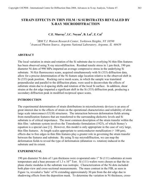
strain effects in thin film / si substrates revealed by x-ray ... - ICDD
strain effects in thin film / si substrates revealed by x-ray ... - ICDD
strain effects in thin film / si substrates revealed by x-ray ... - ICDD

Create successful ePaper yourself
Turn your PDF publications into a flip-book with our unique Google optimized e-Paper software.
Copyright ©JCPDS - International Centre for Diffraction Data 2004, Advances <strong>in</strong> X-<strong>ray</strong> Analy<strong>si</strong>s, Volume 47. 363<br />
STRAIN EFFECTS IN THIN FILM / Si SUBSTRATES REVEALED BY<br />
X-RAY MICRODIFFRACTION<br />
C.E. Mur<strong>ray</strong> 1 , I.C. Noyan 1 , B. Lai 2 , Z. Cai 2<br />
1 IBM T.J. Watson Research Center, Yorktown Heights, NY 10598<br />
2 Avanced Photon Source, Argonne National Laboratory, Argonne, IL 60439<br />
ABSTRACT<br />
The local variation <strong>in</strong> <strong>stra<strong>in</strong></strong> and rotation of the Si substrate due to overly<strong>in</strong>g Ni th<strong>in</strong> <strong>film</strong> features<br />
has been observed us<strong>in</strong>g X-<strong>ray</strong> microdiffraction. Re<strong>si</strong>dual ten<strong>si</strong>le stress <strong>in</strong> 1 µm thick, 190 µm<br />
diameter Ni dots of 990 MPa imparted an average compres<strong>si</strong>ve stress <strong>in</strong> the underly<strong>in</strong>g Si<br />
substrate. Ni Kα fluorescence scans, acquired <strong>si</strong>multaneously with Si (333) diffraction data,<br />
allow for a precise determ<strong>in</strong>ation of the Ni feature edge location relative to the observed shift <strong>in</strong><br />
Si (333) peak po<strong>si</strong>tion. Rock<strong>in</strong>g curve mesh scans, <strong>in</strong> which the sample was translated<br />
perpendicular and parallel to the diffraction plane, were used to deconvolute the <strong>effects</strong> of<br />
substrate <strong>stra<strong>in</strong></strong> due to d-spac<strong>in</strong>g shifts and rotation of the local Si surface. In addition, shear<br />
<strong>stra<strong>in</strong></strong>s at the dot edge imparted a <strong>si</strong>gnificant shift <strong>in</strong> the Si (333) diffraction peak, produc<strong>in</strong>g a<br />
secondary diffraction peak <strong>in</strong> modified reciprocal space scans.<br />
INTRODUCTION<br />
The experimental determ<strong>in</strong>ation of <strong>stra<strong>in</strong></strong> distributions <strong>in</strong> microelectronic devices is an area of<br />
great <strong>in</strong>terest due to the <strong>effects</strong> of <strong>stra<strong>in</strong></strong> on the operational characteristics and reliability of ultralarge<br />
scale <strong>in</strong>terconnect (ULSI) structures. The <strong>in</strong>teraction between deformation fields aris<strong>in</strong>g<br />
from metallization features that are transferred to the surround<strong>in</strong>g dielectric levels and Si<br />
substrate is of critical importance. The most common description of the <strong>stra<strong>in</strong></strong> transfer with<strong>in</strong> the<br />
th<strong>in</strong> <strong>film</strong> / substrate system <strong>in</strong>volves the Timoshenko formulation (1925), of which Stoney’s<br />
equation is a special case [1]. However, this model is only appropriate <strong>in</strong> the case of very large,<br />
th<strong>in</strong> <strong>film</strong> features. At length scales appropriate to semiconductor metallization (< 100 µm),<br />
<strong>effects</strong> due to free edges <strong>in</strong> th<strong>in</strong> <strong>film</strong> features play a greater role <strong>in</strong> govern<strong>in</strong>g the <strong>stra<strong>in</strong></strong> transfer<br />
between the features and substrate. By us<strong>in</strong>g X-<strong>ray</strong> microdiffraction, we can map the<br />
deformation fields to reveal the type of deformation (dilatation vs. rotation) <strong>in</strong>duced <strong>in</strong> the<br />
substrate and its extent.<br />
EXPERIMENTAL<br />
190 µm diameter Ni dots of 1 µm thickness were evaporated onto 1” Si (111) <strong>substrates</strong> at room<br />
temperature and a base pressure of 1.3 x 10 -6 Torr. Si (111) wafers were chosen so that the <strong>in</strong>plane<br />
elastic modulus <strong>in</strong> the substrate was isotropic. Characterization of the Ni dots <strong>in</strong>cluded<br />
both plan-view and cross-sectional measurements. The mass contrast <strong>in</strong> the FIB, as seen <strong>in</strong><br />
Figure 1a, <strong>revealed</strong> a ‘halo’ of Ni extend<strong>in</strong>g approximately 30 µm from the dot edge due to<br />
shadow<strong>in</strong>g <strong>effects</strong> from the depo<strong>si</strong>tion mask. To determ<strong>in</strong>e the variation <strong>in</strong> Ni thickness, cross-
Copyright ©JCPDS - International Centre for Diffraction Data 2004, Advances <strong>in</strong> X-<strong>ray</strong> Analy<strong>si</strong>s, Volume 47. 364<br />
sectional TEM samples were prepared from a section near the dot edge. The cross-sectional<br />
TEM view <strong>in</strong> Figure 1b illustrates the small gra<strong>in</strong> <strong>si</strong>ze of the Ni dot and the profile of the dot<br />
height, which spans from approximately 1 µm through the majority of the dot to 40 nm <strong>in</strong> the<br />
halo region. Although the Ni thickness <strong>in</strong> the halo region was too small to <strong>in</strong>duce stress <strong>in</strong> the Si<br />
substrate, its presence reduced the X-<strong>ray</strong> diffracted <strong>in</strong>ten<strong>si</strong>ty from the substrate due to absorption.<br />
a)<br />
b)<br />
Ni<br />
Si<br />
Figure 1: a) Secondary electron image of a Ni dot depo<strong>si</strong>ted on Si (111) substrate. b) Crosssectional<br />
TEM image near the Ni dot edge of the Ni dot / Si substrate sample. Note that a<br />
protective Pt layer was depo<strong>si</strong>ted over the region of <strong>in</strong>terest prior to TEM sample fabrication.<br />
Measurements were conducted at the Advanced Photon Source at Argonne National Laboratory.<br />
The hard X-<strong>ray</strong> microdiffraction apparatus at the 2ID-D beaml<strong>in</strong>e was used for the<br />
measurements [2]. A s<strong>in</strong>gle crystal monochromator was employed to produce a beam with<br />
energy 8.5 keV and zone plate optics were used to focus the beam to a nom<strong>in</strong>al spot <strong>si</strong>ze of<br />
approximately 0.3 µm. A vertical kappa diffractometer was used <strong>in</strong> which a Si (001) analyzer<br />
crystal was placed between the sample and the Bicron detector to reduce the beam divergence.<br />
An X-<strong>ray</strong> fluorescence detector was used so that X-<strong>ray</strong> diffraction and fluorescence could be<br />
<strong>si</strong>multaneously measured. The Ni Kα fluorescence was monitored so that the beam location<br />
with respect to the th<strong>in</strong> <strong>film</strong> feature was known at all times. Rock<strong>in</strong>g curves were obta<strong>in</strong>ed as the<br />
beam location translated across the Ni dot to produce a map of Si (333) <strong>in</strong>ten<strong>si</strong>ty as a function of<br />
po<strong>si</strong>tion. Maps of Si (333) <strong>in</strong>ten<strong>si</strong>ty were collected as both the angle of the sample (θ) and the<br />
detector (2θ) were varied to produce modified reciprocal space mesh scans at selected po<strong>si</strong>tions<br />
near and <strong>in</strong><strong>si</strong>de the Ni dot edges.<br />
RESULTS<br />
Areal scans of Si (333) rock<strong>in</strong>g curves vs. sample translation were obta<strong>in</strong>ed <strong>by</strong> vary<strong>in</strong>g the beam<br />
po<strong>si</strong>tion <strong>in</strong> one of two perpendicular directions. The first geometry, as illustrated <strong>in</strong> Figure 2a,<br />
<strong>in</strong>volved mov<strong>in</strong>g the sample <strong>in</strong> a direction normal to the diffraction plane, that which conta<strong>in</strong>s<br />
the <strong>in</strong>cident X-<strong>ray</strong> beam (S 0 ) and the diffraction vector (k). Si (333) diffracted <strong>in</strong>ten<strong>si</strong>ty was<br />
collected from rock<strong>in</strong>g curves as a function of po<strong>si</strong>tion. To quantify the shift <strong>in</strong> Si (333) peak
Copyright ©JCPDS - International Centre for Diffraction Data 2004, Advances <strong>in</strong> X-<strong>ray</strong> Analy<strong>si</strong>s, Volume 47. 365<br />
a) b)<br />
Diffraction<br />
plane<br />
45.782<br />
45.780<br />
Si<br />
Ni<br />
k<br />
S 0<br />
θ fit [deg]<br />
45.778<br />
45.776<br />
Scann<strong>in</strong>g<br />
direction<br />
45.774<br />
45.772<br />
-200 -100 0 100 200<br />
Distance from dot center [µm]<br />
Figure 2: a) Diffraction geometry used to collect rock<strong>in</strong>g curves of the Si (333) <strong>in</strong>ten<strong>si</strong>ty across<br />
the Ni dot feature. Scann<strong>in</strong>g direction was normal to the diffraction plane, def<strong>in</strong>ed <strong>by</strong> the<br />
<strong>in</strong>cident X-<strong>ray</strong> beam (S 0 ) and the diffraction vector (k). b) Fitted Si (333) peak center vs.<br />
po<strong>si</strong>tion across Ni dot.<br />
po<strong>si</strong>tion as the beam traversed the Ni dot, diffraction profiles from each of the rock<strong>in</strong>g curves<br />
were fit to Gaus<strong>si</strong>an curves. The fitted peak centers are plotted <strong>in</strong> Figure 2b as a function of<br />
po<strong>si</strong>tion from the dot center. The shift <strong>in</strong> peak po<strong>si</strong>tion is symmetric with respect to the dot<br />
center, <strong>in</strong>dicat<strong>in</strong>g that the shift is due to the change <strong>in</strong> d-spac<strong>in</strong>g <strong>in</strong> the Si lattice. Any <strong>effects</strong> due<br />
to the rotation of the Si lattice should tilt the diffraction vector out of the diffraction plane,<br />
depicted <strong>in</strong> Figure 2a, and would not be captured <strong>in</strong> diffraction <strong>in</strong>formation obta<strong>in</strong>ed from scans<br />
<strong>in</strong> which the rock<strong>in</strong>g angle axis is normal to the diffraction plane.<br />
a) Diffraction<br />
b)<br />
plane<br />
k<br />
Si<br />
Ni<br />
S 0<br />
∆θ fit [deg]<br />
0.006<br />
0.004<br />
0.002<br />
0.000<br />
-0.002<br />
Scann<strong>in</strong>g<br />
direction<br />
-0.004<br />
-0.006<br />
-200 -100 0 100 200<br />
Distance from dot center [µm]<br />
Figure 3: a) Additional diffraction geometry used to collect rock<strong>in</strong>g curves of the Si (333)<br />
<strong>in</strong>ten<strong>si</strong>ty. Scann<strong>in</strong>g direction was parallel to the diffraction plane. b) Shift <strong>in</strong> Si (333) peak<br />
center vs. po<strong>si</strong>tion after deconvolut<strong>in</strong>g the shift due to d-spac<strong>in</strong>g change <strong>in</strong> Figure 2b.
Copyright ©JCPDS - International Centre for Diffraction Data 2004, Advances <strong>in</strong> X-<strong>ray</strong> Analy<strong>si</strong>s, Volume 47. 366<br />
In contrast, the geometry illustrated <strong>in</strong> Figure 3a, <strong>in</strong> which the direction of the sample motion is<br />
parallel to the diffraction plane, produced Si (333) diffracted <strong>in</strong>ten<strong>si</strong>ty profiles that are no longer<br />
symmetric with respect to the Ni dot center. The rock<strong>in</strong>g curves obta<strong>in</strong>ed us<strong>in</strong>g this geometry<br />
captured the <strong>effects</strong> due to the shift <strong>in</strong> d-spac<strong>in</strong>g as well as the rotation of the Si lattice vector. In<br />
order to extract the Si lattice rotation <strong>in</strong>formation, it was necessary to first deconvolute the peak<br />
shift due to the change <strong>in</strong> d-spac<strong>in</strong>g, shown <strong>in</strong> Figure 2b. The result<strong>in</strong>g distribution of the shift <strong>in</strong><br />
the peak centers, plotted <strong>in</strong> Figure 3b, corresponds to an antisymmetric distribution of Si lattice<br />
orientation with respect to the dot center.<br />
a)<br />
b)<br />
+θ<br />
Ni<br />
Si<br />
+ θ<br />
- θ<br />
Figure 4: a) Schematic depiction of the rotation of Si surface lattice vectors due to overly<strong>in</strong>g Ni<br />
dot <strong>in</strong> ten<strong>si</strong>on and b) expected shift <strong>in</strong> θ po<strong>si</strong>tion of the Si (333) peak from the substrate normal.<br />
X-<strong>ray</strong> d vs. s<strong>in</strong> 2 (ψ) analy<strong>si</strong>s <strong>revealed</strong> that the Ni dots were under approximately 990 MPa of<br />
ten<strong>si</strong>le stress. Elastic theory for the bend<strong>in</strong>g of plates [3] prescribes that the Si substrate<br />
underneath the dot would be <strong>in</strong> a state of compres<strong>si</strong>on where the Si lattice planes would be<br />
rotated <strong>in</strong>ward towards the dot center, schematically drawn <strong>in</strong> Figure 4a. As the po<strong>si</strong>tion of the<br />
2θ<br />
θ<br />
Si<br />
Ni<br />
Figure 5: Modified reciprocal space mesh scans (θ vs. 2θ) <strong>in</strong> the bare Si, away from the <strong>effects</strong><br />
of the overly<strong>in</strong>g Ni dot, and those near the Ni dot edge.
Copyright ©JCPDS - International Centre for Diffraction Data 2004, Advances <strong>in</strong> X-<strong>ray</strong> Analy<strong>si</strong>s, Volume 47. 367<br />
beam moves across the sample, the tilt angle (θ) needed to rock the diffracted beam <strong>in</strong>to the<br />
Bragg condition is depicted <strong>in</strong> Figure 4b. This figure corresponds well to the measured peak<br />
shift distribution from Figure 3b and is con<strong>si</strong>stent with the Si lattice vectors be<strong>in</strong>g tilted <strong>in</strong>wards<br />
toward the dot center.<br />
Figure 5 conta<strong>in</strong>s modified reciprocal space scans of Si (333) <strong>in</strong>ten<strong>si</strong>ty conta<strong>in</strong>s the Si (333)<br />
diffracted <strong>in</strong>ten<strong>si</strong>ty as a function of θ and 2θ at 3 locations from the Si substrate. The left-most<br />
scan, which is taken from the bare Si surface, displays the footpr<strong>in</strong>t of the beam as a s<strong>in</strong>gle strip<br />
with two maxima due to the beam stop. A secondary strip of diffracted <strong>in</strong>ten<strong>si</strong>ty appears <strong>in</strong> the<br />
Si (333) modified reciprocal space mesh scans near the dot edge and underneath the dot where<br />
the shear <strong>stra<strong>in</strong></strong> is maximized. Because Pendellösung fr<strong>in</strong>ges appeared between the primary and<br />
secondary diffraction peaks, it is believed that the <strong>effects</strong> of lattice tilt are be<strong>in</strong>g observed from<br />
dynamical diffraction <strong>effects</strong> between the Si lattice planes near the Ni dot and those deeper <strong>in</strong> the<br />
substrate. This effect is currently be<strong>in</strong>g <strong>in</strong>vestigated us<strong>in</strong>g dynamic diffraction <strong>si</strong>mulations <strong>in</strong><br />
which a <strong>stra<strong>in</strong></strong> gradient through the substrate thickness is present.<br />
SUMMARY<br />
The <strong>effects</strong> of <strong>stra<strong>in</strong></strong> <strong>in</strong> Si <strong>substrates</strong> due to overly<strong>in</strong>g th<strong>in</strong> <strong>film</strong> features can be detected us<strong>in</strong>g X-<br />
<strong>ray</strong> microdiffraction. By analyz<strong>in</strong>g both the diffracted peak po<strong>si</strong>tion and <strong>in</strong>tegrated <strong>in</strong>ten<strong>si</strong>ty, one<br />
can determ<strong>in</strong>e the extent and magnitude of the <strong>stra<strong>in</strong></strong> fields. The variation <strong>in</strong> peak po<strong>si</strong>tion<br />
details the rotation and d-spac<strong>in</strong>g shift <strong>in</strong> the Si lattice due to k<strong>in</strong>ematic diffraction <strong>effects</strong>. The<br />
shift <strong>in</strong> peak po<strong>si</strong>tion is most pronounced underneath the Ni dot edges. Rock<strong>in</strong>g curve mesh<br />
scans <strong>in</strong> which the sample was translated perpendicular to the diffraction plane were used to<br />
deconvolute the <strong>effects</strong> of substrate <strong>stra<strong>in</strong></strong> due to d-spac<strong>in</strong>g shifts. The rock<strong>in</strong>g curve mesh scans<br />
obta<strong>in</strong>ed parallel to the diffraction plane reveal an antisymmetric profile <strong>in</strong> the shift of peak<br />
po<strong>si</strong>tion across the Ni dot <strong>in</strong> which the local Si surface normal vectors are tilted <strong>in</strong>ward towards<br />
the dot center. These results are con<strong>si</strong>stent with the predicted behavior <strong>in</strong> the Si surface from<br />
beam and plate bend<strong>in</strong>g theory given an overly<strong>in</strong>g Ni dot <strong>in</strong> ten<strong>si</strong>on.<br />
ACKNOWLEDGMENTS<br />
The authors would like to thank S.J. Chey for sample fabrication, C.C. Goldsmith for the X-<strong>ray</strong><br />
stress measurements and H. Yan for dynamical diffraction work. Work at the Advanced Photon<br />
Source was supported <strong>by</strong> the U.S. Dept. of Energy, Office of Science, Ba<strong>si</strong>c Energy Sciences,<br />
under Contract No. W-31-109-Eng-38.<br />
REFERENCES<br />
[1] S. Timoshenko, J. Opt. Soc. Am. 11, 233 (1925)<br />
[2] J. Libera, Z. Cai, B. Lai and S. Xu, Rev. Sci. Instrum. 73, 1506 (2002)<br />
[3] S. Timoshenko and S. Wo<strong>in</strong>osky-Krieger, Theory of Plates and Shells, 2 nd Ed. (McGraw-<br />
Hill, New York, 1959)