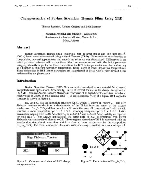
Characterization of Barium Strontium Titanate Films Using XRD - ICDD
Characterization of Barium Strontium Titanate Films Using XRD - ICDD
Characterization of Barium Strontium Titanate Films Using XRD - ICDD

You also want an ePaper? Increase the reach of your titles
YUMPU automatically turns print PDFs into web optimized ePapers that Google loves.
Copyright (C) JCPDS-International Centre for Diffraction Data 1999<br />
38<br />
<strong>Characterization</strong> <strong>of</strong> <strong>Barium</strong> <strong>Strontium</strong> <strong>Titanate</strong> <strong>Films</strong> <strong>Using</strong> <strong>XRD</strong><br />
Abstract<br />
Thomas Remmel, Richard Gregory and Beth Baumert<br />
Materials Research and Strategic Technologies<br />
Semiconductor Products Sector, Motorola Inc.<br />
Mesa, Arizona<br />
<strong>Barium</strong> <strong>Strontium</strong> <strong>Titanate</strong> (BST) materials, both in target (bulk) and thin film (6OOA-<br />
12OOA) form, were characterized using x-ray diffraction (<strong>XRD</strong>). Film structure as a function <strong>of</strong><br />
composition, processing parameters and underlying substrate was determined. Differences in the<br />
lattice parameter between bulk and sputtered film form were observed, with the lattice parameter<br />
being significantly larger for the films. In addition, the BST lattice parameter was observed to vary<br />
as a function <strong>of</strong> thin film deposition temperature, being larger at lower deposition temperatures.<br />
These differences in BST lattice parameters are investigated in detail with a view toward better<br />
understanding the phenomena.<br />
Introduction<br />
<strong>Barium</strong> <strong>Strontium</strong> <strong>Titanate</strong> (BST) films are under investigation as a material for advanced<br />
integrated circuit applications. Specifically, BST is <strong>of</strong> interest for use as the charge storage cell in<br />
DRAMS (Dynamic Access Random Memories)“” because <strong>of</strong> its high dielectric constant, which can<br />
reach values <strong>of</strong> 20000 in bulk ceramic B ST’ ‘. A cross-sectional view <strong>of</strong> a typical BST capacitor<br />
structure is shown in Figure 1.<br />
Ba,+Sr,TiO, has the perovskite structure ABX, which is shown in Figure 2. The high<br />
dielectric constant results from a displacement <strong>of</strong> the Ti ion from the center <strong>of</strong> the oxygen<br />
octahedron. Ba,-,Sr,TiO, exhibits complete solid solubility over all compositions12, with a cubic<br />
structure at room temperature for 0.3 I x I 1, becoming tetragonal for 0 I x I 0.3. Lattice<br />
parameters ranging from 3.905 A for SrTiO, to a=3.994 A and c=4.038 A for BaTiO, are reported<br />
for bulk BST . For DRAM applications, the cubic form <strong>of</strong> BST is preferred, with higher<br />
dielectric constants attained close to x=0.3. The tetragonal distortion <strong>of</strong> BST is associated with the<br />
paraelectric-to-ferroelectric transition, which is close to room temperature for the composition<br />
Bao,7Sro,3Ti0,. The Curie temperature decreases with increasing Sr content, as shown in Figure 3.<br />
Figure 1. Cross-sectional view <strong>of</strong> BST charge<br />
storage capacitor<br />
Figure 2. The structure <strong>of</strong> Ba,Sr,TiO,.
Copyright (C) JCPDS-International Centre for Diffraction Data 1999<br />
39<br />
Experimental<br />
BST films were characterized<br />
using a full arsenal <strong>of</strong> analytical<br />
techniques. This paper focuses on the<br />
results <strong>of</strong> <strong>XRD</strong> analysis. All<br />
diffraction data reported here were<br />
obtained with a Rigaku rotating anode,<br />
CuKa source, using Bragg-Brentano<br />
geometry. Operating conditions were<br />
typically 50kV, 2OOmA.<br />
BST Target<br />
Analysis<br />
0 02 0.4 06 OS 1.0<br />
BaTiQ<br />
SrTi03<br />
x (SrTiO3) ---+<br />
Figure 3. Curie temperature <strong>of</strong> Ba,.,Sr,TiO, as a<br />
function <strong>of</strong> stoichiometry.<br />
Several BST sputter targets were characterized via <strong>XRD</strong> to determine structure and<br />
uniformity. Shown in Figure 4 is the <strong>XRD</strong> pattern <strong>of</strong> a Bao,sSro,,TiO, target from supplier A. The<br />
target appears to be comprised <strong>of</strong> a single phase <strong>of</strong> BST. As seen in the higher order peaks, the<br />
peak positions corresponds very closely with the those expected for the nominal stoichiometry.<br />
From the <strong>XRD</strong> pattern, the stoichiometry was estimated to be Ba,,,,Sr,,,,TiO,, which agreed very<br />
well with chemical analyses.<br />
- 5<br />
cd<br />
2-a<br />
.$=<br />
2<br />
3<br />
c<br />
k?<br />
p;?;<br />
x<br />
2<br />
9<br />
.z<br />
x<br />
2<br />
B<br />
3<br />
i2<br />
2<br />
k<br />
74 76 78 82 84 86<br />
20 50 60<br />
2-Theta<br />
Figure 4. <strong>XRD</strong> pattern <strong>of</strong> Ba,,$r,.,TiO, target from supplier A.
Copyright (C) JCPDS-International Centre for Diffraction Data 1999<br />
40<br />
On the other hand, <strong>XRD</strong> analysis <strong>of</strong> another target from supplier B, shown in Figure 5,<br />
reveals a mixture <strong>of</strong> BST phases, including the nominal Ba,,,Sr,,TiO,, along with traces <strong>of</strong><br />
BaTiO, (BTO) and SrTiO, (STO). The existence <strong>of</strong> the secondary phases <strong>of</strong> BTO and ST0 is<br />
evidenced by the shoulders at the base <strong>of</strong> the peaks.<br />
- 3<br />
cd<br />
h<br />
.s<br />
8<br />
%<br />
22<br />
!&<br />
b4<br />
2<br />
9<br />
.s<br />
x<br />
2<br />
2<br />
2<br />
e:<br />
A<br />
I 74 76 78 80 82 84 86<br />
2-Theta<br />
(111)<br />
(200)<br />
(211)<br />
(100)<br />
I h I<br />
(220)<br />
/n, I\\ (3 10) (222)<br />
20 30 40 50 60<br />
2-Theta<br />
70 80 90<br />
Figure 5. <strong>XRD</strong> pattern <strong>of</strong> Bao,$ro,5Ti0, target from supplier B.<br />
to consist <strong>of</strong> a mixture <strong>of</strong> BST, BTO and ST0 phases.<br />
This target was found<br />
BST Film<br />
Analysis<br />
BST films <strong>of</strong> various compositions<br />
were deposited by MOD<br />
Decomposition)/spin-on<br />
(Metal-Organic<br />
techniques,<br />
MOCVD (Metal-Organic Chemical Vapor<br />
Deposition) and RF magnetron sputtering<br />
2<br />
0<br />
onto (100) Si substrates. Shown in Figure ‘g<br />
6 are the diffraction scans from a series <strong>of</strong> 2<br />
nominal 2000A thick sol-gel/spin-on 2<br />
Ba,Sr,TiO, films. A shift in the 2-theta<br />
peak positions as a function <strong>of</strong> BST film 2<br />
composition is apparent in these scans.<br />
Comparison <strong>of</strong> the lattice parameter<br />
calculated from the spin-on films with those<br />
reported in the literatureI for bulk BST 20 25 30 35 40 45 50 55 60<br />
2 theta<br />
indicates reasonable agreement, as shown<br />
Figure 6. <strong>XRD</strong> patterns <strong>of</strong> spin-on Ba,Sr,TiO,<br />
films for x= 0 to 1.0.
Copyright (C) JCPDS-International Centre for Diffraction Data 1999<br />
41<br />
in Figure 7. Similarly, analysis <strong>of</strong><br />
MOCVD films <strong>of</strong> Ba,,Sr,,TiO, yielded<br />
lattice parameters similar to those <strong>of</strong> the<br />
bulk material. However, review <strong>of</strong> the<br />
literature’3-‘5 and in-house analysis <strong>of</strong><br />
sputtered Ba,-,Sr,TiO, films indicates lattice<br />
parameters much larger than those expected<br />
for bulk material. This anomaly for<br />
sputtered BST films has been reported by<br />
other investigators and has been explained<br />
as being due to “nonequilibrium, highly<br />
distorted states” within the films13. Shown<br />
in Figure 7 is a summary <strong>of</strong> literature and<br />
in-house measurements <strong>of</strong> lattice parameter<br />
as a function <strong>of</strong> stoichiometry for<br />
Ba,-,Sr,TiO,. Note that the sputtered BST<br />
films were deposited at 55O”C, on a variety<br />
<strong>of</strong> crystalline subsbrates, and va@ed in<br />
thickness from 600A to over 3000A. The<br />
films were polycrystalline and typically<br />
randomly oriented.<br />
<strong>XRD</strong> scans <strong>of</strong> sputtered deposited,<br />
6OOA thick Ba,,Sr,,TiO, films as a<br />
function <strong>of</strong> deposition temperature are<br />
shown in Figure 8. These films were<br />
deposited on Pt which had been sputter<br />
deposited on oxidized Si wafers.<br />
Improvement in the degree <strong>of</strong> BST film<br />
crystallinity as deposition temperature is<br />
increased is evident. (Also apparent is the<br />
high degree <strong>of</strong> preferred orientation <strong>of</strong> the<br />
underlying Pt film). A shift in the BST<br />
peak positions toward higher two-theta<br />
angles with increasing deposition<br />
temperature can be seen in the diffraction<br />
scans.<br />
Lattice parameters (in the growth<br />
direction) for the BST films shown in Figure<br />
8 were calculated from the peak positions<br />
(assuming a cubic structure) and are plotted<br />
in Figure 9 as a function <strong>of</strong> deposition<br />
temperature. Results from similar analysis<br />
<strong>of</strong> Ba,,Sr0,,Ti03 films deposited at various<br />
temperatures directly onto SiO, are also<br />
shown in Figure 9. Note that the lattice<br />
parameter for BST films deposited on SiO, is<br />
larger than for those deposited on either Pt or<br />
Ir. This was unexpected but might be<br />
explained by the differences in the degree <strong>of</strong><br />
constraint placed upon the BST lattice by the<br />
substrate. SiO,, being amorphous, would<br />
likely place less constraint compared to the<br />
crystalline Pt or Ir (whose structures are<br />
z<br />
4.10<br />
4.05<br />
5<br />
': 4.00<br />
g<br />
V<br />
.r 8<br />
cl 9 3.95<br />
3.90<br />
Figure 7. Ba,$r,TiO, lattice parameters vs.<br />
composition, taken from the literature and this<br />
work.<br />
20 25 30 35 40 45 50 55 60<br />
%:-theta<br />
Figure 8. <strong>XRD</strong> patterns <strong>of</strong> Ba,,Sr,,TiO,<br />
films deposited at various temperatures on Pt.<br />
4.10 F-<br />
4.08 1<br />
3 4.06 -<br />
3<br />
2 4.04 -<br />
E<br />
g 4.02 -<br />
8<br />
‘g 4.00 -<br />
0<br />
I ” ” 1’3 7 ’ I’, ” I ” I “‘I I ” ” II 7<br />
n 0<br />
v<br />
n<br />
0<br />
v<br />
n<br />
0 O<br />
cl t i<br />
3.98<br />
t Bulk Value = 3.95A 1<br />
3.96 t.,,.l,,‘,l,“,I,‘,,l,,,,I.,,,‘,,,,’..,,’<br />
300 350 400 450 500 550 600 6.50 700<br />
BST Deposition Temperature (“C)<br />
Figure 9. Ba,,,Sr,,TiO, lattice0 parameters vs<br />
deposition temperature for 600A BST films on<br />
various substrates.<br />
n
Copyright (C) JCPDS-International Centre for Diffraction Data 1999<br />
42<br />
cubic and whose lattice parameters are<br />
slightly smaller than BST).<br />
Results from measurement <strong>of</strong> the<br />
FWHM <strong>of</strong> the (110) and (200) peaks for<br />
the same Ba0,,Sr0,,Ti03 films as a function<br />
<strong>of</strong> sputter deposition temperature are shown<br />
in Figure 10. Data for the (110) peak are<br />
shown for Ba&iq,,TiO, deposited on both<br />
Pt and SiO,, whereas only (200) data is<br />
shown for BST on SiO,, due to<br />
interference between the BST (200) and Pt<br />
(200) peaks.<br />
Decreasing ( 110) and (200) peak<br />
widths with increasing deposition<br />
temperature are indicative <strong>of</strong> increased grain<br />
size in the BST films. However the finding<br />
that the (200) BST peaks are about three<br />
times wider than the (110) peaks was<br />
unexpected. The increased Peak<br />
broadening may be indicative <strong>of</strong> distortion<br />
in the lattice (due to defectivity), or the<br />
existence <strong>of</strong> a second phase. Argon is<br />
known to be incorporated into these films<br />
during sputter deposition (this was verified<br />
using Rutherford Backscattering). It is<br />
speculated that excess oxygen, due a<br />
similar mechanism <strong>of</strong> neutral ion<br />
bombardment, may also be incorporated<br />
into these films. Finally, oxygen vacancies<br />
might explain the lattice distortion.<br />
The effect <strong>of</strong> post sputter-deposition<br />
anneal on sputtered BST films is shown in<br />
Figure 11. Ba,,,,Sr,~,,TiO, films, 500A<br />
thick, that had been deposited on SiO,,<br />
were annealed in air for 30 minutes at<br />
temperatures ranging from 650°C to 950°C.<br />
The lattice parameter <strong>of</strong> the BST films<br />
0.8 I<br />
t! I I I I<br />
300 400 500 600<br />
BST Deposition Temperature (“C)<br />
o<br />
(200) BSTLSi02<br />
-! i 2.0<br />
Figure 10. (110) and (200) FWHM for sputtered<br />
Ba,,,Sr,,,TiO, films on SiO, and Pt.<br />
4.00 , , , , , , , , , , , , , . 0.7<br />
\<br />
2 3.98 -<br />
3<br />
8<br />
I2 3.96 -<br />
8<br />
.a<br />
3 3.94 -<br />
\<br />
\ ‘%<br />
\ \<br />
\<br />
‘*<br />
\<br />
‘&<br />
’ ‘\<br />
\ * ‘1 \ \ ‘0<br />
\ ’<br />
‘,@ ‘\<br />
\ \ k<br />
\ \<br />
l ’<br />
1<br />
- 0.6 -<br />
z<br />
- 0.5 2<br />
9<br />
- 0.4 2<br />
B<br />
\ 2<br />
- 0.3 -<br />
3.92 I.
Copyright (C) JCPDS-International Centre for Diffraction Data 1999<br />
43<br />
d-i.<br />
20 25 30 3.5 40 45 50 55 60<br />
2 theta<br />
392t,““““““““‘,i<br />
0 500 1000 1500 2000<br />
BST Film Thickness (A)<br />
Figure 12. <strong>XRD</strong> patterns <strong>of</strong> various thickness<br />
Ba,,,Sr,,,TiO, films deposited on Pt.<br />
Figure 13. Ba,,Sr,.,TiO, lattice parameters vs<br />
film thickness for SiO, and Pt underlying<br />
films.<br />
than 200 A appeared to be amorphous. These results are consistent with the constraining effect <strong>of</strong><br />
the substrate, as discussed earlier.<br />
The change in FWHM <strong>of</strong> the (110) peak as a function <strong>of</strong> thickness for Ba&Sr,,,TiO, films<br />
deposited on both Pt and SiO, is shown in Figure 14. The trend <strong>of</strong> decreasing peak width with<br />
increasing film thickness agrees with the rationale that grain size (in the growth direction) increases<br />
with film thickness. Grain sizes, calculated from the (110) peak broadening using the Scherrer<br />
formula16, are on the order <strong>of</strong> the film thickness, but decrease as a percentage <strong>of</strong> film thickness as<br />
the thickness increases.<br />
Sputter deposiied BSOT films appear to be randomly oriented, w$h a hint <strong>of</strong> (110) preferred<br />
orientation in the 400A-600A thick range. Above thicknesses <strong>of</strong> lOOOA, the films begin to exhibit<br />
(111) texturing. With the exception <strong>of</strong> the very early stages <strong>of</strong> film growth, the substrate (Pt, Ir<br />
and Si02) appears to have little effect on the texture <strong>of</strong> the films.<br />
The effect <strong>of</strong> sputtering gas composition on the structure <strong>of</strong> the BST films was also<br />
investigated. Shown in Figure 15 are <strong>XRD</strong> patterns <strong>of</strong> Ba,,,Sr,,TiO, films deposited on SiO,<br />
under various argon:oxygen (Ar:O,) gas<br />
0.60<br />
flow ratios. The thicknes%es <strong>of</strong> these<br />
1”’ 0 ” ” 1 ” 1 ” ” 1 ‘I<br />
films were nominally 600A, with the<br />
exception <strong>of</strong> the lO$l:O Ar:O, film, which<br />
was about 1300 A. Judging from the<br />
positions <strong>of</strong> the (110) peak in Figure 15,<br />
the lattice parameter does not appear to<br />
vary much as a function <strong>of</strong> Ar:O, gas<br />
ratio. However, the diffraction pattern<br />
<strong>of</strong> the thicker, 100:0 Ar:O, film indicates<br />
that the texture <strong>of</strong> these films varies as a<br />
function <strong>of</strong> thickness, as noted<br />
previously.<br />
An interesting feature evident in<br />
the <strong>XRD</strong> pattern <strong>of</strong> the film deposited<br />
with 50:50 Ar:O, gas ratio is the<br />
existence <strong>of</strong> a doublet in the (200) peak.<br />
This <strong>XRD</strong> pattern is shown in more<br />
3<br />
B<br />
0.50<br />
“v N<br />
z 0.40<br />
Ft<br />
G<br />
2 0.30<br />
0.20~““““’<br />
0 5ocl 1000 1500<br />
BST Film Thickness (A)<br />
Figure 14. Ba,$&,,TiO, lattice parameters vs film<br />
thickness for SiO, and Pt underlying films.
Copyright (C) JCPDS-International Centre for Diffraction Data 1999<br />
44<br />
detail in Figure 16, where a doublet is also<br />
seen in the (100) peak. The position <strong>of</strong> the<br />
higher 2-theta (100) and (200) peaks in<br />
these doublets agrees very well with a<br />
lattice parameter <strong>of</strong> 3.95 A, equal to that <strong>of</strong> .g<br />
bulk Ba,,Sr,,,TiO,. The existence <strong>of</strong> the<br />
doublets seems to indicate that either the<br />
sputtered BST film is comprised <strong>of</strong> multiple 2<br />
phases, or the film is not cubic, but exhibits 6<br />
some lattice distortion.<br />
It is possible to fit the diffraction<br />
scan shown in Figure 16 with a tetragonal<br />
structure having elongated a and b<br />
directions, as shown by the stick patterns.<br />
Although the peak positions agree very<br />
well, the (200) and (002) intensities are<br />
reversed from that expected <strong>of</strong> a randomly<br />
oriented, conventional tetragonal structure<br />
where oa. To attain the proper intensity<br />
ratios, either the tetragonal structure is <strong>of</strong><br />
the form where a>c or the BST film is not<br />
fully random in orientation.<br />
20 25 30 35 40 45 50 55 60<br />
2-theta<br />
Figure 15. <strong>XRD</strong> patterns <strong>of</strong> Ba,,,Sr,,TiO, films<br />
deposited using various Ar:02 gas flow ratios<br />
20 25 30 35 40 45 50 55 60<br />
2-theta<br />
Figure 16. Detailed <strong>XRD</strong> pattern for 6OOA Ba,,,Sr,,,TiO, film deposited on SiO, using 50:59<br />
argon:oxygen gas flow ratio. Stick patterns represent positions <strong>of</strong> tetragonal phase <strong>of</strong> a=b=4.06 A<br />
and c=3.95 A.
Copyright (C) JCPDS-International Centre for Diffraction Data 1999<br />
45<br />
Conclusions<br />
<strong>XRD</strong> has proven to be an invaluable tool in the development <strong>of</strong> BST for DRAM<br />
applications. <strong>Characterization</strong> <strong>of</strong> BST films as a function <strong>of</strong> the numerous process parameters has<br />
revealed insight into the structure <strong>of</strong> the films and their dependence upon process conditions.<br />
Sputtered BST films were found to have lattice parameters larger than MOD/spin-on, MOCVD and<br />
bulk BST. This discrepancy was even greater for films sputtered onto SiO,, and was found to<br />
decrease as a function <strong>of</strong> post-deposition anneal. Abnormal width and shape <strong>of</strong> the (200) peak<br />
appears to point toward distortion <strong>of</strong> the BST lattice in sputtered films, perhaps <strong>of</strong> the tetragonal<br />
form.<br />
Referxmces<br />
1. W.Y. Hsu, J.D. Luttmer, R. Tsu, S. Summerfelt, M. Bedekar, T. Tokumoto, and J .<br />
Nulman, Appl. Phys. Lett. 66, 2975 (1995).<br />
2. T. Kawahara, M. Yamamuka, A. Yuuki, and K. Ono, Jpn. J. Appl. Phys. 34, 5077 (1995).<br />
3. K. Takemura, S. Yamamichi, P.-Y. Lesaicherre, K. Tokashiki, H. Miyamoto, H. Ono, Y.<br />
Miyasaka, and M. Yoshida, Jpn. J. Appl. Phys. 34, 5224 (1995).<br />
4. Q.X. Jia, X.D. Wu, S.R. Foltyn, and P. Tiwari, Appl. Phys. Lett. 66, 2 197 (1995).<br />
5. K. Numata, Y. Fukuda, K. Aoki, and A. Nishimura, Jpn. J. Appl. Phys. 34, 5245 (1995).<br />
6. C.S. Hwang, S.O. Park, C.S. Kang, H.-J. Cho, H.-K. Kang, S.T. Ahn, and M.Y. Lee,<br />
Jpn. J. Appl. Phys. 34, 5178 (1995).<br />
7. T. Nakamura, Y. Yamanaka, A. Morimoto, and T. Shimizu, Jpn. J. Appl. Phys. 34, 5150<br />
(1995).<br />
8. K. Abe and S. Komatsu, Jpn. J. Appl. Phys. 33, 5297 (1994).<br />
9. P. Kirlin, S. Bilodeau, and P. van Buskirk, Integrated Ferroelectrics 7, 307 (1995).<br />
10 C-J. Peng and S.B. Krupanidhi, J. Mater. Res. 10, 708 (1995).<br />
11. J.T. Fielding, Jr., S.J. Jang and T.R. Shrout, Proceed. Ninth IEEE Int. Symp. on<br />
Applications <strong>of</strong> Ferroelectrics, 363 (1994).<br />
12. A. Basjamin and R.C. DeVries, J. Am. Ceram. Sot. 40, 373 (1957).<br />
13. T.S. Kim, C.H. Kim and M.H. Oh, J. Appl. Phys. 75, 7998 (1994).<br />
14. K. Fujimoto, Y. Kobayashi, and K. Kubota, Thin Solid <strong>Films</strong>, 169,249 (1989)<br />
15. T. Horikawa, N. Mikami, T. Makita, J. Tanimura, M. Kataoka, K. Sato and M. Nunoshita,<br />
Jpn. J. Appl. Phys, 32, 4126 (1993).<br />
16. B.D. Cullity, p. 102, Elements <strong>of</strong> X-Ray DifSraction, 2nd Ed. (Addison-Wesley Publishing<br />
Co., Inc., 1978).