Introduction to the Altera Nios II Soft Processor - FTP - Altera
Introduction to the Altera Nios II Soft Processor - FTP - Altera
Introduction to the Altera Nios II Soft Processor - FTP - Altera

You also want an ePaper? Increase the reach of your titles
YUMPU automatically turns print PDFs into web optimized ePapers that Google loves.
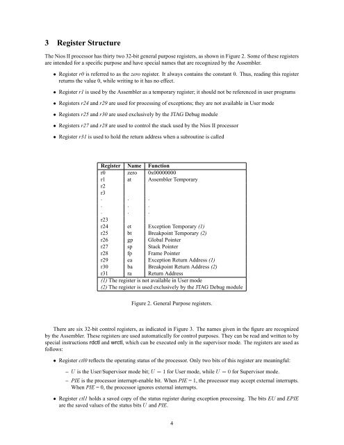
3 Register Structure<br />
The <strong>Nios</strong> <strong>II</strong> processor has thirty two 32-bit general purpose registers, as shown in Figure 2. Some of <strong>the</strong>se registers<br />
are intended for a specific purpose and have special names that are recognized by <strong>the</strong> Assembler.<br />
• Register r0 is referred <strong>to</strong> as <strong>the</strong> zero register. It always contains <strong>the</strong> constant 0. Thus, reading this register<br />
returns <strong>the</strong> value 0, while writing <strong>to</strong> it has no effect.<br />
• Register r1 is used by <strong>the</strong> Assembler as a temporary register; it should not be referenced in user programs<br />
• Registers r24 and r29 are used for processing of exceptions; <strong>the</strong>y are not available in User mode<br />
• Registers r25 and r30 are used exclusively by <strong>the</strong> JTAG Debug module<br />
• Registers r27 and r28 are used <strong>to</strong> control <strong>the</strong> stack used by <strong>the</strong> <strong>Nios</strong> <strong>II</strong> processor<br />
• Register r31 is used <strong>to</strong> hold <strong>the</strong> return address when a subroutine is called<br />
Register Name Function<br />
r0 zero 0x00000000<br />
r1 at Assembler Temporary<br />
r2<br />
r3<br />
· · ·<br />
· · ·<br />
· · ·<br />
r23<br />
r24 et Exception Temporary (1)<br />
r25 bt Breakpoint Temporary (2)<br />
r26 gp Global Pointer<br />
r27 sp Stack Pointer<br />
r28 fp Frame Pointer<br />
r29 ea Exception Return Address (1)<br />
r30 ba Breakpoint Return Address (2)<br />
r31 ra Return Address<br />
(1) The register is not available in User mode<br />
(2) The register is used exclusively by <strong>the</strong> JTAG Debug module<br />
Figure 2. General Purpose registers.<br />
There are six 32-bit control registers, as indicated in Figure 3. The names given in <strong>the</strong> figure are recognized<br />
by <strong>the</strong> Assembler. These registers are used au<strong>to</strong>matically for control purposes. They can be read and written <strong>to</strong> by<br />
special instructions rdctl and wrctl, which can be executed only in <strong>the</strong> supervisor mode. The registers are used as<br />
follows:<br />
• Register ctl0 reflects <strong>the</strong> operating status of <strong>the</strong> processor. Only two bits of this register are meaningful:<br />
– U is <strong>the</strong> User/Supervisor mode bit; U = 1 for User mode, while U = 0 for Supervisor mode.<br />
– PIE is <strong>the</strong> processor interrupt-enable bit. When PIE = 1, <strong>the</strong> processor may accept external interrupts.<br />
When PIE = 0, <strong>the</strong> processor ignores external interrupts.<br />
• Register ctl1 holds a saved copy of <strong>the</strong> status register during exception processing. The bits EU and EPIE<br />
are <strong>the</strong> saved values of <strong>the</strong> status bits U and PIE.<br />
4