Introduction to the Altera Nios II Soft Processor - FTP - Altera
Introduction to the Altera Nios II Soft Processor - FTP - Altera
Introduction to the Altera Nios II Soft Processor - FTP - Altera

You also want an ePaper? Increase the reach of your titles
YUMPU automatically turns print PDFs into web optimized ePapers that Google loves.
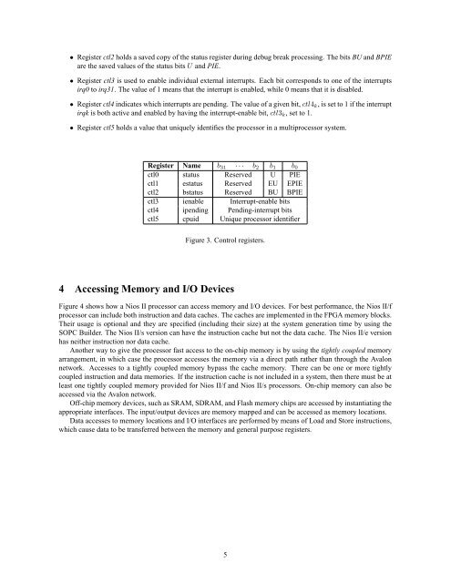
• Register ctl2 holds a saved copy of <strong>the</strong> status register during debug break processing. The bits BU and BPIE<br />
are <strong>the</strong> saved values of <strong>the</strong> status bits U and PIE.<br />
• Register ctl3 is used <strong>to</strong> enable individual external interrupts. Each bit corresponds <strong>to</strong> one of <strong>the</strong> interrupts<br />
irq0 <strong>to</strong> irq31. The value of 1 means that <strong>the</strong> interrupt is enabled, while 0 means that it is disabled.<br />
• Register ctl4 indicates which interrupts are pending. The value of a given bit, ctl4 k , is set <strong>to</strong> 1 if <strong>the</strong> interrupt<br />
irqk is both active and enabled by having <strong>the</strong> interrupt-enable bit, ctl3 k , set <strong>to</strong> 1.<br />
• Register ctl5 holds a value that uniquely identifies <strong>the</strong> processor in a multiprocessor system.<br />
Register Name b 31 · · · b 2 b 1 b 0<br />
ctl0 status Reserved U PIE<br />
ctl1 estatus Reserved EU EPIE<br />
ctl2 bstatus Reserved BU BPIE<br />
ctl3 ienable Interrupt-enable bits<br />
ctl4 ipending Pending-interrupt bits<br />
ctl5 cpuid Unique processor identifier<br />
Figure 3. Control registers.<br />
4 Accessing Memory and I/O Devices<br />
Figure 4 shows how a <strong>Nios</strong> <strong>II</strong> processor can access memory and I/O devices. For best performance, <strong>the</strong> <strong>Nios</strong> <strong>II</strong>/f<br />
processor can include both instruction and data caches. The caches are implemented in <strong>the</strong> FPGA memory blocks.<br />
Their usage is optional and <strong>the</strong>y are specified (including <strong>the</strong>ir size) at <strong>the</strong> system generation time by using <strong>the</strong><br />
SOPC Builder. The <strong>Nios</strong> <strong>II</strong>/s version can have <strong>the</strong> instruction cache but not <strong>the</strong> data cache. The <strong>Nios</strong> <strong>II</strong>/e version<br />
has nei<strong>the</strong>r instruction nor data cache.<br />
Ano<strong>the</strong>r way <strong>to</strong> give <strong>the</strong> processor fast access <strong>to</strong> <strong>the</strong> on-chip memory is by using <strong>the</strong> tightly coupled memory<br />
arrangement, in which case <strong>the</strong> processor accesses <strong>the</strong> memory via a direct path ra<strong>the</strong>r than through <strong>the</strong> Avalon<br />
network. Accesses <strong>to</strong> a tightly coupled memory bypass <strong>the</strong> cache memory. There can be one or more tightly<br />
coupled instruction and data memories. If <strong>the</strong> instruction cache is not included in a system, <strong>the</strong>n <strong>the</strong>re must be at<br />
least one tightly coupled memory provided for <strong>Nios</strong> <strong>II</strong>/f and <strong>Nios</strong> <strong>II</strong>/s processors. On-chip memory can also be<br />
accessed via <strong>the</strong> Avalon network.<br />
Off-chip memory devices, such as SRAM, SDRAM, and Flash memory chips are accessed by instantiating <strong>the</strong><br />
appropriate interfaces. The input/output devices are memory mapped and can be accessed as memory locations.<br />
Data accesses <strong>to</strong> memory locations and I/O interfaces are performed by means of Load and S<strong>to</strong>re instructions,<br />
which cause data <strong>to</strong> be transferred between <strong>the</strong> memory and general purpose registers.<br />
5