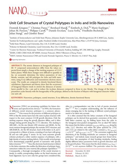
Unit Cell Structure of Crystal Polytypes in InAs and InSb Nanowires
Unit Cell Structure of Crystal Polytypes in InAs and InSb Nanowires
Unit Cell Structure of Crystal Polytypes in InAs and InSb Nanowires

Create successful ePaper yourself
Turn your PDF publications into a flip-book with our unique Google optimized e-Paper software.
LETTER<br />
pubs.acs.org/NanoLett<br />
<strong>Unit</strong> <strong>Cell</strong> <strong>Structure</strong> <strong>of</strong> <strong>Crystal</strong> <strong>Polytypes</strong> <strong>in</strong> <strong>InAs</strong> <strong>and</strong> <strong>InSb</strong> <strong>Nanowires</strong><br />
Dom<strong>in</strong>ik Kriegner,* ,† Christian Panse,* ,‡ Bernhard M<strong>and</strong>l, †,§ Kimberly A. Dick, §,|| Mario Kepl<strong>in</strong>ger, †<br />
Johan M. Persson,^ Philippe Car<strong>of</strong>f, #,§ Daniele Ercolani, z Lucia Sorba, z Friedhelm Bechstedt, ‡<br />
Julian Stangl, † <strong>and</strong> G€unther Bauer †<br />
† Institute <strong>of</strong> Semiconductor <strong>and</strong> Solid State Physics, Johannes Kepler University L<strong>in</strong>z, Altenbergerstrasse 69 A-4040 L<strong>in</strong>z, Austria<br />
‡ Institut f€ur Festk€orpertheorie und -optik, Friedrich-Schiller-Universit€at Jena, Max-Wien-Platz 1, D-07743 Jena, Germany<br />
§ Solid State Physics, Lund University, Box 118, S-22100 Lund, Sweden<br />
^Center<br />
Polymer & Materials Chemistry, Lund University, Box 124, S-22100 Lund, Sweden<br />
for Electron Nanoscopy, Technical University <strong>of</strong> Denmark, Fysikvej, build<strong>in</strong>g 307, DK-2800 Kgs Lyngby, Denmark<br />
)<br />
# IEMN, UMR CNRS 8520, BP 60069, Avenue Po<strong>in</strong>care, 59652 Villeneuve d’Ascq, France<br />
z NEST, Istituto Nanoscienze-CNR <strong>and</strong> Scuola Normale Superiore, Piazza S. Silvestro 12, I-56127 Pisa, Italy<br />
bS Support<strong>in</strong>g Information<br />
ABSTRACT: The atomic distances <strong>in</strong> hexagonal polytypes <strong>of</strong><br />
III V compound semiconductors differ from the values expected<br />
from simply a change <strong>of</strong> the stack<strong>in</strong>g sequence <strong>of</strong> (111)<br />
lattice planes. While these changes were difficult to quantify so<br />
far, we accurately determ<strong>in</strong>e the lattice parameters <strong>of</strong> z<strong>in</strong>c<br />
blende, wurtzite, <strong>and</strong> 4H polytypes for <strong>InAs</strong> <strong>and</strong> <strong>InSb</strong> nanowires,<br />
us<strong>in</strong>g X-ray diffraction <strong>and</strong> transmission electron microscopy.<br />
The results are compared to density functional theory<br />
calculations. Experiment <strong>and</strong> theory show that the occurrence<br />
<strong>of</strong> hexagonal bilayers tends to stretch the distances <strong>of</strong> atomic<br />
layers parallel to the c axis <strong>and</strong> to reduce the <strong>in</strong>-plane distances compared to those <strong>in</strong> z<strong>in</strong>c blende. The change <strong>of</strong> the lattice<br />
parameters scales l<strong>in</strong>early with the hexagonality <strong>of</strong> the polytype, def<strong>in</strong>ed as the fraction <strong>of</strong> bilayers with hexagonal character with<strong>in</strong><br />
one unit cell.<br />
KEYWORDS: <strong>Nanowires</strong>, polytypes, crystal structure, X-ray diffraction, density functional theory<br />
<strong>Nanowires</strong> (NWs) are promis<strong>in</strong>g c<strong>and</strong>idates for future electronic<br />
<strong>and</strong> optoelectronic devices. 1,2 In NWs, the formation<br />
<strong>of</strong> different crystal structure polytypes is a common phenomenon.<br />
3 10 One reason for the presence <strong>of</strong> different polytypes <strong>in</strong><br />
NWs is that the atomic layers have the same <strong>in</strong>-plane structure with<br />
respect to the most common Æ111æB growth directions. Only the<br />
stack<strong>in</strong>g sequence along the growth direction differs, <strong>and</strong> it <strong>of</strong>ten<br />
changes dur<strong>in</strong>g growth along the [111] direction. The stack<strong>in</strong>g is<br />
ABCABC... for the z<strong>in</strong>c blende (ZB) structure <strong>and</strong> ABAB... for the<br />
most common hexagonal polytype, the wurtzite (WZ) structure, <strong>and</strong><br />
ABCBABCB... for the 4H structure. Each <strong>of</strong> the letters A, B, <strong>and</strong> C<br />
corresponds to a bilayer <strong>of</strong> atoms, consist<strong>in</strong>g <strong>of</strong> one layer with group<br />
III<strong>and</strong>onewithgroupVatoms.S<strong>of</strong>ar,mostnanowiregrowth<br />
schemes produced a rather r<strong>and</strong>om sequence <strong>of</strong> polytypes, with a<br />
high density <strong>of</strong> various stack<strong>in</strong>g defects. Only recently several groups<br />
have demonstrated controlled growth <strong>of</strong> nanowires with specific<br />
lattice structure. 3,6,7,11 14 S<strong>in</strong>ce the electronic b<strong>and</strong> structure is l<strong>in</strong>ked<br />
to the lattice structure, this enables the fabrication <strong>of</strong> polytypic heterostructures<br />
with<strong>in</strong> the same material, like polytypic superlattices. 15,16<br />
Consequently, a thorough <strong>in</strong>vestigation <strong>of</strong> the crystal structure is<br />
timely, to enable correspond<strong>in</strong>g studies on the b<strong>and</strong> structure <strong>and</strong><br />
b<strong>and</strong> alignment. Up to now only few groups have considered this,<br />
<strong>of</strong>ten <strong>in</strong> a semiquantitative way due to lack <strong>of</strong> precise structural<br />
data. 4,17 20 For a complete underst<strong>and</strong><strong>in</strong>g, also the <strong>in</strong>fluence <strong>of</strong><br />
stra<strong>in</strong>s emerg<strong>in</strong>g due to the stack<strong>in</strong>g <strong>of</strong> different crystal polytypes<br />
needs to be taken <strong>in</strong>to account.<br />
It is <strong>of</strong>ten assumed that the lattice constants <strong>of</strong> the hexagonal<br />
polytypes can be derived from geometric conversion <strong>of</strong> the cubic<br />
bulk lattice constant, e.g., by shift<strong>in</strong>g layers from the cubic to<br />
the hexagonal close-packed arrangement. For an ideal WZ lattice<br />
this means that the lattice constants c geom,WZ <strong>and</strong> a geom,WZ along the<br />
cubic [111] direction <strong>and</strong> with<strong>in</strong> the plane spanned by [110]<br />
<strong>and</strong> [112] are related to the cubic lattice constant a c via c geom,WZ<br />
= a c (4/3) 1/2 <strong>and</strong> a geom,WZ = a c /2 1/2 . The conversion neglects that<br />
distortions <strong>of</strong> the bond<strong>in</strong>g tetrahedra are common <strong>in</strong> hexagonal<br />
polytypes, 21 <strong>and</strong> <strong>in</strong>deed, many research groups have found deviations<br />
from this assumption <strong>of</strong> ideal bond<strong>in</strong>g tetrahedra, f<strong>in</strong>d<strong>in</strong>g<br />
slightly different lattice parameters both <strong>in</strong> growth direction <strong>and</strong><br />
<strong>in</strong> the growth plane. This means that the ideal relation c WZ /a WZ =<br />
(8/3) 1/2 is not anymore fulfilled. The particular values for the<br />
Received: November 29, 2010<br />
Revised: February 10, 2011<br />
Published: March 24, 2011<br />
r 2011 American Chemical Society 1483 dx.doi.org/10.1021/nl1041512 | Nano Lett. 2011, 11, 1483–1489
Nano Letters<br />
Figure 1. Transmission electron micrograph <strong>of</strong> an <strong>InAs</strong> wire (a) <strong>and</strong> an<br />
<strong>InSb</strong> wire (b) <strong>and</strong> a sketch <strong>of</strong> hexagonal <strong>and</strong> cubic stacked layers (c). In (a) a<br />
part <strong>of</strong> a wire from sample A1, which consists ma<strong>in</strong>ly <strong>of</strong> the WZ structure<br />
with some stack<strong>in</strong>g faults (SF), is shown. In (b) from bottom to top the ZB,<br />
4H, <strong>and</strong> WZ phase <strong>in</strong> a wire from sample E2 is shown. Both images were<br />
recorded <strong>in</strong> [110] zone axis. Panel c shows the different stack<strong>in</strong>g/bond<br />
configuration <strong>of</strong> a cubic <strong>and</strong> a hexagonal bilayer. Whereas the upper group<br />
III atoms (red) are located above the group V (blue) atoms <strong>in</strong> the hexagonal<br />
case, they are located at an rotated position <strong>in</strong> the cubic case.<br />
lattice parameters <strong>of</strong> WZ <strong>InAs</strong> 22 25 differ, however, considerably<br />
between the different studies. The reason for these discrepancies<br />
is most probably that <strong>in</strong> most growth schemes <strong>of</strong> NWs the<br />
result<strong>in</strong>g polytype structure is not well controlled, lead<strong>in</strong>g to<br />
wires with a more or less r<strong>and</strong>om sequence <strong>of</strong> cubic ZB <strong>and</strong><br />
hexagonal WZ segments <strong>and</strong> possibly also with more complex<br />
stack<strong>in</strong>g forms, result<strong>in</strong>g <strong>in</strong> other polytypes like 4H. In addition,<br />
the wires <strong>of</strong>ten conta<strong>in</strong> a high density <strong>of</strong> defects such as stack<strong>in</strong>g<br />
faults <strong>and</strong> tw<strong>in</strong> boundaries. As a result, the <strong>in</strong>dividual segments <strong>of</strong><br />
the wires are <strong>of</strong>ten mutually stra<strong>in</strong>ed, <strong>and</strong> it is difficult or even<br />
impossible to extract the ”true bulk” lattice parameters <strong>of</strong> the<br />
<strong>in</strong>dividual polytypes from measurements <strong>of</strong> such samples.<br />
In this work, we present precise systematic studies <strong>of</strong> the<br />
variations <strong>of</strong> the unit cell parameters <strong>of</strong> <strong>InAs</strong> <strong>and</strong> <strong>InSb</strong> for ZB,<br />
WZ <strong>and</strong> 4H <strong>in</strong> NWs. We employ high-resolution X-ray diffraction<br />
(XRD) on samples with controlled crystal phase <strong>and</strong> compare the<br />
obta<strong>in</strong>ed lattice parameters to results <strong>of</strong> density functional theory<br />
(DFT) calculations. We can show that deviations from the simple<br />
geometric conversion formula <strong>in</strong>deed exist <strong>and</strong> determ<strong>in</strong>e the real<br />
lattice constants for hexagonal polytypes <strong>of</strong> <strong>InAs</strong> <strong>and</strong> <strong>InSb</strong>. To be<br />
able to determ<strong>in</strong>e the lattice constants a <strong>and</strong> c for WZ, <strong>and</strong> other<br />
hexagonal polytypes, NWs with low defect density <strong>and</strong> sufficiently<br />
long s<strong>in</strong>gle phase segments are required. Transmission electron<br />
microscopy (TEM) was used to select suitable samples, s<strong>in</strong>ce the<br />
microscopic arrangement <strong>of</strong> the different crystal phases cannot be<br />
obta<strong>in</strong>ed from the XRD data directly.<br />
The III V bilayers <strong>in</strong> [000.1] [111] direction 26 can have cubic<br />
or hexagonal character depend<strong>in</strong>g on the stack<strong>in</strong>g A, B, or C <strong>of</strong> the<br />
neighbor<strong>in</strong>g layers: In the cubic case, the layers above <strong>and</strong> below the<br />
considered layer are <strong>of</strong> different type, e.g., a B layer has an A <strong>and</strong> a C<br />
layer as neighbors. In the hexagonal case, the neighbor<strong>in</strong>g layers are<br />
<strong>of</strong> the same type, e.g., a B layer has two A layers as neighbors. In the<br />
ZB structure, all bilayers therefore have cubic character as shown <strong>in</strong><br />
Figure 1c. S<strong>in</strong>ce the periodicity <strong>in</strong> [111] direction is reached after<br />
three bilayers, this structure is also termed 3C. In the WZ geometry,<br />
the periodicity amounts to two bilayers with hexagonal character<br />
(Figure 1c), therefore also denoted as 2H. The 4H polytype has a<br />
periodicity <strong>of</strong> four bilayers with mixed character. <strong>Polytypes</strong> with<br />
)<br />
LETTER<br />
even larger unit cells are possible, e.g., 6H with a ABCACBAB-<br />
CACB... stack<strong>in</strong>g sequence. The total number <strong>of</strong> III Vbilayers<strong>in</strong><br />
the unit cell <strong>of</strong> an pH/pC polytype is given by p. Theratio<strong>of</strong>the<br />
number <strong>of</strong> hexagonal stacked bilayers to the total number <strong>of</strong> bilayers<br />
(p) gives the percentage <strong>of</strong> hexagonality, which is 0% for ZB/3C,<br />
33% for 6H, 50% for 4H, <strong>and</strong> 100% for WZ/2H. The results will be<br />
discussed as a function <strong>of</strong> the hexagonality. The atomic structure <strong>and</strong><br />
electronic structure are <strong>in</strong>timately connected <strong>and</strong> mutually <strong>in</strong>fluence<br />
each other. 15,27,28 This self-consistency leads to the actual atomic<br />
positions for a given bilayer stack<strong>in</strong>g <strong>and</strong> hence III Vpolytype<strong>and</strong><br />
is def<strong>in</strong>ed by vanish<strong>in</strong>g Hellmann Feynman forces, 29 the gradients<br />
<strong>of</strong> the total energy <strong>in</strong> DFT calculations with respect to the atomic<br />
positions. As a result, not only the unit cell dimensions a <strong>and</strong> c <strong>of</strong> a<br />
polytype but also the so-called cell <strong>in</strong>ternal parameters can be<br />
calculated. They describe deformations <strong>of</strong> the bond<strong>in</strong>g tetrahedra,<br />
lead<strong>in</strong>g to slight displacements <strong>of</strong> the atom positions with<strong>in</strong> the unit<br />
cell. S<strong>in</strong>ce theory reveals the reasons <strong>of</strong> geometrical variations, a<br />
comparison with numerical data contributes to a better underst<strong>and</strong><strong>in</strong>g<br />
<strong>of</strong> these variations as a function <strong>of</strong> the bilayer stack<strong>in</strong>g.<br />
For several tetrahedrally coord<strong>in</strong>ated II VI <strong>and</strong> III Vcompounds,<br />
where both ZB <strong>and</strong> WZ modifications were available,<br />
systematic deviations for bulk structures were already found experimentally<br />
back <strong>in</strong> the 1970s. 30 For compounds where the cubic phase<br />
isthestableoneunderambientconditions,theratioc WZ /a WZ<br />
was found to be larger than the ideal (8/3) 1/2 for the WZ phase, 30<br />
<strong>in</strong> qualitative agreement with our f<strong>in</strong>d<strong>in</strong>gs below <strong>and</strong> those reported<br />
on polycrystall<strong>in</strong>e bulk GaAs WZ 31 as well as theoretical predictions.<br />
32,33 For bulk GaAs the WZ phase could only be realized by<br />
start<strong>in</strong>g from GaAs <strong>in</strong> its ZB phase <strong>and</strong> transform<strong>in</strong>g it at high<br />
hydrostatic pressures <strong>of</strong> 24 GPa first <strong>in</strong>to an orthorhombic phase.<br />
Subsequent heat treatment <strong>and</strong> pressure reduction to about 14 GPa<br />
resulted <strong>in</strong> a SC16 phase which transformed after a further heat<br />
treatment at ambient conditions completely <strong>in</strong>to the WZ phase. 31<br />
From high-resolution X-ray diffraction a c WZ /a WZ ratio <strong>of</strong> about<br />
1.645 was reported by McMahon et al.; 31 this ratio turned out to be<br />
<strong>in</strong>dependent <strong>of</strong> pressure up to 20 GPa.<br />
A precise study <strong>of</strong> the lattice parameters <strong>of</strong> the hexagonal<br />
polytypes <strong>of</strong> <strong>InAs</strong> <strong>and</strong> <strong>InSb</strong> became only possible due to availability<br />
<strong>of</strong> those materials <strong>in</strong> the form <strong>of</strong> NWs. The growth <strong>of</strong> NWs with<br />
different polytypes further allows for the design <strong>of</strong> polytypic<br />
heterostructures, which are not possible to produce by pressure<br />
treatment.<br />
S<strong>in</strong>ce the reported deviations between WZ <strong>and</strong> ZB structure are<br />
only <strong>in</strong> the order <strong>of</strong> 0.2 0.5% <strong>of</strong> the lattice parameters, <strong>in</strong> the present<br />
work special care was taken to exclude growth-specific effects, e.g.,<br />
from dopants, <strong>and</strong> systematic measurement errors, by <strong>in</strong>vestigat<strong>in</strong>g<br />
selected samples obta<strong>in</strong>ed from different growth methods <strong>and</strong> by<br />
compar<strong>in</strong>g the results obta<strong>in</strong>ed us<strong>in</strong>g different XRD setups. The small<br />
absolute deviations <strong>of</strong> the lattice parameters also represent a challenge<br />
for the numerical convergence <strong>of</strong> the DFT calculations.<br />
We <strong>in</strong>vestigated several series <strong>of</strong> <strong>InAs</strong> <strong>and</strong> <strong>InSb</strong> nanowire samples,<br />
grown us<strong>in</strong>g metal organic vapor phase epitaxy (MOVPE), <strong>and</strong> for<br />
comparison <strong>InAs</strong> nanowires grown by chemical beam epitaxy<br />
(CBE). We selected samples under the condition that wires are<br />
fabricated as pure as possible <strong>in</strong> terms <strong>of</strong> the polytypism <strong>and</strong> that <strong>in</strong><br />
addition the density <strong>of</strong> defects (stack<strong>in</strong>g faults, tw<strong>in</strong> planes) is very<br />
low. All samples were grown on <strong>InAs</strong> (111) B substrates. The CBE<br />
growth <strong>of</strong> the <strong>InAs</strong> wire samples A1 <strong>and</strong> A2 was performed, us<strong>in</strong>g<br />
catalyst particles formed by thermally dewett<strong>in</strong>g <strong>of</strong> a ∼5ÅthickAu<br />
film. 34 The CBE growth system employs pressure control <strong>in</strong> the<br />
precursor l<strong>in</strong>es to set the trimethyl<strong>in</strong>dium (TMIn) <strong>and</strong> the tertiarybutylars<strong>in</strong>e<br />
(TBAs) fluxes. TBAs is thermally cracked at 1000 °C<strong>in</strong><br />
1484 dx.doi.org/10.1021/nl1041512 |Nano Lett. 2011, 11, 1483–1489
Nano Letters<br />
LETTER<br />
Table 1. List <strong>of</strong> Samples Together with Their Characteristics<br />
(NW Material <strong>and</strong> Growth Method) a<br />
sample name NW material growth method seed method<br />
A1 A2 <strong>InAs</strong> CBE Au film<br />
B1 <strong>InAs</strong> CBE 60 nm; 1.0 μm 2<br />
C1 <strong>InAs</strong> MOVPE 45 nm; 0.5 μm 2<br />
C2 <strong>InAs</strong> MOVPE 25 nm; 0.5 μm 2<br />
C3 <strong>InAs</strong> MOVPE 45 nm; 1.0 μm 2<br />
D1 <strong>InAs</strong> MOVPE 45 nm; 0.5 μm 2<br />
D2 <strong>InAs</strong> MOVPE 50 nm; 1.0 μm 2<br />
D3 <strong>InAs</strong> MOVPE 55 nm; 0.5 μm 2<br />
E1 E2 <strong>InSb</strong> MOVPE self-seeded<br />
a All samples were grown on <strong>InAs</strong> (111)B substrates. Au particles with<br />
given diameter <strong>and</strong> area density were used as seed particles except for<br />
samples A <strong>and</strong> E.<br />
the <strong>in</strong>jector. <strong>Nanowires</strong> were grown at 420 °C with the l<strong>in</strong>e pressures<br />
set to 0.6, 0.4 <strong>and</strong> 1.33, 2.66 mbar for TMIn <strong>and</strong> TBAs, respectively,<br />
for samples A1, A2. For sample B1 a substrate decorated by sizecontrolled<br />
gold seed particles 35 was used: CBE growth was performed<br />
at 419 °C us<strong>in</strong>g TMIn <strong>and</strong> TBAs as group III <strong>and</strong> V supply at<br />
pressures <strong>of</strong> 0.15 <strong>and</strong> 1.5 mbar, respectively. TBAs were thermally<br />
precracked before <strong>in</strong>troduc<strong>in</strong>g <strong>in</strong>to the growth chamber. The<br />
MOVPE growth <strong>of</strong> <strong>InAs</strong> wires (samples C <strong>and</strong> D) was performed<br />
on substrates decorated with size-controlled gold seed particles <strong>in</strong> a<br />
st<strong>and</strong>ard MOVPE reactor (pressure <strong>of</strong> 100 mbar, total reactor flow<br />
13 L/m<strong>in</strong>). For the wurtzite phase, the growth temperature was set<br />
to 410 °C, for the z<strong>in</strong>c blende phase it was 380 °C, with V/III ratios<br />
<strong>of</strong> 28 <strong>and</strong> 123, respectively. The TMIn molar fraction was kept<br />
constant at 6.9 10 6 for both crystal phases, <strong>and</strong> the ars<strong>in</strong>e supply<br />
was adjusted accord<strong>in</strong>gly. 6,7 <strong>InSb</strong> wires (samples E) were fabricated<br />
us<strong>in</strong>g MOVPE on substrates covered with an ultrath<strong>in</strong> SiO x layer<br />
(x ≈ 1, ∼13 Å thick) <strong>in</strong> a self-seeded vapor liquid solid mechanism. 36<br />
The nom<strong>in</strong>al molar fractions used were 5.5 10 6 <strong>and</strong> 4.2 10 5<br />
for TMIn <strong>and</strong> trimethylantimony, respectively. The samples were<br />
annealed at 580 °C,<strong>and</strong>growthwasperformedat440°C <strong>and</strong><br />
stopped by turn<strong>in</strong>g <strong>of</strong>f the <strong>in</strong>dium supply. 8 In all cases no precursors<br />
other than those needed for the III V compound growth were<br />
supplied to ensure the presence <strong>of</strong> pure <strong>InAs</strong> <strong>and</strong> <strong>InSb</strong> NWs <strong>and</strong><br />
hence to exclude <strong>in</strong>fluences, e.g., from dopants. 9 Table 1 conta<strong>in</strong>s an<br />
overview <strong>of</strong> the samples <strong>and</strong> lists the different seed methods used for<br />
the growth.<br />
Thelength<strong>of</strong>WZ,ZB,<strong>and</strong>4Hsegmentsaswellasthedefect<br />
density was characterized for all samples us<strong>in</strong>g TEM. Typical highresolution<br />
images are shown <strong>in</strong> Figure 1 for <strong>InAs</strong> (sample A1) <strong>and</strong><br />
<strong>InSb</strong> (sample E2) NWs. TEM confirmed the presence <strong>of</strong> wellseparated<br />
ZB, 4H, <strong>and</strong> WZ parts for the <strong>InSb</strong> samples, whereas two<br />
different sets <strong>of</strong> samples were used to determ<strong>in</strong>e WZ (samples A, B,<br />
<strong>and</strong> C) <strong>and</strong> ZB (samples D) lattice parameters for <strong>InAs</strong>. While the<br />
particular structure <strong>of</strong> the <strong>in</strong>dividual samples differs, the selected<br />
samples have <strong>in</strong> common that they conta<strong>in</strong> extended pure (almost<br />
defect-free) WZ <strong>and</strong>/or ZB segments. While all <strong>in</strong>vestigated <strong>InSb</strong><br />
samples conta<strong>in</strong> 4H segments, the 4H structure has only been<br />
observed <strong>in</strong> sample C1 for <strong>InAs</strong>. For both, <strong>InAs</strong> <strong>and</strong> <strong>InSb</strong> wires,<br />
the 4H segments are rather short <strong>and</strong> “s<strong>and</strong>wiched” between ZB <strong>and</strong><br />
WZ. Neither for <strong>InAs</strong> nor for <strong>InSb</strong> wires was a 6H structure observed.<br />
These samples give us the unique possibility to determ<strong>in</strong>e the<br />
fully relaxed lattice constants <strong>of</strong> the WZ <strong>and</strong> ZB phases. To be able<br />
to determ<strong>in</strong>e the lattice constants a <strong>and</strong> c for the hexagonal<br />
polytypes, X-ray diffraction measurements along the crystal<br />
Figure 2. X-ray diffraction data: reciprocal space maps (RSMs) show<strong>in</strong>g<br />
the diffracted <strong>in</strong>tensity along an asymmetric crystal truncation rod on a<br />
logarithmic scale for sample C2 (<strong>InAs</strong>) <strong>in</strong> panel a <strong>and</strong> sample E2 (<strong>InSb</strong>)<br />
<strong>in</strong> panel b. In (a) the <strong>InAs</strong> (331) substrate, (101.5) WZ , <strong>and</strong> (224) TW<br />
wire peaks are visible. Slight <strong>in</strong>-plane displacement <strong>of</strong> the WZ peak with<br />
respect to the <strong>InAs</strong> ZB peaks is observed <strong>in</strong>dicat<strong>in</strong>g the difference <strong>in</strong> the<br />
<strong>in</strong>-plane lattice plane spac<strong>in</strong>g. In (b) the RSM shows ZB, ZB TW , WZ, <strong>and</strong><br />
4H peaks from the <strong>InSb</strong> wires. Due to the lattice mismatch between the<br />
<strong>InSb</strong> wires <strong>and</strong> <strong>InAs</strong> substrate, the (224) substrate peak is outside the<br />
shown range <strong>in</strong> panel b, whereas the substrates (331) peak <strong>in</strong> panel a<br />
overlaps with the scatter<strong>in</strong>g signal from the wires.<br />
truncationrod(CTR)atanasymmetricreflection are performed. In<br />
this geometry, scatter<strong>in</strong>g from planes with a certa<strong>in</strong> angle to the<br />
(111) substrate surface is recorded, <strong>and</strong> from the positions <strong>of</strong> the<br />
Bragg peaks we determ<strong>in</strong>e the lattice parameters both along the<br />
growth direction <strong>and</strong> perpendicular to it. Due to the structure factor<br />
selection rules <strong>and</strong> the very similar lattice plane spac<strong>in</strong>gs for all<br />
polytypes along the [111]/[000.1] direction, their Bragg peaks<br />
overlap for symmetrical reciprocal space maps (RSMs), <strong>and</strong> it is<br />
hardly possible to dist<strong>in</strong>guish between the ZB, WZ, <strong>and</strong> 4H stack<strong>in</strong>g,<br />
or to determ<strong>in</strong>e the lattice constants accurately. In contrast, scann<strong>in</strong>g<br />
alongaCTRatanasymmetricreflection, the different structures<br />
diffract at separate positions because <strong>of</strong> the different unit cell sizes<br />
<strong>and</strong> symmetries. As an example, Figure 2 shows the measured RSM<br />
from sample C2 with the (331) substrate Bragg peak, (101.5) WZ<br />
<strong>and</strong> (224) TW wire Bragg peaks <strong>in</strong> panel a, while panel b shows a<br />
similar measurement from sample E2, conta<strong>in</strong><strong>in</strong>g also the Bragg<br />
peaks due to 4H segments. For the (224) TW Bragg peak, the crystal<br />
symmetry <strong>and</strong> the effect <strong>of</strong> tw<strong>in</strong> defects are used to isolate the<br />
scatter<strong>in</strong>g from cubic <strong>InAs</strong> avoid<strong>in</strong>g overlap with the strong Bragg<br />
reflections <strong>of</strong> the <strong>InAs</strong> substrate <strong>in</strong> homoepitaxial wire samples: The<br />
(224) substrate peaks appear <strong>in</strong> three different azimuths, i.e., 0°,<br />
120°, <strong>and</strong> 240°. Due to tw<strong>in</strong> boundaries appear<strong>in</strong>g <strong>in</strong> the NWs, a<br />
certa<strong>in</strong> part <strong>of</strong> the cubic <strong>InAs</strong> <strong>in</strong> the NWs is rotated by 180°<br />
(equivalent to a 60° rotation) with respect to the substrate lattice.<br />
Select<strong>in</strong>g the proper azimuth, we are thus able to isolate the<br />
scatter<strong>in</strong>g signal from the cubic <strong>InAs</strong> segments <strong>in</strong> the wires. This<br />
is denoted by the subscript “TW”. Tomeasurebothdiffraction<br />
signals from (224) <strong>and</strong> (331) peaks, RSMs are measured <strong>in</strong> two<br />
azimuths differ<strong>in</strong>g by 180°, which allows at the same time to<br />
elim<strong>in</strong>ate any errors <strong>in</strong> peak position determ<strong>in</strong>ation aris<strong>in</strong>g from<br />
possible tilts <strong>of</strong> the NWs with respect to the substrate. Each <strong>of</strong> the<br />
maps conta<strong>in</strong>s at least one sharp substrate Bragg peak with known<br />
position, which is used as a reference. The exact peak positions <strong>and</strong><br />
therefore the lattice constants which are calculated from the Bragg<br />
peak positions were determ<strong>in</strong>ed by fitt<strong>in</strong>g a two-dimensional<br />
Gaussian to the measured <strong>in</strong>tensities. Although the exact shape <strong>of</strong><br />
the peak is not Gaussian, the central part dom<strong>in</strong>at<strong>in</strong>g the error <strong>in</strong> the<br />
fitt<strong>in</strong>g procedure is approximated to a good degree by a Gaussian<br />
1485 dx.doi.org/10.1021/nl1041512 |Nano Lett. 2011, 11, 1483–1489
Nano Letters<br />
LETTER<br />
Table 2. Average Experimental Results for the Lattice Constants<br />
a <strong>and</strong> c <strong>of</strong> the Different <strong>Polytypes</strong> (for ZB/3C the Cubic<br />
Values have been Converted us<strong>in</strong>g Eq 1) a<br />
a (Å) c (Å) exptl (2c)/(pa) DFT (2c)/(pa)<br />
<strong>InAs</strong> ZB/3C 4.2837 10.4923 1.6329 (8/3) 1/2<br />
<strong>InAs</strong> 4H 4.2780 14.0171 1.6383 1.6384<br />
<strong>InAs</strong> WZ/2H 4.2742 7.0250 1.6436 1.6436<br />
<strong>InSb</strong> ZB/3C 4.5801 11.2198 1.6331 (8/3) 1/2<br />
<strong>InSb</strong> 4H 4.5753 15.0057 1.6399 1.6387<br />
<strong>InSb</strong> WZ/2H 4.5712 7.5221 1.6456 1.6449<br />
a The aspect ratio (2c)/(pa) determ<strong>in</strong>ed experimentally <strong>and</strong> as obta<strong>in</strong>ed<br />
by the DFT calculations is given for 3C <strong>and</strong> the pH polytypes. The<br />
average experimental error found for a s<strong>in</strong>gle measurement is 0.034% for<br />
the a-lattice parameter <strong>and</strong> 0.025% for the c-lattice parameter.<br />
distribution. For the <strong>InSb</strong> samples a r<strong>and</strong>om tilt<strong>in</strong>g <strong>of</strong> few 0.1° <strong>of</strong> the<br />
wires is observed, lead<strong>in</strong>g to a broaden<strong>in</strong>g <strong>of</strong> the Bragg peaks<br />
perpendicular to the momentum transfer vector. Therefore, a<br />
rotation <strong>of</strong> the Gaussian peaks <strong>in</strong> the RSM plane has been <strong>in</strong>cluded<br />
as an additional fitt<strong>in</strong>g parameter.<br />
The RSMs were recorded at two laboratory diffractometers<br />
<strong>and</strong> a synchrotron source (beaml<strong>in</strong>e BW2 at Hasylab Hamburg).<br />
The laboratory experiments were performed us<strong>in</strong>g a custom built<br />
rotat<strong>in</strong>g anode setup with a double bent multilayer mirror <strong>and</strong> a<br />
Ge(220) channel cut monochromator, as well as a PANalytical<br />
X’Pert PRO equipped with a sealed tube, parabolic multilayer<br />
mirror, <strong>and</strong> Bartels monochromator. Cu KR 1 radiation was used<br />
for the measurements. Selected samples were also measured<br />
us<strong>in</strong>g synchrotron radiation with an energy <strong>of</strong> 9515 eV. For all<br />
the X-ray experiments, a position-sensitive detector was used.<br />
The error <strong>of</strong> the experimental method was <strong>in</strong>vestigated by<br />
consider<strong>in</strong>g the effects <strong>of</strong> experimental misalignments, goniometer<br />
movement accuracy, detector resolution, <strong>and</strong> the uncerta<strong>in</strong>ty <strong>in</strong>troduced<br />
by the fitt<strong>in</strong>g procedure. Furthermore the different refraction<br />
effects for NWs <strong>and</strong> the substrate peaks were considered. The error<br />
is dom<strong>in</strong>ated by geometric effects like detector resolution <strong>and</strong> the<br />
error <strong>of</strong> the fit.Theaverageerror<strong>of</strong>as<strong>in</strong>glelatticeconstant<br />
measurement is found to be 0.034% for the <strong>in</strong>-plane lattice constants<br />
along [112] <strong>and</strong> 0.025% along [111], with slightly lower values for<br />
the synchrotron measurements due to the better signal-to-noise<br />
ratio <strong>and</strong> <strong>in</strong>creased detector resolution. The confirmation <strong>of</strong> low<br />
defect density <strong>in</strong> the measured structures by TEM is important,<br />
s<strong>in</strong>ce even if the wires consist only <strong>of</strong> one hexagonal phase, stack<strong>in</strong>g<br />
faults with a stack<strong>in</strong>g ABAB ABC BCBC or ABABA BAC ACAC,<br />
could lead to a slight shift <strong>of</strong> the Bragg peaks observed <strong>in</strong> X-ray<br />
diffraction if these two faults are not present <strong>in</strong> equal portions. We<br />
do, however, not have an experimental <strong>in</strong>dication <strong>of</strong> one defect type<br />
be<strong>in</strong>g preferred. This effect can anyhow be ignored if the total defect<br />
density is sufficiently low.<br />
For all samples, deviations <strong>of</strong> the hexagonal lattice constants from<br />
the simple geometrically converted values are found. With<strong>in</strong> the<br />
experimental error no deviations between the different samples<br />
couldbefound;thereforeonlytheaverage<strong>of</strong>theobta<strong>in</strong>edvalues<br />
will be discussed. The average experimentally determ<strong>in</strong>ed lattice<br />
constants are listed <strong>in</strong> Table 2. In Figure 3 the deviations from the<br />
reference values calculated by Δa =(a a geom,p )/a geom,p <strong>and</strong><br />
Δc =(c c geom,p )/c geom,p are shown as function <strong>of</strong> the hexagonality<br />
<strong>of</strong> the different polytypes. The referencevaluesarethegeometrically<br />
converted cubic bulk lattice constants a c = 6.0583 Å for <strong>InAs</strong> <strong>and</strong><br />
a c = 6.4794 Å for <strong>InSb</strong> 37 scaled by the unit cell size <strong>of</strong> the polytype.<br />
Figure 3. Experimental <strong>and</strong> theoretical relative deviations Δa <strong>and</strong> Δc <strong>of</strong><br />
the lattice parameters from the values <strong>of</strong> eq 1 are given as function <strong>of</strong><br />
hexagonality. The colored dots denote the average experimental values<br />
<strong>and</strong> the shaded areas <strong>in</strong>dicate the experimental error <strong>of</strong> a s<strong>in</strong>gle<br />
measurement. DFT results for <strong>in</strong>ternal parameters set to zero<br />
(triangles) as well as after optimization (crosses) are shown.<br />
These are calculated by<br />
p<br />
a geom, p ¼ a c =<br />
ffiffi<br />
2 <strong>and</strong><br />
p<br />
cgeom, p ¼ a c p= ffiffi<br />
3<br />
for the pH<strong>and</strong>pC polytypes. Furthermore the results are compared<br />
to theoretically obta<strong>in</strong>ed lattice parameters as discussed below. The<br />
dots <strong>in</strong> Figure 3 denote the average values obta<strong>in</strong>ed for all samples.<br />
The shaded areas <strong>in</strong>dicate the experimental error <strong>of</strong> a s<strong>in</strong>gle<br />
measurement, while the total error <strong>of</strong> the average is less than the<br />
width <strong>of</strong> the solid l<strong>in</strong>e. The latter is only a guide to the eye, s<strong>in</strong>ce no<br />
real crystal structure exists <strong>in</strong> between the different polytypes.<br />
In order to <strong>in</strong>vestigate the ground-state geometry <strong>of</strong> the various<br />
polytypes by first pr<strong>in</strong>ciples, we use density functional theory<br />
(DFT) as it is implemented <strong>in</strong> the Vienna ab <strong>in</strong>itio simulation<br />
package (VASP). 38,39 Pseudopotentials are generated with<strong>in</strong> the<br />
projector-augmented wave (PAW) method, 40 whereas the 4d states<br />
<strong>of</strong>thecationsaretreatedasvalencestates. 41 To describe the<br />
exchange <strong>and</strong> correlation energy, we use the local density approximation<br />
(LDA), which for the case <strong>of</strong> III V semiconductors<br />
reproduces the experimental ZB lattice constants to a good degree. 42<br />
For the plane-wave expansion we use an energy cut<strong>of</strong>f <strong>of</strong> 450 eV.<br />
Thesampl<strong>in</strong>g<strong>of</strong>theBrillou<strong>in</strong>zoneisdoneviaΓ-centered k-po<strong>in</strong>t<br />
meshes, which are adopted to the unit cells <strong>of</strong> the different polytypes<br />
<strong>in</strong> order to reach a convergence around 1 meV. The atomic basis<br />
with<strong>in</strong> unit cells with <strong>in</strong>ternal parameters (IPs) can be constructed<br />
from the parameters u, v <strong>and</strong> w <strong>in</strong> the Wyckh<strong>of</strong>f 43 positions (0,0,u)<br />
<strong>and</strong> ( 1 / 3 , 2 / 3 , 1 / 2 þ u)withu(III) = 0, u(V) = 3 / 8 þ ε <strong>in</strong> WZ <strong>and</strong> from<br />
the Wyckh<strong>of</strong>f positions (0,0,u), ( 1 / 3 , 2 / 3 , v), <strong>and</strong> ( 2 / 3 , 1 / 3 , w)with<br />
u(III) = 0, u(V) = 3 / 16 þ ε, v(III) = 1 / 4 þ δ, 3 / 4 þ δ, v(V) =<br />
7 / 16 þ ε 0 , 15 / 16 þ ε 0 , w(III) = 1 / 2 , <strong>and</strong> w(V) = 11 / 16 þ ε <strong>in</strong> 4H.<br />
A sketch <strong>of</strong> the unit cells <strong>of</strong> 4H <strong>and</strong> WZ can be found <strong>in</strong> panels b<br />
<strong>and</strong> c <strong>of</strong> Figure 4. These <strong>in</strong>ternal-cell parameters ε, δ, <strong>and</strong> ε 0<br />
<strong>in</strong>dicate additional deviations from the ideal bond<strong>in</strong>g tetrahedra.<br />
The equilibrium atomic geometries are obta<strong>in</strong>ed by m<strong>in</strong>imiz<strong>in</strong>g<br />
the total energy E with respect to the lattice constants a <strong>and</strong> c<br />
<strong>of</strong> the polytypes, as well as with respect to the IPs ε, δ, <strong>and</strong> ε 0 ,<br />
tak<strong>in</strong>g atomic relaxations with<strong>in</strong> the unit cell under the symmetry<br />
constra<strong>in</strong>t <strong>of</strong> C 4 6v (P6 3 mc) <strong>in</strong>to account. The <strong>in</strong>fluences <strong>of</strong> f<strong>in</strong>ite<br />
temperature <strong>and</strong> <strong>of</strong> the free energy <strong>of</strong> the vibrat<strong>in</strong>g lattices are<br />
neglected. 44<br />
ð1Þ<br />
1486 dx.doi.org/10.1021/nl1041512 |Nano Lett. 2011, 11, 1483–1489
Nano Letters<br />
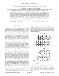
Figure 4. Sketch <strong>of</strong> the unit cell structures <strong>of</strong> ZB/3C, 4H, <strong>and</strong> WZ/2H.<br />
The theoretically obta<strong>in</strong>ed deformation <strong>of</strong> the unit cell as a whole <strong>and</strong><br />
the atomic basis with<strong>in</strong>, exaggerated by a factor <strong>of</strong> 30, is shown <strong>in</strong><br />
comparison to the ideal cell constructed from the cubic lattice constant<br />
(dashed l<strong>in</strong>es). The numerical values <strong>of</strong> the unit cell distortions,<br />
especially <strong>of</strong> the bond lengths d hex <strong>and</strong> d cub , are given for <strong>InSb</strong>.<br />
Qualitatively the same changes were found for <strong>InAs</strong>. The direction <strong>of</strong><br />
the displacement <strong>of</strong> the atoms due to the <strong>in</strong>ternal parameters is <strong>in</strong>dicated<br />
by arrows.<br />
The ZB reference values obta<strong>in</strong>ed by DFT calculations are a c =<br />
6.0321 Å for <strong>InAs</strong> <strong>and</strong> a c = 6.4542 Å for <strong>InSb</strong>. The absolute lattice<br />
parameters are <strong>in</strong>fluenced by the overb<strong>in</strong>d<strong>in</strong>g tendency due to the<br />
description <strong>of</strong> exchange <strong>and</strong> correlation with<strong>in</strong> the LDA. However,<br />
theerror<strong>in</strong>troducedbytheLDAisexpectedtobeverysimilarfor<br />
the ZB, 4H, <strong>and</strong> WZ structures, as these structures only differ by<br />
third next neighbor distances. Therefore, the underestimation <strong>of</strong> the<br />
lattice constants by less than 0.5% does not play a role s<strong>in</strong>ce only<br />
relative variations Δa <strong>and</strong> Δc, calculated us<strong>in</strong>g the reference values<br />
obta<strong>in</strong>ed by DFT, are compared with experimental f<strong>in</strong>d<strong>in</strong>gs.<br />
To determ<strong>in</strong>e the equilibrium lattice constants a <strong>and</strong> c, we<br />
calculated the total energy E on a regular (a,c) grid <strong>and</strong> <strong>in</strong>terpolated<br />
the E(a,c) surface with<strong>in</strong> a cubic <strong>in</strong>terpolation scheme. We <strong>in</strong>clude<br />
the IPs, i.e., the additional degrees <strong>of</strong> freedom for atomic relaxation,<br />
through a three-way optimization: In the first step we perform a<br />
E(a,c) <strong>in</strong>terpolation as described above with all IPs set to zero. In the<br />
second step we m<strong>in</strong>imize the energy with respect to the IPs, while<br />
the lattice parameters a <strong>and</strong> c are kept fixed. The last step is aga<strong>in</strong> a<br />
E(a,c) m<strong>in</strong>imization with the IPs <strong>of</strong> step two, <strong>in</strong> order to improve the<br />
accuracy for the description <strong>of</strong> the <strong>in</strong>terplay <strong>of</strong> lattice constants <strong>and</strong><br />
IPs. Compared to the most accurate multidimensional <strong>in</strong>terpolation,<br />
where all parameters (a,c <strong>and</strong> IPs) are optimized <strong>in</strong>dependently, the<br />
used three-step procedure scales better concern<strong>in</strong>g the number <strong>of</strong><br />
IPs <strong>and</strong> the grid size, thereby reduc<strong>in</strong>g the computational effort.<br />
Additionally, test calculations for WZ <strong>InAs</strong> show that the results <strong>of</strong><br />
different m<strong>in</strong>imization procedures are close to each other. The<br />
lattice constant a is almost the same, while c is slightly <strong>in</strong>creased by<br />
∼0.002 Å when us<strong>in</strong>g the multidimensional <strong>in</strong>terpolation scheme.<br />
Both XRD experiments <strong>and</strong> the DFT calculations show that<br />
deviations from the lattice constants obta<strong>in</strong>ed by simple geometrical<br />
conversion (eq 1) exist for both <strong>InAs</strong> <strong>and</strong> <strong>InSb</strong>, as shown <strong>in</strong> Table 2<br />
<strong>and</strong> Figure 3. The agreement between measurement <strong>and</strong> calculations<br />
is excellent. This holds not only for the sign <strong>and</strong> order <strong>of</strong> magnitude <strong>of</strong><br />
the lattice constant deviations Δa <strong>and</strong> Δc but also for the absolute<br />
values <strong>of</strong> these deviations. Figure 3 shows the perfect agreement for<br />
<strong>InAs</strong> polytypes, whereas slight deviations between theory <strong>and</strong><br />
experiment were found for <strong>InSb</strong>, which could be due to the rema<strong>in</strong><strong>in</strong>g<br />
effects <strong>of</strong> mutual stra<strong>in</strong><strong>in</strong>g <strong>of</strong> the different segments or the stronger<br />
overb<strong>in</strong>d<strong>in</strong>g tendency <strong>of</strong> the LDA functional used <strong>in</strong> the case <strong>of</strong> <strong>InSb</strong>.<br />
LETTER<br />
While the 4H segments are not expected to be stra<strong>in</strong> free, because <strong>of</strong><br />
their limited segment length <strong>of</strong> typically 5 15 nm, unexpectedly<br />
good agreement was found between theory <strong>and</strong> experiment. However,<br />
if a 4H segment is s<strong>and</strong>wiched between extended ZB <strong>and</strong> WZ<br />
segments,asisthecasehere(seeFigure1b),thestra<strong>in</strong><strong>in</strong>ducedby<br />
both sides could <strong>in</strong>deed compensate to zero. F<strong>in</strong>ite element model<strong>in</strong>g<br />
was used to determ<strong>in</strong>e the stra<strong>in</strong> state <strong>of</strong> such s<strong>and</strong>wiched 4H<br />
segments. For the simulations the theoretically obta<strong>in</strong>ed lattice<br />
parameters from Figure 3 <strong>and</strong> equal elastic properties <strong>of</strong> the<br />
hexagonal polytypes 45 were used. It was found that the stra<strong>in</strong> <strong>of</strong><br />
the 4H structure is antisymmetric along the segment, which can be<br />
understood because the WZ segment at the top <strong>and</strong> ZB segment at<br />
the bottom have approximately the opposite lattice mismatch with<br />
respect to 4H. The measured lattice parameter represents the average<br />
over the extent <strong>of</strong> the 4H segments, which is virtually equal to the<br />
relaxed value, as was confirmed by f<strong>in</strong>ite element calculations. This<br />
expla<strong>in</strong>s the agreement between theory <strong>and</strong> experiment even for the<br />
rather short segments. The experimental <strong>and</strong> theoretical relative<br />
aspect ratios (2c)/(pa) as given <strong>in</strong> Table 2 are almost the same, with a<br />
maximum deviation for 4H <strong>InSb</strong> <strong>of</strong> less than 0.1%. This agreement<br />
is astonish<strong>in</strong>g, because the DFT calculations treat ideal bulk polytypes<br />
<strong>in</strong> equilibrium at zero temperature, while XRD studies III Vbilayer<br />
stack<strong>in</strong>gs <strong>in</strong> nanowires with real structure, limited dimensions, <strong>and</strong><br />
<strong>in</strong>fluenced by growth k<strong>in</strong>etics. However, with<strong>in</strong> the experimental<br />
error no dependence <strong>of</strong> the lattice parameters on the wire diameter<br />
(samples C1 C3) could be found, <strong>in</strong>dicat<strong>in</strong>g that surface effects are<br />
negligible. Furthermore, no differences between the samples grown<br />
byMOVPE<strong>and</strong>CBEwerefound.<br />
Experiment <strong>and</strong> theory show that the occurrence <strong>of</strong> hexagonal<br />
bilayers tends to stretch the distances <strong>of</strong> atomic layers parallel to the<br />
c axis, while concomitantly the <strong>in</strong>-plane distances perpendicular to<br />
the c axis are reduced. The comb<strong>in</strong>ation <strong>of</strong> both effects results <strong>in</strong> the<br />
observed rise <strong>of</strong> the relative aspect ratio (2c)/(pa) with<strong>in</strong>creas<strong>in</strong>g<br />
hexagonality. Part <strong>of</strong> the aspect ratio change could be traced back to<br />
<strong>in</strong>ternal structure relaxation, i.e., the <strong>in</strong>fluence <strong>of</strong> <strong>in</strong>ternal parameters.<br />
Figure 4 shows sketches <strong>of</strong> the unit cells <strong>of</strong> the different polytypes,<br />
where the theoretically obta<strong>in</strong>ed deformation <strong>in</strong> comparison to the<br />
geometrically converted unit cell dimensions (dashed l<strong>in</strong>es) is<br />
<strong>in</strong>dicated. For both the WZ <strong>and</strong> 4H structure the bond length d hex<br />
<strong>of</strong> the hexagonal stacked bilayers is found to be stretched <strong>in</strong><br />
comparison to the correspond<strong>in</strong>g bond length <strong>in</strong> the ZB structure.<br />
The bond length <strong>in</strong>creases because <strong>of</strong> the repulsive force <strong>of</strong> the third<br />
next neighbors, which are located closer to each other <strong>in</strong> the case <strong>of</strong> a<br />
hexagonal stacked layer (see Figure 1c). In contrast to the general<br />
<strong>in</strong>crease <strong>of</strong> the unit cell dimension <strong>in</strong> the c direction, the bond length<br />
d cub <strong>of</strong> the cubic bilayers <strong>in</strong> 4H even decreases <strong>in</strong> comparison to ZB.<br />
The DFT calculations further show that the bond angles are also<br />
changed by some tenth <strong>of</strong> a degree, when the stack<strong>in</strong>g changes. The<br />
absolute values <strong>of</strong> the IPs ε, δ,<strong>and</strong>ε 0 are only <strong>of</strong> the order <strong>of</strong> 10 4<br />
<strong>and</strong> therefore similar to the case <strong>of</strong> SiC polytypes 21,46 <strong>and</strong> former<br />
calculations for GaAs WZ. 32,33 Nevertheless, the <strong>in</strong>ternal atomic<br />
relaxation considerably <strong>in</strong>fluences the results, i.e., a careful treatment<br />
<strong>of</strong> the cell IPs is important. For <strong>in</strong>stance, the mentioned <strong>in</strong>homogeneity<br />
<strong>of</strong> the bond lengths (d hex 6¼ d cub ) is directly connected to the<br />
IPs because d hex d cub =(|ε| þ |δ| þ |ε 0 |)c 4H holds for the 4H<br />
polytypes. Also the deviation <strong>of</strong> the characteristic bond length d hex is<br />
doubled via the displacements due to the IPs. The direction <strong>of</strong> the<br />
displacement <strong>of</strong> the atoms due to the <strong>in</strong>ternal parameters is<br />
<strong>in</strong>dicated by arrows <strong>in</strong> Figure 4. With decreas<strong>in</strong>g hexagonality, the<br />
<strong>in</strong>fluence <strong>of</strong> IPs becomes weaker.<br />
To determ<strong>in</strong>e the IPs directly from XRD experiments, absolute<br />
<strong>in</strong>tensity <strong>and</strong> shape <strong>of</strong> a complete set <strong>of</strong> Bragg peaks need to<br />
1487 dx.doi.org/10.1021/nl1041512 |Nano Lett. 2011, 11, 1483–1489
Nano Letters<br />
be determ<strong>in</strong>ed. 46,47 However, <strong>in</strong> the present case, the shape <strong>and</strong><br />
<strong>in</strong>tensity <strong>of</strong> the Bragg peaks from the NWs are <strong>in</strong>fluenced by<br />
ensemble averag<strong>in</strong>g effects, <strong>and</strong> only their positions can be evaluated<br />
with sufficiently high precision. An alternative technique which is <strong>in</strong><br />
pr<strong>in</strong>ciple able to determ<strong>in</strong>e the IPs experimentally would be<br />
extended X-ray absorption f<strong>in</strong>e structure (EXAFS) experiments,<br />
where the bond length <strong>of</strong> a certa<strong>in</strong> k<strong>in</strong>d <strong>of</strong> atoms is determ<strong>in</strong>ed.<br />
Although the required accuracy <strong>in</strong> the 10 3 Årangewasdemonstrated,<br />
e.g., <strong>in</strong> th<strong>in</strong> film experiments, 48 it is not possible to resolve<br />
them<strong>in</strong>utedifferences <strong>in</strong> the bond length <strong>of</strong> the tetrahedrally<br />
coord<strong>in</strong>ated atoms <strong>in</strong> NWs: The DFT calculations predict that<br />
each atom <strong>of</strong> a certa<strong>in</strong> k<strong>in</strong>d has various neighbors at slightly different<br />
distances, so that the obta<strong>in</strong>ed coord<strong>in</strong>ation shells would strongly<br />
overlap<strong>and</strong>cannotbeisolatedfromeachother.Thereforean<br />
experimental verification <strong>of</strong> the IPs is not directly possible <strong>in</strong> this<br />
case. However, about 20% <strong>of</strong> the calculated change <strong>in</strong> the lattice<br />
parameters a <strong>and</strong> c can be traced back to the <strong>in</strong>fluence <strong>of</strong> the IPs.<br />
These lattice parameters are measured with very high precision, so<br />
that the excellent agreement between experiment <strong>and</strong> theory (see<br />
Figure 3) <strong>in</strong>directly confirms the IP values.<br />
All geometric changes are clearly proportional to the hexagonality.<br />
In the case <strong>of</strong> 4H with hexagonality <strong>of</strong> 50%, they are less<br />
pronounced <strong>in</strong> comparison to WZ with 100% hexagonality. This is<br />
evident from Figure 4, where it is shown that each hexagonal stacked<br />
bilayer contributes to the stretch<strong>in</strong>g <strong>of</strong> the unit cell <strong>in</strong> the c axis,<br />
whereas it reduces the <strong>in</strong>-plane atomic distances: note that the<br />
absolute change <strong>of</strong> the unit cell size <strong>in</strong> the c direction is roughly the<br />
same for 4H <strong>and</strong> WZ, while the 4H unit cell conta<strong>in</strong>s twice as many<br />
layers as the WZ unit cell. The chemical trend is less significant. The<br />
relative c lattice constant variation Δc is enhanced with decreas<strong>in</strong>g<br />
bond ionicity from <strong>InAs</strong> to <strong>InSb</strong>, as shown <strong>in</strong> Figure 3, while an<br />
analogous tendency for Δa could not be observed.<br />
In conclusion, we employed X-ray diffraction to accurately<br />
determ<strong>in</strong>e the lattice parameters <strong>of</strong> <strong>InAs</strong> <strong>and</strong> <strong>InSb</strong> polytypes <strong>in</strong><br />
dependence <strong>of</strong> the hexagonality. Transmission electron microscopy<br />
was used to verify that extended segments <strong>of</strong> the ZB, WZ, <strong>and</strong> 4H<br />
phase are present <strong>and</strong> spatially separated. The results show excellent<br />
agreement with DFT calculations <strong>in</strong>clud<strong>in</strong>g the effect <strong>of</strong> <strong>in</strong>ternal<br />
parameters, which determ<strong>in</strong>e the distortion <strong>of</strong> the bond<strong>in</strong>g tetrahedra.<br />
Both experiments <strong>and</strong> theoretical results show that the lattice<br />
plane spac<strong>in</strong>g is altered when the structure changes from ZB to 4H<br />
<strong>and</strong> WZ <strong>and</strong> that the simple geometric conversion formulas are not<br />
applicable. For the 4H <strong>and</strong> WZ polytypes <strong>of</strong> <strong>InAs</strong> <strong>and</strong> <strong>InSb</strong>, we<br />
observe an <strong>in</strong>crease <strong>of</strong> the (000.1) lattice plane spac<strong>in</strong>g <strong>in</strong> the c<br />
direction by approximately 0.2 0.25% <strong>and</strong> 0.4 0.5%, respectively.<br />
The variation <strong>of</strong> the <strong>in</strong>-plane lattice constant shows the <strong>in</strong>verse<br />
behavior <strong>and</strong> was found to be decreased by approximately 0.12%<br />
<strong>and</strong> 0.25% for the 4H <strong>and</strong> WZ structures. These accurate structural<br />
data enable precise calculations <strong>of</strong> the b<strong>and</strong> structure <strong>and</strong> b<strong>and</strong><br />
alignment <strong>of</strong> the hexagonal polytypes. This will be essential to<br />
underst<strong>and</strong> the electronic <strong>and</strong> optical properties <strong>of</strong> advanced pure<br />
crystal phase <strong>and</strong> polytypic III V nanowire devices.<br />
’ ASSOCIATED CONTENT<br />
b S Support<strong>in</strong>g Information. Animation <strong>of</strong> the unit cell<br />
structures <strong>of</strong> ZB/3C, 4H, <strong>and</strong> WZ/2H as well as their deformations,<br />
show<strong>in</strong>g (exaggerated by a factor <strong>of</strong> 30) the deviations <strong>of</strong><br />
the structure obta<strong>in</strong>ed by geometric conversion, similar to what is<br />
shown <strong>in</strong> Figure 4. This material is available free <strong>of</strong> charge via the<br />
Internet at http://pubs.acs.org.<br />
’ AUTHOR INFORMATION<br />
LETTER<br />
Correspond<strong>in</strong>g Author<br />
*E-mail: dom<strong>in</strong>ik.kriegner@jku.at; christian.panse@uni-jena.de.<br />
’ ACKNOWLEDGMENT<br />
The authors thank the staff at BW2 Hasylab (D. Novikov) for<br />
assistance with the beaml<strong>in</strong>e setup <strong>and</strong> E. Vorhauer <strong>and</strong> F. B<strong>in</strong>der<br />
for technical assistance with the laboratory setups. We acknowledge<br />
the f<strong>in</strong>ancial support from FWF Vienna (SFB025 IR-ON)<br />
<strong>and</strong> the EC (AMON-Ra, 214814, ELISA, 226716 <strong>and</strong> ETSF,<br />
211956). Part <strong>of</strong> this work was supported by the Nanometer<br />
<strong>Structure</strong> Consortium at Lund University (nmC@LU), the<br />
Swedish Foundation for Strategic Research (SSF), the Swedish<br />
Research Council (VR), <strong>and</strong> the Knut <strong>and</strong> Alice Wallenberg<br />
Foundation. We gratefully acknowledge the use <strong>of</strong> the TEM<br />
facilities at the Center for Electron Nanoscopy at the Technical<br />
University <strong>of</strong> Denmark.<br />
’ REFERENCES<br />
(1) Thel<strong>and</strong>er, C.; Agarwal, P.; Brongersma, S.; Eymery, J.; Fe<strong>in</strong>er,<br />
L.; Forchel, A.; Scheffler, M.; Riess, W.; Ohlsson, B.; G€osele, U.;<br />
Samuelson, L. Mater. Today 2006, 9, 28–35.<br />
(2) Lieber, C. M.; Wang, Z. L. MRS Bull. 2007, 32, 99.<br />
(3) Kitauchi, Y.; Kobayashi, Y.; Tomioka, K.; Hara, S.; Hiruma, K.;<br />
Fukui, T.; Motohisa, J. Nano Lett. 2010, 10, 1699–1703.<br />
(4) Spirkoska, D.; et al. Phys. Rev. B 2009, 80, No. 245325.<br />
(5) Dheeraj, D. L.; Patriarche, G.; Zhou, H.; Hoang, T. B.; Moses,<br />
A. F.; Grønsberg, S.; van Helvoort, A. T. J.; Fiml<strong>and</strong>, B.; Weman, H.<br />
Nano Lett. 2008, 8, 4459–4463.<br />
(6) Car<strong>of</strong>f, P.; Dick, K. A.; Johansson, J.; Mess<strong>in</strong>g, M. E.; Deppert, K.;<br />
Samuelson, L. Nat. Nanotechnol. 2009, 4, 50–55.<br />
(7) Dick, K. A.; Thel<strong>and</strong>er, C.; Samuelson, L.; Car<strong>of</strong>f, P.Nano Lett.<br />
2010, 10, 3494–3499.<br />
(8) M<strong>and</strong>l, B.; Dick, K. A.; Kriegner, D.; Kepl<strong>in</strong>ger, M.; Bauer, G.;<br />
Stangl, J.; Deppert, K. Nanotechnol. 2011, 22, 145603.<br />
(9) Algra, R. E.; Verheijen, M. A.; Borgstrom, M. T.; Fe<strong>in</strong>er, L.-F.;<br />
Imm<strong>in</strong>k, G.; van Enckevort, W. J. P.; Vlieg, E.; Bakkers, E. P. A. M. Nature<br />
2008, 456, 369–372.<br />
(10) Soshnikov, I.; Cirl<strong>in</strong>, G.; Sibirev, N.; Dubrovskii, V.; Samsonenko,<br />
Y.;Litv<strong>in</strong>ov,D.;Gerthsen,D.Tech. Phys. Lett. 2008, 34, 538–541.<br />
(11) Joyce, H. J.; Wong-Leung, J.; Gao, Q.; Tan, H. H.; Jagadish, C.<br />
Nano Lett. 2010, 10, 908–915.<br />
(12) Krogstrup, P.; Popovitz-Biro, R.; Johnson, E.; Madsen, M. H.;<br />
Nyg ard, J.; Shtrikman, H. Nano Lett. 2010, 10, 4475–4482.<br />
(13) Shtrikman, H.; Popovitz-Biro, R.; Kret<strong>in</strong><strong>in</strong>, A.; Heiblum, M.<br />
Nano Lett. 2009, 9, 215–219.<br />
(14) Shtrikman, H.; Popovitz-Biro, R.; Kret<strong>in</strong><strong>in</strong>, A.; Houben, L.;<br />
Heiblum, M.; Bukaza, M.; Galicka, M.; Buczko, R.; Kacman, P. Nano Lett.<br />
2009, 9, 1506–1510.<br />
(15) Zhang, L.; Luo, J.-W.; Zunger, A.; Akopian, N.; Zwiller, V.;<br />
Harm<strong>and</strong>, J.-C. Nano Lett. 2010, 10, 4055–4060.<br />
(16) Akiyama, T.; Yamashita, T.; Nakamura, K.; Ito, T. Nano Lett.<br />
2010, 10, 4614–4618.<br />
(17) Tr€ag ardh, J.; Persson, A. I.; Wagner, J. B.; Hessman, D.;<br />
Samuelson, L. J. Appl. Phys. 2007, 101, No. 123701.<br />
(18) Zardo, I.; Conesa-Boj, S.; Peiro, F.; Morante, J. R.; Arbiol, J.;<br />
Uccelli, E.; Abstreiter, G.; Fontcuberta i Morral, A. Phys. Rev. B 2009,<br />
80, No. 245324.<br />
(19) Akopian, N.; Patriarche, G.; Liu, L.; Harm<strong>and</strong>, J.-C.; Zwiller, V.<br />
Nano Lett. 2010, 10, 1198–1201.<br />
(20) Pemasiri, K.; Montazeri, M.; Gass, R.; Smith, L. M.; Jackson,<br />
H. E.; Yarrison-Rice, J.; Paiman, S.; Gao, Q.; Tan, H. H.; Jagadish, C.;<br />
Zhang, X.; Zou, J. Nano Lett. 2009, 9, 648–654.<br />
1488 dx.doi.org/10.1021/nl1041512 |Nano Lett. 2011, 11, 1483–1489
Nano Letters<br />
LETTER<br />
(21) K€ackell, P.; Wenzien, B.; Bechstedt, F. Phys. Rev. B 1994,<br />
50, 17037–17046.<br />
(22) Takahashi, K.; Morizumi, T. Jpn. J. Appl. Phys. 1966, 5,<br />
657–662.<br />
(23) M<strong>and</strong>l, B.; Stangl, J.; M artensson, T.; Mikkelsen, A.; Eriksson,<br />
J.; Karlsson, L. S.; Bauer, G.; Samuelson, L.; Seifert, W. Nano Lett. 2006,<br />
6, 1817–1821.<br />
(24) Bauer, J.; Pietsch, U.; Davydok, A.; Biermanns, A.; Grenzer, J.;<br />
Gottschalch, V.; Wagner, G. Appl. Phys. A: Mater. Sci. Process. 2009,<br />
96, 851–859.<br />
(25) Mariager, S. O.; Lauridsen, S. L.; Dohn, A.; Bovet, N.; Sørensen,<br />
C. B.; Schlepuetz, C. M.; Willmott, P. R.; Feidenhans’l, R. J. Appl.<br />
<strong>Crystal</strong>logr. 2009, 42, 369–375.<br />
(26) We use Miller <strong>in</strong>dices (hkl) <strong>and</strong> Bravais <strong>in</strong>dices <strong>and</strong> (hki.l) with<br />
i = h k to denote hexagonal structures.<br />
(27) Zanolli, Z.; Fuchs, F.; Furthm€uller, J.; von Barth, U.; Bechstedt,<br />
F. Phys. Rev. B 2007, 75, No. 245121.<br />
(28) De, A.; Pryor, C. E. Phys. Rev. B 2010, 81, No. 155210.<br />
(29) Feynman, R. P. Phys. Rev. 1939, 56, 340–343.<br />
(30) Lawaetz, P. Phys. Rev. B 1972, 5, 4039–4045.<br />
(31) McMahon, M. I.; Nelmes, R. J. Phys. Rev. Lett. 2005, 95, No.<br />
215505.<br />
(32) Yeh, C.-Y.; Lu, Z. W.; Froyen, S.; Zunger, A. Phys. Rev. B 1992,<br />
46, 10086–10097.<br />
(33) Mujica, A.; Needs, R. J.; Mu~noz, A. Phys. Rev. B 1995,<br />
52, 8881–8892.<br />
(34) Ercolani, D.; Rossi, F.; Li, A.; Roddaro, S.; Grillo, V.; Salviati, G.;<br />
Beltram, F.; Sorba, L. Nanotechnology 2009, 20, No. 505605.<br />
(35) Fr€oberg, L. E.; Seifert, W.; Johansson, J. Phys. Rev. B 2007,<br />
76, No. 153401.<br />
(36) M<strong>and</strong>l, B.; Stangl, J.; Hilner, E.; Zakharov, A. A.; Hillerich, K.;<br />
Dey, A. W.; Samuelson, L.; Bauer, G.; Deppert, K.; Mikkelsen, A. Nano<br />
Lett. 2010, 10, 4443–4449.<br />
(37) Madelung, O. Semiconductors: data h<strong>and</strong>book; Spr<strong>in</strong>ger: Berl<strong>in</strong>,<br />
2004.<br />
(38) Kresse, G.; Furthm€uller, J. Comput. Mater. Sci. 1996, 6, 15–50.<br />
(39) Hobbs, D.; Kresse, G.; Hafner, J. Phys. Rev. B 2000,<br />
62, 11556–11570.<br />
(40) Kresse, G.; Joubert, D. Phys. Rev. B 1999, 59, 1758–1775.<br />
(41) Kim, Y.-S.; Hummer, K.; Kresse, G. Phys. Rev. B 2009, 80, No.<br />
035203.<br />
(42) Haas, P.; Tran, F.; Blaha, P. Phys. Rev. B 2009, 79, No. 085104.<br />
(43) Wyckh<strong>of</strong>f, R.<strong>Crystal</strong> <strong>Structure</strong>s; Interscience Publishers: New<br />
York, 1964; Vol. 1.<br />
(44) This approach led to to good agreement with available experimental<br />
data for SiC polytypes, as is shown <strong>in</strong> ref 21.<br />
(45) Mart<strong>in</strong>, R. M. Phys. Rev. B 1972, 6, 4546–4553.<br />
(46) Bauer, A.; Kr€ausslich, J.; Dressler, L.; Kuschnerus, P.; Wolf, J.;<br />
Goetz, K.; K€ackell, P.; Furthm€uller, J.; Bechstedt, F. Phys. Rev. B 1998,<br />
57, 2647–2650.<br />
(47) Bechstedt, F.; K€ackell, P.; Zywietz, A.; Karch, K.; Adolph, B.;<br />
Tenelsen, K.; Furthm€uller, J. Phys. Status Solidi B 1997, 202, 35–62.<br />
(48) Kuwahara, Y.; Oyanagi, H.; Shioda, R.; Takeda, Y.; Yamaguchi,<br />
H.; Aono, M. Jpn. J. Appl. Phys. 1994, 33, 5631.<br />
1489 dx.doi.org/10.1021/nl1041512 |Nano Lett. 2011, 11, 1483–1489