Unit Cell Structure of Crystal Polytypes in InAs and InSb Nanowires
Unit Cell Structure of Crystal Polytypes in InAs and InSb Nanowires
Unit Cell Structure of Crystal Polytypes in InAs and InSb Nanowires

You also want an ePaper? Increase the reach of your titles
YUMPU automatically turns print PDFs into web optimized ePapers that Google loves.
Nano Letters<br />
be determ<strong>in</strong>ed. 46,47 However, <strong>in</strong> the present case, the shape <strong>and</strong><br />
<strong>in</strong>tensity <strong>of</strong> the Bragg peaks from the NWs are <strong>in</strong>fluenced by<br />
ensemble averag<strong>in</strong>g effects, <strong>and</strong> only their positions can be evaluated<br />
with sufficiently high precision. An alternative technique which is <strong>in</strong><br />
pr<strong>in</strong>ciple able to determ<strong>in</strong>e the IPs experimentally would be<br />
extended X-ray absorption f<strong>in</strong>e structure (EXAFS) experiments,<br />
where the bond length <strong>of</strong> a certa<strong>in</strong> k<strong>in</strong>d <strong>of</strong> atoms is determ<strong>in</strong>ed.<br />
Although the required accuracy <strong>in</strong> the 10 3 Årangewasdemonstrated,<br />
e.g., <strong>in</strong> th<strong>in</strong> film experiments, 48 it is not possible to resolve<br />
them<strong>in</strong>utedifferences <strong>in</strong> the bond length <strong>of</strong> the tetrahedrally<br />
coord<strong>in</strong>ated atoms <strong>in</strong> NWs: The DFT calculations predict that<br />
each atom <strong>of</strong> a certa<strong>in</strong> k<strong>in</strong>d has various neighbors at slightly different<br />
distances, so that the obta<strong>in</strong>ed coord<strong>in</strong>ation shells would strongly<br />
overlap<strong>and</strong>cannotbeisolatedfromeachother.Thereforean<br />
experimental verification <strong>of</strong> the IPs is not directly possible <strong>in</strong> this<br />
case. However, about 20% <strong>of</strong> the calculated change <strong>in</strong> the lattice<br />
parameters a <strong>and</strong> c can be traced back to the <strong>in</strong>fluence <strong>of</strong> the IPs.<br />
These lattice parameters are measured with very high precision, so<br />
that the excellent agreement between experiment <strong>and</strong> theory (see<br />
Figure 3) <strong>in</strong>directly confirms the IP values.<br />
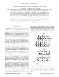
All geometric changes are clearly proportional to the hexagonality.<br />
In the case <strong>of</strong> 4H with hexagonality <strong>of</strong> 50%, they are less<br />
pronounced <strong>in</strong> comparison to WZ with 100% hexagonality. This is<br />
evident from Figure 4, where it is shown that each hexagonal stacked<br />
bilayer contributes to the stretch<strong>in</strong>g <strong>of</strong> the unit cell <strong>in</strong> the c axis,<br />
whereas it reduces the <strong>in</strong>-plane atomic distances: note that the<br />
absolute change <strong>of</strong> the unit cell size <strong>in</strong> the c direction is roughly the<br />
same for 4H <strong>and</strong> WZ, while the 4H unit cell conta<strong>in</strong>s twice as many<br />
layers as the WZ unit cell. The chemical trend is less significant. The<br />
relative c lattice constant variation Δc is enhanced with decreas<strong>in</strong>g<br />
bond ionicity from <strong>InAs</strong> to <strong>InSb</strong>, as shown <strong>in</strong> Figure 3, while an<br />
analogous tendency for Δa could not be observed.<br />
In conclusion, we employed X-ray diffraction to accurately<br />
determ<strong>in</strong>e the lattice parameters <strong>of</strong> <strong>InAs</strong> <strong>and</strong> <strong>InSb</strong> polytypes <strong>in</strong><br />
dependence <strong>of</strong> the hexagonality. Transmission electron microscopy<br />
was used to verify that extended segments <strong>of</strong> the ZB, WZ, <strong>and</strong> 4H<br />
phase are present <strong>and</strong> spatially separated. The results show excellent<br />
agreement with DFT calculations <strong>in</strong>clud<strong>in</strong>g the effect <strong>of</strong> <strong>in</strong>ternal<br />
parameters, which determ<strong>in</strong>e the distortion <strong>of</strong> the bond<strong>in</strong>g tetrahedra.<br />
Both experiments <strong>and</strong> theoretical results show that the lattice<br />
plane spac<strong>in</strong>g is altered when the structure changes from ZB to 4H<br />
<strong>and</strong> WZ <strong>and</strong> that the simple geometric conversion formulas are not<br />
applicable. For the 4H <strong>and</strong> WZ polytypes <strong>of</strong> <strong>InAs</strong> <strong>and</strong> <strong>InSb</strong>, we<br />
observe an <strong>in</strong>crease <strong>of</strong> the (000.1) lattice plane spac<strong>in</strong>g <strong>in</strong> the c<br />
direction by approximately 0.2 0.25% <strong>and</strong> 0.4 0.5%, respectively.<br />
The variation <strong>of</strong> the <strong>in</strong>-plane lattice constant shows the <strong>in</strong>verse<br />
behavior <strong>and</strong> was found to be decreased by approximately 0.12%<br />
<strong>and</strong> 0.25% for the 4H <strong>and</strong> WZ structures. These accurate structural<br />
data enable precise calculations <strong>of</strong> the b<strong>and</strong> structure <strong>and</strong> b<strong>and</strong><br />
alignment <strong>of</strong> the hexagonal polytypes. This will be essential to<br />
underst<strong>and</strong> the electronic <strong>and</strong> optical properties <strong>of</strong> advanced pure<br />
crystal phase <strong>and</strong> polytypic III V nanowire devices.<br />
’ ASSOCIATED CONTENT<br />
b S Support<strong>in</strong>g Information. Animation <strong>of</strong> the unit cell<br />
structures <strong>of</strong> ZB/3C, 4H, <strong>and</strong> WZ/2H as well as their deformations,<br />
show<strong>in</strong>g (exaggerated by a factor <strong>of</strong> 30) the deviations <strong>of</strong><br />
the structure obta<strong>in</strong>ed by geometric conversion, similar to what is<br />
shown <strong>in</strong> Figure 4. This material is available free <strong>of</strong> charge via the<br />
Internet at http://pubs.acs.org.<br />
’ AUTHOR INFORMATION<br />
LETTER<br />
Correspond<strong>in</strong>g Author<br />
*E-mail: dom<strong>in</strong>ik.kriegner@jku.at; christian.panse@uni-jena.de.<br />
’ ACKNOWLEDGMENT<br />
The authors thank the staff at BW2 Hasylab (D. Novikov) for<br />
assistance with the beaml<strong>in</strong>e setup <strong>and</strong> E. Vorhauer <strong>and</strong> F. B<strong>in</strong>der<br />
for technical assistance with the laboratory setups. We acknowledge<br />
the f<strong>in</strong>ancial support from FWF Vienna (SFB025 IR-ON)<br />
<strong>and</strong> the EC (AMON-Ra, 214814, ELISA, 226716 <strong>and</strong> ETSF,<br />
211956). Part <strong>of</strong> this work was supported by the Nanometer<br />
<strong>Structure</strong> Consortium at Lund University (nmC@LU), the<br />
Swedish Foundation for Strategic Research (SSF), the Swedish<br />
Research Council (VR), <strong>and</strong> the Knut <strong>and</strong> Alice Wallenberg<br />
Foundation. We gratefully acknowledge the use <strong>of</strong> the TEM<br />
facilities at the Center for Electron Nanoscopy at the Technical<br />
University <strong>of</strong> Denmark.<br />
’ REFERENCES<br />
(1) Thel<strong>and</strong>er, C.; Agarwal, P.; Brongersma, S.; Eymery, J.; Fe<strong>in</strong>er,<br />
L.; Forchel, A.; Scheffler, M.; Riess, W.; Ohlsson, B.; G€osele, U.;<br />
Samuelson, L. Mater. Today 2006, 9, 28–35.<br />
(2) Lieber, C. M.; Wang, Z. L. MRS Bull. 2007, 32, 99.<br />
(3) Kitauchi, Y.; Kobayashi, Y.; Tomioka, K.; Hara, S.; Hiruma, K.;<br />
Fukui, T.; Motohisa, J. Nano Lett. 2010, 10, 1699–1703.<br />
(4) Spirkoska, D.; et al. Phys. Rev. B 2009, 80, No. 245325.<br />
(5) Dheeraj, D. L.; Patriarche, G.; Zhou, H.; Hoang, T. B.; Moses,<br />
A. F.; Grønsberg, S.; van Helvoort, A. T. J.; Fiml<strong>and</strong>, B.; Weman, H.<br />
Nano Lett. 2008, 8, 4459–4463.<br />
(6) Car<strong>of</strong>f, P.; Dick, K. A.; Johansson, J.; Mess<strong>in</strong>g, M. E.; Deppert, K.;<br />
Samuelson, L. Nat. Nanotechnol. 2009, 4, 50–55.<br />
(7) Dick, K. A.; Thel<strong>and</strong>er, C.; Samuelson, L.; Car<strong>of</strong>f, P.Nano Lett.<br />
2010, 10, 3494–3499.<br />
(8) M<strong>and</strong>l, B.; Dick, K. A.; Kriegner, D.; Kepl<strong>in</strong>ger, M.; Bauer, G.;<br />
Stangl, J.; Deppert, K. Nanotechnol. 2011, 22, 145603.<br />
(9) Algra, R. E.; Verheijen, M. A.; Borgstrom, M. T.; Fe<strong>in</strong>er, L.-F.;<br />
Imm<strong>in</strong>k, G.; van Enckevort, W. J. P.; Vlieg, E.; Bakkers, E. P. A. M. Nature<br />
2008, 456, 369–372.<br />
(10) Soshnikov, I.; Cirl<strong>in</strong>, G.; Sibirev, N.; Dubrovskii, V.; Samsonenko,<br />
Y.;Litv<strong>in</strong>ov,D.;Gerthsen,D.Tech. Phys. Lett. 2008, 34, 538–541.<br />
(11) Joyce, H. J.; Wong-Leung, J.; Gao, Q.; Tan, H. H.; Jagadish, C.<br />
Nano Lett. 2010, 10, 908–915.<br />
(12) Krogstrup, P.; Popovitz-Biro, R.; Johnson, E.; Madsen, M. H.;<br />
Nyg ard, J.; Shtrikman, H. Nano Lett. 2010, 10, 4475–4482.<br />
(13) Shtrikman, H.; Popovitz-Biro, R.; Kret<strong>in</strong><strong>in</strong>, A.; Heiblum, M.<br />
Nano Lett. 2009, 9, 215–219.<br />
(14) Shtrikman, H.; Popovitz-Biro, R.; Kret<strong>in</strong><strong>in</strong>, A.; Houben, L.;<br />
Heiblum, M.; Bukaza, M.; Galicka, M.; Buczko, R.; Kacman, P. Nano Lett.<br />
2009, 9, 1506–1510.<br />
(15) Zhang, L.; Luo, J.-W.; Zunger, A.; Akopian, N.; Zwiller, V.;<br />
Harm<strong>and</strong>, J.-C. Nano Lett. 2010, 10, 4055–4060.<br />
(16) Akiyama, T.; Yamashita, T.; Nakamura, K.; Ito, T. Nano Lett.<br />
2010, 10, 4614–4618.<br />
(17) Tr€ag ardh, J.; Persson, A. I.; Wagner, J. B.; Hessman, D.;<br />
Samuelson, L. J. Appl. Phys. 2007, 101, No. 123701.<br />
(18) Zardo, I.; Conesa-Boj, S.; Peiro, F.; Morante, J. R.; Arbiol, J.;<br />
Uccelli, E.; Abstreiter, G.; Fontcuberta i Morral, A. Phys. Rev. B 2009,<br />
80, No. 245324.<br />
(19) Akopian, N.; Patriarche, G.; Liu, L.; Harm<strong>and</strong>, J.-C.; Zwiller, V.<br />
Nano Lett. 2010, 10, 1198–1201.<br />
(20) Pemasiri, K.; Montazeri, M.; Gass, R.; Smith, L. M.; Jackson,<br />
H. E.; Yarrison-Rice, J.; Paiman, S.; Gao, Q.; Tan, H. H.; Jagadish, C.;<br />
Zhang, X.; Zou, J. Nano Lett. 2009, 9, 648–654.<br />
1488 dx.doi.org/10.1021/nl1041512 |Nano Lett. 2011, 11, 1483–1489