Unit Cell Structure of Crystal Polytypes in InAs and InSb Nanowires
Unit Cell Structure of Crystal Polytypes in InAs and InSb Nanowires
Unit Cell Structure of Crystal Polytypes in InAs and InSb Nanowires

Create successful ePaper yourself
Turn your PDF publications into a flip-book with our unique Google optimized e-Paper software.
Nano Letters<br />
LETTER<br />
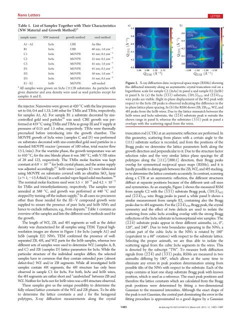
Table 1. List <strong>of</strong> Samples Together with Their Characteristics<br />
(NW Material <strong>and</strong> Growth Method) a<br />
sample name NW material growth method seed method<br />
A1 A2 <strong>InAs</strong> CBE Au film<br />
B1 <strong>InAs</strong> CBE 60 nm; 1.0 μm 2<br />
C1 <strong>InAs</strong> MOVPE 45 nm; 0.5 μm 2<br />
C2 <strong>InAs</strong> MOVPE 25 nm; 0.5 μm 2<br />
C3 <strong>InAs</strong> MOVPE 45 nm; 1.0 μm 2<br />
D1 <strong>InAs</strong> MOVPE 45 nm; 0.5 μm 2<br />
D2 <strong>InAs</strong> MOVPE 50 nm; 1.0 μm 2<br />
D3 <strong>InAs</strong> MOVPE 55 nm; 0.5 μm 2<br />
E1 E2 <strong>InSb</strong> MOVPE self-seeded<br />
a All samples were grown on <strong>InAs</strong> (111)B substrates. Au particles with<br />
given diameter <strong>and</strong> area density were used as seed particles except for<br />
samples A <strong>and</strong> E.<br />
the <strong>in</strong>jector. <strong>Nanowires</strong> were grown at 420 °C with the l<strong>in</strong>e pressures<br />
set to 0.6, 0.4 <strong>and</strong> 1.33, 2.66 mbar for TMIn <strong>and</strong> TBAs, respectively,<br />
for samples A1, A2. For sample B1 a substrate decorated by sizecontrolled<br />
gold seed particles 35 was used: CBE growth was performed<br />
at 419 °C us<strong>in</strong>g TMIn <strong>and</strong> TBAs as group III <strong>and</strong> V supply at<br />
pressures <strong>of</strong> 0.15 <strong>and</strong> 1.5 mbar, respectively. TBAs were thermally<br />
precracked before <strong>in</strong>troduc<strong>in</strong>g <strong>in</strong>to the growth chamber. The<br />
MOVPE growth <strong>of</strong> <strong>InAs</strong> wires (samples C <strong>and</strong> D) was performed<br />
on substrates decorated with size-controlled gold seed particles <strong>in</strong> a<br />
st<strong>and</strong>ard MOVPE reactor (pressure <strong>of</strong> 100 mbar, total reactor flow<br />
13 L/m<strong>in</strong>). For the wurtzite phase, the growth temperature was set<br />
to 410 °C, for the z<strong>in</strong>c blende phase it was 380 °C, with V/III ratios<br />
<strong>of</strong> 28 <strong>and</strong> 123, respectively. The TMIn molar fraction was kept<br />
constant at 6.9 10 6 for both crystal phases, <strong>and</strong> the ars<strong>in</strong>e supply<br />
was adjusted accord<strong>in</strong>gly. 6,7 <strong>InSb</strong> wires (samples E) were fabricated<br />
us<strong>in</strong>g MOVPE on substrates covered with an ultrath<strong>in</strong> SiO x layer<br />
(x ≈ 1, ∼13 Å thick) <strong>in</strong> a self-seeded vapor liquid solid mechanism. 36<br />
The nom<strong>in</strong>al molar fractions used were 5.5 10 6 <strong>and</strong> 4.2 10 5<br />
for TMIn <strong>and</strong> trimethylantimony, respectively. The samples were<br />
annealed at 580 °C,<strong>and</strong>growthwasperformedat440°C <strong>and</strong><br />
stopped by turn<strong>in</strong>g <strong>of</strong>f the <strong>in</strong>dium supply. 8 In all cases no precursors<br />
other than those needed for the III V compound growth were<br />
supplied to ensure the presence <strong>of</strong> pure <strong>InAs</strong> <strong>and</strong> <strong>InSb</strong> NWs <strong>and</strong><br />
hence to exclude <strong>in</strong>fluences, e.g., from dopants. 9 Table 1 conta<strong>in</strong>s an<br />
overview <strong>of</strong> the samples <strong>and</strong> lists the different seed methods used for<br />
the growth.<br />
Thelength<strong>of</strong>WZ,ZB,<strong>and</strong>4Hsegmentsaswellasthedefect<br />
density was characterized for all samples us<strong>in</strong>g TEM. Typical highresolution<br />
images are shown <strong>in</strong> Figure 1 for <strong>InAs</strong> (sample A1) <strong>and</strong><br />
<strong>InSb</strong> (sample E2) NWs. TEM confirmed the presence <strong>of</strong> wellseparated<br />
ZB, 4H, <strong>and</strong> WZ parts for the <strong>InSb</strong> samples, whereas two<br />
different sets <strong>of</strong> samples were used to determ<strong>in</strong>e WZ (samples A, B,<br />
<strong>and</strong> C) <strong>and</strong> ZB (samples D) lattice parameters for <strong>InAs</strong>. While the<br />
particular structure <strong>of</strong> the <strong>in</strong>dividual samples differs, the selected<br />
samples have <strong>in</strong> common that they conta<strong>in</strong> extended pure (almost<br />
defect-free) WZ <strong>and</strong>/or ZB segments. While all <strong>in</strong>vestigated <strong>InSb</strong><br />
samples conta<strong>in</strong> 4H segments, the 4H structure has only been<br />
observed <strong>in</strong> sample C1 for <strong>InAs</strong>. For both, <strong>InAs</strong> <strong>and</strong> <strong>InSb</strong> wires,<br />
the 4H segments are rather short <strong>and</strong> “s<strong>and</strong>wiched” between ZB <strong>and</strong><br />
WZ. Neither for <strong>InAs</strong> nor for <strong>InSb</strong> wires was a 6H structure observed.<br />
These samples give us the unique possibility to determ<strong>in</strong>e the<br />
fully relaxed lattice constants <strong>of</strong> the WZ <strong>and</strong> ZB phases. To be able<br />
to determ<strong>in</strong>e the lattice constants a <strong>and</strong> c for the hexagonal<br />
polytypes, X-ray diffraction measurements along the crystal<br />
Figure 2. X-ray diffraction data: reciprocal space maps (RSMs) show<strong>in</strong>g<br />
the diffracted <strong>in</strong>tensity along an asymmetric crystal truncation rod on a<br />
logarithmic scale for sample C2 (<strong>InAs</strong>) <strong>in</strong> panel a <strong>and</strong> sample E2 (<strong>InSb</strong>)<br />
<strong>in</strong> panel b. In (a) the <strong>InAs</strong> (331) substrate, (101.5) WZ , <strong>and</strong> (224) TW<br />
wire peaks are visible. Slight <strong>in</strong>-plane displacement <strong>of</strong> the WZ peak with<br />
respect to the <strong>InAs</strong> ZB peaks is observed <strong>in</strong>dicat<strong>in</strong>g the difference <strong>in</strong> the<br />
<strong>in</strong>-plane lattice plane spac<strong>in</strong>g. In (b) the RSM shows ZB, ZB TW , WZ, <strong>and</strong><br />
4H peaks from the <strong>InSb</strong> wires. Due to the lattice mismatch between the<br />
<strong>InSb</strong> wires <strong>and</strong> <strong>InAs</strong> substrate, the (224) substrate peak is outside the<br />
shown range <strong>in</strong> panel b, whereas the substrates (331) peak <strong>in</strong> panel a<br />
overlaps with the scatter<strong>in</strong>g signal from the wires.<br />
truncationrod(CTR)atanasymmetricreflection are performed. In<br />
this geometry, scatter<strong>in</strong>g from planes with a certa<strong>in</strong> angle to the<br />
(111) substrate surface is recorded, <strong>and</strong> from the positions <strong>of</strong> the<br />
Bragg peaks we determ<strong>in</strong>e the lattice parameters both along the<br />
growth direction <strong>and</strong> perpendicular to it. Due to the structure factor<br />
selection rules <strong>and</strong> the very similar lattice plane spac<strong>in</strong>gs for all<br />
polytypes along the [111]/[000.1] direction, their Bragg peaks<br />
overlap for symmetrical reciprocal space maps (RSMs), <strong>and</strong> it is<br />
hardly possible to dist<strong>in</strong>guish between the ZB, WZ, <strong>and</strong> 4H stack<strong>in</strong>g,<br />
or to determ<strong>in</strong>e the lattice constants accurately. In contrast, scann<strong>in</strong>g<br />
alongaCTRatanasymmetricreflection, the different structures<br />
diffract at separate positions because <strong>of</strong> the different unit cell sizes<br />
<strong>and</strong> symmetries. As an example, Figure 2 shows the measured RSM<br />
from sample C2 with the (331) substrate Bragg peak, (101.5) WZ<br />
<strong>and</strong> (224) TW wire Bragg peaks <strong>in</strong> panel a, while panel b shows a<br />
similar measurement from sample E2, conta<strong>in</strong><strong>in</strong>g also the Bragg<br />
peaks due to 4H segments. For the (224) TW Bragg peak, the crystal<br />
symmetry <strong>and</strong> the effect <strong>of</strong> tw<strong>in</strong> defects are used to isolate the<br />
scatter<strong>in</strong>g from cubic <strong>InAs</strong> avoid<strong>in</strong>g overlap with the strong Bragg<br />
reflections <strong>of</strong> the <strong>InAs</strong> substrate <strong>in</strong> homoepitaxial wire samples: The<br />
(224) substrate peaks appear <strong>in</strong> three different azimuths, i.e., 0°,<br />
120°, <strong>and</strong> 240°. Due to tw<strong>in</strong> boundaries appear<strong>in</strong>g <strong>in</strong> the NWs, a<br />
certa<strong>in</strong> part <strong>of</strong> the cubic <strong>InAs</strong> <strong>in</strong> the NWs is rotated by 180°<br />
(equivalent to a 60° rotation) with respect to the substrate lattice.<br />
Select<strong>in</strong>g the proper azimuth, we are thus able to isolate the<br />
scatter<strong>in</strong>g signal from the cubic <strong>InAs</strong> segments <strong>in</strong> the wires. This<br />
is denoted by the subscript “TW”. Tomeasurebothdiffraction<br />
signals from (224) <strong>and</strong> (331) peaks, RSMs are measured <strong>in</strong> two<br />
azimuths differ<strong>in</strong>g by 180°, which allows at the same time to<br />
elim<strong>in</strong>ate any errors <strong>in</strong> peak position determ<strong>in</strong>ation aris<strong>in</strong>g from<br />
possible tilts <strong>of</strong> the NWs with respect to the substrate. Each <strong>of</strong> the<br />
maps conta<strong>in</strong>s at least one sharp substrate Bragg peak with known<br />
position, which is used as a reference. The exact peak positions <strong>and</strong><br />
therefore the lattice constants which are calculated from the Bragg<br />
peak positions were determ<strong>in</strong>ed by fitt<strong>in</strong>g a two-dimensional<br />
Gaussian to the measured <strong>in</strong>tensities. Although the exact shape <strong>of</strong><br />
the peak is not Gaussian, the central part dom<strong>in</strong>at<strong>in</strong>g the error <strong>in</strong> the<br />
fitt<strong>in</strong>g procedure is approximated to a good degree by a Gaussian<br />
1485 dx.doi.org/10.1021/nl1041512 |Nano Lett. 2011, 11, 1483–1489