Mapping Conductivity of Graphene Sheets using Conducting Tip of ...
Mapping Conductivity of Graphene Sheets using Conducting Tip of ...
Mapping Conductivity of Graphene Sheets using Conducting Tip of ...

Create successful ePaper yourself
Turn your PDF publications into a flip-book with our unique Google optimized e-Paper software.
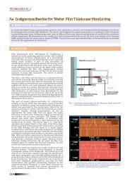
SCIENCE-37<br />
<strong>Mapping</strong> <strong>Conductivity</strong> <strong>of</strong> <strong>Graphene</strong> <strong>Sheets</strong><br />
<strong>using</strong> <strong>Conducting</strong> <strong>Tip</strong> <strong>of</strong> Atomic Force Microscopy<br />
EXECUTIVE SUMMARY<br />
Conductive tip <strong>of</strong> Atomic Force microscopy (AFM) has been used to map the local conductivity <strong>of</strong> graphene sheets. It has<br />
been observed that the conductivity <strong>of</strong> graphene sheets is higher when they are loosely bound to the underlying bulk<br />
graphite. It has also been observed that zig-zag edges show sharp rise in current than the arm-chair edges indicating<br />
enhanced electronic density <strong>of</strong> states at the Fermi energy <strong>of</strong> the zig-zag edges than the arm-chair edges.<br />
OUTLINE<br />
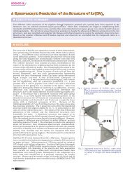
Highly oriented pyrolytic graphite (HOPG) is a<br />
periodical stack <strong>of</strong> two-dimensional (2D) graphene<br />
sheets (layers) along the c axis. Each sheet<br />
comprises hexagonal lattice <strong>of</strong> carbon bonded by<br />
2<br />
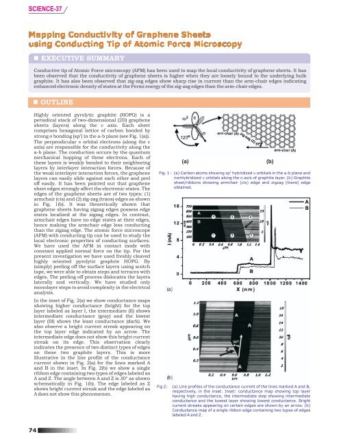
strong bonding (sp ) in the a-b plane (see Fig. 1(a)).<br />
The perpendicular orbital electrons (along the c<br />
axis) are responsible for the conductivity along the<br />
a-b plane. The conduction occurs by the quantum<br />
mechanical hopping <strong>of</strong> these electrons. Each <strong>of</strong><br />
these layers is weakly bonded to their neighboring<br />
layers by interlayer interaction forces. Because <strong>of</strong><br />
the weak interlayer interaction forces, the graphene<br />
layers can easily slide against each other and peel<br />
<strong>of</strong>f easily. It has been pointed out that graphene<br />
sheet edges strongly affect the electronic states. The<br />
edges <strong>of</strong> the graphene sheets are <strong>of</strong> two types: (1)<br />
armchair (cis) and (2) zig-zag (trans) edges as shown<br />
in Fig. 1(b). It was theoretically shown that<br />
graphene sheets having zigzag edges possess edge<br />
states localized at the zigzag edges. In contrast,<br />
armchair edges have no edge states at their edges,<br />
hence making the armchair edge less conducting<br />
than the zigzag edge. The atomic force microscope<br />
(AFM) with conducting tip can be used to study the<br />
local electronic properties <strong>of</strong> conducting surfaces.<br />
We have used the AFM in contact mode with<br />
constant applied normal force on the tip. For the<br />
present investigation we have used freshly cleaved<br />
highly oriented pyrolytic graphite HOPG. By<br />
(simply) peeling <strong>of</strong>f the surface layers <strong>using</strong> scotch<br />
tape, we were able to obtain steps and terraces with<br />
edges. The peeling <strong>of</strong>f process dislocates the layers<br />
laterally and vertically. We have studied only<br />
monolayer steps to avoid complexity in the electrical<br />
analysis.<br />
In the inset <strong>of</strong> Fig. 2(a) we show conductance maps<br />
showing higher conductance (bright) for the top<br />
layer labeled as layer I, the intermediate (II) shows<br />
intermediate conductance (gray) and the lowest<br />
layer (III) shows the least conductance (dark). We<br />
also observe a bright current streak appearing on<br />
the top layer edge indicated by an arrow. The<br />
intermediate edge does not show this bright current<br />
streak on its edge. This observation clearly<br />
indicates the presence <strong>of</strong> two distinct types <strong>of</strong> edges<br />
on these two graphite layers. This is more<br />
illustrative in the line pr<strong>of</strong>ile <strong>of</strong> the conductance<br />
current shown in Fig. 2(a) for the lines marked A<br />
and B in the inset. In Fig. 2(b) we show a single<br />
ribbon edge containing two types <strong>of</strong> edges labeled as<br />
A and Z. The angle between A and Z is 30° as shown<br />
schematically in Fig. 1(b). The edge labeled as Z<br />
shows bright current streak and the edge labeled as<br />
A does not show this phenomenon.<br />
(a)<br />
2<br />
Fig. 1 : (a) Carbon atoms showing sp hybridized orbitals in the a-b plane and<br />
nonhybridized orbitals along the c-axis <strong>of</strong> graphite layer. (b) Graphite<br />
sheet/ribbons showing armchair (cis) edge and zigzag (trans) edge<br />
obtained.<br />
Fig 2: (a) Line pr<strong>of</strong>iles <strong>of</strong> the conductance current <strong>of</strong> the lines marked A and B,<br />
respectively, in the inset. Inset: conductance map showing top layer<br />
having high conductance, the intermediate step showing intermediate<br />
conductance and the lowest layer showing lowest conductance. Bright<br />
current streaks appearing on certain edges are shown by an arrow. (b)<br />
Conductance map <strong>of</strong> a single ribbon edge containing two types <strong>of</strong> edges<br />
labeled A and Z.<br />
(b)<br />
74
SCIENCE-37<br />
ADDITIONAL INFORMATION ABOUT GRAPHENE EDGES<br />
The peeling <strong>of</strong> the layers was performed manually in an uncontrolled fashion. This can lead to different degrees <strong>of</strong> applied<br />
stress on different layers and cause different amounts <strong>of</strong> vertical displacement. The one which has a larger step height (caxis<br />
distance) will be less bound ca<strong>using</strong> large orbital overlap along the plane than the ribbon which has a lower step<br />
height (c-axis value). We motivate this schematically in Fig. 3. The difference in conductance among the steps can be<br />
explained invoking the argument that the loosely bound ribbons are more conducting than the tightly bound layers for the<br />
reasons given above.<br />
GENERAL EXPLANATION FOR THE ANOMALOUS CONDUCTIVITY<br />
Now, we will discuss the presence <strong>of</strong> sharp<br />
current peaks observed at the edges shown in the<br />
inset <strong>of</strong> Fig.2(a) and the Z region marked by arrow<br />
in Fig. 2(b). As mentioned earlier, there are<br />
mainly two types <strong>of</strong> edges formed on graphene<br />
sheets when it is cut. Recently, detailed<br />
theoretical calculations have shown that zigzag<br />
edges have edge states localized at the edges<br />
having a higher electron density. Hence these<br />
edges will have higher electrical conductance.<br />
Thus, during the mapping <strong>of</strong> the local<br />
conductance these edges will show up as brighter<br />
streaks. The layers can be oriented in a different<br />
direction with respect to each other and during<br />
the tearing process it will tear along any suitable<br />
(either zigzag or armchair) direction as we observe<br />
in Fig. 2(a). As mentioned earlier, the armchair<br />
edges have no electronic edge states and thus<br />
show no sharp peak in the current at its edges.<br />
Thus, we can say that the edges A are armchair<br />
edges and the edge Z is the zigzag edge in Fig. 2(b)<br />
(see Fig. 1(b) which shows the angle between the<br />
O<br />
armchair and the zigzag is 30 ). The<br />
enhancement <strong>of</strong> the conductance <strong>of</strong> the graphene<br />
sheets depends on the degree <strong>of</strong> dislodgement <strong>of</strong><br />
the layers. The larger the dislodgement <strong>of</strong> the<br />
layer the more enhanced is the electrical<br />
conductivity. The increase in the conductivity <strong>of</strong><br />
these sheets can be explained only by assuming<br />
that the p electrons on the loosely bound sheets<br />
are not much involved in the binding between the<br />
layers and hence would have higher mobility<br />
leading to higher electrical conductivity <strong>of</strong> the<br />
sheet.<br />
Fig. 3: Schematic representation <strong>of</strong> graphite layer separations C<br />
2>C 1>C bulk. The<br />
top layer is loosely bound showing the electrons/orbitals are spread out<br />
more along the a-b plane ca<strong>using</strong> increase in the overlap <strong>of</strong> the orbitals<br />
leading to higher conductivity.<br />
BRIEF DESCRIPTION OF THEORETICAL BACKGROUND<br />
All the above experimental electronic property we could evaluate <strong>using</strong> a density functional theory (DFT) with B3LYP/6-<br />
31G(d,p) method. This aspect have been presented in an oral presentation in ICMAT 2007, Singapore and the DFT<br />
calculation has been submitted for publication ( J. Computational Material Science).<br />
ACHIEVEMENT<br />
It has been shown here for the first time <strong>using</strong> conducting tip AFM that indeed the zig-zag edge has higher density <strong>of</strong> state<br />
at the Fermi energy than the arm-chair edge as predicted by theoretical studies. It has also been shown that isolated<br />
graphene sheets are more conducting than when they are in the bulk. This interesting conducting property <strong>of</strong> graphene<br />
sheets can be used for carbon based electronic devices.<br />
PUBLICATIONS ARISING OUT OF THIS STUDY AND RELATED WORK<br />
1. S. Banerjee, M. Sardar, N. Gayathri, A. K. Tyagi and Baldev Raj, Appl. Phys. Lett., 88 (2006) 062111.<br />
2. S. Banerjee, M. Sardar, N. Gayathri, A. K. Tyagi and Baldev Raj, Phys. Rev. B., 72 (2005) 075418.<br />
Further inquiries:<br />
Dr. S.Banerjee and Dr. A.K. Tyagi, Materials Science Division<br />
Metallurgy and Materials Group, IGCAR, e-mail:akt@igcar.gov.in<br />
75