GAIA SATA DOM HSV40(R10/R14), Left hand side 7-Pin Vertical
GAIA SATA DOM HSV40(R10/R14), Left hand side 7-Pin Vertical
GAIA SATA DOM HSV40(R10/R14), Left hand side 7-Pin Vertical

You also want an ePaper? Increase the reach of your titles
YUMPU automatically turns print PDFs into web optimized ePapers that Google loves.
Datasheet<br />
<strong>GAIA</strong> <strong>SATA</strong> DiskOnModule<br />
HSH40(<strong>R10</strong>/<strong>R14</strong>) Series<br />
(<strong>Left</strong> <strong>hand</strong> <strong>side</strong> 7-<strong>Pin</strong> Horizontal <strong>SATA</strong> <strong>DOM</strong>)<br />
090810002000<br />
Rev. A.0 Aug. 2009
Datasheet<br />
Table of Contents<br />
1. Product Description ...........................................................................................................1<br />
1.1 Product Overview........................................................................................................................................1<br />
1.2 Product Features ........................................................................................................................................1<br />
1.3 System Requirement ..................................................................................................................................1<br />
2. Specification .......................................................................................................................2<br />
2.1 Physical Specifications................................................................................................................................2<br />
2.2 Electronic Specifications .............................................................................................................................3<br />
2.3 Performance Specifications ........................................................................................................................4<br />
2.4 Environmental Specifications......................................................................................................................4<br />
2.5 Reliability Specifications..............................................................................................................................5<br />
2.6 Compliance Specifications..........................................................................................................................5<br />
3. Function ..............................................................................................................................6<br />
3.1 <strong>Pin</strong> Signal Assignment ................................................................................................................................6<br />
3.2 DiskOnModule Capacity and Cylinder, Head, Sector .................................................................................6<br />
3.3 Support ATA Commands.............................................................................................................................6<br />
4. Installation.........................................................................................................................41<br />
4.1 Installation.................................................................................................................................................41<br />
4.2 Partition.....................................................................................................................................................41<br />
4.3 Format.......................................................................................................................................................42<br />
5. Troubleshooting ...............................................................................................................43<br />
5.1 BIOS can not identify <strong>SATA</strong> DiskOnModule..............................................................................................43<br />
5.2 <strong>SATA</strong> <strong>DOM</strong> can not boot the system.........................................................................................................43<br />
6. Ordering Information........................................................................................................44<br />
7. Contact Information..........................................................................................................45<br />
Rev. A.0 Aug. 2009
Datasheet<br />
List of Figures<br />
Figure 1: <strong>Left</strong> <strong>hand</strong> <strong>side</strong> 7-<strong>Pin</strong> Horizontal <strong>SATA</strong> DiskOnModule Overlook Diagram .......................................2<br />
Figure 2: <strong>Left</strong> <strong>hand</strong> <strong>side</strong> 7-<strong>Pin</strong> Horizontal <strong>SATA</strong> <strong>DOM</strong> Dimensions.................................................................2<br />
Figure 3: <strong>SATA</strong> DiskOnModule Block Diagram ...............................................................................................3<br />
Figure 4: <strong>SATA</strong> Signal Connector ....................................................................................................................6<br />
Rev. A.0 Aug. 2009
Datasheet<br />
List of Table<br />
Table 1: 7-<strong>Pin</strong> Horizontal <strong>SATA</strong> DiskOnModule Physical Dimension ..............................................................2<br />
Table 2: Serial ATA connector pin definitions...................................................................................................6<br />
Table 3: DiskOnModule Capacity and Cylinder, Head, Sector........................................................................6<br />
Table 4: ATA Command Set.............................................................................................................................6<br />
Table 5: Diagnostic Codes...............................................................................................................................9<br />
Table 6: Identify Device Information ..............................................................................................................10<br />
Table 7: Extended Error Codes .....................................................................................................................25<br />
Table 8: Feature Supported...........................................................................................................................26<br />
Table 9: Transfer mode values ......................................................................................................................26<br />
Table 10: Advanced power management levels............................................................................................27<br />
Table 11: SMART Feature register values.....................................................................................................29<br />
Table 12: Device SMART Data Structure ......................................................................................................31<br />
Table 13: Translate Sector Information..........................................................................................................36<br />
Table 14: <strong>Left</strong> <strong>hand</strong> <strong>side</strong> 7-<strong>Pin</strong> Horizontal <strong>SATA</strong> DiskOnModule Ordering Information.................................44<br />
Rev. A.0 Aug. 2009
Datasheet<br />
Revision Date Major Changes<br />
1.0 2009/6/2 1. Preliminary<br />
A.0 2009/8/6 1. Formal Release<br />
Copyright Information<br />
Copyright © 2009, CoreSolid Storage Corporation. All rights reserved.<br />
The information and specifications provided in this document should be used for comparative analysis and<br />
reference purposes. The content of this document is subject to change without prior notice.<br />
Rev. A.0 Aug. 2009
<strong>SATA</strong> DiskOnModule<br />
1. Product Description<br />
1.1 Product Overview<br />
CoreSolid Storage’s <strong>SATA</strong> DiskOnModule (<strong>DOM</strong>) is the storage device based on NAND flash memory technology. This<br />
product complies Serial ATA standard interface and is suitable for data storage media and code storage device for<br />
embedded system and boot disk. By using <strong>SATA</strong> DiskOnModule, it is possible to operate good performance for the<br />
systems, which have <strong>SATA</strong> interface.<br />
With small form factor, the applicable appliance can add or install <strong>SATA</strong> storage device on its Mother Board or<br />
Complete set.<br />
Application Fields:<br />
- Industrial PC and Thin Client<br />
- Game and Telecommunication Machine<br />
- Ticketing, Examining, testing machine<br />
- Army, Health and Production Equipment and Machine<br />
- Other machines and Equipments with Serial ATA 3.0Gb/s Interface.<br />
1.2 Product Features<br />
- Small form factor with Serial ATA Standard Interface connector<br />
- Memory Capacities: 128MB ~ 16GB<br />
- High performance and reliability<br />
- Noiseless and stable installation to system<br />
- Operating voltage only 5V operation<br />
- Standard Serial ATA Interface<br />
- Operating as Boot Disk<br />
- Code Storage Device for Embeded Operating System<br />
1.3 System Requirement<br />
- The Host system which is connected to <strong>SATA</strong> DiskOnModule should meet system requirements at minimum;<br />
1.3.1 Power Requirement<br />
- Voltage: DC +5V ± 5%<br />
1.3.2 Operating System<br />
- Windows 2000/XP/Vista<br />
- Linux<br />
- DOS<br />
- WinXP Embedded<br />
- WinCE<br />
1.3.3 Interface<br />
- Standard <strong>SATA</strong> 3.0Gb/s Interface<br />
Rev. A.0 1/45 Aug. 2009
<strong>SATA</strong> DiskOnModule<br />
2. Specification<br />
2.1 Physical Specifications<br />
2.1.1 Overlook<br />
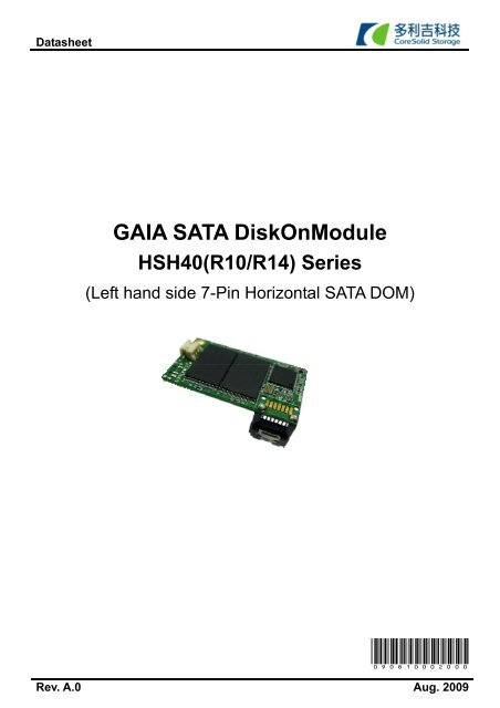
The overlook views of left <strong>hand</strong> <strong>side</strong> 7-<strong>Pin</strong> Horizontal <strong>SATA</strong> DiskOnModule HSH40(<strong>R10</strong>/<strong>R14</strong>) are illustrated in<br />
Figure 1. HSH40(<strong>R10</strong>/<strong>R14</strong>) is a left <strong>hand</strong> <strong>side</strong> 7-<strong>Pin</strong> Horizontal <strong>SATA</strong> DiskOnModule .<br />
HSH40(<strong>R10</strong>/<strong>R14</strong>) Front View<br />
HSH40(<strong>R10</strong>/<strong>R14</strong>) Rear View<br />
Power Jack<br />
<strong>SATA</strong> Interface Connector<br />
2.1.2 Dimension<br />
Figure 1: <strong>Left</strong> <strong>hand</strong> <strong>side</strong> 7-<strong>Pin</strong> Horizontal <strong>SATA</strong> DiskOnModule Overlook Diagram<br />
The Dimensions of left <strong>hand</strong> <strong>side</strong> 7-<strong>Pin</strong> Horizontal <strong>SATA</strong> DiskOnModule are illustrated in Figure 2 and described in<br />
Table 1.<br />
Figure 2: <strong>Left</strong> <strong>hand</strong> <strong>side</strong> 7-<strong>Pin</strong> Horizontal <strong>SATA</strong> <strong>DOM</strong> Dimensions<br />
Table 1: 7-<strong>Pin</strong> Horizontal <strong>SATA</strong> DiskOnModule Physical Dimension<br />
Length<br />
45.0 ± 0.15 mm<br />
Width<br />
Thickness<br />
24.9 ± 0.15 mm<br />
15.0 ± 0.15mm<br />
2.1.3 Weight<br />
- Weight: < 7.6g<br />
Rev. A.0 2/45 Aug. 2009
<strong>SATA</strong> DiskOnModule<br />
2.2 Electronic Specifications<br />
2.2.1 Product Definition<br />
<strong>SATA</strong> DiskOnModule is designed to operate and work as Data or Code Storage device by NAND Flash Memory<br />
and its Controller through Standard Serial ATA 3.0Gb/s Interface to Host Systems.<br />
Regulator<br />
VCC<br />
Vcore<br />
Flash<br />
Controller<br />
Flash memory<br />
VCC<br />
Data<br />
Buffer<br />
<strong>SATA</strong><br />
Interface<br />
A+<br />
A-<br />
B+<br />
X`tal<br />
Control signal<br />
Data<br />
Flash<br />
Array<br />
B-<br />
Figure 3: <strong>SATA</strong> DiskOnModule Block Diagram<br />
2.2.2 Operating Voltage<br />
- Voltage DC +5V ± 5%<br />
2.2.3 Capacity and Block Size information<br />
- Capacity: 128MB ~ 16GB<br />
- Sector Size: 512Bytes<br />
2.2.4 Power Consumption<br />
- DC Information<br />
Read:
<strong>SATA</strong> DiskOnModule<br />
2.3 Performance Specifications<br />
2.3.1 Modes<br />
- Serial ATA 3.0Gb/s<br />
2.3.2 Access Time<br />
- <strong>SATA</strong> DiskOnModule’s maximum access time is about 0.3msec.<br />
※ Testing Platform<br />
Testing S/W: HD Tune 2.53, Testing OS: WinXP<br />
Mother-Board: ASUS P5GC-FX, CPU: Core2Dual 1.60G, Chipset: Intel 945G+ICH7, Main Memory: DDR2-400 2GB<br />
Testing base: Time required Between Host to Device<br />
2.3.3 Seek Time<br />
- <strong>SATA</strong> DiskOnModule has no seek time by being based on Flash Memory technology.<br />
2.3.4 Mount Time<br />
The Mount Time for initializing and mounting <strong>SATA</strong> DiskOnModule is different by depending on Operating System and<br />
testing Platform.<br />
2.3.5 Data Transfer Time<br />
- Sequential Read: up to 20 MB/sec, or 40MB/sec for Dual mode<br />
- Sequential Write: up to 10 MB/sec, or 20MB/sec for Dual mode<br />
※ Test Platform: Average Value based on Serial ATA 3.0Gb/s interface<br />
Mother-Board: ASUS P5GC-FX, CPU: Core2Dual 1.60G, Chipset: Intel 945G+ICH7, Main Memory: DDR2-400 2GB<br />
Testing Software: HD Bench 3.4 Testing OS: Windows XP<br />
Notice:<br />
The value is various bases on the testing platform.<br />
2.3.6 Data Retention<br />
- 10years without requiring power support<br />
Notice:<br />
The Value of Data Retention is various bases on the type and manufacturer of Flash Memory<br />
2.3.7 Wear-leveling<br />
- Static Wear-Leveling for same level of Write/Erase Cycle<br />
2.3.8 Bad Block Management<br />
- The Bad Blocks of Flash Memory will be replaced into new ones by controller.<br />
2.4 Environmental Specifications<br />
2.4.1 Temperature<br />
• Operating Temperature: 0°C to +70°C, Storage Temperature: -40°C to +85°C.<br />
2.4.2 Humidity<br />
• Operating Humidity (30°C Max. Wet Bulb Temp): 10% to 95%.<br />
• Non-Operating Humidity (30°C Max. Wet Bulb Temp): 10% to 95% (with no condensation relative humidity).<br />
2.4.3 Bare Drop test<br />
• Test Conditions : 75cm height<br />
• Test Orientation : (Free fell) Front/Rear/Right/<strong>Left</strong>/Top/Bottom <strong>side</strong><br />
Rev. A.0 4/45 Aug. 2009
<strong>SATA</strong> DiskOnModule<br />
2.4.4 Vibration<br />
• Random Vibration(Operation) : Test Specification<br />
Frequency(Hz) PSD(G2/Hz) Acceleration (Grms) Dwell Time (Min)<br />
10 0.01<br />
100 0.08<br />
6Grms<br />
500 0.08<br />
• Sine Vibration(Non-Operation) : Test Specification<br />
30min per axis<br />
(X,Y,Z)<br />
Frequency(Hz) PSD(G2/Hz) Acceleration (G) Dwell Time (Min)<br />
10 0.01<br />
100 0.04<br />
500 0.04<br />
2000 0.004<br />
15Grms<br />
30min per axis<br />
(X,Y,Z)<br />
2.5 Reliability Specifications<br />
2.5.1 ECC/EDC (Error Correction Code/Error Detection Code)<br />
• Built-in Reed Solomon 4symbol/512 bytes<br />
2.5.2 MTTF (Mean Time To Failure)<br />
• TBD<br />
Notice: The Value of MTTF is based on the specific access size, access period, and type and manufacturer of Flash Memory.<br />
2.5.3 Power Cycle<br />
• The abnormal Power Cycling test is all pass for 3000 loops.<br />
2.6 Compliance Specifications<br />
- CE<br />
- FCC<br />
Rev. A.0 5/45 Aug. 2009
<strong>SATA</strong> DiskOnModule<br />
3. Function<br />
3.1 <strong>Pin</strong> Signal Assignment<br />
The signals assigned for Serial ATA applications are described in Table 2<br />
Table 2: Serial ATA connector pin definitions<br />
Segment <strong>Pin</strong> No Function Definition<br />
Signal<br />
S1 Gnd <strong>Pin</strong> 1<br />
S2 A+<br />
Differential signal pair A from Phy<br />
S3 A-<br />
S4<br />
Gnd<br />
S5 B-<br />
Differential signal pair B from Phy<br />
S6 B+<br />
S7<br />
Gnd<br />
Notice: All pins are a 1.27 mm (0.050”) pitch.<br />
3.2 DiskOnModule Capacity and Cylinder, Head, Sector<br />
Figure 4: <strong>SATA</strong> Signal Connector<br />
.<br />
The table 3 show various capacities available for HSH40 series, if your platform does not support auto-detection<br />
function or HSH40 series is not identified, we advice can following below Cylinders, Heads, Sectors number to setting<br />
your platform.<br />
Unformatted Disk<br />
Capacity<br />
Table 3: DiskOnModule Capacity and Cylinder, Head, Sector<br />
No. of<br />
Cylinders<br />
No. of<br />
Heads<br />
No. of<br />
Sectors<br />
Disk Total Sector<br />
128MB 994 8 32 254464<br />
256MB 974 16 32 498688<br />
512MB 1,012 16 63 1,020,096<br />
1GB 1,984 16 63 1,999,872<br />
2GB 3,980 16 63 4,011,840<br />
4GB 7,970 16 63 8,033,760<br />
8GB 15,945 16 63 16,072,560<br />
The following capacity are in LBA mode<br />
16GB 16,383 16 63 32,165,280<br />
3.3 Support ATA Commands<br />
• ATA Command Set<br />
- ATA Command Set summarizes the ATA command set with the paragraphs that follow describing the<br />
individual commands and the task file for each.<br />
Table 4: ATA Command Set<br />
No COMMAND Code FR SC SN CY DH LBA<br />
1 Check Power Mode E5h or 98h - - - - D -<br />
2 Erase Sector(s) C0h - Y Y Y Y Y<br />
3 Execute Drive Diagnostic 90h - - - - D -<br />
4 Flush Cache E7h - - - - D -<br />
5 Format Track 50h - Y - Y Y Y<br />
6 Identify Device ECh - - - - D -<br />
7 Identify Device DMA EEh - - - - D -<br />
8 Idle E3h or 97h - Y - - D -<br />
Rev. A.0 6/45 Aug. 2009
<strong>SATA</strong> DiskOnModule<br />
No COMMAND Code FR SC SN CY DH LBA<br />
9 Idle Immediate E1h or 95h - - - - D -<br />
10 Initialize Drive Parameters 91h - Y - - Y -<br />
11 Media Lock DEh - - - - D -<br />
12 Media Unlock DFh - - - - D -<br />
13 NOP 00h - - - - D -<br />
14 Read Buffer E4h - - - - D -<br />
15 Read DMA C8h - Y Y Y Y Y<br />
16 Read Long Sector 22h or 23h - - Y Y Y Y<br />
17 Read Multiple C4h - Y Y Y Y Y<br />
18 Read Native Max Address F8h - - - - D -<br />
19 Read Sector(s) 20h or 21h - Y Y Y Y Y<br />
20 Read Verify Sector(s) 40h or 41h - Y Y Y Y Y<br />
21 Recalibrate 1Xh - - - - D -<br />
22 Request Sense 03h - - - - D -<br />
23 Seek 7Xh - - Y Y Y Y<br />
24 Set Features EFh Y - - - D -<br />
25 Set Max Address F9h - Y Y Y Y Y<br />
26 Set Multiple Mode C6h - Y - - D -<br />
27 Set Sleep Mode E6h or 99h - - - - D -<br />
28 SMART B0h Y Y - Y Y -<br />
29 Standby E2h or 96h - - - - D -<br />
30 Standby Immediate E0h or 94h - - - - D -<br />
31 Translate Sector 87h - Y Y Y Y Y<br />
32 Write Buffer E8h - - - - D -<br />
33 Write DMA CAh - Y Y Y Y Y<br />
34 Write Long Sector 32h or 33h - - Y Y Y Y<br />
35 Write Multiple C5h - Y Y Y Y Y<br />
36 Write Multiple w/o Erase CDh - Y Y Y Y Y<br />
37 Write Sector(s) 30h or 31h - Y Y Y Y Y<br />
38 Write Sector(s) w/o Erase 38h - Y Y Y Y Y<br />
39 Write Verify 3Ch - Y Y Y Y Y<br />
Definitions:<br />
FR = Features Register<br />
SC = Sector Count Register <br />
SN = Sector Number Register <br />
CY = Cylinder Registers<br />
DH = Device/Drive/Head Register<br />
LBA = Logical Block Address Mode Supported (see command descriptions for use).<br />
Y - The register contains a valid parameter for this command. For the Drive/Head Register Y means both the device<br />
and head parameters are used.<br />
D - Only the device parameter is valid and not the head parameter;<br />
C - The register contains command specific data (see command descriptions for use).<br />
Rev. A.0 7/45 Aug. 2009
<strong>SATA</strong> DiskOnModule<br />
(1) Check Power Mode - 98h or E5h<br />
Bit -> 7 6 5 4 3 2 1 0<br />
Command<br />
98h or E5h<br />
C/D/H (6) X Drive X<br />
Cyl High (5)<br />
X<br />
Cyl Low (4)<br />
X<br />
Sec Num (3)<br />
X<br />
Sec Cnt (2)<br />
X<br />
Feature (1)<br />
X<br />
Check Power Mode<br />
This command checks the power mode.<br />
If the device is in, going to, or recovering from the sleep mode, the device sets BSY, sets the Sector Count<br />
Register to 00h, clears BSY and generates an interrupt.<br />
If the device is in Idle mode, the device sets BSY, sets the Sector Count Register to FFh, clears BSY and<br />
generates an interrupt.<br />
(2) Erase Sector(s) - C0h<br />
Bit -> 7 6 5 4 3 2 1 0<br />
Command<br />
C0h<br />
C/D/H (6) 1 LBA 1 Drive Head (LBA 27-24)<br />
Cyl High (5) Cylinder High (LBA 23-16)<br />
Cyl Low (4) Cylinder Low (LBA 15-8)<br />
Sec Num (3) Sector Number (LBA 7-0)<br />
Sec Cnt (2)<br />
Sector Count<br />
Feature (1)<br />
X<br />
Erase Sector<br />
This command is used to pre-erase and condition data sectors in advance of a Write without Erase or Write<br />
Multiple without Erase command. There is no data transfer associated with this command but a Write Fault error status<br />
can occur.<br />
(3) Execute Drive Diagnostic - 90h<br />
Bit -> 7 6 5 4 3 2 1 0<br />
Command<br />
90h<br />
C/D/H (6) X Drive X<br />
Cyl High (5)<br />
X<br />
Cyl Low (4)<br />
X<br />
Sec Num (3)<br />
X<br />
Sec Cnt (2)<br />
X<br />
Feature (1)<br />
X<br />
Execute Drive Diagnostic<br />
This command performs the internal diagnostic tests implemented by the device.<br />
When the diagnostic command is issued, the Drive bit is ignored and the diagnostic command is executed by both<br />
the Master and the Slave with the Master responding with status for both devices.<br />
The Diagnostic codes shown in Table 5: Diagnostic Codes are returned in the Error Register at the end of the<br />
command.<br />
Rev. A.0 8/45 Aug. 2009
<strong>SATA</strong> DiskOnModule<br />
Code<br />
01h<br />
02h<br />
03h<br />
04h<br />
05h<br />
8Xh<br />
Table 5: Diagnostic Codes<br />
No Error Detected<br />
Formatter Device Error<br />
Sector Buffer Error<br />
ECC Circuitry Error<br />
Controlling Microprocessor Error<br />
Slave Error in True IDE Mode<br />
Error Type<br />
(4) Flush Cache – E7h<br />
Bit -> 7 6 5 4 3 2 1 0<br />
Command<br />
E7h<br />
C/D/H (6) X X X Drive X<br />
Cyl High (5)<br />
X<br />
Cyl Low (4)<br />
X<br />
Sec Num (3)<br />
X<br />
Sec Cnt (2)<br />
X<br />
Feature (1)<br />
X<br />
Flush Cache<br />
This command is used by the host to request the device to flush the write cache. If there is data in the write cache,<br />
that data shall be written to the Flash memory. The BSY bit shall remain set to one until all data has been successfully<br />
written or an error occurs.<br />
(5) Format Track - 50h<br />
Bit -> 7 6 5 4 3 2 1 0<br />
Command<br />
50h<br />
C/D/H (6) 1 LBA 1 Drive Head (LBA 27-24)<br />
Cyl High (5) Cylinder High (LBA 23-16)<br />
Cyl Low (4) Cylinder Low (LBA 15-8)<br />
Sec Num (3) X (LBA 7-0)<br />
Sec Cnt (2)<br />
Count (LBA mode only)<br />
Feature (1)<br />
X<br />
Format Track<br />
This command writes the desired head and cylinder of the selected drive with a vendor unique data pattern<br />
(typically FFh or 00h). To remain host backward compatible, the device expects a sector buffer of data from the host to<br />
follow the command with the same protocol as the Write Sector(s) command although the information in the buffer is<br />
not used by the device. If LBA=1 then the number of sectors to format is taken from the Sec Cnt register (0=256). The<br />
use of this command is not recommended.<br />
Rev. A.0 9/45 Aug. 2009
<strong>SATA</strong> DiskOnModule<br />
(6) Identify Device – ECh<br />
Bit -> 7 6 5 4 3 2 1 0<br />
Command<br />
ECh<br />
C/D/H (6) X X X Drive X<br />
Cyl High (5)<br />
X<br />
Cyl Low (4)<br />
X<br />
Sec Num (3)<br />
X<br />
Sec Cnt (2)<br />
X<br />
Feature (1)<br />
X<br />
Identify Device<br />
The Identify Device command enables the host to receive parameter information from the device. This command<br />
has the same protocol as the Read Sector(s) command. The parameter words in the buffer have the arrangement and<br />
meanings defined in Table 6. All reserved bits or words are zero. Hosts should not depend on obsolete words in Identify<br />
Device containing 0. Table 6 specifies each field in the data returned by the Identify Device Command. In Table 6, X<br />
indicates a numeric nibble value specific to the device and aaaa indicates an ASCII string specific to the particular<br />
drive.<br />
Word<br />
Address<br />
Table 6: Identify Device Information<br />
Default<br />
Value<br />
Total<br />
Bytes<br />
Data Field Type Information<br />
0 0XXX 2 General configuration – Bit Significant with ATA definitions.<br />
1 XXXXh 2 Default number of cylinders<br />
2 0000h 2 Reserved<br />
3 00XXh 2 Default number of heads<br />
4 0000h 2 Reserved for vendor<br />
5 0200h 2 Reserved for vendor<br />
6 XXXXh 2 Default number of sectors per track<br />
7-8 XXXXh 4 Reserved for assignment by the CFA<br />
9 0000h 2 Reserved<br />
10-19 aaaa 20 Serial number in ASCII (Right Justified)<br />
20 0002h 2 Reserved for vendor<br />
21 000Xh 2 Reserved for vendor<br />
22 0004h 2 Reserved for vendor<br />
23-26 aaaa 8 Firmware revision in ASCII. Big Endian Byte Order in Word<br />
27-46 aaaa 40 Model number in ASCII (<strong>Left</strong> Justified) Big Endian Byte Order in Word<br />
47 800Xh 2 Maximum number of sectors on Read/Write Multiple command<br />
48 0000h 2 Reserved<br />
49 0F00h 2 Capabilities: DMA, LBA, IORDY supported<br />
50 0000h 2 Capabilities: Others, Fixed<br />
51 0200h 2 PIO data transfer cycle timing mode 2<br />
52 0000h 2 Reserved<br />
53 0007h 2 Data Fields 54 to 58, 64 to 70 and 88 are valid<br />
54 XXXXh 2 Current numbers of cylinders<br />
55 XXXXh 2 Current numbers of heads<br />
56 XXXXh 2 Current sectors per track<br />
57-58 XXXXh 4 Current capacity in sectors (LBAs)(Word 57 = LSW, Word 58 = MSW)<br />
59 010Xh 2 Multiple sector setting<br />
60-61 XXXXh 4 Total number of sectors addressable in LBA Mode<br />
Rev. A.0 10/45 Aug. 2009
<strong>SATA</strong> DiskOnModule<br />
Word<br />
Address<br />
Default<br />
Value<br />
Total<br />
Bytes<br />
Data Field Type Information<br />
62 0000h 2 Reserved<br />
63 0X0Xh 2 Multiword DMA transfer.<br />
64 0003h 2 Advanced PIO modes 3 and 4 supported<br />
65 0078h 2 Minimum Multiword DMA transfer cycle time per word.<br />
66 0078h 2 Recommended Multiword DMA transfer cycle time.<br />
67 0078h 2 Minimum PIO transfer cycle time without flow control<br />
68 0078h 2 Minimum PIO transfer cycle time with IORDY flow control<br />
69-79 0000h 20 Reserved<br />
80 0020h 2 Major version number, ATA-5 support<br />
81 0000h 2 Minor version number, not reported<br />
82 7409h 2 Features/command sets supported (NOP, SMART,…)<br />
83 5004h 2 Features/command sets supported (Flush Cache, …)<br />
84 4000h 2 Features/command sets supported (extension)<br />
85 740Xh 2 Features/command sets enabled (NOP, SMART,…)<br />
86 X004h 2 Features/command sets enabled (Flush Cache, …)<br />
87 4000h 2 Features/command sets enabled (extension)<br />
88 XXXXh 2 Ultra DMA Mode Supported and Selected<br />
89-92 0000h 8 Reserved<br />
93 XXXXh 2 Hardware Reset result<br />
94-129 0000h 72 Reserved<br />
130-152 XXXXh 8 Reserved for vendor<br />
153-159 0000h 12 Reserved<br />
160 A064h 2 Power requirement description<br />
161-175 XXXXh 2 Reserved for assignment by the CFA<br />
176-254 0000h 180 Reserved<br />
255 XXA5h 2 Integrity Word<br />
Word 0: General Configuration<br />
This field indicates the general characteristics of the device.<br />
Bit 15-12: Configuration Flag: It is fixed as 0 to represent it is an ATA device.<br />
Bits 11-8: Retired. These bits have retired ATA bit definitions. It is recommended that the value of these bits<br />
be either the preferred value of 0h or the value of 4h that preserves the corresponding bits to one or zero.<br />
Bit 7: Removable Media Device If Bit 7 is set to 1, the device contains media that can be removed during<br />
device operation. If Bit 7 is set to 0, the device contains non-removable media.<br />
Bit 6: Not Removable Controller and/or Device<br />
Alert!<br />
This bit will be con<strong>side</strong>red for obsolescence in a future revision of this standard.<br />
If Bit 6 is set to 1, the Device is intended to be nonremovable during operation. If Bit 6 is set to 0, the<br />
Device is intended to be removable during operation.<br />
Bits 5-0: Retired/Reserved<br />
Alert! Bit 2 will be con<strong>side</strong>red for definition in a future revision of this standard and shall be 0 at this time.<br />
Bits 5-1 have retired ATA bit definitions.<br />
Bit 2 shall be 0.<br />
Bit 0 is reserved and shall be 0.<br />
Rev. A.0 11/45 Aug. 2009
<strong>SATA</strong> DiskOnModule<br />
Word 1: Default Number of Cylinders<br />
This field contains the number of translated cylinders in the default translation mode. This value will be the same<br />
as the number of cylinders.<br />
Word 3: Default Number of Heads<br />
This field contains the number of translated heads in the default translation mode.<br />
Word 6: Default Number of Sectors per Track<br />
This field contains the number of sectors per track in the default translation mode.<br />
Words 10-19: Serial Number<br />
This field contains the serial number for this device and is right justified and padded with spaces (20h).<br />
Words 20: Buffer type<br />
This field contains the buffer type of the device. It is set by default.<br />
Alert! This word is con<strong>side</strong>red for obsolescence in a future revision of this standard.<br />
Words 23-26: Firmware Revision<br />
This field contains the revision of the firmware for this product.<br />
Words 27-46: Model Number<br />
This field contains the model number for this product and is left justified and padded with spaces (20h).<br />
Word 47: Read/Write Multiple Sector Count<br />
Bits 15-8 shall be the recommended value of 80h or the permitted value of 00h. Bits 7-0 of this word define the<br />
maximum number of sectors per block that the device supports for Read/Write Multiple commands.<br />
Word 49: Capabilities<br />
Bit 13: Standby Timer<br />
If bit 13 is set to 1 then the Standby timer is supported as defined by the IDLE command<br />
If bit 13 is set to 0 then the Standby timer operation is defined by the vendor.<br />
Bit 11: IORDY Supported<br />
If bit 11 is set to 1 then this device supports IORDY operation.<br />
If bit 11 is set to 0 then this device may support IORDY operation.<br />
Bit 10: IORDY may be disabled<br />
Bit 10 shall be set to 0, indicating that IORDY may not be disabled.<br />
Bit 9: LBA supported<br />
Bit 9 shall be set to 1, indicating that this device supports LBA mode addressing. Devices shall support<br />
LBA addressing.<br />
Bit 8: DMA Supported<br />
Rev. A.0 12/45 Aug. 2009
<strong>SATA</strong> DiskOnModule<br />
If bit 8 is set to 1 then Read DMA and Write DMA commands are supported.<br />
Bit 8 shall be set to 0. Read/Write DMA commands are not currently permitted on CF devices.<br />
Word 51: PIO Data Transfer Cycle Timing Mode<br />
The PIO transfer timing for each device falls into modes that have unique parametric timing specifications. The<br />
value returned in Bits 15-8 shall be 00h for mode 0, 01h for mode 1, or 02h for mode 2. Values 03h through FFh<br />
are reserved.<br />
Word 53: Translation Parameters Valid<br />
Bit 0 shall be set to 1 indicating that words 54 to 58 are valid and reflect the current number of cylinders heads and<br />
sectors. If bit 1 of word 53 is set to 1, the values in words 64 through 70 are valid. If this bit is cleared to 0, the<br />
values reported in words 64-70 are not valid. Any device that supports PIO mode 3 or above shall set bit 1 of<br />
word 53 to one and support the fields contained in words 64 through 70.<br />
Words 54-56: Current Number of Cylinders, Heads, Sectors/Track<br />
These fields contain the current number of user addressable Cylinders, Heads, and Sectors/Track in the current<br />
translation mode.<br />
Words 57-58: Current Capacity<br />
This field contains the product of the current cylinders times heads times sectors.<br />
Word 59: Multiple Sector Setting<br />
Bits 15-9 are reserved and shall be set to 0.<br />
Bit 8 shall be set to 1 indicating that the Multiple Sector Setting is valid.<br />
Bits 7-0 are the current setting for the number of sectors that shall be transferred per interrupt on Read/Write<br />
Multiple commands.<br />
Words 60-61: Total Sectors Addressable in LBA Mode<br />
This field contains the total number of user addressable sectors for the device in LBA mode only.<br />
Word 63: Multiword DMA transfer<br />
Bits 15 through 8 of word 63 of the Identify Device parameter information is defined as the Multiword DMA mode<br />
selected field. If this field is supported, bit 1 of word 53 shall be set to one. This field is bit significant. Only one of<br />
bits may be set to one in this field by the device to indicate the multiword DMA mode which is currently selected.<br />
Of these bits, bits 15 through 11 are reserved. Bit 8, if set to one, indicates that Multiword DMA mode 0 has been<br />
selected. Bit 9, if set to one, indicates that Multiword DMA mode 1 has been selected. Bit 10, if set to one,<br />
indicates that Multiword DMA mode 2 has been selected. Selection of Multiword DMA modes 3 and above are<br />
specific to device are reported in word 163 as described in Word 163: CF Advanced True IDE Timing Mode<br />
Capabilities and Settings.<br />
Bits 7 through 0 of word 63 of the Identify Device parameter information is defined as the Multiword DMA data<br />
Rev. A.0 13/45 Aug. 2009
<strong>SATA</strong> DiskOnModule<br />
transfer supported field. If this field is supported, bit 1 of word 53 shall be set to one. This field is bit significant.<br />
Any number of bits may be set to one in this field by the device to indicate the Multiword DMA modes it is<br />
capable of supporting.<br />
Of these bits, bits 7 through 2 are reserved. Bit 0, if set to one, indicates that the device supports Multiword DMA<br />
mode 0. Bit 1, if set to one, indicates that the device supports Multiword DMA modes 1 and 0. Bit 2, if set to one,<br />
indicates that the device supports Multiword DMA modes 2, 1 and 0.<br />
Support for Multiword DMA modes 3 and above are specific to device are reported in Word 163: CF Advanced True<br />
IDE Timing Mode Capabilities and Settings.<br />
Word 64: Advanced PIO transfer modes supported<br />
Bits 7 through 0 of word 64 of the Identify Device parameter information is defined as the advanced PIO data<br />
transfer supported field. If this field is supported, bit 1 of word 53 shall be set to one. This field is bit significant.<br />
Any number of bits may be set to one in this field by the device to indicate the advanced PIO modes it is capable<br />
of supporting.<br />
Of these bits, bits 7 through 2 are reserved. Bit 0, if set to one, indicates that the device supports PIO mode 3. Bit 1,<br />
if set to one, indicates that the device supports PIO mode 4.<br />
Support for PIO modes 5 and above are specific to device are reported in word 163 as described in Word 163: CF<br />
Advanced True IDE Timing Mode Capabilities and Settings.<br />
Word 65: Minimum Multiword DMA transfer cycle time<br />
Word 65 of the parameter information of the Identify Device command is defined as the minimum Multiword DMA<br />
transfer cycle time. This field defines, in nanoseconds, the minimum cycle time that, if used by the host, and the<br />
device guarantees data integrity during the transfer.<br />
If this field is supported, bit 1 of word 53 shall be set to one. The value in word 65 shall not be less than the<br />
minimum cycle time for the fastest DMA mode supported by the device. This field shall be supported by all<br />
device supporting DMA modes 1 and above.<br />
If bit 1 of word 53 is set to one, but this field is not supported, the Device shall return a value of zero in this field.<br />
Word 66: Recommended Multiword DMA transfer cycle time<br />
Word 66 of the parameter information of the Identify Device command is defined as the recommended Multiword<br />
DMA transfer cycle time. This field defines, in nanoseconds, the cycle time that, if used by the host, may<br />
optimize the data transfer from by reducing the probability that the device will need to negate the DMARQ signal<br />
during the transfer of a sector.<br />
If this field is supported, bit 1 of word 53 shall be set to one. The value in word 66 shall not be less than the value<br />
in word 65. This field shall be supported by all device supporting DMA modes 1 and above.<br />
If bit 1 of word 53 is set to one, but this field is not supported, the Device shall return a value of zero in this field.<br />
Word 67: Minimum PIO transfer cycle time without flow control<br />
Word 67 of the parameter information of the Identify Device command is defined as the minimum PIO transfer<br />
without flow control cycle time. This field defines, in nanoseconds, the minimum cycle time that, if used by the<br />
Rev. A.0 14/45 Aug. 2009
<strong>SATA</strong> DiskOnModule<br />
host, the device guarantees data integrity during the transfer without utilization of flow control.<br />
If this field is supported, Bit 1 of word 53 shall be set to one.<br />
Any device that supports PIO mode 3 or above shall support this field, and the value in word 67 shall not be less<br />
than the value reported in word 68.<br />
If bit 1 of word 53 is set to one because a device supports a field in words 64-70 other than this field and the device<br />
does not support this field, the device shall return a value of zero in this field.<br />
Word 68: Minimum PIO transfer cycle time with IORDY<br />
Word 68 of the parameter information of the Identify Device command is defined as the minimum PIO transfer with<br />
IORDY flow control cycle time. This field defines, in nanoseconds, the minimum cycle time that the device<br />
supports while performing data transfers while utilizing IORDY flow control.<br />
If this field is supported, Bit 1 of word 53 shall be set to one.<br />
Any device that supports PIO mode 3 or above shall support this field, and the value in word 68 shall be the fastest<br />
defined PIO mode supported by the device.<br />
If bit 1 of word 53 is set to one because a device supports a field in words 64-70 other than this field and the device<br />
does not support this field, the device shall return a value of zero in this field.<br />
Words 82-84: Features/command sets supported<br />
Words 82, 83, and 84 shall indicate features/command sets supported. The value 0000h or FFFFh was placed in<br />
each of these words by device prior to ATA-3 and shall be interpreted by the host as meaning that<br />
features/command sets supported are not indicated. Bits 1 through 13 of word 83 and bits 0 through 13 of word<br />
84 are reserved. Bit 14 of word 83 and word 84 shall be set to one and bit 15 of word 83 and word 84 shall be<br />
cleared to zero to provide indication that the features/command sets supported words are valid. The values<br />
in these words should not be depended on by host implementers.<br />
Bit 0 of word 82 shall be set to zero; the SMART feature set is not supported.<br />
If bit 1 of word 82 is set to one, the Security Mode feature set is supported.<br />
Bit 2 of word 82 shall be set to zero; the Removable Media feature set is not supported.<br />
Bit 3 of word 82 shall be set to one; the Power Management feature set is supported.<br />
Bit 4 of word 82 shall be set to zero; the Packet Command feature set is not supported.<br />
If bit 5 of word 82 is set to one, write cache is supported.<br />
If bit 6 of word 82 is set to one, look-ahead is supported.<br />
Bit 7 of word 82 shall be set to zero; release interrupt is not supported.<br />
Bit 8 of word 82 shall be set to zero; Service interrupt is not supported.<br />
Bit 9 of word 82 shall be set to zero; the Device Reset command is not supported.<br />
Bit 10 of word 82 shall be set to zero; the Host Protected Area feature set is not supported.<br />
Bit 11 of word 82 is obsolete.<br />
Bit 12 of word 82 shall be set to one; the device supports the Write Buffer command.<br />
Bit 13 of word 82 shall be set to one; the device supports the Read Buffer command.<br />
Bit 14 of word 82 shall be set to one; the device supports the NOP command.<br />
Bit 15 of word 82 is obsolete.<br />
Rev. A.0 15/45 Aug. 2009
<strong>SATA</strong> DiskOnModule<br />
Bit 0 of word 83 shall be set to zero; the device does not support the Download Microcode command.<br />
Bit 1 of word 83 shall be set to zero; the device does not support the Read DMA Queued and Write DMA<br />
Queued commands.<br />
Bit 2 of word 83 shall be set to one; the device supports the CFA feature set.<br />
If bit 3 of word 83 is set to one, the device supports the Advanced Power Management feature set.<br />
Bit 4 of word 83 shall be set to zero; the device does not support the Removable Media Status feature set.<br />
Words 85-87: Features/command sets enabled<br />
Words 85, 86, and 87 shall indicate features/command sets enabled. The value 0000h or FFFFh was placed in<br />
each of these words by device prior to ATA-4 and shall be interpreted by the host as meaning that<br />
features/command sets enabled are not indicated. Bits 1 through 15 of word 86 are reserved. Bits 0-13 of word<br />
87 are reserved. Bit 14 of word 87 shall be set to one and bit 15 of word 87 shall be cleared to zero to provide<br />
indication that the features/command sets enabled words are valid. The values in these words should not be<br />
depended on by host implementers.<br />
Bit 0 of word 85 shall be set to zero; the SMART feature set is not enabled.<br />
If bit 1 of word 85 is set to one, the Security Mode feature set has been enabled via the Security Set<br />
Password command.<br />
Bit 2 of word 85 shall be set to zero; the Removable Media feature set is not supported.<br />
Bit 3 of word 85 shall be set to one; the Power Management feature set is supported.<br />
Bit 4 of word 85 shall be set to zero; the Packet Command feature set is not enabled.<br />
If bit 5 of word 85 is set to one, write cache is enabled.<br />
If bit 6 of word 85 is set to one, look-ahead is enabled.<br />
Bit 7 of word 85 shall be set to zero; release interrupt is not enabled.<br />
Bit 8 of word 85 shall be set to zero; Service interrupt is not enabled.<br />
Bit 9 of word 85 shall be set to zero; the Device Reset command is not supported.<br />
Bit 10 of word 85 shall be set to zero; the Host Protected Area feature set is not supported.<br />
Bit 11 of word 85 is obsolete.<br />
Bit 12 of word 85 shall be set to one; the device supports the Write Buffer command.<br />
Bit 13 of word 85 shall be set to one; the device supports the Read Buffer command.<br />
Bit 14 of word 85 shall be set to one; the device supports the NOP command.<br />
Bit 15 of word 85 is obsolete.<br />
Bit 0 of word 86 shall be set to zero; the device does not support the Download Microcode command.<br />
Bit 1 of word 86 shall be set to zero; the device does not support the Read DMA Queued and Write DMA<br />
Queued commands.<br />
If bit 2 of word 86 shall be set to one, the device supports the CFA feature set.<br />
If bit 3 of word 86 is set to one, the Advanced Power Management feature set has been enabled via the Set<br />
Features command.<br />
Bit 4 of word 86 shall be set to zero; the device does not support the Removable Media Status feature set.<br />
Rev. A.0 16/45 Aug. 2009
<strong>SATA</strong> DiskOnModule<br />
Word 88: Ultra DMA Modes Supported and Selected<br />
Word 88 identifies the Ultra DMA transfer modes supported by the device and indicates the mode that is currently<br />
selected. Only one DMA mode shall be selected at any given time. If an Ultra DMA mode is selected, then no<br />
Multiword DMA mode shall be selected. If a Multiword DMA mode is selected, then no Ultra DMA mode shall<br />
be selected. Support of this word is mandatory if Ultra DMA is supported.<br />
Bits 15-13: Reserved<br />
Bit 12: 1 = Ultra DMA mode 4 is selected 0 = Ultra DMA mode 4 is not selected<br />
Bit 11: 1 = Ultra DMA mode 3 is selected 0 = Ultra DMA mode 3 is not selected<br />
Bit 10: 1 = Ultra DMA mode 2 is selected 0 = Ultra DMA mode 2 is not selected<br />
Bit 9: 1 = Ultra DMA mode 1 is selected 0 = Ultra DMA mode 1 is not selected<br />
Bit 8: 1 = Ultra DMA mode 0 is selected 0 = Ultra DMA mode 0 is not selected<br />
Bits 7-5: Reserved<br />
Bit 4: 1 = Ultra DMA mode 4 and below are supported. Bits 0-3 shall be set to 1.<br />
Bit 3: 1 = Ultra DMA mode 3 and below are supported, Bits 0-2 shall be set to 1.<br />
Bit 2: 1 = Ultra DMA mode 2 and below are supported. Bits 0-1 shall be set to 1.<br />
Bit 1: 1 = Ultra DMA mode 1 and below are supported. Bit 0 shall be set to 1.<br />
Bit 0: 1 = Ultra DMA mode 0 is supported<br />
Word 93: Hardware Configuration test results<br />
During hardware reset execution, Device 0 shall clear bits 13-8 of this word to zero and shall set bits 7-0 of the<br />
word as indicated to show the result of the hardware reset execution. During hardware reset execution, Device 1<br />
shall clear bits 7-0 of this word to zero and shall set bits 13-8 as indicated to show the result of the hardware<br />
reset execution.<br />
Bit 13 shall be set or cleared by the selected device to indicate whether the device detected CBLID- above VIH or<br />
below VIL at any time during execution of each IDENTIFY DEVICE routine after receiving the command from the<br />
host but before returning data to the host. This test may be repeated as desired by the device during command<br />
execution (see Annex B).Word 89 specifies the time required for the Security Erase Unit command to complete.<br />
This command shall be supported on devices that support security.<br />
Notice: CBLID- is grounded in the 80-conductor cable assembly host connector for the purpose of indicating to the host that the cable<br />
assembly being used is an 80-conductor assembly not a 40-conductor assembly.<br />
The contents of bits 12-0 of this word shall change only during the execution of a hardware reset.<br />
Bit 15: Shall be cleared to zero.<br />
Bit 14: Shall be set to one.<br />
Bit 13: 1 = dvice detected CBLID- above ViH<br />
0 = device detected CBLID- below ViL<br />
Bit 12-8: Device 1 hardware reset result. Device 0 shall clear these bits to zero. Device 1 shall set these bits as<br />
follows:<br />
Bit 12: Reserved.<br />
Bit 11: 0 = Device 1 did not assert PDIAG-.<br />
Rev. A.0 17/45 Aug. 2009
<strong>SATA</strong> DiskOnModule<br />
1 = Device 1 asserted PDIAG-.<br />
Bit 10-9: These bits indicate how Device 1 determined the device number:<br />
00 = Reserved.<br />
01 = a jumper was used.<br />
10 = the CSEL signal was used.<br />
11 = some other method was used or the method is unknown.<br />
Bit 8: Shall be set to one.<br />
Bit 7-0: Device 0 hardware reset result. Device 1 shall clear these bits to zero. Device 0 shall set these bits as<br />
follows:<br />
Bit 7: Reserved.<br />
Bit 6: 0 = Device 0 does not respond when Device 1 is selected.<br />
1 = Device 0 responds when Device 1 is selected.<br />
Bit 5: 0 = Device 0 did not detect the assertion of DASP-.<br />
1 = Device 0 detected the assertion of DASP-.<br />
Bit 4: 0 = Device 0 did not detect the assertion of PDIAG-.<br />
1 = Device 0 detected the assertion of PDIAG-.<br />
Bit 3: 0 = Device 0 failed diagnostics.<br />
1 = Device 0 passed diagnostics.<br />
Bit 2-1: These bits indicate how Device 0 determined the device number:<br />
00 = Reserved.<br />
01 = a jumper was used.<br />
10 = the CSEL signal was used.<br />
11 = some other method was used or the method is unknown.<br />
Bit 0: Shall be set to one.<br />
Word 160: Power Requirement Description<br />
This word is required for devices that support power mode 1.<br />
Bit 15: VLD<br />
If set to 1, indicates that this word contains a valid power requirement description.<br />
If set to 0, indicates that this word does not contain a power requirement description.<br />
Bit 14: RSV<br />
This bit is reserved and shall be 0.<br />
Bit 13: -XP<br />
If set to 1, indicates that the device does not have Power Level 1 commands.<br />
If set to 0, indicates that the device has Power Level 1 commands<br />
Bit 12: -XE<br />
If set to 1, indicates that Power Level 1 commands are disabled.<br />
If set to 0, indicates that Power Level 1 commands are enabled.<br />
Bit 0-11: Maximum current<br />
This field contains the device’s maximum current in mA.<br />
Rev. A.0 18/45 Aug. 2009
<strong>SATA</strong> DiskOnModule<br />
(7) Identify Device DMA – EEh<br />
Bit -> 7 6 5 4 3 2 1 0<br />
Command<br />
EEh<br />
C/D/H (6) X X X Drive X<br />
Cyl High (5)<br />
X<br />
Cyl Low (4)<br />
X<br />
Sec Num (3)<br />
X<br />
Sec Cnt (2)<br />
X<br />
Feature (1)<br />
X<br />
Identify Device DMA<br />
This command enables the host to receive parameter information from the device in DMA mode. The command<br />
transfers the same 256 words of device identification data as transferred by the IDENTIFY DEVICE command. It is an<br />
obsolete command after ATA-4.<br />
(8) Idle - 97h or E3h<br />
Bit -> 7 6 5 4 3 2 1 0<br />
Command<br />
97h or E3h<br />
C/D/H (6) X Drive X<br />
Cyl High (5)<br />
X<br />
Cyl Low (4)<br />
X<br />
Sec Num (3)<br />
X<br />
Sec Cnt (2)<br />
Timer Count (5 msec increments)<br />
Feature (1)<br />
X<br />
Idle<br />
This command causes the device to set BSY, enter the Idle mode, clear BSY and generate an interrupt. If the<br />
sector count is non-zero, it is interpreted as a timer count with each count being 5 milliseconds and the automatic<br />
power down mode is enabled. If the sector count is zero, the automatic power down mode is disabled. Note that this<br />
time base (5 msec) is different from the ATA specification.<br />
(9) Idle Immediate - 95h or E1h<br />
Bit -> 7 6 5 4 3 2 1 0<br />
Command<br />
95h or E1h<br />
C/D/H (6) X Drive X<br />
Cyl High (5)<br />
X<br />
Cyl Low (4)<br />
X<br />
Sec Num (3)<br />
X<br />
Sec Cnt (2)<br />
X<br />
Feature (1)<br />
X<br />
Idle Immediate<br />
This command causes the device to set BSY, enter the Idle mode, clear BSY and generate an interrupt.<br />
Rev. A.0 19/45 Aug. 2009
<strong>SATA</strong> DiskOnModule<br />
(10) Initialize Drive Parameters - 91h<br />
Bit -> 7 6 5 4 3 2 1 0<br />
Command<br />
91h<br />
C/D/H (6) X 0 X Drive Max Head (no. of heads-1)<br />
Cyl High (5)<br />
X<br />
Cyl Low (4)<br />
X<br />
Sec Num (3)<br />
X<br />
Sec Cnt (2)<br />
Number of Sectors<br />
Feature (1)<br />
X<br />
Initialize Drive Parameters<br />
This command enables the host to set the number of sectors per track and the number of heads per cylinder. Only<br />
the Sector Count and the Device/Drive/Head registers are used by this command.<br />
(11) Media Lock – DEh<br />
Bit -> 7 6 5 4 3 2 1 0<br />
Command<br />
DEh<br />
C/D/H (6) X X X Drive X<br />
Cyl High (5)<br />
X<br />
Cyl Low (4)<br />
X<br />
Sec Num (3)<br />
X<br />
Sec Cnt (2)<br />
X<br />
Feature (1)<br />
X<br />
Media Lock<br />
It is implemented for compatibility and is no function in this device.<br />
(12) Media Unlock – DFh<br />
Bit -> 7 6 5 4 3 2 1 0<br />
Command<br />
DFh<br />
C/D/H (6) X X X Drive X<br />
Cyl High (5)<br />
X<br />
Cyl Low (4)<br />
X<br />
Sec Num (3)<br />
X<br />
Sec Cnt (2)<br />
X<br />
Feature (1)<br />
X<br />
Media Unlock<br />
It is implemented for compatibility and is no function in this device.<br />
(13) NOP – 00h<br />
Bit -> 7 6 5 4 3 2 1 0<br />
Command<br />
00h<br />
C/D/H (6) X X X Drive X<br />
Cyl High (5)<br />
X<br />
Cyl Low (4)<br />
X<br />
Sec Num (3)<br />
X<br />
Sec Cnt (2)<br />
X<br />
Feature (1)<br />
X<br />
NOP<br />
Rev. A.0 20/45 Aug. 2009
<strong>SATA</strong> DiskOnModule<br />
This command always fails with an aborted command error.<br />
(14) Read Buffer - E4h<br />
Bit -> 7 6 5 4 3 2 1 0<br />
Command<br />
E4h<br />
C/D/H (6) X Drive X<br />
Cyl High (5)<br />
X<br />
Cyl Low (4)<br />
X<br />
Sec Num (3)<br />
X<br />
Sec Cnt (2)<br />
X<br />
Feature (1)<br />
X<br />
Read Buffer<br />
The Read Buffer command enables the host to read the current contents of the device’s sector buffer. This<br />
command has the same protocol as the Read Sector(s) command.<br />
(15 Read DMA – C8h<br />
Bit -> 7 6 5 4 3 2 1 0<br />
Command<br />
C8h<br />
C/D/H (6) 1 LBA 1 Drive Head (LBA 27-24)<br />
Cyl High (5) Cylinder High (LBA 23-16)<br />
Cyl Low (4) Cylinder Low (LBA 15-8)<br />
Sec Num (3) Sector Number (LBA 7-0)<br />
Sec Cnt (2)<br />
Sector Count<br />
Feature (1)<br />
X<br />
Read DMA<br />
This command uses DMA mode to read from 1 to 256 sectors as specified in the Sector Count register. A sector<br />
count of 0 requests 256 sectors. The transfer begins at the sector specified in the Sector Number Register. When this<br />
command is issued the device sets BSY, puts all or part of the sector of data in the buffer. The Device is then permitted,<br />
although not required, to set DRQ, clear BSY. The Device asserts DMAREQ while data is available to be transferred.<br />
The Device asserts DMAREQ while data is available to be transferred. The host then reads the (512 * sector-count)<br />
bytes of data from the Device using DMA. While DMAREQ is asserted by the Device, the Host asserts -DMACK while it<br />
is ready to transfer data by DMA and asserts -IORD once for each 16 bit word to be transferred to the Host.<br />
Interrupts are not generated on every sector, but upon completion of the transfer of the entire number of sectors to<br />
be transferred or upon the occurrence of an unrecoverable error.<br />
At command completion, the Command Block Registers contain the cylinder, head and sector number of the last<br />
sector read. If an error occurs, the read terminates at the sector where the error occurred. The Command Block<br />
Registers contain the cylinder, head, and sector number of the sector where the error occurred. The amount of data<br />
transferred is indeterminate.<br />
When a Read DMA command is received by the Device and 8 bit transfer mode has been enabled by the Set<br />
Features command, the Device shall return the Aborted error.<br />
Rev. A.0 21/45 Aug. 2009
<strong>SATA</strong> DiskOnModule<br />
(16) Read Long Sector - 22h or 23h<br />
Bit -> 7 6 5 4 3 2 1 0<br />
Command<br />
22h or 23h<br />
C/D/H (6) 1 LBA 1 Drive Head (LBA 27-24)<br />
Cyl High (5) Cylinder High (LBA 23-16)<br />
Cyl Low (4) Cylinder Low (LBA 15-8)<br />
Sec Num (3) Sector Number (LBA 7-0)<br />
Sec Cnt (2)<br />
X<br />
Feature (1)<br />
X<br />
Read Long Sector<br />
The Read Long command performs similarly to the Read Sector(s) command except that it returns 516 bytes of<br />
data instead of 512 bytes. During a Read Long command, the device does not check the ECC bytes to determine if<br />
there has been a data error. Only single sector read long operations are supported. The transfer consists of 512 bytes<br />
of data transferred in word mode followed by 4 bytes of ECC data transferred in byte mode. This command has the<br />
same protocol as the Read Sector(s) command. Use of this command is not recommended.<br />
(17) Read Multiple - C4h<br />
Bit -> 7 6 5 4 3 2 1 0<br />
Command<br />
C4h<br />
C/D/H (6) 1 LBA 1 Drive Head (LBA 27-24)<br />
Cyl High (5) Cylinder High (LBA 23-16)<br />
Cyl Low (4) Cylinder Low (LBA 15-8)<br />
Sec Num (3) Sector Number (LBA 7-0)<br />
Sec Cnt (2)<br />
Sector Count<br />
Feature (1)<br />
X<br />
Read Multiple<br />
Notice:<br />
This specification requires that devices support a multiple block count of 1 and permits larger values to be supported.<br />
The Read Multiple command performs similarly to the Read Sectors command. Interrupts are not generated on<br />
every sector, but on the transfer of a block, which contains the number of sectors defined by a Set Multiple command.<br />
Command execution is identical to the Read Sectors operation except that the number of sectors defined by a Set<br />
Multiple command is transferred without intervening interrupts. DRQ qualification of the transfer is required only at the<br />
start of the data block, not on each sector.<br />
The block count of sectors to be transferred without intervening interrupts is programmed by the Set Multiple Mode<br />
command, which shall be executed prior to the Read Multiple command. When the Read Multiple command is issued,<br />
the Sector Count Register contains the number of sectors (not the number of blocks or the block count) requested. If<br />
the number of requested sectors is not evenly divisible by the block count, as many full blocks as possible are<br />
transferred, followed by a final, partial block transfer. The partial block transfer is for n sectors, where<br />
n = (sector count) modulo (block count).<br />
If the Read Multiple command is attempted before the Set Multiple Mode command has been executed or when<br />
Read Multiple commands are disabled, the Read Multiple operation is rejected with an Aborted Command error. Disk<br />
errors encountered during Read Multiple commands are posted at the beginning of the block or partial block transfer,<br />
but DRQ is still set and the data transfer shall take place as it normally would, including transfer of corrupted data, if<br />
any.<br />
Rev. A.0 22/45 Aug. 2009
<strong>SATA</strong> DiskOnModule<br />
Interrupts are generated when DRQ is set at the beginning of each block or partial block. The error reporting is the<br />
same as that on a Read Sector(s) Command. This command reads from 1 to 256 sectors as specified in the Sector<br />
Count register. A sector count of 0 requests 256 sectors. The transfer begins at the sector specified in the Sector<br />
Number Register.<br />
At command completion, the Command Block Registers contain the cylinder, head and sector number of the last<br />
sector read.<br />
If an error occurs, the read terminates at the sector where the error occurred. The Command Block Registers<br />
contain the cylinder, head and sector number of the sector where the error occurred. The flawed data is pending in the<br />
sector buffer.<br />
Subsequent blocks or partial blocks are transferred only if the error was a correctable data error. All other errors<br />
cause the command to stop after transfer of the block that contained the error.<br />
(18) Read Native Max Address – F8h<br />
Bit -> 7 6 5 4 3 2 1 0<br />
Command<br />
F8h<br />
C/D/H (6) 1 LBA 1 Drive X<br />
Cyl High (5)<br />
X<br />
Cyl Low (4)<br />
X<br />
Sec Num (3)<br />
X<br />
Sec Cnt (2)<br />
X<br />
Feature (1)<br />
X<br />
Read Native Max Address<br />
This command returns the native maximum address. The native maximum address is the highest address<br />
accepted by the device in the factory default condition. The native maximum address is the maximum address that is<br />
valid when using the SET MAX ADDRESS command.<br />
(19) Read Sector(s) - 20h or 21h<br />
Bit -> 7 6 5 4 3 2 1 0<br />
Command<br />
20h or 21h<br />
C/D/H (6) 1 LBA 1 Drive Head (LBA 27-24)<br />
Cyl High (5) Cylinder High (LBA 23-16)<br />
Cyl Low (4) Cylinder Low (LBA 15-8)<br />
Sec Num (3) Sector Number (LBA 7-0)<br />
Sec Cnt (2)<br />
Sector Count<br />
Feature (1)<br />
X<br />
Read Sector(s)<br />
This command reads from 1 to 256 sectors as specified in the Sector Count register. A sector count of 0 requests<br />
256 sectors. The transfer begins at the sector specified in the Sector Number Register. When this command is issued<br />
and after each sector of data (except the last one) has been read by the host, the device sets BSY, puts the sector of<br />
data in the buffer, sets DRQ, clears BSY, and generates an interrupt. The host then reads the 512 bytes of data from<br />
the buffer.<br />
At command completion, the Command Block Registers contain the cylinder, head and sector number of the last<br />
sector read. If an error occurs, the read terminates at the sector where the error occurred. The Command Block<br />
Rev. A.0 23/45 Aug. 2009
<strong>SATA</strong> DiskOnModule<br />
Registers contain the cylinder, head, and sector number of the sector where the error occurred. The flawed data is<br />
pending in the sector buffer.<br />
(20) Read Verify Sector(s) - 40h or 41h<br />
Bit -> 7 6 5 4 3 2 1 0<br />
Command<br />
40h or 41h<br />
C/D/H (6) 1 LBA 1 Drive Head (LBA 27-24)<br />
Cyl High (5) Cylinder High (LBA 23-16)<br />
Cyl Low (4) Cylinder Low (LBA 15-8)<br />
Sec Num (3) Sector Number (LBA 7-0)<br />
Sec Cnt (2)<br />
Sector Count<br />
Feature (1)<br />
X<br />
Read Verify Sector(s)<br />
This command is identical to the Read Sectors command, except that DRQ is never set and no data is transferred<br />
to the host. When the command is accepted, the device sets BSY.<br />
When the requested sectors have been verified, the device clears BSY and generates an interrupt. Upon<br />
command completion, the Command Block Registers contain the cylinder, head, and sector number of the last sector<br />
verified.<br />
If an error occurs, the Read Verify Command terminates at the sector where the error occurs. The Command<br />
Block Registers contain the cylinder, head and sector number of the sector where the error occurred. The Sector Count<br />
Register contains the number of sectors not yet verified.<br />
(21) Recalibrate - 1Xh<br />
Bit -> 7 6 5 4 3 2 1 0<br />
Command<br />
1Xh<br />
C/D/H (6) 1 LBA 1 Drive X<br />
Cyl High (5)<br />
X<br />
Cyl Low (4)<br />
X<br />
Sec Num (3)<br />
X<br />
Sec Cnt (2)<br />
X<br />
Feature (1)<br />
X<br />
Recalibrate<br />
This command is effectively a NOP command to the device and is provided for compatibility purposes.<br />
(22) Request Sense - 03h<br />
Bit -> 7 6 5 4 3 2 1 0<br />
Command<br />
03h<br />
C/D/H (6) X Drive x<br />
Cyl High (5)<br />
X<br />
Cyl Low (4)<br />
X<br />
Sec Num (3)<br />
X<br />
Sec Cnt (2)<br />
X<br />
Feature (1)<br />
X<br />
Request Sense<br />
This command requests extended error information for the previous command. Table 8 defines the valid extended<br />
Rev. A.0 24/45 Aug. 2009
<strong>SATA</strong> DiskOnModule<br />
error codes for the device Series product. The extended error code is returned to the host in the Error Register.<br />
Table 7: Extended Error Codes<br />
Extended Error Code<br />
Description<br />
00h<br />
No Error Detected<br />
01h<br />
Self Test OK (No Error)<br />
09h<br />
Miscellaneous Error<br />
20h<br />
Invalid Command<br />
21h<br />
Invalid Address (Requested Head or Sector Invalid)<br />
2Fh<br />
Address Overflow (Address Too Large)<br />
35h, 36h Supply or generated Voltage Out of Tolerance<br />
11h<br />
Uncorrectable ECC Error<br />
18h<br />
Corrected ECC Error<br />
05h, 30-34h, 37h, 3Eh Self Test or Diagnostic Failed<br />
10h, 14h ID Not Found<br />
3Ah<br />
Spare Sectors Exhausted<br />
1Fh<br />
Data Transfer Error / Aborted Command<br />
0Ch, 38h, 3Bh, 3Ch, 3Fh<br />
Corrupted Media Format<br />
03h<br />
Write / Erase Failed<br />
22h<br />
Power Level 1 Disabled<br />
(23) Seek - 7Xh<br />
Bit -> 7 6 5 4 3 2 1 0<br />
Command<br />
7Xh<br />
C/D/H (6) 1 LBA 1 Drive Head (LBA 27-24)<br />
Cyl High (5) Cylinder High (LBA 23-16)<br />
Cyl Low (4) Cylinder Low (LBA 15-8)<br />
Sec Num (3) X (LBA 7-0)<br />
Sec Cnt (2)<br />
X<br />
Feature (1)<br />
X<br />
Seek<br />
This command is effectively a NOP command to the device although it does perform a range check of cylinder and<br />
head or LBA address and returns an error if the address is out of range.<br />
(24) Set Features – EFh<br />
Bit -> 7 6 5 4 3 2 1 0<br />
Command<br />
EFh<br />
C/D/H (6) X Drive X<br />
Cyl High (5)<br />
X<br />
Cyl Low (4)<br />
X<br />
Sec Num (3)<br />
X<br />
Sec Cnt (2)<br />
Config<br />
Feature (1)<br />
Feature<br />
Set Features<br />
This command is used by the host to establish or select certain features. If any subcommand input value is not<br />
supported or is invalid, the Compact Flash Storage Device shall return command aborted. Table 9: Feature Supported<br />
defines all features that are supported.<br />
Rev. A.0 25/45 Aug. 2009
<strong>SATA</strong> DiskOnModule<br />
Table 8: Feature Supported<br />
Feature<br />
Operation<br />
01h Enable 8 bit data transfers.<br />
02h Enable Write Cache.<br />
03h Set transfer mode based on value in Sector Count register.<br />
05h Enable Advanced Power Management.<br />
09h<br />
0Ah<br />
44h<br />
55h<br />
66h<br />
69h<br />
81h<br />
82h<br />
85h<br />
Enable Extended Power operations. ( Alert!<br />
It has been proposed to remove this feature from a future revision of<br />
the specification. Please notify the CFA if you have a requirement for this feature.)<br />
Enable Power Level 1 commands.<br />
Product specific ECC bytes apply on Read/Write Long commands.<br />
Disable Read Look Ahead.<br />
Disable Power on Reset (POR) establishment of defaults at Soft Reset.<br />
NOP - Accepted for backward compatibility.<br />
Disable 8 bit data transfer.<br />
Disable Write Cache.<br />
Disable Advanced Power Management.<br />
89h<br />
8Ah<br />
96h<br />
97h<br />
9Ah<br />
AAh<br />
BBh<br />
CCh<br />
Disable Extended Power operations. ( Alert!<br />
It has been proposed to remove this feature from a future revision of<br />
the specification. Please notify the CFA if you have a requirement for this feature.)<br />
Disable Power Level 1 commands.<br />
NOP - Accepted for backward compatibility.<br />
Accepted for backward compatibility. Use of this Feature is not recommended.<br />
Set the host current source capability. Allows tradeoff between current drawn and read/write speed.<br />
Enable Read Look Ahead.<br />
4 bytes of data apply on Read/Write Long commands.<br />
Enable Power on Reset (POR) establishment of defaults at Soft Reset.<br />
Features 01h and 81h are used to enable and clear 8 bit data transfer modes in True IDE Mode. If the 01h feature<br />
command is issued all data transfers shall occur on the low order D[7:0] data bus and the -IOIS16 signal shall not be<br />
asserted for data register accesses. The host shall not enable this feature for DMA transfers.<br />
Features 02h and 82h allow the host to enable or disable write cache in devices that implement write cache. When<br />
the subcommand disable write cache is issued, the device shall initiate the sequence to flush cache to non-volatile<br />
memory before command completion.<br />
Feature 03h allows the host to select the PIO or Multiword DMA transfer mode by specifying a value in the Sector<br />
Count register. The upper 5 bits define the type of transfer and the low order 3 bits encode the mode value. One PIO<br />
mode shall be selected at all times. For Devices which support DMA, one Multiword DMA mode shall be selected at all<br />
times. The host may change the selected modes by the Set Features command.<br />
Table 9: Transfer mode values<br />
Mode Bits (7:3) Bits (2:0)<br />
PIO default mode 00000b 000b<br />
PIO default mode, disable IORDY 00000b 001b<br />
PIO flow control transfer mode 00001b Mode<br />
Reserved 00010b N/A<br />
Multiword DMA mode 00100b Mode<br />
Ultra DMA Mode 01000b Mode<br />
Reserved 10000b N/A<br />
Mode = transfer mode number<br />
If a device supports PIO modes greater than 0 and receives a Set Features command with a Set Transfer Mode<br />
Rev. A.0 26/45 Aug. 2009
<strong>SATA</strong> DiskOnModule<br />
parameter and a Sector Count register value of “00000000b”, it shall set its default PIO mode. If the value is<br />
“00000001b” and the device supports disabling of IORDY, then the device shall set its default PIO mode and disable<br />
IORDY. A device shall support all PIO modes below the highest mode supported, e.g., if PIO mode 1 is supported PIO<br />
mode 0 shall be supported.<br />
Support of IORDY is mandatory when PIO mode 3 or above is the current mode of operation.<br />
A device reporting support for Multiword DMA modes shall support all Multiword DMA modes below the highest<br />
mode supported. For example, if Multiword DMA mode 2 support is reported, then modes 1 and 0 shall also be<br />
supported.<br />
A device reporting support for Ultra DMA modes shall support all Ultra DMA modes below the highest mode<br />
supported. For example, if Ultra DMA mode 2 support is reported then modes 1 and 0 shall also be supported.<br />
If an Ultra DMA mode is enabled any previously enabled Multiword DMA mode shall be disabled by the device. If a<br />
Multiword DMA mode is enabled any previously enabled Ultra DMA mode shall be disabled by the device. Feature 05h<br />
allows the host to enable Advanced Power Management. To enable Advanced Power Management, the host writes the<br />
Sector Count register with the desired advanced power management level and then executes a Set Features<br />
command with subcommand code 05h. The power management level is a scale from the lowest power consumption<br />
setting of 01h to the maximum performance level of FEh. Table 9: Advanced power management levels show these<br />
values.<br />
Table 10: Advanced power management levels<br />
Level<br />
Maximum performance<br />
Intermediate power management levels without<br />
Standby<br />
Minimum power consumption without Standby<br />
Intermediate power management levels with<br />
Standby<br />
Minimum power consumption with Standby<br />
Reserved<br />
Reserved<br />
Sector Count Value<br />
FEh<br />
81h-FDh<br />
80h<br />
02h-7Fh<br />
01h<br />
FFh<br />
00h<br />
Device performance may increase with increasing power management levels. Device power consumption may<br />
increase with increasing power management levels. The power management levels may contain discrete bands. For<br />
example, a device may implement one power management method from 80h to A0h and a higher performance, higher<br />
power consumption method from level A1h to FEh. Advanced power management levels 80h and higher do not permit<br />
the device to spin down to save power.<br />
Feature 85h disables Advanced Power Management. Subcommand 85h may not be implemented on all devices<br />
that implement Set Features subcommand 05h.<br />
Features 0Ah and 8Ah are used to enable and disable Power Level 1 commands. Feature 0Ah is the default<br />
feature for the device with extended power.<br />
Features 55h and BBh are the default features for the device; thus, the host does not have to issue this command<br />
with these features unless it is necessary for compatibility reasons.<br />
Feature code 9Ah enables the host to configure the device to best meet the host system’s power requirements.<br />
The host sets a value in the Sector Count register that is equal to one-fourth of the desired maximum average current<br />
(in mA) that the device should consume. For example, if the Sector Count register were set to 6, the device would be<br />
Rev. A.0 27/45 Aug. 2009
<strong>SATA</strong> DiskOnModule<br />
configured to provide the best possible performance without exceeding 24 mA. Upon completion of the command, the<br />
device responds to the host with the range of values supported by the device. The minimum value is set in the Cylinder<br />
Low register, and the maximum value is set in the Cylinder Hi register. The default value, after a power on reset, is to<br />
operate at the highest performance and therefore the highest current mode. The device shall accept values out<strong>side</strong> this<br />
programmable range, but shall operate at either the lowest power or highest performance as appropriate.<br />
Features 66h and CCh can be used to enable and disable whether the Power On Reset (POR) Defaults shall be<br />
set when a soft reset occurs. The default setting is to revert to the POR defaults when a soft reset occurs.<br />
(25) Set Max Address – F9h<br />
Bit -> 7 6 5 4 3 2 1 0<br />
Command<br />
F9h<br />
C/D/H (6) 1 LBA 1 Drive Head (LBA 27-24)<br />
Cyl High (5) Cylinder High (LBA 23-16)<br />
Cyl Low (4) Cylinder Low (LBA 15-8)<br />
Sec Num (3) X (LBA 7-0)<br />
Sec Cnt (2) X Volatile<br />
Feature (1)<br />
X<br />
Set Max Address<br />
This command is used to set a temporary or permanent maximum address. After successful command completion,<br />
all read and write access attempts to addresses greater than the specified maximum address shall be rejected with an<br />
IDNF error. IDENTIFY DEVICE response words (61:60) shall reflect the maximum address set with this command.<br />
After a successful SET MAX ADDRESS command using a new maximum LBA the content of all IDENTIFY<br />
DEVICE words (61:60) shall be equal to the new Maximum LBA + 1.<br />
The LBA address in the command registers is the maximum address for the setting. Bit 0 in the Sector Count<br />
represents Value volatile.<br />
If bit 0 is set to one, the device shall preserve the maximum values over power-up or hardware reset.<br />
If bit 0 is cleared to zero, the device shall revert to the most recent non-volatile maximum address value<br />
setting over power-up or hardware reset.<br />
(26) Set Multiple Mode - C6h<br />
Bit -> 7 6 5 4 3 2 1 0<br />
Command<br />
C6h<br />
C/D/H (6) X Drive X<br />
Cyl High (5)<br />
X<br />
Cyl Low (4)<br />
X<br />
Sec Num (3)<br />
X<br />
Sec Cnt (2)<br />
Sector Count<br />
Feature (1)<br />
X<br />
Set Multiple Mode<br />
This command enables the device to perform Read and Write Multiple operations and establishes the block count<br />
for these commands. The Sector Count Register is loaded with the number of sectors per block. Upon receipt of the<br />
command, the device sets BSY to 1 and checks the Sector Count Register.<br />
If the Sector Count Register contains a valid value and the block count is supported, the value is loaded and<br />
Rev. A.0 28/45 Aug. 2009
<strong>SATA</strong> DiskOnModule<br />
execution is enabled for all subsequent Read Multiple and Write Multiple commands.<br />
If the block count is not supported, an Aborted Command error is posted and the Read Multiple and Write Multiple<br />
commands are disabled. If the Sector Count Register contains 0 when the command is issued, Read and Write<br />
Multiple commands are disabled. At power on, or after a hardware or (unless disabled by a Set Feature command)<br />
software reset, the default mode is Read and Write Multiple disabled.<br />
(27) Set Sleep Mode- 99h or E6h<br />
Bit -> 7 6 5 4 3 2 1 0<br />
Command<br />
99h or E6h<br />
C/D/H (6) X Drive X<br />
Cyl High (5)<br />
X<br />
Cyl Low (4)<br />
X<br />
Sec Num (3)<br />
X<br />
Sec Cnt (2)<br />
X<br />
Feature (1)<br />
X<br />
Set Sleep Mode<br />
This command causes the device to set BSY, enter the Sleep mode, clear BSY and generate an interrupt.<br />
Recovery from sleep mode is accomplished by simply issuing another command (a reset is permitted but not required).<br />
Sleep mode is also entered when internal timers expire so the host does not need to issue this command except when<br />
it wishes to enter Sleep mode immediately. The default value for the timer is 5 milliseconds. Note that this time base (5<br />
msec) is different from the ATA Specification.<br />
(28) SMART- B0h<br />
Individual SMART commands are identified by the value placed in the Feature register. The following table shows<br />
these Feature register values for this device.<br />
Table 11: SMART Feature register values<br />
Value<br />
Command<br />
D0h SMART Read Data<br />
D2h SMART Enable/Disable Attribute Autosave<br />
D8h SMART Enable Operations<br />
D9h SMART Disable Operations<br />
DAh SMART Return Status<br />
E0h (Vendor Specific SMART function): SMART Read Remap Data<br />
E1h (Vendor Specific SMART function): SMART Read Wear Level Data<br />
Others Reserved<br />
Notice: If reserved size below the Threshold, the status can be read from Cylinder register by SMART Return Status command (DAh).<br />
Rev. A.0 29/45 Aug. 2009
<strong>SATA</strong> DiskOnModule<br />
● Feature D9h: SMART Disable Operations<br />
Bit -> 7 6 5 4 3 2 1 0<br />
Command<br />
B0h<br />
C/D/H (6) X Drive X<br />
Cyl High (5)<br />
C2h<br />
Cyl Low (4)<br />
4Fh<br />
Sec Num (3)<br />
X<br />
Sec Cnt (2)<br />
X<br />
Feature (1)<br />
D9h<br />
SMART Disable Operations<br />
This command disables all SMART capabilities within the device including any and all timer and event count<br />
functions related exclusively to this feature. After command acceptance the device shall disable all SMART operations.<br />
SMART data shall no longer be monitored or saved by the device. The state of SMART, either enabled or disabled,<br />
shall be preserved by the device across power cycles.<br />
After receipt of this command by the device, all other SMART commands including SMART DISABLE<br />
OPERATIONS commands, with the exception of SMART ENABLE OPERATIONS, are disabled and invalid and shall<br />
be command aborted by the device.<br />
● Feature D2h: SMART Enable/Disable Attribute Autosave<br />
Bit -> 7 6 5 4 3 2 1 0<br />
Command<br />
B0h<br />
C/D/H (6) X Drive X<br />
Cyl High (5)<br />
C2h<br />
Cyl Low (4)<br />
4Fh<br />
Sec Num (3)<br />
X<br />
Sec Cnt (2)<br />
00h or F1h<br />
Feature (1)<br />
D2h<br />
SMART Enable/Disable Attribute Autosave<br />
This command enables and disables the optional attribute autosave feature of the device. This command may<br />
either allow the device, after some vendor specified event, to save the device updated attribute values to nonvolatile<br />
memory; or this command may cause the autosave feature to be disabled. The state of the attribute autosave feature<br />
(either enabled or disabled) shall be preserved by the device across power cycles.<br />
A value of zero written by the host into the device’s Sector Count register before issuing this command shall cause<br />
this feature to be disabled. Disabling this feature does not preclude the device from saving SMART data to non-volatile<br />
memory during some other normal operation such as during a power-on or power-off sequence or during an error<br />
recovery sequence.<br />
A value of F1h written by the host into the device’s Sector Count register before issuing this command shall cause<br />
this feature to be enabled. Any other meaning of this value or any other non-zero value written by the host into this<br />
register before issuing this command may differ from device to device. The meaning of any nonzero value written to<br />
this register at this time shall be preserved by the device across power cycles.<br />
If this command is not supported by the device, the device shall return command aborted upon receipt from the<br />
host.<br />
During execution of the autosave routine the device shall not set BSY to one nor clear DRDY to zero. If the device<br />
Rev. A.0 30/45 Aug. 2009
<strong>SATA</strong> DiskOnModule<br />
receives a command from the host while executing the autosave routine the device shall begin processing the<br />
command within two seconds.<br />
● Feature D8h: SMART Enable Operations<br />
Bit -> 7 6 5 4 3 2 1 0<br />
Command<br />
B0h<br />
C/D/H (6) X Drive X<br />
Cyl High (5)<br />
C2h<br />
Cyl Low (4)<br />
4Fh<br />
Sec Num (3)<br />
X<br />
Sec Cnt (2)<br />
X<br />
Feature (1)<br />
D8h<br />
SMART Enable Operations<br />
This command enables access to all SMART capabilities within the device. Prior to receipt of this command<br />
SMART data are neither monitored nor saved by the device. The state of SMART (either enabled or disabled) shall be<br />
preserved by the device across power cycles. Once enabled, the receipt of subsequent SMART ENABLE<br />
OPERATIONS commands shall not affect any SMART data or functions.<br />
● Feature D0h: SMART Read Data<br />
Bit -> 7 6 5 4 3 2 1 0<br />
Command<br />
B0h<br />
C/D/H (6) X Drive X<br />
Cyl High (5)<br />
C2h<br />
Cyl Low (4)<br />
4Fh<br />
Sec Num (3)<br />
X<br />
Sec Cnt (2)<br />
X<br />
Feature (1)<br />
D0h<br />
SMART Read Data<br />
This command returns the Device SMART data structure to the host. Table showed below defines the 512 bytes<br />
that make up the Device SMART data structure.<br />
Table 12: Device SMART Data Structure<br />
Offset Value Description<br />
0-1 0004h SMAT Structure Revision code<br />
2-361 V Attribute entries 1 to 30 (12 bytes each)<br />
362 00h Off-line data collection status (No off-line data collection) (Fixed)<br />
363 00h Self-test execution status byte (Self-test completed) (Fixed)<br />
364-365 0000h Total time in seconds to complete off-line data collection activity (Fixed)<br />
366 00h Reserved<br />
367 00h Off-line data collection capability (No Off-line data collection) (Fixed)<br />
368-369 0003h SMART capability<br />
370 00h Error logging capability (No error logging) (Fixed)<br />
371 00h Reserved<br />
372 00h Short self-test routine recommended polling time (in minutes) (Fixed)<br />
373 00h Extended self-test routine recommended polling time (in minutes) (Fixed)<br />
374-385 00h Reserved<br />
386-387 00h Reserved<br />
Rev. A.0 31/45 Aug. 2009
<strong>SATA</strong> DiskOnModule<br />
Offset Value Description<br />
388-395 V Reserved, vendor specification area<br />
396-510 00h Reserved<br />
511 V Data structure checksum<br />
V=the content of the byte is variable and may change depending on the state of the device or the commands<br />
executed by the device.<br />
* 4 Byte value : [MSB] [2] [1] [LSB]<br />
- (0-1) Revision code<br />
This revision code area defines the firmware revision for the device.<br />
- (2-361) Attribute entries 1 to 30 (12 bytes each)<br />
There are five attributes that are defined for this device. These return their data in the attribute section of the<br />
SMART data, using a 12 byte data field. Rest of the area is reserved.<br />
- Spare Block Count Attribute: This attribute gives information about the amount of available spare blocks.<br />
Offset Value Description<br />
0 196 Attribute ID – Reallocation Count<br />
1-2 0003h Flags – Pre-fail type, value is updated during normal operation<br />
3 V<br />
4-5 V<br />
Attribute value. The value returned here is the minimum percentage of remaining spare<br />
blocks over all flash chips, i.e. min over all chips:<br />
(100 × current spare blocks / initial spare blocks)<br />
Initial number of spare blocks of the flash chip that has been used for the attribute value<br />
calculation.<br />
6-7 V<br />
Current number of spare blocks of the flash chip that has been used for the attribute value<br />
calculation.<br />
8-9 V Sum of the initial number of spare blocks for all flash chips.<br />
10-11 V Sum of the current number of spare blocks for all flash chips.<br />
This attribute is used for the SMART Return Status command. If the attribute value field is less than the spare<br />
block threshold, the SMART Return Status command will indicate a threshold exceeded condition.<br />
- Erase Count Attribute: This attribute gives information about the amount of flash block erases that have<br />
been performed.<br />
Offset Value Description<br />
0 229 Attribute ID – Erase Count Usage (vendor specific)<br />
1-2 0003h Flags – Pre-fail type, value is updated during normal operation<br />
3 V<br />
Attribute value. The value returned here is an estimation of the remaining device life, in<br />
percent, based on the number of block erases compared to the target number of erase<br />
cycles per flash block.<br />
4-11 V Estimated total number of block erases<br />
This attribute is used for the SMART Return Status command. If the attribute value field is less than the erase<br />
count threshold, the SMART Return Status command will indicate a threshold exceeded condition.<br />
- Total ECC Errors Attribute: This attribute gives information about the total number of ECC errors that have<br />
occurred on flash read commands. This attribute is not used for the SMART Return Status command.<br />
Offset Value Description<br />
0 203 Attribute ID – Number of ECC errors<br />
1-2 0002h Flags – Advisory type, value is updated during normal operation<br />
Rev. A.0 32/45 Aug. 2009
<strong>SATA</strong> DiskOnModule<br />
Offset Value Description<br />
3 64h Attribute value. This value is fixed at 100.<br />
4-7 V Total number of ECC errors (correctable and uncorrectable)<br />
8-11 - Reserved<br />
- Correctable ECC Errors Attribute: This attribute gives information about the total number of correctable<br />
ECC errors that have occurred on flash read commands. This attribute is not used for the SMART Return<br />
Status command.<br />
Offset Value Description<br />
0 204 Attribute ID – Number of corrected ECC errors<br />
1-2 0002h Flags – Advisory type, value is updated during normal operation<br />
3 64h Attribute value. This value is fixed at 100.<br />
4-7 V Total number of correctable ECC errors.<br />
8-11 - Reserved<br />
- Total Number of Reads Attribute: This attribute gives information about the total number of flash read<br />
commands. This can be useful for the interpretation of the number of correctable or total ECC errors. This<br />
attribute is not used for the SMART Return Status command.<br />
Offset Value Description<br />
0 232 Attribute ID – Number of Reads (vendor specific)<br />
1-2 0002h Flags – Advisory type, value is updated during normal operation<br />
3 64h Attribute value. This value is fixed at 100.<br />
4-11 V Total number of flash read commands.<br />
- UDMA CRC Errors Attribute: This attribute gives information about the total number of UDMA CRC errors<br />
that have occurred on flash read commands. This attribute is not used for the SMART Return Status<br />
command.<br />
Offset Value Description<br />
0 199 Attribute ID – UDMA CRC error rate<br />
1-2 0002h Flags – Advisory type, value is updated during normal operation<br />
3 64h Attribute value. This value is fixed at 100.<br />
4-7 V Total number of UDMA CRC errors<br />
8-11 - Reserved<br />
.<br />
- (368-369) SMART capabilities<br />
The following describes the definition for the SMART capabilities bits.<br />
- Bit 0 - If this bit is set to one, the device saves SMART data prior to going into a power saving mode (Idle,<br />
Standby, or Sleep) or immediately upon return to Active or Idle mode from a Standby mode. If this bit is<br />
cleared to zero, the device does not save SMART data prior to going into a power saving mode (Idle,<br />
Standby, or Sleep) or immediately upon return to Active or Idle mode from a Standby mode.<br />
- Bit 1 - This bit shall be set to one to indicate that the device supports the SMART ENABLE/DISABLE<br />
ATTRIBUTE AUTOSAVE command.<br />
- Bits (15:2) (Reserved).<br />
- (372) Self-test routine recommended polling time<br />
Rev. A.0 33/45 Aug. 2009
<strong>SATA</strong> DiskOnModule<br />
The self-test routine recommended polling time shall be equal to the number of minutes that is the minimum<br />
recommended time before which the host should first poll for test completion status. Actual test time could<br />
be several times this value. Polling before this time could extend the self-test execution time or abort the<br />
test depending on the state of bit 2 of the off-line data capability bits.<br />
- (511) Data structure checksum<br />
The data structure checksum is the two's complement of the sum of the first 511 bytes in the data structure.<br />
Each byte shall be added with unsigned arithmetic, and overflow shall be ignored. The sum of all 512 bytes<br />
will be zero when the checksum is correct. The checksum is placed in byte 511.<br />
● Feature DAh: SMART Return Status<br />
Bit -> 7 6 5 4 3 2 1 0<br />
Command<br />
B0h<br />
C/D/H (6) X Drive X<br />
Cyl High (5)<br />
C2h<br />
Cyl Low (4)<br />
4Fh<br />
Sec Num (3)<br />
X<br />
Sec Cnt (2)<br />
X<br />
Feature (1)<br />
DAh<br />
SMART Return Status<br />
This command causes the device to communicate the reliability status of the device to the host. If a threshold<br />
exceeded condition is not detected by the device, the device shall set the LBA Mid register to 4Fh and the LBA High<br />
register to C2h. If a threshold exceeded condition is detected by the device, the device shall set the LBA Mid register to<br />
F4h and the LBA High register to 2Ch.<br />
● Feature E0h: SMART Read Remap Data (Vendor specific)<br />
Bit -> 7 6 5 4 3 2 1 0<br />
Command<br />
B0h<br />
C/D/H (6) X Drive X<br />
Cyl High (5)<br />
C2h<br />
Cyl Low (4)<br />
4Fh<br />
Sec Num (3)<br />
X<br />
Sec Cnt (2)<br />
01h<br />
Feature (1)<br />
E0h<br />
SMART Read Remap Data (Vendor specific)<br />
This command returns one sector of spare block information. The information is the initial number of blocks<br />
(directly after the pre-format) per flash chip available for bad block remap, and the current number of blocks per flash<br />
chip available for bad block remap. The layout of the returned sector is:<br />
Offset Description<br />
0-31 Initial number of replacement blocks for chips 0..15, 2 bytes per entry<br />
32-63 Current number of replacement blocks for chips 0..15, 2 bytes per entry<br />
64-511 Reserved<br />
Rev. A.0 34/45 Aug. 2009
<strong>SATA</strong> DiskOnModule<br />
● Feature E1h: SMART Read Wear Level Data (Vendor specific)<br />
Bit -> 7 6 5 4 3 2 1 0<br />
Command<br />
B0h<br />
C/D/H (6) X Drive X<br />
Cyl High (5)<br />
C2h<br />
Cyl Low (4)<br />
4Fh<br />
Sec Num (3)<br />
X<br />
Sec Cnt (2)<br />
04h<br />
Feature (1)<br />
E1h<br />
SMART Read Wear Level Data (Vendor specific)<br />
This command will return four sectors of information regarding the status of the wear leveling. The information<br />
returned is the distribution of the blocks into the 1024 possible wear level classes. For each of the wear level classes,<br />
the number of blocks that have this class is returned in the data sectors.<br />
The layout of the returned sectors is, with n the sector number from 0 to 3:<br />
Offset Description<br />
0-1 Number of flash blocks that have wear level class 256*n+0<br />
2-3 Number of flash blocks that have wear level class 256*n+1<br />
…… ......<br />
508-509 Number of flash blocks that have wear level class 256*n+254<br />
510-511 Number of flash blocks that have wear level class 256*n+255<br />
i.e. the first sector returns the information for wear level classes 0 to 255, the second sector returns the information<br />
for wear level classes 256 to 511, and so on.<br />
A block moves from one wear level class into the next when it reaches the number of erases that is specified as<br />
the “Wear Level Threshold” in the preformat. A common threshold number is 4095, this means that blocks in wear level<br />
class 0 have seen 0 to 4095 erases, blocks in wear level class 1 have seen 4096 to 8191 erases, and so on. Using this<br />
information, statements about the wear of the device, and of the estimated remaining life can be made. The useful<br />
range of wear level classes is 0 to 1022, class 1023 has blocks that are not subject to wear leveling, like the Anchor<br />
block.<br />
(29) Standby - 96h or E2h<br />
Bit -> 7 6 5 4 3 2 1 0<br />
Command<br />
96h or E2h<br />
C/D/H (6) X Drive X<br />
Cyl High (5)<br />
X<br />
Cyl Low (4)<br />
X<br />
Sec Num (3)<br />
X<br />
Sec Cnt (2)<br />
X<br />
Feature (1)<br />
X<br />
Standby<br />
This command causes the device to set BSY, enter the Sleep mode (which corresponds to the ATA “Standby”<br />
Mode), clear BSY and return the interrupt immediately. Recovery from sleep mode is accomplished by simply issuing<br />
another command (a reset is not required).<br />
Rev. A.0 35/45 Aug. 2009
<strong>SATA</strong> DiskOnModule<br />
(30) Standby Immediate - 94h or E0h<br />
Bit -> 7 6 5 4 3 2 1 0<br />
Command<br />
94h or E0h<br />
C/D/H (6) X Drive X<br />
Cyl High (5)<br />
X<br />
Cyl Low (4)<br />
X<br />
Sec Num (3)<br />
X<br />
Sec Cnt (2)<br />
X<br />
Feature (1)<br />
X<br />
Standby Immediate<br />
This command causes the device to set BSY, enter the Sleep mode (which corresponds to the ATA “Standby”<br />
Mode), clear BSY and return the interrupt immediately. Recovery from sleep mode is accomplished by simply issuing<br />
another command (a reset is not required).<br />
(31) Translate Sector - 87h<br />
Bit -> 7 6 5 4 3 2 1 0<br />
Command<br />
87h<br />
C/D/H (6) 1 LBA 1 Drive Head (LBA 27-24)<br />
Cyl High (5) Cylinder High (LBA 23-16)<br />
Cyl Low (4) Cylinder Low (LBA 15-8)<br />
Sec Num (3) Sector Number (LBA 7-0)<br />
Sec Cnt (2)<br />
X<br />
Feature (1)<br />
X<br />
Translate Sector<br />
This command allows the host a method of determining the exact number of times a user sector has been erased<br />
and programmed. The controller responds with a 512 byte buffer of information containing the desired cylinder, head<br />
and sector, including its Logical Address, and the Hot Count, if available, for that sector. Table 12 represents the<br />
information in the buffer. Please note that this command is unique to the device.<br />
Table 13: Translate Sector Information<br />
Address Information<br />
00h-01h Cylinder MSB (00), Cylinder LSB (01)<br />
02h Head<br />
03h Sector<br />
04h-06h LBA MSB (04) - LSB (06)<br />
07h-12h Reserved<br />
13h Erased Flag (FFh) = Erased; 00h = Not Erased<br />
14h – 17h Reserved<br />
18h-1Ah Hot Count MSB (18) - LSB (1A) 1<br />
1Bh-1FFh Reserved<br />
Notice: 1) A value of 0 indicates Hot Count is not supported.<br />
Rev. A.0 36/45 Aug. 2009
<strong>SATA</strong> DiskOnModule<br />
(32) Write Buffer - E8h<br />
Bit -> 7 6 5 4 3 2 1 0<br />
Command<br />
E8h<br />
C/D/H (6) X Drive X<br />
Cyl High (5)<br />
X<br />
Cyl Low (4)<br />
X<br />
Sec Num (3)<br />
X<br />
Sec Cnt (2)<br />
X<br />
Feature (1)<br />
X<br />
Write Buffer<br />
The Write Buffer command enables the host to overwrite contents of the device’s sector buffer with any data<br />
pattern desired. This command has the same protocol as the Write Sector(s) command and transfers 512 bytes.<br />
(33) Write DMA – CAh<br />
Bit -> 7 6 5 4 3 2 1 0<br />
Command<br />
CAh<br />
C/D/H (6) 1 LBA 1 Drive Head (LBA 27-24)<br />
Cyl High (5) Cylinder High (LBA 23-16)<br />
Cyl Low (4) Cylinder Low (LBA 15-8)<br />
Sec Num (3) Sector Number (LBA 7-0)<br />
Sec Cnt (2)<br />
Sector Count<br />
Feature (1)<br />
X<br />
Write DMA<br />
This command uses DMA mode to write from 1 to 256 sectors as specified in the Sector Count register. A sector<br />
count of 0 requests 256 sectors. The transfer begins at the sector specified in the Sector Number Register. When this<br />
command is issued the device sets BSY, puts all or part of the sector of data in the buffer. The Device is then permitted,<br />
although not required, to set DRQ, clear BSY. The Device asserts DMAREQ while data is available to be transferred.<br />
The host then writes the (512 * sector-count) bytes of data to the Device using DMA. While DMAREQ is asserted by<br />
the Device, the Host asserts -DMACK while it is ready to transfer data by DMA and asserts -IOWR once for each 16 bit<br />
word to be transferred from the Host.<br />
Interrupts are not generated on every sector, but upon completion of the transfer of the entire number of sectors to<br />
be transferred or upon the occurrence of an unrecoverable error.<br />
At command completion, the Command Block Registers contain the cylinder, head and sector number of the last sector<br />
read. If an error occurs, the read terminates at the sector where the error occurred. The Command Block Registers<br />
contain the cylinder, head, and sector number of the sector where the error occurred. The amount of data transferred is<br />
indeterminate.<br />
When a Write DMA command is received by the Device and 8 bit transfer mode has been enabled by the Set<br />
Features command, the Device shall return the Aborted error.<br />
Rev. A.0 37/45 Aug. 2009
<strong>SATA</strong> DiskOnModule<br />
(34) Write Long Sector - 32h or 33h<br />
Bit -> 7 6 5 4 3 2 1 0<br />
Command<br />
32h or 33h<br />
C/D/H (6) 1 LBA 1 Drive Head (LBA 27-24)<br />
Cyl High (5) Cylinder High (LBA 23-16)<br />
Cyl Low (4) Cylinder Low (LBA 15-8)<br />
Sec Num (3) Sector Number (LBA 7-0)<br />
Sec Cnt (2)<br />
X<br />
Feature (1)<br />
X<br />
Write Long Sector<br />
This command is similar to the Write Sector(s) command except that it writes 516 bytes instead of 512 bytes. Only<br />
single sector Write Long operations are supported. The transfer consists of 512 bytes of data transferred in word mode<br />
followed by 4 bytes of ECC transferred in byte mode. Because of the unique nature of the solid-state device, the four<br />
bytes of ECC transferred by the host may be used by the device. The device may discard these four bytes and write<br />
the sector with valid ECC data. This comm device and has the same protocol as the Write Sector(s) command. Use of<br />
this command is not recommended.<br />
(35) Write Multiple Command - C5h<br />
Bit -> 7 6 5 4 3 2 1 0<br />
Command<br />
C5h<br />
C/D/H (6) 1 LBA 1 Drive Head<br />
Cyl High (5)<br />
Cylinder High<br />
Cyl Low (4)<br />
Cylinder Low<br />
Sec Num (3)<br />
Sector Number<br />
Sec Cnt (2)<br />
Sector Count<br />
Feature (1)<br />
X<br />
Write Multiple Command<br />
Notice: This specification requires that devices support a multiple block count of 1 and permits larger values to be supported.<br />
This command is similar to the Write Sectors command. The device sets BSY within 400 nsec of accepting the<br />
command. Interrupts are not presented on each sector but on the transfer of a block that contains the number of<br />
sectors defined by Set Multiple. Command execution is identical to the Write Sectors operation except that the number<br />
of sectors defined by the Set Multiple command is transferred without intervening interrupts.<br />
DRQ qualification of the transfer is required only at the start of the data block, not on each sector. The block count<br />
of sectors to be transferred without intervening interrupts is programmed by the Set Multiple Mode command, which<br />
shall be executed prior to the Write Multiple command.<br />
When the Write Multiple command is issued, the Sector Count Register contains the number of sectors (not the<br />
number of blocks or the block count) requested. If the number of requested sectors is not evenly divisible by the block<br />
count, as many full blocks as possible are transferred, followed by a final, partial block transfer. The partial block<br />
transfer is for n sectors, where:<br />
n = (sector count) modulo (block count).<br />
If the Write Multiple command is attempted before the Set Multiple Mode command has been executed or when<br />
Write Multiple commands are disabled, the Write Multiple operation shall be rejected with an aborted command error.<br />
Errors encountered during Write Multiple commands are posted after the attempted writes of the block or partial<br />
Rev. A.0 38/45 Aug. 2009
<strong>SATA</strong> DiskOnModule<br />
block transferred. The Write command ends with the sector in error, even if it is in the middle of a block. Subsequent<br />
blocks are not transferred in the event of an error. Interrupts are generated when DRQ is set at the beginning of each<br />
block or partial block.<br />
The Command Block Registers contain the cylinder, head and sector numbers of the sector where the error<br />
occurred. The Sector Count Register contains the residual number of sectors that need to be transferred for successful<br />
completion of the command, e.g., each block has 4 sectors, a request for 8 sectors is issued and an error occurs on the<br />
third sector. The Sector Count Register contains 6 and the address is that of the third sector.<br />
(36) Write Multiple without Erase – CDh<br />
Bit -> 7 6 5 4 3 2 1 0<br />
Command<br />
CDh<br />
C/D/H (6) X1 LBA 1 Drive Head<br />
Cyl High (5)<br />
Cylinder High<br />
Cyl Low (4)<br />
Cylinder Low<br />
Sec Num (3)<br />
Sector Number<br />
Sec Cnt (2)<br />
Sector Count<br />
Feature (1)<br />
X<br />
Write Multiple without Erase<br />
This command is similar to the Write Multiple command with the exception that an implied erase before write<br />
operation is not performed. The sectors should be pre-erased with the Erase Sector(s) command before this command<br />
is issued.<br />
(37) Write Sector(s) - 30h or 31h<br />
Bit -> 7 6 5 4 3 2 1 0<br />
Command<br />
30h or 31h<br />
C/D/H (6) 1 LBA 1 Drive Head (LBA 27-24)<br />
Cyl High (5) Cylinder High (LBA 23-16)<br />
Cyl Low (4) Cylinder Low (LBA 15-8)<br />
Sec Num (3) Sector Number (LBA 7-0)<br />
Sec Cnt (2)<br />
Sector Count<br />
Feature (1)<br />
X<br />
Write Sector(s)<br />
This command writes from 1 to 256 sectors as specified in the Sector Count Register. A sector count of zero<br />
requests 256 sectors. The transfer begins at the sector specified in the Sector Number Register. When this command<br />
is accepted, the device sets BSY, then sets DRQ and clears BSY, then waits for the host to fill the sector buffer with the<br />
data to be written. No interrupt is generated to start the first host transfer operation. No data should be transferred by<br />
the host until BSY has been cleared by the host.<br />
For multiple sectors, after the first sector of data is in the buffer, BSY shall be set and DRQ shall be cleared. After<br />
the next buffer is ready for data, BSY is cleared, DRQ is set and an interrupt is generated. When the final sector of data<br />
is transferred, BSY is set and DRQ is cleared. It shall remain in this state until the command is completed at which time<br />
BSY is cleared and an interrupt is generated.<br />
If an error occurs during a write of more than one sector, writing terminates at the sector where the error occurs.<br />
The Command Block Registers contain the cylinder, head and sector number of the sector where the error occurred.<br />
Rev. A.0 39/45 Aug. 2009
<strong>SATA</strong> DiskOnModule<br />
The host may then read the command block to determine what error has occurred, and on which sector.<br />
(38) Write Sector(s) without Erase - 38h<br />
Bit -> 7 6 5 4 3 2 1 0<br />
Command<br />
38h<br />
C/D/H (6) 1 LBA 1 Drive Head (LBA 27-24)<br />
Cyl High (5) Cylinder High (LBA 23-16)<br />
Cyl Low (4) Cylinder Low (LBA 15-8)<br />
Sec Num (3) Sector Number (LBA 7-0)<br />
Sec Cnt (2)<br />
Sector Count<br />
Feature (1)<br />
X<br />
Write Sector(s) without Erase<br />
This command is similar to the Write Sector(s) command with the exception that an implied erase before write<br />
operation is not performed. This command has the same protocol as the Write Sector(s) command. The sectors should<br />
be pre-erased with the Erase Sector(s) command before this command is issued. If the sector is not pre-erased with<br />
the Erase Sector(s) command, a normal write sector operation will occur.<br />
(39) Write Verify - 3Ch<br />
Bit -> 7 6 5 4 3 2 1 0<br />
Command<br />
3Ch<br />
C/D/H (6) 1 LBA 1 Drive Head (LBA 27-24)<br />
Cyl High (5) Cylinder High (LBA 23-16)<br />
Cyl Low (4) Cylinder Low (LBA 15-8)<br />
Sec Num (3) Sector Number (LBA 7-0)<br />
Sec Cnt (2)<br />
Sector Count<br />
Feature (1)<br />
X<br />
Write Verify<br />
This command is similar to the Write Sector(s) command, except each sector is verified immediately after being<br />
written. This command has the same protocol as the Write Sector(s) command.<br />
Rev. A.0 40/45 Aug. 2009
<strong>SATA</strong> DiskOnModule<br />
4. Installation<br />
4.1 Installation<br />
For Installation of <strong>SATA</strong> DiskOnModule to your system, please follow up below steps;<br />
1. Make sure your computer is turned off before you open the case.<br />
2. Plug the <strong>SATA</strong> DiskOnModule carefully into the Serial ATA slot on your computer or host adapter.<br />
3. Plug the <strong>SATA</strong> DiskOnModule into Serial ATA Power Cable with 5V<br />
4. Check cable connections and <strong>SATA</strong> DiskOnModuel is firm enough.<br />
4.2 Partition<br />
For DOS Operating System:<br />
- To partition your new <strong>SATA</strong> DiskOnModule for example use Microsoft DOS program:<br />
1. Insert a bootable DOS diskette into your diskette drive and restart your computer.<br />
2. Insert a DOS program diskette that contains the FDISK.EXE and FORMAT.COM programs into your diskette<br />
drive. Use the same DOS version that is on your bootable diskette. At the A: prompt, type FDISK and press<br />
ENTER.<br />
3. Select "Create DOS partition or logical DOS drive" by pressing 1. Then press ENTER.<br />
4. Select "Create primary DOS partition" by pressing 1 again. Then press ENTER. Create your first drive<br />
partition. If you are creating a partition that will be used to boot your computer (drive C), make sure that the<br />
partition is marked active.<br />
5. Create an extended partition and additional logical drives as necessary, until all the space on your new hard<br />
drive has been partitioned.<br />
6. When the partitioning is complete, FDISK reboots your computer.<br />
Notice: Make sure to use the correct drive letters so that you do not format a drive that already contains data.<br />
7. At the A: prompt, type format c:/s, where c is the letter of your first new partition, Repeat the format process<br />
for all the new partitions you have created.<br />
8. After you format your <strong>SATA</strong> DiskOnModle, it is ready to use.<br />
For Windows Operating System:<br />
- To partition your new <strong>SATA</strong> DiskOnModule, for example use Microsoft WindowsXP and WindowsXP embedded<br />
system:<br />
1. In your windows system. You can Click the 『Start』『Control Panel』『Administrative Tools』『Computer<br />
Management』 then select 『Storage』『Disk Manager』 to setup the partition.<br />
Rev. A.0 41/45 Aug. 2009
<strong>SATA</strong> DiskOnModule<br />
4.3 Format<br />
For DOS Operating System:<br />
- Before you format or partition your new <strong>SATA</strong> DiskOnModule, you must configure your computer's BIOS so that<br />
the computer can recognize your new <strong>SATA</strong> DiskOnModule.<br />
1. Turn your computer on. As your computer start up, watch the screen for a message describing how to run the<br />
system setup program (sometimes called BIOS or CMOS setup). This is usually done by pressing a special<br />
key, such as DELETE, ESC, or F1, during startup. See your computer manual for details. Press the<br />
appropriate key to run the system setup program.<br />
2. If your BIOS provides automatic drive detection (an "AUTO" drive type), select this option. (If you use<br />
Normal/CHS mode to partition your <strong>DOM</strong>, you can get the maximum formatted capacity.)<br />
This allows your computer to configure itself automatically for your new <strong>SATA</strong> DiskOnModule.<br />
If your BIOS does not provide automatic drive detection, select "User-defined" drive setting and enter the<br />
CHS values from the table.<br />
BIOS Settings (see specification)<br />
Capacity Cylinders Heads Sectors (unformatted)<br />
3. Save the settings and exit the System Setup program.<br />
(Your computer will be automatically rebooted.)<br />
Rev. A.0 42/45 Aug. 2009
<strong>SATA</strong> DiskOnModule<br />
For Windows Operating System:<br />
- To partition your new <strong>DOM</strong>, for example use Microsoft WindowsXP and WindowsXP<br />
embedded system:<br />
1. Click the 『Start』『Control Panel』『Administrative Tools』『Computer Management』 then select<br />
『Storage』『Disk Manager』 to setup the file format.<br />
2. Select “FAT or NTFS” format for user.<br />
5. Troubleshooting<br />
5.1 BIOS can not identify <strong>SATA</strong> DiskOnModule<br />
5.1.1 Check Power Cable Status<br />
5.1.2 Check Connector status<br />
5.1.3 Check the Power Voltage (only 5V)<br />
5.2 <strong>SATA</strong> <strong>DOM</strong> can not boot the system<br />
5.2.1 Check BIOS setting<br />
5.2.2 Reinstall your system<br />
Notice: Please contact your closest CSS office for verifying your other troubles.<br />
Rev. A.0 43/45 Aug. 2009
<strong>SATA</strong> DiskOnModule<br />
6. Ordering Information<br />
HSH40(<strong>R10</strong>/<strong>R14</strong>) : <strong>Left</strong> <strong>hand</strong> <strong>side</strong> 7-<strong>Pin</strong> Horizontal <strong>GAIA</strong> <strong>SATA</strong> DiskOnModule.<br />
Table 14: <strong>Left</strong> <strong>hand</strong> <strong>side</strong> 7-<strong>Pin</strong> Horizontal <strong>SATA</strong> DiskOnModule Ordering Information<br />
P/N Capacity Note<br />
HSH40-xxxG *1 <strong>R14</strong> *2 0000<br />
xGB<br />
HSH40-128M<strong>R10</strong>0000 128MB Single Mode<br />
HSH40-256M<strong>R10</strong>0000 256MB Single Mode<br />
HSH40-512M<strong>R10</strong>0000 512MB Single Mode<br />
HSH40-001G<strong>R10</strong>0000 1GB Single Mode<br />
HSH40-002G<strong>R10</strong>0000 2GB Single Mode<br />
HSH40-004G<strong>R10</strong>0000 4GB Single Mode<br />
HSH40-008G<strong>R10</strong>0000 8GB Single Mode<br />
HSH40-256M<strong>R14</strong>0000 256MB Dual Mode<br />
HSH40-512M<strong>R14</strong>0000 512MB Dual Mode<br />
HSH40-001G<strong>R14</strong>0000 1GB Dual Mode<br />
HSH40-002G<strong>R14</strong>0000 2GB Dual Mode<br />
HSH40-004G<strong>R14</strong>0000 4GB Dual Mode<br />
HSH40-008G<strong>R14</strong>0000 8GB Dual mode<br />
HSH40-016G<strong>R14</strong>0000 (Max) 16GB Dual mode<br />
* 1:Capacity<br />
128M: 128MB, 256M: 256MB, 512M: 512MB, 001G: 1GB, 002G: 2GB, 004G: 4GB, 008G: 8GB, 016G: 16GB<br />
* 2:Flash Density<br />
0 : Single Mode (128MB~8GB)<br />
4 : Dual Mode (256MB~16GB)<br />
Rev. A.0 44/45 Aug. 2009
<strong>SATA</strong> DiskOnModule<br />
7. Contact Information<br />
CoreSolid Storage Corporation, a TDK-PQI storage business company, specializes in the design and marketing of<br />
SSD, <strong>DOM</strong>, and Industry CF products.<br />
For further information, please reach us at the following contact information:<br />
For further information, please reach us at the following contact information:<br />
Global<br />
• Tel: +886-2-66206168<br />
• Sales: sales@coresolid-storage.com<br />
• Customer Service: support@coresolid-storage.com<br />
US specific<br />
• Tel: +1-408-7257180<br />
• Sales: sales@coresolid-storage.com<br />
• Customer Service: support.us@coresolid-storage.com<br />
China specific<br />
• Tel: +86-10-82701610<br />
• Sales: sales@coresolid-storage.com<br />
• Customer Service: support.cn@coresolid-storage.com<br />
Europe specific<br />
• Tel: +886-2-66206168<br />
• Sales: sales@coresolid-storage.com<br />
• Customer Service: support.eu@coresolid-storage.com<br />
Japan specific<br />
• Tel: +81-47-3789423<br />
• Sales: sales@coresolid-storage.com<br />
• Customer Service: support.jp@coresolid-storage.com<br />
Rev. A.0 45/45 Aug. 2009