Etch Rates for Micromachining Processing - Inst.eecs.berkeley.edu
Etch Rates for Micromachining Processing - Inst.eecs.berkeley.edu
Etch Rates for Micromachining Processing - Inst.eecs.berkeley.edu

You also want an ePaper? Increase the reach of your titles
YUMPU automatically turns print PDFs into web optimized ePapers that Google loves.
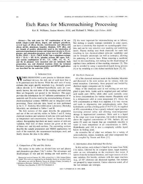
256 JOURNAL OF MICROELECTROMECHANICAL SYSTEMS, VOL. 5, NO. 4, DECEMBER 1996<br />
<strong>Etch</strong> <strong>Rates</strong> <strong>for</strong> <strong>Micromachining</strong> <strong>Processing</strong><br />
Kirt R. Williams, Student Member, IEEE, and Richard S. Muller, Life Fellow, IEEE<br />
Abstruct- The etch rates <strong>for</strong> 317 combinations of 16 materials<br />
(single-crystal silicon, doped, and undoped polysilicon,<br />
several types of silicon dioxide, stoichiometric and silicon-rich<br />
silicon nitride, aluminum, tungsten, titanium, TVW alloy, and<br />
two brands of positive photoresist) used in the fabrication of<br />
microelectromechanical systems and integrated circuits in 28 wet,<br />
plasma, and plasmaless-gas-phase etches (several HP solutions,<br />
H3P04, HNO3 H20 + N-F, KOH, Type A aluminum etchant,<br />
HZ 0 + HZ 0 2 + HF, H2 02, piranha, acetone, HF vapor, XeF2,<br />
and various combinations of SF6, CF4, CHF3, C12, 02, N2,<br />
and He in plasmas) were measured and are tabulated. <strong>Etch</strong><br />
preparation, use, and chemical reactions (from the technical<br />
literature) are given. Sample preparation and MEMS applications<br />
are described <strong>for</strong> the materials. [193]<br />
I. INTRODUCTION<br />
HEM DESIGNING a new process to fabricate microma&ined<br />
devices, the etch rate of each layer that is<br />
to be patterned must be known. While the etch rates of many<br />
etchants that target specific materials (e.g., thermally grown<br />
silicon dioxide in 5:l buffered hydrofluoric acid) are commonly<br />
known, the etch rates of the masking and underlying<br />
films are frequently not quoted in the literature. This paper<br />
provides this in<strong>for</strong>mation <strong>for</strong> 317 different combinations of 16<br />
materials and 28 etches used in the micromachining of microelectromechanical<br />
systems (MEMS) and in integrated-circuit<br />
processing. These etch-rate data, based on tests per<strong>for</strong>med<br />
in the U. C. Berkeley Microfabrication Laboratory (Berkeley<br />
Microlab), are tabulated in Tables I and 11.<br />
The first sections of this paper describe the preparation<br />
and use of the wet and dry etches in Tables I and 11, listing<br />
chemical reactions and variation of etch rate with such factors<br />
as temperature and concentration, based on literature on the<br />
subject. Recognizing that there are many sources of etch-rate<br />
variation, brief lists of these sources are given at the end<br />
of these wet- and dry-etch sections. The succeeding sections<br />
describe the sample preparation and MEMS applications <strong>for</strong><br />
each of the materials, the measurement techniques used, and<br />
finally discuss the data in the tables.<br />
11. ?kE WET ETCHES<br />
A. Comparison of Wet and Dry <strong>Etch</strong>es<br />
The etches in the tables are divided into wet and plasma<br />
and plasmaless-gas-phase (“dry”) etches. The advantages and<br />
disadvantages of wet and dry etching are well known 111,<br />
Manuscript received January 10, 1996; revised July 1, 1996. Subject Editor,<br />
K. Najafi. This work was supported by the Berkeley Sensor & Actuator Center.<br />
The authors are with the Berkeley Sensor & Actuator Center, University of<br />
Califomia at Berkeley, Berkeley, CA 94720-1770 USA.<br />
Publisher ltem Identifier S 1057-7157(96)08843-9.<br />
[2]; the most important <strong>for</strong> micromachining are as follows.<br />
Wet etching is usually isotropic (desirable in some cases),<br />
can have a selectivity that depends on crystallographic direction,<br />
and can be very selective over masking and underlying<br />
layers. Plasma etching uses fresh chemicals <strong>for</strong> each etch<br />
(resulting in less chemical-related etch-rate variability) and<br />
can be vertically anisotropic (as well as isotropic), allowing<br />
the patterning of narrow lines. When removing a sacrificial<br />
layer in micromachining, wet etching has the disadvantage of<br />
capillary-<strong>for</strong>ce pulldown of free-standing structures [3]. This<br />
can be avoided by using a supercritical-liquid drying process<br />
[4] or by switching to a dry-etched sacrificial layer [5],[61.<br />
B. Wet-<strong>Etch</strong> Chemicals<br />
All of the chemical mixtures made in the Berkeley Microlab<br />
and discussed in the next section are by volume, with one<br />
noted exception. Conversely, those prepared and bottled by<br />
chemical-supply companies are by weight.<br />
Many of the chemicals used in wet etching are not supplied<br />
in pure <strong>for</strong>m. Acetic acid is supplied pure and sulfuric<br />
acid nearly pure (96%), while other acids normally come<br />
in lower concentrations <strong>for</strong> various reasons. Phosphoric acid<br />
is a deliquescent solid at room temperature [7]. Above the<br />
85% concentration at which it is supplied, it is very viscous<br />
and tends to oligomerize into polyphosphoric acids. Pure<br />
hydrofluoric acid has a boiling point of 19.5”C [7]. As supplied<br />
at 49% concentration, it has a greatly r<strong>edu</strong>ced vapor pressure,<br />
increasing personal safety and allowing room-temperature<br />
storage in unpressurized containers. Nitric acid is a liquid<br />
in the range near room temperature, but tends to decompose<br />
above the supplied concentration of 70%. Sulfuric [8] and<br />
acetic [9] acids are liquids that are completely miscible in<br />
water at room temperature at all concentrations to 100%.<br />
Hydrofluoric acid [lo] is also a completely soluble liquid<br />
below its boiling point.<br />
An extensive list of other wet etchants <strong>for</strong> a variety of<br />
semiconductors, metals, insulators, and other compounds has<br />
been compiled by Vossen and Kern [ 111.<br />
C. In<strong>for</strong>mation about Individual Wet <strong>Etch</strong>es<br />
In this section, each etchant is listed by its name from Table<br />
I in italics, followed by its complete name, target material,<br />
notes on use, in<strong>for</strong>mation on the reaction(s) that occur, if<br />
known from the technical literature, and major sources of etchrate<br />
variation. For brevity, etchants with the same reactions<br />
(e.g., all HF solutions) are discussed together. The etchants<br />
are grouped by target material. Unless otherwise noted, all of<br />
the wet etchants are isotropic.<br />
1057-7157/96$05.00 0 1996 IEEE
WILLIAMS AND MULLER ETCH RATES FOR MICROMACHINING PROCESSING 257<br />
,<br />
__<br />
,<br />
a<br />
-<br />
a<br />
5<br />
-<br />
3<br />
3<br />
-<br />
a<br />
L<br />
-<br />
L<br />
!<br />
-<br />
0<br />
3<br />
L<br />
3<br />
8<br />
2<br />
.l 3 N d a C<br />
-4 0 0<br />
L<br />
3<br />
2<br />
3<br />
c<br />
9<br />
a s<br />
Y 0<br />
o 5<br />
3<br />
a<br />
-<br />
0<br />
, 0 a 0<br />
n<br />
__<br />
3<br />
a<br />
__<br />
0<br />
-<br />
e<br />
3<br />
-<br />
a N a<br />
a<br />
-<br />
3<br />
0<br />
0<br />
-<br />
0<br />
8<br />
Y<br />
-<br />
e<br />
8<br />
9<br />
-<br />
I<br />
'I<br />
4<br />
I<br />
9<br />
bS<br />
0<br />
It<br />
9<br />
;St
258 JOURNAL OF MICROELECTROMECHANICAL SYSTEMS, VOL. 5, NO. 4, DECEMBER 1996<br />
All wet etching was done at room temperature (about<br />
20" C in the temperature-controlled Berkeley Microlab), unless<br />
otherwise indicated. All wet etching was done with fresh<br />
solutions, agitating occasionally. To remove the vapors created<br />
by the etchants, all wet etching was done under fume hoods.<br />
1) Silicon Dioxide Wet <strong>Etch</strong>ants: Notes: All of the silicon<br />
dioxide etchants given here are based on hydrofluoric acid.<br />
HF-based etchants are used mainly <strong>for</strong> etching silicon dioxide,<br />
although they can also be used to remove silicon nitride. In<br />
our tests, they were observed to etch polysilicon very slowly,<br />
but other researchers have noted that various solutions attack<br />
polysilicon at the grain boundaries, resulting in noticeable<br />
surface roughness 1121, 1131. Recent research indicates that<br />
HF can diffuse through thin (
WILLIAMS AND MULLER ETCM RATES FOR MICROMACHINING PROCESSING 259<br />
Reaction: The literature does not list a chemical reaction<br />
<strong>for</strong> the etching of silicon nitride. Gelder and Hauser propose<br />
that the water in the solution hydrolizes the nitride to some<br />
<strong>for</strong>m of hydrous silica and ammonia [23].<br />
Gelder and Hauser [23] report the "real" activation energy<br />
<strong>for</strong> the etching of silicon nitride in a constant concentration of<br />
94.5% phosphoric acid as 0.99 eV. The "apparent" activation<br />
energies, taken with the etch temperature and boiling point<br />
being the same (i.e., <strong>for</strong> varying concentrations of HJPO~) are<br />
0.55 eV <strong>for</strong> silicon nitride, 1.20 eV <strong>for</strong> silicon dioxide, and<br />
1.15 eV <strong>for</strong> silicon. These apparent activation energies take<br />
into account the effects of temperature on both concentration<br />
of H3P04 in the solution and the etch reactions themselves.<br />
As the water content in the etch bath decreases (e.g., due to<br />
evaporation), the etch rate of silicon nitride decreases, while<br />
the etch rate of silicon dioxide increases [23], so the use of a<br />
reflux system is important in maintaining a constant etch rate<br />
and mask selectivity.<br />
3) Isotropic Silicon Wet <strong>Etch</strong>ant:<br />
Silicon etchant: Wet silicon etchant. This solution is<br />
mixed and bottled in the Berkeley Microlab from 126:60:5<br />
HN03 (70%) : H2O : NH4F (40%).<br />
Notes: This etch, similar to the HNO3 + H20 + HF etches<br />
discussed in a series of papers by Robbins and Schwartz [2],<br />
[24], is used mainly <strong>for</strong> polysilicon wet etching. The slight<br />
change in chemistry was used earlier at Trilogy [25]. It can<br />
be masked by photoresist.<br />
Reaction: A simplified description of the reaction is that<br />
the nitric acid in the solution oxidizes the silicon, then the<br />
hydrofluoric acid (<strong>for</strong>med from the fluoride ions in this acidic<br />
solution) etches the oxidized compound. Many metal etches<br />
not discussed in this paper also remove material in this twostep<br />
manner. The overall reaction is [2], [26]<br />
18HF + 4HN03 + 3% -+<br />
3H2SiFqa,) + 4NO(,) + 8Hz0.<br />
Turner has found the peak etch rate of silicon to occur at<br />
an HF:HNOs ratio of 4.5, the same ratio as in the balanced<br />
reaction given above [26]. The rate-limiting step <strong>for</strong> the etch<br />
solution in this table, which has a low HF concentration, is<br />
the supply of HF to the reaction site [26]. The etch rate of a<br />
given bath decreases with use as the HF is depleted. The use<br />
of NH4F rather than HF results in a buffer action, keeping the<br />
HF and HF; (both responsible <strong>for</strong> etching the oxidized silicon)<br />
concentrations from changing as rapidly with use [25]. Used<br />
solutions turn yellow due to dissolved NO gas.<br />
4) Orientation-Dependent Silicon Wet <strong>Etch</strong>ants:<br />
KOH 80 "C: Potassium hydroxide solution at 80 "C. Mixed<br />
from 1 kg KOH pellets : 2 liters HzO. This solution is<br />
about 29% KOH by weight because the KOH pellets normally<br />
contain 10 to 15% water [:27]. It is heated in a perfluoroalkoxy<br />
polytetrafluoroethylene (PFA) tank with recirculating pump.<br />
Notes: This solution is self heating. It should be allowed<br />
to equilibrate be<strong>for</strong>e using <strong>for</strong> a controlled temperature. When<br />
etching single-crystal silicon, the silicon can be masked with<br />
silicon nitride. To r<strong>edu</strong>ce undercutting of the nitride mask, a<br />
HF dip should be carried out immediately be<strong>for</strong>e the nitride<br />
deposition to remove any native oxide.<br />
We have found that the KOH in unagitated solutions tends<br />
to stratify, resulting in etch-rate variation from the top to the<br />
bottom of the solution. This problem was solved by the use<br />
of a recirculation pump.<br />
KOH is used <strong>for</strong> orientation-dependent etching (ODE) of<br />
single-crystal silicon. ODE'S attack ( 111)-type planes, which<br />
have a high bond density, much more slowly than other planes<br />
[2], [28]. (Un<strong>for</strong>tunately, this high-bond-density reasoning <strong>for</strong><br />
slow-etch-rate planes cannot be extended to explain the etchrate<br />
ratio between (100) and (110) planes [28].) The etch rate<br />
listed in Table I is the one perpendicular to the surface of the<br />
(100) wafers used <strong>for</strong> this etch-rate test. KOH stops etching<br />
on very heavily doped p-type material [29].<br />
Isopropyl alcohol is sometimes added to KOH solutions.<br />
This decreases the etch rate, but improves uni<strong>for</strong>mity, r<strong>edu</strong>cing<br />
the requirement <strong>for</strong> stirring [30]. It also slows (110)-plane and<br />
accelerates { 111)-plane etching (not affecting {loo) planes<br />
much) and lessens the severity of the etching of convex corners<br />
[281.<br />
(Other inorganic hydroxides [29], [30], organic hydroxides<br />
such as tetramethyl ammonium hydroxide (TMAH) [31], [33],<br />
and ethylenediamine pyrocatechol (EDP) [29], [30], an organic<br />
base, are orientation-dependent etchants similar to KOH. In the<br />
Berkeley Microlab and others, EDP has been found to be better<br />
than KOH at stopping abruptly at heavily boron-doped regions<br />
[29], [32]. TMAH has the advantages of not being a source of<br />
sodium (which contaminates the gate oxide in MOS circuitry)<br />
and not attacking aluminum when it has been "doped" with a<br />
small amount of silicon [33].)<br />
Reaction: Several different reactions <strong>for</strong> KOH etching of<br />
silicon are listed in the literature [2], [30]. Seidel et al. list the<br />
gross reaction as [30]<br />
Si + 2 OH- + 2 H2O + SiOz(OH)&- + 2Hzp).<br />
Glembocki et al. list a very similar reaction [34]. This chemical<br />
reaction is independent of the source of the hydroxide ion,<br />
whether LiOH, NaOH, or KOH, in agreement with experiment.<br />
The dependence of the reaction on p-type doping is explained<br />
by Seidel et al. [30] and also by Raley et al. [32]:<br />
At intermediate steps in the etch, four free electrons are<br />
generated that reside near the surface be<strong>for</strong>e being exchanged.<br />
P-type doping r<strong>edu</strong>ces this surface supply of electrons. The<br />
etch rate decreases as the fourth power of the concentration<br />
<strong>for</strong> p-type doping beyond degeneracy, which occurs at about<br />
2 x 10¹⁹ cmP3 active boron atoms.<br />
Seidel found the etch-rate ratio <strong>for</strong> (110) to (100) to (111)<br />
planes to be about 160:lOO:l at 20 "C, decreasing to 50:30:1 at<br />
100 "C [30]. In contrast, Kendall measured even higher ratios<br />
of 400:200:1 at 85 "C and discussed the extreme difficulty in<br />
making these measurements [28].<br />
The etch rate in KOH increases with temperature. Seidel<br />
et al. give activation energies <strong>for</strong> the concentration of KOH<br />
in Table I (29% by weight) of 0.59 eV <strong>for</strong> (100) silicon and<br />
0.84 eV <strong>for</strong> silicon dioxide [30]. They also found that, at 80<br />
"C, the etch rates of (100) silicon and silicon dioxide peak<br />
at concentrations of about 18 and 34 weight %, respectively.<br />
Lower concentrations of either Hz0 or OH-, both used in the<br />
reaction, result in lower etch rates. The surfaces, however,
260 JOURNAL OF MICROELECTROMECHANICAL SYSTEMS, VOL. 5, NO. 4, DECEMBER 1996<br />
appear rough and insoluble white residues <strong>for</strong>m <strong>for</strong> KOH (Another tungsten etch, which has been found in our lab not<br />
concentrations below 20% 1351. The temperature and KOH to leave the residue mentioned above, contains 1 liter H20,<br />
concentration effects on the etch rate (ER) of (100) silicon 34 g K3Fe(CN),, 13.4 g KOH, and 33 g KH2PO4. It can be<br />
were empirically found to fit well to the equation [30] patterned with photoresist, does not attack oxide or nitride at<br />
an appreciable rate, and etches tungsten at 340 kmin).<br />
ERsi in KOH = ~ J[H~O]~[KOH]'.*~-~~'~~<br />
where the etch rate is in pmh, the concentrations are in<br />
mol/liter, k0 = 2480 pm/hr.(m~l/liter)-~.~~, and EA = 0.595<br />
eV.<br />
5) Metal Wet <strong>Etch</strong>ants:<br />
Aluminum <strong>Etch</strong>ant Type A: Aluminum etchant Type A at<br />
50 "C. This solution, sold commercially, is composed of 80%<br />
phosphoric acid, 5% nitric acid, 5% acetic acid, and 10% water<br />
[36j. Some <strong>for</strong>mulations may include a surfactant. According<br />
to the manufacturer, this etchant is designed to etch aluminum<br />
at 6000 kmin at 50 OC. It is heated in a PFA tank.<br />
Notes: This etch is used <strong>for</strong> wet etching of aluminum. It<br />
can be masked with photoresist.<br />
Reaction: In this multistep etch [37], the aluminum is first<br />
oxidized by the nitric acid. The phosphoric acid and water simultaneously<br />
etch the resulting oxide. With the concentrations<br />
given, these two processes occur at roughly the same rate, so<br />
that either could be the rate-limiting step [37]. Because the<br />
phosphoric acid also removes the native aluminum oxide, no<br />
additional component is needed <strong>for</strong> this purpose.<br />
The etch rate increases with temperature and decreases<br />
significantly with use due to depletion of the active chemicals.<br />
Similar solutions with a r<strong>edu</strong>ced fraction of water etch more<br />
rapidly [37j. Agitating aids etch-rate uni<strong>for</strong>mity across a wafer,<br />
as well as helping to remove the hydrogen bubbles that evolve.<br />
If not removed, these bubbles can block the flow of reactant<br />
to the surface, resulting in localized etch nonuni<strong>for</strong>mity.<br />
Titanium <strong>Etch</strong>ant: Mixed from 20:1:1 HzO : HF (49%)<br />
: H202 (30%).<br />
Notes: HF is the active ingredient is this etchant, so it<br />
also etches oxides. Raising the fraction of HF in the solution<br />
increases the etch rate. Titanium etched in this solution can be<br />
masked with photoresist.<br />
Reaction: No reaction is given in the literature. Titanium<br />
is known to be readily oxidized, so it likely <strong>for</strong>ms an oxide<br />
from the water and peroxide, which is readily etched by the<br />
HF in this solution.<br />
H202 (30%): Hydrogen peroxide (30% by weight). Produced<br />
commercially.<br />
Notes: This etchant is used to wet-etch tungsten and its alloys,<br />
which can be masked with photoresist. We have observed<br />
that Hz02-etching of tungsten sometimes leaves a residue.<br />
Reaction: In this etch, a film of tungsten oxide is <strong>for</strong>med<br />
that is dissolved in the hydrogen peroxide [38]. This etchant<br />
also etches tungstedtitanium alloys, but not pure titanium.<br />
The etch rate rises with temperature, but any significant<br />
increase may cause a photoresist mask to be eroded or to<br />
peel. CVD silicon-based masking layers, successful <strong>for</strong> other<br />
films, cannot be used with tungsten, as the silicon reacts to<br />
<strong>for</strong>m tungsten silicides during the high-temperature deposition.<br />
Sputtered aluminum is a suitable mask layer, although when<br />
used, it becomes difficult to observe the end of the aluminum<br />
etch either optically or electrically.<br />
6) Wet Wafer Cleaning:<br />
Piranha 120°C: Piranha in 120 "C heated bath. In the<br />
Berkeley Microlab, piranha consists of about 5.6 liters of 96%<br />
H2S04 heated to 120 "C in a PFA tank, to which 100 ml of<br />
30% H2Oz is added immediately be<strong>for</strong>e each use.<br />
Notes: Piranha has been in use <strong>for</strong> wafer cleaning <strong>for</strong><br />
decades [l], [39], [40]. The term refers to a hot solution of<br />
HzSO4 and HzOz mixed in any ratio [39], [40]. In lower<br />
ratios of HzSO4 to HzO2 (e.g., 5:1), the solution is noticeably<br />
self-heating (no external heat source is needed).<br />
Piranha is used in the Berkeley Microlab <strong>for</strong> 10 min to<br />
clean organic and metallic contaminants from wafers be<strong>for</strong>e<br />
furnace steps. Kern and hotinen [41] have observed that the<br />
desorption of 90% of monatomic metal films from silicon into<br />
similar acidic peroxide solutions can take several minutes.<br />
Reaction: Like other acidic hydrogen peroxide solutions,<br />
piranha strips photoresist and other organics by oxidizing<br />
them, and removes metals by <strong>for</strong>ming complexes that stay<br />
in the solution [41], [42]. It does not affect silicon dioxide<br />
and silicon nitride and has the minor effect on bare silicon of<br />
<strong>for</strong>ming a thin layer of hydrous silicon oxide [41]. This oxide<br />
film is typically removed with a short (10-s) 1O:l or 25:l HF<br />
dip after the piranha clean and rinse.<br />
Acetone: Acetone spray from a photoresist developing<br />
machine.<br />
Notes: Acetone is used to strip photoresist (PR) and <strong>for</strong><br />
lift-off patterning of films [l], [2]. The machine used in the<br />
Berkeley Microlab gives a stream of fresh acetone <strong>for</strong> PR<br />
stripping.<br />
An acetone bath would be used <strong>for</strong> liftoff processes [ 11, [2].<br />
Lift-off processes can be sped up by heating the acetone (with<br />
a loose lid to slow evaporative loss) or by placing it in an<br />
ultrasonic tank.<br />
While acetone readily stripped the photoresists listed in this<br />
table, its effectiveness depends on the processing the PR has<br />
gone through. Heating the PR by a few tens of degrees above<br />
120 "C, either while hardbaking or during a process step,<br />
will make it significantly harder to dissolve [ 11. Some plasma<br />
processing gives rise to a similar effect (known as "plasma<br />
hardening"). In such cases, an oxygen plasma, a commercial<br />
PR stripper (such as Baker PRS-2000), or piranha can usually<br />
be used to remove the PR.<br />
Reaction: Acetone breaks down the structure of the photoresist,<br />
making it soluble [l].<br />
D. Wet-<strong>Etch</strong>-Rate Variation<br />
The wet-etch rates given in Table I can vary <strong>for</strong> reasons<br />
that are usefully divided into three groups: the etch setup,<br />
the material being etched, and the layout and structure on<br />
the substrate. The most significant effects on the wet-etch<br />
rate in each of these categories are as follows (due to space<br />
constraints, the reader is referred to the references <strong>for</strong> detailed<br />
in<strong>for</strong>mation on these sources of etch-rate variation).
WILLIAMS AND MULLER ETCH RATES FOR MICROMACHINING PROCESSING 261<br />
<strong>Etch</strong>-rate variation due to the etch setup is a function of 1)<br />
temperature [43]; 2) loss of reactive species [43]; 3) loss of<br />
liquids to evaporation [30], [44]; 4) mixing; 5) stratification<br />
of the solution; 6) etch-product blocking of chemical flow [2];<br />
7) elapsed time from the start of the etch; 8) applied potential<br />
[2], [4], [5]; 9) illumination [45]; and IO) contamination. <strong>Etch</strong>rate<br />
variation due to the material being etched is affected by<br />
11) impurities in or on the material being etched [20], [46];<br />
12) microstructure [15], [47], [48]; and 13) film stress [49],<br />
[50]. <strong>Etch</strong>-rate variation due the layout and structure on the<br />
substrate is affected by 14) the distribution and fraction of<br />
surface area of the exposed target layer (loading) [2], [15],<br />
and 15) the structure geometry [13].<br />
111. THE PLASMA AND PLASMAL,ESS-GAS-PHASE ETCHES<br />
A. Purposes of the <strong>Etch</strong> Gases<br />
Because many gases are used in more than one of the etches<br />
in Table 11, each gas (in italics) and its purpose are presented<br />
here.<br />
I) Oxygen (02): dissociates into 0 radicals, which are more<br />
reactive. Oxygen has several purposes. Pure 0 2 plasmas are<br />
used to etch photoresist. In plasmas involving CF4, 0 atoms<br />
displace F in the CF4 molecule, generating more free F [51].<br />
This can both increase the etch rate and cause enough F to be<br />
present to allow the <strong>for</strong>mation of C-F sidewall polymer films.<br />
2) Sulfur Hexafluoride (SF6): SF6 is one source of very<br />
reactive F atoms that etch all of the materials in Table I1 except<br />
<strong>for</strong> aluminum. Fluorine atoms are not very selective, etching<br />
most of these materials at rates varying by less than a factor<br />
of 5. Molecular fluorine (F2) is not used <strong>for</strong> silicon etching<br />
because it is hazardous, and, <strong>for</strong> reasons not understood, it<br />
leaves rough surfaces [Ill, [52].<br />
3) TetraJluoromethane (CF4, carbon tetrafluoride, Freon<br />
14): CF4 is a source of F and also a source of C, both of<br />
which are required <strong>for</strong> C-F sidewall-polymer <strong>for</strong>mation.<br />
4) Trzyuoromethane (CHF3, Freon 23): CHFs is another<br />
source of F and C, but with a lower ratio of F to C.<br />
5) Chlorine (C12): C12 dissociates into C1 atoms, which are<br />
quite reactive. Like F, C1 etches most materials, including<br />
aluminum.<br />
6) Trichloromethane (CHCl3, chloro<strong>for</strong>m): CHC13 supplies<br />
chlorine <strong>for</strong> etching and carbon and chlorine <strong>for</strong> sidewall<br />
polymer <strong>for</strong>mation [521.<br />
7) Boron Trichloride (BC13): BC13 etches the native aluminum<br />
oxide film on aluminum. It also scavenges 02 and<br />
HzO in the vacuum system, preventing oxide growth [53].<br />
8) Helium (He): He can be used in plasma etching as a<br />
diluent and a plasma stabilizer [51]. Diluents give the user<br />
another process control variable. For example, an inert gas can<br />
be added to increase the total pressure while keeping the partial<br />
pressures of the other gases constant. In addition, some gas<br />
species can improve energy transfer from the “hot” electrons<br />
to reactive gas molecules (e.g., He enhances the dissociation<br />
of BC13 [51]).<br />
9) Nitrogen (Nz): N2 is also used as a diluent.<br />
10) Hydrogen fluoride vapor (HF): HF vapor evaporates<br />
rapidly from concentrated HF solutions. Like its liquid counterpart,<br />
it can be used <strong>for</strong> etching silicon oxides.<br />
11) Xenon DiJluoride (XeF2): XeF2 is supplied as granular<br />
crystals. At room temperature, it has an equilibrium vapor<br />
pressure of about 4.5 Torr [54]. XeF2 supplies fluorine atoms<br />
in the plasmaless-gas-phase etching of silicon and some other<br />
materials.<br />
12) Other Gases: Many other gases in various combinations<br />
have been used <strong>for</strong> plasma etching, as discussed in several of<br />
the references [l], [2], [51]-[53].<br />
B. In<strong>for</strong>mation About Individual Plasma and<br />
Plasmaless Gas-Phase <strong>Etch</strong>es<br />
All of the plasma etches in Table I1 were done with recently<br />
cleaned chambers. The plasma etches are fairly anisotropic<br />
unless otherwise noted. The anisotropic plasma etches presented<br />
in this section have recipes that are based on the<br />
manufacturers’ general recommendations <strong>for</strong> each machine,<br />
adapted to yield a useful compromise among a reasonably fast<br />
etch rate <strong>for</strong> the target material, fairly straight sidewalls, and<br />
selectivity over a photoresist mask layer.<br />
In this section, the etches are grouped by reactive plasma<br />
species and target material. The reactions listed are summaries;<br />
the occurrence of a complicated series of subreactions, adsorptions,<br />
and possibly energetic ion involvement should be<br />
considered typical. Details of some of the reactions are given<br />
in the references.<br />
Each etch is listed by its name from Table I1 in italics,<br />
which includes the gases, their flow rates, equipment brand and<br />
model number, power, pressure, electrode gap, and operating<br />
frequency.<br />
The plasmaless-gas-phase etchants, HF vapor and XeF2, are<br />
listed with the plasma etches because they are more similar<br />
to chemical-plasma etching than to wet etching: reactant and<br />
product flow occurs in the gas phase and there is a fresh flow<br />
of reactants to the etch surface.<br />
I) Fluorocarbon-Plasma Silicon-Dioxide <strong>Etch</strong>es: Reaction:<br />
It appears that CF, (x 5 3) radicals chemisorb on the Si02<br />
and dissociate. The radicals supply carbon to <strong>for</strong>m CO, C02,<br />
and COF2 gases from the oxygen in the film. They also supply<br />
fluorine to <strong>for</strong>m SiF4 gas [55]. Overall reactions such as the<br />
following occur [2]:<br />
3SiO2 + 4CF3 -+ 2C0 + 2C02 + 3SiF4<br />
Si02 + 2CHF2 -+ 2C0 + H2 + SiF4.<br />
CF4+ CHF3+ He (90:30:130 sccm), Lam 590, 450 W,<br />
2.8 T, gap = 0.38 em, 13.56 MHz: Parallel-plate configuration,<br />
graphite electrode (others are aluminum), driven electrode area<br />
M<br />
350 cm2.<br />
Notes: This etch targets silicon dioxide, but also etches<br />
silicon nitride well. It can be patterned with photoresist (PR).<br />
This etch is anisotropic (fairly vertical sidewalls).<br />
If total etch times longer than about 2 min are required, the<br />
etch is often broken up into several shorter times, giving the<br />
photoresist a chance to cool and thus erode less.
262 JOURNAL OF MICROELECTROMECHANICAL SYSTEMS, VOL. 5, NO. 4, DECEMBER 1996<br />
I<br />
L<br />
I
WILLIAMS AND MULLER ETCH RATES FOR MICROMACHINING PROCESSING 263<br />
CF4+ CHF3+ He (90:30:130 sccm), Lam 590, 850 W,<br />
2.8 T, gap = 0.38 em, 13.56MHz: Parallel-plate configuration,<br />
graphite electrode (others are aluminum), driven electrode area<br />
x 350 cm2.<br />
Notes: This is a faster oxide etch than the lower-power etch<br />
above, but with lower selectivity to photoresist.<br />
2) Fluorine-Atom-Plasma Silicon-Nitride <strong>Etch</strong>es:<br />
Reaction: Fluorine atoms are adsorbed onto the surface<br />
one at a time. in a surface reaction, volatile products are<br />
<strong>for</strong>med. The overall reaction is 121<br />
Si3N4 + 12F + 3SiF4 + 2N2.<br />
The apparent activation energy <strong>for</strong> F-atom etching of Si3N4<br />
is about 0.17 eV 1531.<br />
SF6+ He (13:21 sccm), Technics PE II-A, 100 W, 250 mT,<br />
50 kHz sq. wave: Parallel-plate configuration, fixed gap x 2.6<br />
cm, driven electrode area x 600 cm2. The chamber holds four<br />
wafers; the test was per<strong>for</strong>med with one wafer.<br />
Notes: This etch is used to plasma-etch silicon nitride. it<br />
can be masked with photoresist.<br />
This etch exhibits a severe loading effect. It is not only<br />
affected by the number of wafers in the chamber, but also by<br />
the fraction of nitride surface area that is exposed. Furthermore,<br />
the etch rate varies with position in the chamber, so<br />
wafers should be rotated three or four times during an etch<br />
<strong>for</strong> uni<strong>for</strong>mity.<br />
Plasma etching, especially at higher power, heats the chmber,<br />
which can affect etch rates and thus selectivity. During<br />
all Technics PE 11-A tests, the plate temperature varied from<br />
20 to 30°C.<br />
CF4+ CHF3+ He (I0:5:10 sccm), Technics PE II-A, 200<br />
W, 250 mT, 50 kHz sq. wave: Parallel-plate configuration,<br />
fixed gap x 2.6 cm, driven electrode area x 600 cm2. The<br />
chamber holds four wafers; the test was per<strong>for</strong>med with one<br />
wafer.<br />
Notes: This silicon nitride plasma etch uses fluorocarbons<br />
rather than SFs as the source of F atoms.<br />
SFs+ He (175:50 sccm), Lam 480, 150 W, 375 mT, gap<br />
= 1.35 cm, 13.56 MHz: Parallel-plate configuration, driven<br />
electrode area x 350 cm2.<br />
This silicon nitride plasma etch is in a single-wafer system.<br />
The slower etch rate than the etch listed below is intended<br />
<strong>for</strong> thin nitride films. It can be patterned with photoresist. The<br />
etch is anisotropic (fairly vertical sidewalls).<br />
SFsf He (175:50 sccm), Lam 480, 250 W, 375 mT, gap<br />
= 1.35 em, 13.56 MHz: Parallel-plate configuration, driven<br />
electrode area M 350 cm2.<br />
Notes: This silicon nitride plasma etch is faster and there<strong>for</strong>e<br />
useful <strong>for</strong> thicker nitride films. It can be patterned with<br />
photoresist.<br />
If total etch times longer than about 2 min are required, the<br />
etch is often broken up into several shorter times, giving the<br />
PR a chance to cool and thus erode less.<br />
SF6 (25 sccm), Tegal Inline Plasma 701, 125 W, 200 mT,<br />
13.56 MHz: Parallel-plate configuration, fixed gap x 3.8 cm,<br />
driven electrode area x 250 cm2.<br />
Notes: This slower etch is intended <strong>for</strong> thinner, stoichiometric<br />
silicon nitride films.<br />
CF4+ CHF3+ He (45:15:60 sccm), Tegal Inline Plasma<br />
701, 100 W, 300 mT, 13.56 MHz: Parallel-plate configuration,<br />
fixed gap x 3.8 cm, driven electrode area x 250 cm2.<br />
Notes: This etch has a different gas chemistry than the<br />
previous etch, aimed at thicker, silicon-rich nitride films.<br />
3) Plasma Silicon <strong>Etch</strong>es:<br />
Clz+ He (180:400 sccm), Lam Rainbow 4420, 275 W,<br />
425 mT, 40 "C, gap = 0.80 cm, 13.56 MHz: Parallel-plate<br />
configuration, driven electrode area sz 390 cm2.<br />
Notes: This is an anisotropic silicon plasma etch. An SF6<br />
step prior to this one is typically used to break through the<br />
native oxide.<br />
This etch has been used to micromachine 80-pm-deep<br />
trenches with fairly vertical sidewalls [56].<br />
Reaction: Chlorine atoms are chemisorbed one at a time<br />
on the silicon surface, eventually <strong>for</strong>ming volatile Sic14 [53].<br />
The overall reaction is<br />
4Cl-t Si + SiCL.<br />
Chlorine etching of undoped silicon occurs very slowly in<br />
the absence of ion bombardment [53]. Unlike F-atom silicon<br />
etches, C1- and Br-based etches tend to be vertical 1511.<br />
As the Fermi level rises, the energy barrier <strong>for</strong> charge<br />
transfer of chemisorbed C1, a step in the etch process, falls<br />
[53]. Thus, p-type doping slows etching while n-type doping<br />
accelerates it.<br />
Chlorine-based plasma etch rates of single-crystal silicon<br />
can also depend on crystallographic orientation. Kinoshita and<br />
Jinno found that, with CC14 + He plasmas, the (100) and<br />
(110) planes could be etched faster than the (111) planes<br />
[57]. The selectivity was not, however, as great as with KOHor<br />
EDP-based etches.<br />
HBr + C12 (70:70 sccm), Lam Rainbow 4420, 200 W,<br />
300 mT, 40"C, gap = 0.80 cm, 13.56 MHz: Parallel-plate<br />
configuration, driven electrode area x 390 cm2.<br />
Notes: This is another anisotropic silicon plasma etch, with<br />
better selectivity of silicon over oxide.<br />
Reaction: Bromine atoms probably react with silicon in a<br />
manner similar to chlorine as described above.<br />
4) Plasma Metal <strong>Etch</strong>es:<br />
Cl2 + BC13 + CHCl3 + N2 (30:50:20:50 sccm), Lam 690,<br />
250 W, 250 mT, 60 "C, 13.56 MHz: Parallel-plate groundedchuck<br />
configuration, fixed gap x 2.5 cm, driven electrode area<br />
x 350 cm2.<br />
Notes: This is an anisotropic aluminum plasma etch due to<br />
the sidewall inhibitor <strong>for</strong>med from the CHC13 [52].<br />
Due to poor selectivity, <strong>for</strong> thick layers of Al, thicker<br />
photoresist, plasma-hardened PR, or a more-durable masking<br />
layer must be used. The higher temperature is used to keep the<br />
etch product volatile so that it leaves the wafer [2] and does<br />
not coat the chamber or exhaust plumbing.<br />
Reaction: The dominant overall reaction below 200 "C [52]<br />
is<br />
2A1+ 3C12 + A12Cls.<br />
Cl2 rather than C1 appears to be the main etchant [52]. The<br />
etch product becomes AlC13 at higher temperatures [lll, [521.
264 JOURNAL OF MICROELECTROMECHANICAL SYSTEMS, VOL. 5, NO. 4, DECEMBER 1996<br />
All aluminum etches in the Berkeley Microlab are followed<br />
by airlock plasma processing: CF4 = 90 sccm, 0 2 = 10 sccm,<br />
P = 400 W, <strong>for</strong> 1 min. The airlock recipe is not intended to<br />
do any etching. It replaces the chlorine in the residual AlzC16<br />
with fluorine. If this step were not per<strong>for</strong>med, the chlorine<br />
would <strong>for</strong>m hydrochloric acid upon exposure to atmospheric<br />
moisture, causing later corrosion of the aluminum.<br />
SF6 (80 sccm), Tegal Inline Plasma 701, 200 W, 150 mT,<br />
40 “C, 13.56 MHz: Parallel-plate configuration, fixed gap M<br />
3.8 cm, driven electrode area M 250 cm2. Grounded chuck.<br />
Notes: This tungsten plasma etch is fairly isotropic. CF4<br />
added to the feed gas increases anisotropy as sidewall polymers<br />
<strong>for</strong>m, but slows the etch rate.<br />
The chuck is heated to enhance the etch rate.<br />
Reaction: The overall reaction is<br />
W + 6F --+ WF6.<br />
5) Oxygen-Plasma Photoresist <strong>Etch</strong>es: Reaction: Oxygen<br />
atoms “bum” or “ash” (a misnomer) the organic photoresist,<br />
<strong>for</strong>ming mostly HzO,CO2, and CO [53]. Activation energies<br />
<strong>for</strong> 0-atom etching of photoresist have been measured in the<br />
range of 0.22 to 0.65 eV [53]. Below 60 OC, PMMA has an<br />
activation energy of about 0.2 eV [521.<br />
02 (51 sccm), Technics PE 11-A, 50 W, 300 mT, 50 kHz<br />
sq. wave: Parallel-plate configuration, gap M 2.6 cm, driven<br />
electrode area = 600 cm2. The chamber holds four wafers;<br />
the test was per<strong>for</strong>med with one wafer.<br />
Notes: This plasma-processing step is used <strong>for</strong> “descumming”<br />
(removing undesired thin layers) of freshly developed<br />
photoresist, typically <strong>for</strong> one minute. Unbaked OCG 820 PR<br />
was removed 6% faster than hardbaked PR during a descum<br />
test.<br />
02 (51 sccm), Technics PE II-A, 400 W, 300 mT, 50 kHz<br />
sq. wave: Parallel-plate configuration, fixed gap w 2.6 cm,<br />
driven electrode area M 600 cm2. The chamber holds four<br />
wafers; the test was per<strong>for</strong>med with one wafer.<br />
Notes: This oxygen plasma is used to ash (strip) photoresist<br />
<strong>for</strong> 5-10 min. A power of 300 W is also often used. It has<br />
been argued that lower power is better because there is less<br />
possibility of plasma hardening during stripping and of damage<br />
to MOS devices.<br />
A loading effect, in which the etch rate decreases when there<br />
is more photoresist surface area, has been observed. In a 400<br />
W PR stripping test, ashing four wafers at the same time was<br />
23% slower than ashing one alone.<br />
6) Plasmless HF-Vapor Silicon-Dioxide <strong>Etch</strong>:<br />
HF Vapor, 1 cm over plastic dish, Room temperature<br />
and pressure: Notes: Like liquid-based HF etches, HF vapor<br />
etches silicon dioxide. It has been used to remove native oxide<br />
from silicon be<strong>for</strong>e the growth of epitaxial silicon [58] and<br />
other processes such as the XeF2 etching of silicon.<br />
In these tests, the HF/HzO vapor condensed into droplets<br />
on the surfaces of the oxide samples during the 1-min etch,<br />
causing faster etching where these droplets had <strong>for</strong>med. This<br />
nonuni<strong>for</strong>m etching can be greatly r<strong>edu</strong>ced by etching in<br />
“pulses,” removing the wafer from the vapor be<strong>for</strong>e droplets<br />
<strong>for</strong>m and allowing it to evaporate.<br />
HF vapor may also be suitable <strong>for</strong> vapor-phase removal<br />
of a sacrificial oxide layer <strong>for</strong> micromechanical fabrication;<br />
however, caution should be used with photoresist masks,<br />
which may peel (in these tests, the photoresist peeled when<br />
the wafers were rinsed).<br />
In these tests, thermal oxide was etched at one third the<br />
rate of unannealed PSG. Other researchers have found that<br />
this selectivity goes up by two orders of magnitude when the<br />
wafers are heated to 50 “C [59].<br />
Reaction: The overall reaction is [58]<br />
Si02 + 4HF + SiF4 + HzO.<br />
Water is assumed to catalyze the reaction [%I, so a pure HF<br />
vapor may have a much slower etch rate than that over the<br />
49% HF/51% HzO used here. There is a brief incubation time<br />
at the beginning of the etch during which water molecules<br />
condense on the surface to be etched [58].<br />
7) Plasmaless XeFz Silicon <strong>Etch</strong><br />
XeFz, Simple custom vacuum chamber, room temperature,<br />
2.6 Torr: Notes: XeF2 was first synthesized in 1962 [60] and<br />
has been the subject of several papers on silicon etching [54],<br />
[61], but was only recently “rediscovered” <strong>for</strong> its suitability<br />
<strong>for</strong> micromachining [62].<br />
XeFz gas has the unusual capability to etch silicon at a<br />
significant rate without requiring a plasma to generate reactive<br />
species. As with chemical-plasma etching [52], etching is<br />
isotropic. The etched surface in deeply etched bulk silicon has<br />
been reported to have a roughness of several micrometers [62].<br />
XeFz has been used to micromachine free-standing structures<br />
made of aluminum and polysilicon protected by a layer of<br />
oxide [62]. XeF2 has the advantage over wet silicon etchants<br />
of gently etching without applying capillary <strong>for</strong>ces, and the<br />
advantage over plasma etches of being extremely selective<br />
over almost all of the traditional masking layers, such as silicon<br />
dioxide, some silicon nitrides, and photoresist.<br />
Because the native oxide on silicon surfaces completely<br />
stops etching, the silicon etch samples in these etch-rate tests<br />
were dipped in 1O:l HF, rinsed, and spun dry a few minutes<br />
be<strong>for</strong>e the etch rate tests. A period of 18 h in a wafer box<br />
in room air was found to be sufficient to grow enough native<br />
oxide on doped polysilicon to stop etching completely.<br />
The etch rate has been reported to be extremely loaddependent<br />
[62], and measured values in our lab are as low<br />
as 11 ndmin (<strong>for</strong> some regions of the wafer) when an entire<br />
4-in. wafer is exposed to the XeF2, up to 10 pdmin <strong>for</strong> small<br />
chips of silicon.<br />
The etching apparatus used <strong>for</strong> these etch-rate measurements<br />
allowed exposure of a 4-in. wafer to a 3.5-liter volume of<br />
XeF2 at its room-temperature equilibrium pressure <strong>for</strong> 30 s,<br />
after which the etch chamber was pumped down <strong>for</strong> 30 s. For<br />
etches of total time longer than 30 s (all data here are <strong>for</strong> one<br />
minute of etch time), this “pulsed-etching’’ cycle was repeated.<br />
Reaction: XeFz molecules are physisorbed on the silicon<br />
surface [61] and dissociate to release volatile xenon atoms,<br />
while the fluorine atoms (not Fz [54]) remain to react with the<br />
silicon to <strong>for</strong>m volatile SiF4. The overall reaction is<br />
2XeF2 + Si + 2Xe + SiF4.
WILLIAMS AND MULLER ETCH RATES FOR MICROMACHINING PROCESSING 265<br />
The limiting step in the etching process appears to be the<br />
supply of fluorine atoms to the reaction site. Different steps<br />
in the supply processes dominate at different temperatures,<br />
causing a minimum in the etch rate of silicon as a function of<br />
temperature at around 410 K 1611. Ibotson et al. hypothesize<br />
that the etch rate increases below 410 K because the surface<br />
coverage of physisorbed XeF2 is greater (the XeF2 is less<br />
volatile), and this is the etch-rate-limiting step. When the<br />
etch-rate data at these lower temperatures were fitted to an<br />
Arrhenius equation multiplied by the density of XeF2, the<br />
effective activation energy was found to be negative at -0.14<br />
eV (which corresponds to a positive activation energy <strong>for</strong><br />
desorption). Above 410K the surface coverage is lower, but<br />
direct impact dissociation greatly increases the supply of<br />
fluorine atoms <strong>for</strong> the reaction. The effective activation energy<br />
<strong>for</strong> these higher temperatures was found to be 0.26 eV.<br />
The etch rate of silicon has been observed to be proportional<br />
to the density of XeF2 molecules <strong>for</strong> pressures below 0.5 Torr,<br />
rising less than linearly at higher pressures [61]. The etch rate<br />
has been found to be proportional to the incident flux of XeF2<br />
under flow that is <strong>for</strong>ce-blown perpendicular to the surface.<br />
While according to several references, XeF2 alone does not<br />
etch silicon dioxide and nitride (to the contrary, stoichiometric<br />
silicon nitride was etched slowly in our tests), it does etch these<br />
dielectrics in the presence of ion or electron bombardment and<br />
under UV radiation [54]. This may help to explain why fluorine<br />
atoms are nonselective in plasma etches.<br />
C. Plasma-<strong>Etch</strong>-Rate Variation<br />
Assuming that an etch chemistry (reactive gases and additives),<br />
reactor configuration (grounded or driven wafer holder),<br />
and RF-power supply (which sets the frequency and power<br />
range) have been selected, we have identified a number of<br />
factors that can affect plasma-etch rates. These sources of etchrate<br />
variation can be divided into three categories: the etch<br />
setup, the material being etched, and the layout and structure<br />
on the substrate. The most significant effects on plasma-etch<br />
rate in each category are as follows (due to space constraints,<br />
the reader is referred to the references <strong>for</strong> detailed in<strong>for</strong>mation<br />
on these sources of etch-rate variation).<br />
<strong>Etch</strong>-rate variation due to the etch setup is a function of 1)<br />
power [52]; 2) pressure [52], [63]; 3) gas-flow rates [53]; 4)<br />
temperature [52], [53]; 5) film blocking of chemical flow [I],<br />
[64]; 6) elapsed time from the start of the etch; 7) materials<br />
present in the plasma chamber [2]; 8) changes in the etch<br />
chamber (e.g., wear of the electrode); and 9) contamination.<br />
<strong>Etch</strong>-rate variation due to the material being etched is affected<br />
by 10) impurities in or on the material being etched [53]; 11)<br />
microstructure; and 12) film stress. <strong>Etch</strong> rates also vary as a<br />
consequence of the layout and structure due to the 13) distribution<br />
and fraction of surface area of the target layer exposed<br />
(loading effect) [15]; and 14) specimen structure geometry.<br />
IV. SAMPLE PREPARATIONMEMS APPLICATIONS<br />
Most of the materials listed in the etch-rate tables are<br />
frequently used in the U. C. Berkeley Microfabrication Laboratory<br />
<strong>for</strong> micromachining and IC fabrication. The materials are<br />
discussed in the following list, which shows the abbreviated<br />
material names from Tables I and I1 in italics. The refractive<br />
index (RI) of each transparent film, used in thickness measurements,<br />
is listed. Preparation methods <strong>for</strong> the films are given,<br />
along with some MEMS applications and comments.<br />
SC Si (100): Single-crystal silicon, lightly doped with<br />
boron, with (100) orientation.<br />
Single-crystal silicon, in the <strong>for</strong>m of wafers, is the standard<br />
starting material <strong>for</strong> bulk micromachining [65].<br />
Poly n+: In-situ heavily n-doped polycrystalline silicon.<br />
RI = 3.97.<br />
Deposited on a wafer with thermal oxide already on it to<br />
enable interferometric thickness measurements. Deposited in<br />
a Tylan LPCVD furnace with the recipe SiH4 = 120 sccm,<br />
PH3 = 1 sccm, 605 "C,p = 300 mT. No anneal.<br />
This deposition temperature and pressure were chosen to<br />
yield a low, tensile residual stress [47] suitable <strong>for</strong> micromachined<br />
beams and shells.<br />
Poly, both doped and undoped, is a common MEMS structural<br />
material.<br />
Poly undop: Undoped polycrystalline silicon. RI = 3.97.<br />
Deposited on a wafer with thermal oxide already on it to<br />
enable interferometric thickness measurements. Deposited in<br />
a Tylan LPCVD furnace with the recipe SiH4 = 100 sccm,<br />
605 "C,p = 300 mT. No anneal.<br />
Wet Ox: Silicon dioxide thermally grown in water vapor.<br />
RI = 1.46.<br />
Grown in a Tylan atmospheric-pressure furnace with the<br />
recipe 1100 "C, 0 2 carrier gas at 200 sccm, H2O vapor at a<br />
pressure just below 1 atm (the water source is at 98 "C), and<br />
a total pressure of 1 atm, followed by a 20-min N2 anneal at<br />
1100 "C.<br />
Thermal oxide has been used <strong>for</strong> thin sacrificial layers and<br />
<strong>for</strong> sealing cavities [66].<br />
Dry Ox: Silicon dioxide thermally grown in dry oxygen.<br />
RI = 1.46.<br />
Grown in a Tylan atmospheric-pressure furnace with the<br />
recipe 1100 "C, N2 = 200 sccm, 02 = 4000 sccm, p = 1 atm,<br />
followed by a 30-minute N2 anneal at 1100 "C.<br />
Dry oxidation, with its slow growth rate, can be used <strong>for</strong><br />
very thin oxide layers of controlled thickness.<br />
LTO undop: Undoped, annealed low-temperature oxide.<br />
RI = 1.46.<br />
Deposited in a Tylan LPCVD furnace with the recipe<br />
SiH4 = 60 sccm, 02 = 90 sccm, PHB = 0 sccm (no<br />
doping), 450 "C,p = 300 mT. Annealed in N2 in a Tylan<br />
atmospheric-pressure furnace at 1000 "C <strong>for</strong> 60 min.<br />
LTO is used as a sacrificial layer, but it has a much slower<br />
etch rate than that of PSG in HF-based etches. It is only etched<br />
slightly faster than thermal oxides.<br />
PSG unanl: Doped phosphosilicate glass with no anneal.<br />
RI = 1.47.<br />
Deposited in a Tylan LPCVD furnace with the recipe<br />
SiH4 = 60 sccm, O2 = 90 sccm, PH3 = 10.3 sccm<br />
(considered a high doping level), T = 450 "C, p = 300 mT.<br />
Unannealed PSG has a much higher etch rate than annealed<br />
PSG. It has, however, been observed in the Berkeley Microlab<br />
to outgas during subsequent high-temperature steps, causing
266 JOURNAL OF MICROELECTROMECHANICAL SYSTEMS, VOL. 5, NO. 4, DECEMBER 1996<br />
bubbling in overlying films, so it is not used as frequently as<br />
annealed PSG.<br />
PSG annld: Doped, annealed phosphosilicate glass. RI =<br />
1.48.<br />
Deposited in a Tylan LPCVD furnace under the same<br />
conditions as the unannealed PSG above, then annealed in<br />
N2 in a Tylan atmospheric-pressure furnace at 1000 "C <strong>for</strong> 60<br />
min. This PSG has about 5.5 molar percent P205 in SiOz.<br />
Oxides, usually chemical-vapor-deposited rather than thermally<br />
grown, are common sacrificial materials in micromachining.<br />
PSG (a doped LTO) etches much faster than undoped<br />
LTO in HF solutions, and is there<strong>for</strong>e preferred in structures<br />
requiring significant undercut.<br />
Stoic Nitrid: Stoichiometric silicon nitride (Si3N4). RI =<br />
1.99.<br />
Deposited in a Tylan LPCVD furnace with the recipe<br />
NH3 = 75 sccm, SiH2C12 = 25 sccm, p = 200 mT,<br />
T = 800°C.<br />
Stoichiometric silicon nitride is used in masking and <strong>for</strong><br />
layers that are not free-standing. High tensile residual stress<br />
precludes its use in free-standing structures.<br />
Low-a Nitrid: Low-stress silicon nitride (silicon-rich<br />
Si,N,). RI = 2.18.<br />
Deposited in a Tylan LPCVD furnace with the recipe<br />
NH3 = 16 sccm, SiHZC12 = 64 sccm, p = 300 mT,<br />
T = 835°C.<br />
Low-stress silicon nitride is used <strong>for</strong> optically transparent<br />
membranes and shells [67], [68]. The refractive index rises<br />
with silicon content.<br />
A1/2% Si: Sputtered aluminum with 2% silicon in the target.<br />
Deposited in a CPA 9900 Sputtering System with the recipe<br />
p = 4.5 kW, track speed = 20 cdmin, p = 6 mT. The<br />
substrate temperature was not controlled during sputtering and<br />
rose above room temperature.<br />
Aluminum is used <strong>for</strong> interconnects and as a structural<br />
material in conjunction with organic sacrificial layers such as<br />
polyimide [5], [6].<br />
Sput Tung: Sputtered tungsten.<br />
Deposited in a CPA 9900 Sputtering System with the recipe<br />
P = 4.5 kW, track speed = 10 cdmin, p = 6 mT. The<br />
substrate temperature was not controlled during sputtering and<br />
rose above room temperature.<br />
Tungsten, both sputtered (with thermal anneal <strong>for</strong> stress<br />
control) and CVD, is used <strong>for</strong> interconnects that can withstand<br />
high-temperature processing [69] as well as <strong>for</strong> a structural<br />
material [70].<br />
Sput Ti: Sputtered titanium.<br />
Deposited in a CPA 9900 Sputtering System with the recipe<br />
P = 4.5 kW, track speed = 10 cdmin, p = 6 mT. The<br />
substrate temperature was not controlled during sputtering and<br />
rose above room temperature.<br />
Titanium, being very reactive, is one of the few metals with<br />
good adhesion to oxide and nitride (aluminum and chromium<br />
are others). It is used as an adhesion layer <strong>for</strong> other, lessadhesive<br />
films, such as tungsten and gold.<br />
Sput Tim: Sputtered 90% titaniudlO% tungsten alloy.<br />
Deposited in a Balzers 450 Sputtering System.<br />
Ti/W is used as an adhesion layer <strong>for</strong> sputtered and CVD<br />
tungsten.<br />
OCG 820PR: OCG 820 (G-line sensitive) positive photoresist.<br />
RI = 1.65.<br />
Spun on using an SVG photoresist coater at 6000 rpm <strong>for</strong><br />
30 s. Hardbaked 30 min at 120°C (experiments showed that<br />
baking <strong>for</strong> over 1 day had little difference on etch rate from<br />
30 min of hardbaking).<br />
For situations requiring a more durable resist, hardbaking<br />
at a higher temperature (up to 180°C) , plasma hardening, or<br />
deep UV hardening can be done [l].<br />
Photoresist hardening can also occur unintentionally during<br />
plasma etching. Difficult-to-remove PR can usually be<br />
removed in an oxygen plasma, piranha etch, or a commercial<br />
photoresist stripper (e.g., J. T. Baker PRS-2000 at 90°C).<br />
In addition to masking, various photoresists [71] and other<br />
polymers [5], [6] have been used as sacrificial layers in micromachining<br />
and as liftoff layers in patterning [ 11. Photoresist<br />
has been etched with acetone, but oxygen plasmas are most<br />
common <strong>for</strong> micromachining removal of polymers, largely<br />
because no liquid is involved (liquid capillary <strong>for</strong>ces cause<br />
free-standing structures to be pulled down as the liquid dries<br />
[31).<br />
Olin HntPR: Olin Hunt 6512 (I-line-sensitive) positive<br />
photoresist.<br />
Spun on using an SVG photoresist coater. Hardbaked 30<br />
min at 120 "C. RI = 1.63.<br />
V. ETCH-RATE MEASUREMENT TECHNIQUES<br />
Transparent films (polysilicon, oxides, nitrides, photoresists)<br />
were each coated over an entire 100-mm (4411.) wafer and<br />
etched without patterning. While 100% wafer area is rarely<br />
etched at once in MEMS and IC processing, a full-wafer<br />
etch was carried out to avoid effects caused by the presence<br />
of different materials in the etch. The film thicknesses were<br />
measured interferometrically with a NanoSpec AFT interferometric<br />
film-thickness-measurement system, which was found<br />
to give very repeatable measurements. Refractive indexes<br />
(RI's) were determined by ellipsometry and verified with the<br />
NanoSpec. These RI's are listed in the samples section of this<br />
report. (The apparent RI of the low-stress nitride films was<br />
significantly different when measured using the NanoSpec than<br />
by using the ellipsometer. We give the ellipsometer RI, which<br />
most often agrees with published data.)<br />
Five locations on each wafer were measured be<strong>for</strong>e each<br />
etch, the films were etched, and then the same five locations (to<br />
within a few millimeters) were measured again. The average<br />
of the differences of these five points, divided by the etch<br />
time, determined the etch rate.<br />
Opaque films (single-crystal silicon, metals) were etched<br />
several different ways to allow <strong>for</strong> measurement. Most of the<br />
metal etches were done with a photoresist masking layer covering<br />
about 50% of the wafer. Previously patterned tungsten<br />
on a film of silicon nitride was used <strong>for</strong> tungsten in KOH<br />
and in the oxygen plasmas. Single-crystal silicon (SCS) with<br />
a nitride mask was used <strong>for</strong> SCS in KOH.<br />
Five step heights distributed around the wafer were measured<br />
with a Tencor Alphastep 200 step profiler, the film
WILLIAMS AND MULLER ETCH RATES FOR MICROMACHINING PROCESSING 261<br />
was etched, then the same steps (to within a few tenths of<br />
a millimeter) were measured again. The average step-height<br />
difference (and the etch rate of the masking layer, if nonzero)<br />
were used to determine the etch rate of the film.<br />
Wet etches having moderately fast rates (>lo00 &min)<br />
were done <strong>for</strong> one minute (even less <strong>for</strong> a few very rapid<br />
etches). Slower wet etches were done <strong>for</strong> at least 10 min to<br />
get a more accurate measurement. Materials with reported etch<br />
rates slower than 10 kmin were etched <strong>for</strong> at least 30 min.<br />
Plasma and plasmaless-gas-phase etching were done <strong>for</strong> 1<br />
min (or, <strong>for</strong> a few very rapid etches, <strong>for</strong> 30 s), with one wafer<br />
in the etch chamber. Care was taken to avoid plasma-hardening<br />
effects with the photoresist samples (fresh samples were used<br />
<strong>for</strong> each etch test).<br />
Accuracy ofmeasurements: An etch rate is listed if the<br />
computed standard deviation was smaller than the average<br />
rate. In cases where the standard deviation was larger than the<br />
average (or the surfaces were very rough when Alphastep measurements<br />
were used) indicating significant variation across<br />
the wafer, an upper limit equal to the average plus one<br />
standard deviation is given (e.g., 44 k&min). The<br />
measurements are rounded to two significant figures. The<br />
results are estimated to be accurate to within *5% or &5<br />
kmin, whichever is smaller.<br />
A. <strong>Etch</strong>-Rate Tables<br />
VI. ETCH-RATE RESULTS<br />
The etch-rate data is divided into two tables. Table I covers<br />
wet etches; Table I1 deals with plasma and plasmaless-gasphase<br />
etches. <strong>Etch</strong>es are grouped by target material. <strong>Etch</strong> rates<br />
are reported in the commonly used units of angstroms per<br />
minute.<br />
For each combination of material and etchant (e.g., nS poly<br />
and silicon etchant), up to three values are listed. For 317 of<br />
the combinations, the top value is the etch rate measured by<br />
the authors using fresh solutions, clean chambers, controlled<br />
temperatures, etc. (e.g., 3100 &min <strong>for</strong> n+ poly in wet silicon<br />
etchant).<br />
Recognizing that etch rates vary due to many process factors<br />
(e.g., previous use of solution or plasma chamber, temperature,<br />
area of wafer exposed), we have included further data in<br />
the tables on the observed range of etch rates to provide an<br />
idea of the range of etch rates that might be expected. When<br />
available, the middle and bottom numbers are the slowest and<br />
fastest etch rates, respectively, observed by the authors and<br />
others in our laboratory during the past five years, using fresh<br />
and used solutions, “clean” and “dirty” plasma chambers, and<br />
looser temperature control (e.g., 1200 and 6000 &min €or n+<br />
poly in silicon etchant). These observed variation ranges <strong>for</strong><br />
etch rates are quite wide in a number of cases. Wider ranges<br />
usually occur <strong>for</strong> etches per<strong>for</strong>med by many lab users. In some<br />
instances, the observed variation is small. This may either<br />
indicate that the etch is particularly repeatable or, perhaps, that<br />
only a few results were reported by other lab users. There<strong>for</strong>e,<br />
an etch with a narrow range of reported rates in the tables<br />
should not be interpreted as being particularly repeatable.<br />
In some cases, an etch rate was not measured but something<br />
else significant happened. For cases in which the film (usually<br />
photoresist) peeled, a “P” is entered in the tables. When the<br />
material was not etched significantly but was attacked <strong>for</strong>ming<br />
a rough surface, an “A” is listed.<br />
<strong>Etch</strong>-rate tests <strong>for</strong> many of the combinations of materials<br />
and etches in the tables were not per<strong>for</strong>med, often due to<br />
cross-contamination concerns in the plasma-etching equipment.<br />
When known, based on both published reports and local<br />
experience with the chemicals and materials involved, we have<br />
included in Tables I and I1 whether 70 of these combinations<br />
support an etch rate of at least 100 kmin (denoted by a “W’<br />
<strong>for</strong> “works” in the tables), and whether the etch is very fast<br />
(at least 10 “in, denoted by an “F”).<br />
Because of their strong dependencies on many factors,<br />
etch rates should not be expected to exactly match those<br />
listed in Tables I and ZI. The tabulated etch rates are to be<br />
understood as being order-of-magnitude repeatable and valid<br />
when considering relative etch rates <strong>for</strong> different materials.<br />
B. Discussion of <strong>Etch</strong>-Rate Data<br />
Several conclusions can be drawn from the data in the<br />
etch-rate tables. Some are considered common knowledge<br />
among those familiar with micromachining and semiconductor<br />
processing or are expected from the literature on the subject.<br />
Wet etches tend to be more selective than plasma etches.<br />
Plasma etches using SF6, CF4, or CHF3, which supply fluorine<br />
radicals, are particularly nonselective.<br />
For hydrofluoric-acid-based etching of various types of<br />
silicon dioxide, we find that <strong>for</strong> weaker concentrations of<br />
HF (going from 25:l to lO:l), the etch rate increases almost<br />
linearly with concentration, but rises much faster going to<br />
concentrated HF. No difference in the etch rates of wet and<br />
dry thermally grown silicon dioxide is observed.<br />
Annealing PSG greatly slows its etch rate in most wet<br />
etches, but does not affect the plasma-etch rate significantly.<br />
Annealed, undoped LTO etches much more slowly in all of<br />
the wet etches, and slightly more slowly in the plasma etches<br />
than the annealed PSG (doped LTO), approaching the slow<br />
etch rate of the thermal oxides.<br />
N+ polysilicon etches faster than undoped poly in the silicon<br />
wet etchant and in the chlorine-based plasma, but the two etch<br />
at roughly the same rate in the fluorine-based plasmas.<br />
Stoichiometric silicon nitride etches at the same rate or<br />
faster than the silicon-rich low-stress nitride in all of the etches<br />
except HF vapor.<br />
Tungsten is removed slowly or not at all in all of the wet<br />
etches tested, including HF and KOH solutions, making it a<br />
candidate <strong>for</strong> a structural material in micromachined devices.<br />
Titanium is etched so much faster than most silicon oxides<br />
in HF solutions that it is possible to stop a titanium etch on<br />
oxide.
268 JOURNAL OF MICROELECTROMECHANICAL SYSTEMS, VOL. 5, NO. 4, DECEMBER 1996<br />
The etch rates of the two brands of positive photoresist<br />
studied are within 15% of each other in most of the etches,<br />
with neither photoresist always being removed more slowly<br />
or rapidly. In results not reported in the table, we varied the<br />
hardbake time of the OCG 820 from its standard 30 min to<br />
1 h and 1 day. Surprisingly, this had a negligible effect on<br />
the removal rate.<br />
The oxygen plasmas, intended <strong>for</strong> descumming and stripping<br />
photoresist, attack only photoresist.<br />
Piranha, intended <strong>for</strong> cleaning metals and organics from<br />
wafers, attacks only the metals and photoresists in these tests.<br />
Xenon difluoride selectively etches silicon, as well as titanium<br />
and tungsten. It unexpectedly (but repeatedly) also etches<br />
stoichiometric silicon nitride, but not silicon-rich nitride.<br />
ACKNOWLEDGMENT<br />
The authors thank K. Voros of the U. C. Berkeley Microfabrication<br />
Laboratory, C. Keller and M. Houston of the Berkeley<br />
Sensor & Actuator Center, and N. Cheung of Electrical Engineering<br />
and Computer Sciences, all at the University of<br />
Cali<strong>for</strong>nia at Berkeley, <strong>for</strong> reviewing this paper and providing<br />
constructive criticism. They also thank R. Hamilton of the<br />
Berkeley Microlab <strong>for</strong> providing in<strong>for</strong>mation about etching<br />
equipment.<br />
REFERENCES<br />
S. Wolf and R. N. Tauber, Silicon <strong>Processing</strong> <strong>for</strong> the VLSI Era. Sunset<br />
Beach, CA: Lattice, 1986, vol. 1.<br />
W. R. Runyan and K. E. Bean, Semiconductor Integrated Circuit<br />
<strong>Processing</strong> Technology. Reading, MA: Addison-Wesley, 1990.<br />
C. H. Mastrangelo and C. H. Hsu, “Mechanical stability and adhesion<br />
of microstructures under capillary <strong>for</strong>ces-Part E,” IEEE J. Microelectromech.<br />
Syst., vol. 2, no. 1, pp. 44-55, Mar. 1993.<br />
G. T. Mulhem, D. S. Soane, and R. T. Howe, “Supercritical carbon<br />
dioxide drying of microstructures,” in Tech. Dig. 7th Int. Con$ on Solid-<br />
State Sensors and Actuators (Transducers ’93), Yokahama, Japan, June<br />
1993, pp. 296-299.<br />
J. B. Sampsell, “The digital micromirror device and its application to<br />
projection displays,” in Tech. Dig. 7th Int. Con$ on Solid-State Sensors<br />
and Actuators (Transducers ’93), Yokahama, Japan, June 1993, pp.<br />
24-27.<br />
C. W. Storment, D. A. Borkholder, V. Westerlind, J. W. Suh, N. I. Maluf,<br />
and G. T. A. Kovacs, “Flexible, dryreleased process <strong>for</strong> aluminum<br />
electrostatic actuators,” IEEE J. Microelectromech. Syst., vol. 3, no. 3,<br />
pp. 90-96, Sept. 1994.<br />
R. C. Weast, Ed., CRC Handbook of Chemistry and Phvsics, 66th ed.<br />
Boca Raton, FL CRC, 1985 pp. B-67-B-161..<br />
G. L. Clark, Ed., The Encyclopedia of Chemistry. New York Reinhold,<br />
1966.<br />
G. G. Hawley, The Condensed Chemical Dictionary, 8th Ed. New<br />
York: Van Nostrand Reinhold, 1971.<br />
J. W. Mellor, A Comprehensive Treatise on Inorganic and Theoretical<br />
Chemistry. London: Longmans, Green and Co., 1927, vol. 2.<br />
J. L. Vossen and W. Kem, Eds., Thin Film Processes. New York<br />
Academic, 1978, ch. V-1.<br />
R. L. Alley, G. J. Cuan, R. T. Howe, and K. Komvopoulos, “The effect<br />
of release-etch processing on surface microstructure stiction,” in Tech.<br />
Dig. IEEE Solid-state Sensor and Actuator Workshop, Hilton Head, SC,<br />
June 1992, pp. 202-207.<br />
D. J. Monk, ‘Controlled structure release <strong>for</strong> silicon surface micromachining,”<br />
Ph.D. dissertation, Chem. Eng., Univ. of Califomia, Berkeley,<br />
1993.<br />
K. S. Lebouitz, R. T. Howe, and A. P. Pisano, “Permeable polysilicon<br />
etch-access windows <strong>for</strong> microshell fabrication,” in Tech. Dig. 8th<br />
Int. Conf: on Solid-state Sensors and Actuators (Transducers ’95),<br />
Stockholm, Sweden, June 1995, pp. 224-227.<br />
S. K. Ghandi, VLSI Fabrication Principles. New York Wiley, 1983,<br />
ch. 9.<br />
[16] H. Kikyuama, N. Miki, K. Saka, J. Takano, I. Kawanabe, M. Miyashita,<br />
and T. Ohmi, “Principles of wet chemical processing in ULSI microfabrication,”<br />
IEEE Trans. Semicond. Manufact., vol. 4, no. 1, pp. 26-35,<br />
Feb. 1991.<br />
[17] J. S. Judge, “A study of the dissolution of Si02 in Acidic Fluoride<br />
Solutions,” J. Electrochem. Soc., vol. 118, no. 11, pp. 1772-1775, Nov.<br />
1971.<br />
[18] C. A. Deckert, “<strong>Etch</strong>ing of CVD Si3N4 in acid fluoride media,” J.<br />
Electrochem. Soc., vol. 125, no. 9, pp. 320-323, Feb. 1978.<br />
[19] G. I. Parisi, S. E. Haszko, and G. A. Rozgonyi, “Tapered windows<br />
in SiOz: The effect of NH4F:HF dilution and etching temperature,” J.<br />
Electrochem. Soc., vol. 124, no. 6, pp. 917-921, June 1977.<br />
[20] A. S. Tenny and M. Ghezzo, “<strong>Etch</strong> rates of doped oxides in solutions<br />
of buffered HF,” J. Electrochem. Soc., vol. 120, no. 8, pp. 1091-1095,<br />
Aug. 1973.<br />
[21] R. A. Haken, I. M. Baker, and J. D. E. Beynon, “An investigation<br />
into the dependence of the chemically-etched edge profiles of silicon<br />
dioxide on etchant concentration and temperature,” Thin Solid Films,<br />
vol. 18, no. 1, pp. S3-S6, Oct. 1973.<br />
[22] J. T. Baker, Inc., “Product Specifications <strong>for</strong> Product No. 5192, Buffered<br />
Oxide <strong>Etch</strong>, 5:1,” J. T. Baker, Inc., Phillipsburg, NJ, 1993, tech. support,<br />
June 7, 1995.<br />
[23] W. van Gelder and V. E. Hauser, “The etching of silicon nitride in<br />
phosphoric acid with silicon dioxide as a mask,” J. Electrochem. Soc.,<br />
vol. 114, no. 8, pp. 869-872, Aug. 1967.<br />
[24] H. Robbins and B. Schwartz, “Chemical etching of silicon I,” J.<br />
Electrochem. Soc., vol. 106, pp. 505-508, 1961.<br />
[25] P. K. KO, <strong>for</strong>merly of Dept. EECS, Univ. of Califomia, Berkeley,<br />
personal communication, June 11, 1996.<br />
[26] D. R. Turner, “On the mechanism of chemically etching germanium and<br />
silicon,” J. Electrochem. Soc., vol. 107, no. 10, pp. 810-816, Oct. 1960.<br />
[27] Fisher Chemical/Fisher Scientific, “Bottle label of potassium hydroxide,<br />
solid,” Fisher Chemical, Fair Lawn, NJ, 1996.<br />
[28] D. L. Kendall, “A new theory <strong>for</strong> the anisotropic etching of silicon and<br />
some underdeveloped chemical micromachining concepts,” J. Vac. Sci.<br />
Technol. A, vol. 8, no. 4, pp. 3598-3605, Jul./Aug. 1990.<br />
[29] H. Seidel, L. Csepregi, A. Heuberger, and H. Baumgartel, “Anisotropic<br />
etching of crystalline silicon in alkaline solutions, II. Influence of<br />
dopants,” J. Electrochem. Soc., vol. 137, no. 11, pp. 3626-3632, Nov.<br />
1990.<br />
[30] -, “Anisotropic etching of crystalline silicon in alkaline<br />
solutions, I. Orientation dependence and behavior of passivation<br />
layers,” J. Electrochem. Soc., vol. 137, no. 11, pp. 3612-3626, Nov.<br />
1990.<br />
[31] 0. Tabata, R. Asahi, H. Funabashi, K. Shimoka, and S. Sugiyama,<br />
“Anisotropic etching of silicon in TMAH solutions,” Sens. Actuators<br />
A, vol. 34, no. 1, pp. 51-57, Jul. 1992.<br />
[32] N. F. Raley, Y. Sugiyama, and T. Van Duzer, “(100) silicon etch-rate<br />
dependence on boron concentration in ethylenediamine-pyrocatecholwater<br />
solutions,” J. Electrochem. Soc., vol. 131, no. 1, pp. 161-171,<br />
Jan. 1984.<br />
[33] U. Schnakenberg, W. Benecke, and P. Lange, “TMAHW etchants <strong>for</strong><br />
silicon micromachining,” in Tech. Dig. 1991 ht. Cory! on Solid-state<br />
Sensors and Actuators (Transducers ,911, San Francisco, 1989, pp.<br />
815-818.<br />
[34] 0. J. Glembocki, E. D. Palik, G. R. de Guel, and D. L. Kendall,<br />
“Hydration model <strong>for</strong> the molarity dependence of the etch rate of Si<br />
in aqueous alkali hydroxides,” J. Electrochem. Soc., vol. 138, no. 4, pp.<br />
105$-1063, Apr. 1991.<br />
.. 1351 H. Seidel, “The mechanism of anisotropic silicon etching and its<br />
relevance <strong>for</strong> micromachining,” Tech. Dig.-&h Int. Con$ on Solid-State<br />
Sensors and Actuators (Transducers ’87), Japan, 1987, pp. 120-125.<br />
Also in R. S. Muller, et al., Eds., Microsensors. New York: IEEE<br />
Press, 1991, pp. 104-109.<br />
[36] Transene Co. Inc., “Material safety data sheet <strong>for</strong> aluminum etchant<br />
Type A,” Transene Co., Inc., Rowley, MA, 1987.<br />
[37] D. J. Elliot, Integrated Circuit Fabrication Technology, 2nd Ed. New<br />
York McGraw-Hill, 1989, p. 355.<br />
[38] J. E. A. M. van den Meerakker, M. Scholten, and J. J. van Oekel, “The<br />
etching of Ti-W in concentrated HzOz solutions,” Thin Solid Films, vol.<br />
208, no. 2, pp. 237-242, Feb. 1992.<br />
[39] M. G. Yang and K. M. Koliwad, “Auger electron spectroscopy of<br />
cleanup-related contamination on silicon surfaces,” J. Electrochem. Soc.,<br />
vol. 122, no. 5, pp. 675-678, May 1975.<br />
[40] F. Pintchovski, J. B. Price, P. J. Tobin, J. Peavey, and K. Kobold,<br />
“Thermal characteristics of the Hz SO4-Hz 02 silicon wafer cleaning<br />
solution,” J. Electrochem. Soc., vol. 126, no. 8, pp. 1428-1430, Aug.<br />
1979.<br />
_ _
WILLIAMS AND MULLER ETCH RATES FOR MICROMACHINING PROCESSING 269<br />
W. Kem and D. A. Puotinen, “Cleaning solutions based on hydrogen<br />
peroxide <strong>for</strong> use in silicon semiconductor technology,” RCA Review,<br />
vol. 30, no. 2, pp. 187-206, June 1970.<br />
J. A. Amick, “Cleanliness and the cleaning of silicon wafers,” Solid<br />
State Technol., vol. 19, no. 11, pp. 47-52, Nov. 1976.<br />
R. E. Dickerson, H. B. Gray, and G. P. Haight, Jr., Chemical Prinrples.<br />
Menlo Park, CA: BenjaminKummings, 1979.<br />
0. J. Glembocki and E. D. Palik, “Hydration model <strong>for</strong> the molarity<br />
dependence of the etch rate of Si in aqueous alkali hydroxides,” J.<br />
Electrochem. Soc., vol. 138, no. 4, pp. 1055-63, Apr. 1991.<br />
H. Nielsen and D. Hackleman, “Some illumination on the mechanism<br />
of Si02 etching in HF solutions,” J. Electrochem. Soc., vol. 130, no. 3,<br />
pp. 708-712, Mar. 1983.<br />
C. V. Macchioni, “The effect of substrate temperature and bias on<br />
the stress, chemical etch rate, and microstructure of high deposition<br />
rate sputtered Si02 films,” J. Vac. Sci. Technol. A, vol. 9, no. 4, pp.<br />
2302-2308, JUl./AUg. 1991.<br />
P. Krulevitch, R. T. Howe, G. C. Johnson, and J. Huang, “Stress in<br />
undoped LPCVD polycrystalline silicon,” in Tech. Dig. 6th Int. Con& on<br />
Solid-state Sensors (Transducers ’91), San Francisco, CA, June 1991,<br />
pp. 949-952.<br />
D. A. Jones, Principles and Prevention of Corrosion. New York:<br />
Macmillan, p. 290.<br />
I. Stiharu, R. Bhat, M. Kahrizi, and L. Landsberger, “The influence<br />
of the stress state in silicon on the anisotropic etching process,”<br />
Proc. SPIE, vol. 2015, (Laser-Assisted Fabrication of Thin Films and<br />
Microstructures), Quebec, Canada, pp. 254-262, Aug. 1993.<br />
E. A. Irene, D. W. Dong, and R. J. Zeto, “Residual stress, chemical etch<br />
rate, refractive index, and density measurements on Si02 films prepared<br />
using high pressure oxygen,” J. Electrochem. Soc., vol. 127, no. 2, pp.<br />
396-399, Feb. 1980.<br />
S. M. Rossnagel, J. 5. Cnomo, and W. D. Westwood, Eds., Handbook<br />
of Plasma <strong>Processing</strong> Technology. Park Ridge, NJ: Noyes, 1990.<br />
M. A. Lieberman and A. J. Lichtenherg, Principles of Plasma Discharges<br />
and Materials <strong>Processing</strong>. New York Wiley, 1994.<br />
D. M. Manos and D. L. Flamm, Eds., Plasma <strong>Etch</strong>ing: An Introduction.<br />
Boston: Academic, 1989.<br />
H. F. Winters and J. W. Cobum, “The etching of silicon with XeF2,”<br />
Appl. Phys. Lett., vol. 34, no. 1, pp. 70-73, Jan. 1979.<br />
S. M. Sze, Ed. VLSI Technology. New York McGraw Hill, 1983, chs.<br />
2 and 8.<br />
C. G. Keller and R. T. Howe, “Nickel-filled hexsil thermally actuated<br />
tweezers,” in Tech. Dig. 8th Int. Con$ on Solid-state Sensors and Actuators<br />
(Transducers ’95), Stockholm, Sweden, June 1995, pp. 376-379.<br />
H. Kinoshita and K. Jinno, “Anisotropic etching of silicon by gas<br />
plasma,” Japanese J. Appl. Phys., vol. 16, no. 2, pp. 381-382, Feb.<br />
1977. J. Electrochem. Soc., vol. 131, no. 9, pp. 161-171, Jan. 1984.<br />
A. E. T. Kuiper and E. G. C. Lathouwers, “Room-temperature HF<br />
vapor-phase cleaning <strong>for</strong> low-pressure chemical vapor deposition of<br />
epitaxial Si and SiGe layers,” J. Electrochem. Soc., vol. 139, no. 9,<br />
pp. 2594-2599, Sept. 1992.<br />
M. Wong, M. M. Moslehi, and R. A. Bowling, “Wafer temperature<br />
dependence of the vapor-phase HF oxide etch,” J. Electrochem. Soc.,<br />
vol. 140, no. 1, pp. 205-208, Jan. 1993.<br />
D. W. Oxtoby and N. H. Nachtrieh, Principles ofchemistry. Philadelphia:<br />
Saunders College Pub., 1986, p. 728.<br />
D. E. Ibotson, D. L. Flamm, J. A. Mucha, and V. M. Donnelly,<br />
“Comparison of XeFz and F-atom reactions with Si and SiOz”, Appl.<br />
Phys. Lett., vol. 44, no. 12, pp. 1129-1131, June 1984.<br />
E. Hoffman, B. Warneke, E. Kruglick, J. Weigold, and K. S. J. Pister,<br />
“3D Structures with piezoresistive sensors in standard CMOS,” in<br />
Proc. IEEE Micro Electro Mechanical Systems 1995, Amsterdam, The<br />
Netherlands, Jan.-Feb. 1995, pp. 288-293.<br />
W. Jost, Diffusion in Solids, Liquids, Gases. New York Academic,<br />
1952, chs. 10 and 11.<br />
J. W. Cobnm and H. F. Winters, “Plasma etching-A discussion<br />
of mechanisms.” J. Vac. Sci. Technol.. vol. 16. no. 2. DD. 391403.<br />
Mar-Apr. 1979.<br />
K. E. Petersen, “Silicon as a mechanical material,” Proc. IEEE, vol.<br />
70, no. 5, pp. 420457, May 1982. Also in R. S. Muller, et al., Eds.,<br />
Microsensors. New York: IEEE Press, 1991, pp. 39-76.<br />
,<br />
[66] H. Guckel and D. W. Bums, “Fabrication techniques <strong>for</strong> integrated<br />
sensor microstructures,” in Tech. Dig. Int. Electron Devices Meet. 1986,<br />
Los Angeles, CA, 1986, pp. 176-179.<br />
[67] M. Sekimoto, H. Yoshihara, and T. Ohkubo, “Silicon nitride singlelayer<br />
x-ray mask,” J. Vac. Sci. Technol., vol. 21, no. 4, pp. 1017-1021,<br />
Nov.lDec. 1982.<br />
[68] C. H. Mastrangelo and R. S Muller, “Vacuum-sealed silicon micromachined<br />
incandescent light source,” in Tech. Dig. IEEE Int. Electron<br />
Devices Meet., Dec. 1989, pp. 503-506.<br />
[69] C. T.-C. Nguyen and R. T. Howe, “CMOS micromechanical resonator<br />
oscillator,” in Tech. Dig. IEEE Int. Electron Devices Meet., Dec. 1993,<br />
pp. 199-202.<br />
[70] K. R. Williams and R. S. Muller, “IC-processed hot-filament vacuum<br />
microdevices,” in Tech. Dig. IEEE Int. Electron Devices Meet., Dec.<br />
1992, pp. 387-390.<br />
[71] K. E. Mattson, “Surface micromachined scanning mirrors,” Microelectron.<br />
Eng., vol. 19, pp. 199-204, 1992.<br />
Kirt R. Williams (S’90) was born in Walnut Creek,<br />
CA, in 1964. He received the B.S. degree with high<br />
honors with a double major in electrical engineering<br />
and computer sciences (EECS) and materials<br />
science and engineering from the University of<br />
Califomia, Berkeley, in 1987. He received the M.S.<br />
degree in EECS from UC-Berkeley in 1993.<br />
While pursuing the B.S. degree, he worked at<br />
the Eastman Kodak Company and Altera Corporation,<br />
and after graduation he joined Westem Digital<br />
Corporation working on dlgital and analog circuit<br />
design. He has been per<strong>for</strong>ming graduate work with the Berkeley Sensor<br />
& Actuator Center at UC-Berkeley since 1989. His main area of study is<br />
MEMS, with a thesis on micromachined hot-filament vacuum devices, <strong>for</strong><br />
which he holds a patent. He has also been active in teaching and updating the<br />
department’s IC-fabrication laboratory class.<br />
Mr. Williams received the Electrical Engineering Outstandmg Graduate<br />
Student <strong>Inst</strong>ructor Award from UC-Berkeley in 1996.<br />
Richard S. Muller (M’62-SM’70-F’88-LF‘96) received<br />
the degree of mechanical engineer from<br />
Stevens <strong>Inst</strong>itute of Technology, Hoboken, NJ, and<br />
the M.S.E.E. and Ph.D. degrees from the Califomia<br />
<strong>Inst</strong>itute of Technology, Pasadena.<br />
He joined the faculty in the Department of Electrical<br />
Engineering and Computer Science, University<br />
of Califomia, Berkeley, in 1962, where he is now<br />
Professor in the Graduate School. He is a Co-<br />
Director and Co-Founder of the Berkeley Sensor<br />
and Actuator Center, an NSFflndustryNJniversity<br />
research center. He has been awarded NATO and Fulbright Research Fellowships.<br />
Dr. Muller has been awarded the Alexander von Humboldt Senior Scientist<br />
Research Award winner, is a Member of the National Academy of Engineering,<br />
a Member of the Advisory Committee <strong>for</strong> the Electron Devices Society<br />
of IEEE, and a Trustee of the Stevens <strong>Inst</strong>itute of Technology. He serves on<br />
the IEEE Press Editorial Board and proposed, helped found, and is presently<br />
Editor-at-Large <strong>for</strong> the IEEE/ASME JOURNAL OF MICROELECTROMECHANICAL<br />
SYSTEMS (JMEMS). He has served as Chairman of the Steering Committee <strong>for</strong><br />
the biennial Transducers Conference, as General Chairman of Transducers ’91,<br />
and has chaired several technical committees <strong>for</strong> IEDM. Together with Dr.<br />
T. I. Kamins of Hewlett-Packard Co., he is the author of Device Electronics<br />
<strong>for</strong> Zntegrated Circuits, second edition (New York Wiley, 1986). He is coauthor<br />
of Microsensors, a volume in the IEEE Press Selected Reprint series<br />
published in 1990.