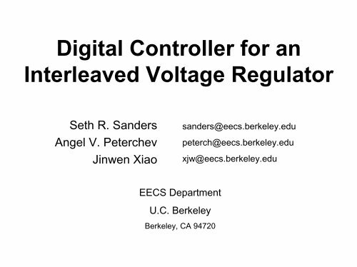
Digital Controller for an Interleaved Voltage Regulator - Inst.eecs ...
Digital Controller for an Interleaved Voltage Regulator - Inst.eecs ...
Digital Controller for an Interleaved Voltage Regulator - Inst.eecs ...

Create successful ePaper yourself
Turn your PDF publications into a flip-book with our unique Google optimized e-Paper software.
<strong>Digital</strong> <strong>Controller</strong> <strong>for</strong> <strong>an</strong><br />
<strong>Interleaved</strong> <strong>Voltage</strong> <strong>Regulator</strong><br />
Seth R. S<strong>an</strong>ders<br />
Angel V. Peterchev<br />
Jinwen Xiao<br />
s<strong>an</strong>ders@<strong>eecs</strong>.berkeley.edu<br />
peterch@<strong>eecs</strong>.berkeley.edu<br />
xjw@<strong>eecs</strong>.berkeley.edu<br />
EECS Department<br />
U.C. Berkeley<br />
Berkeley, CA 94720
DIGITAL PWM CONTROL<br />
— Motivation<br />
• Develop Low-Cost High-Flexibility <strong>Digital</strong><br />
<strong>Controller</strong>s <strong>for</strong> broad r<strong>an</strong>ge of PWM Control<br />
Applications (e.g. high quality power supply<br />
<strong>for</strong> next generation of Pentium CPU’s <strong>for</strong><br />
desktop <strong>an</strong>d portable computing)<br />
• Capture high frequency applications (>500<br />
KHz) not usually addressed with existing<br />
digital controllers
Why <strong>Digital</strong><br />
• Matching duty cycles among all phases in<br />
multi-phase converter, thus eliminating the<br />
need of current sensing at each phase<br />
• Immune to <strong>an</strong>alog component variations on<br />
chip<br />
• Implement sophisticated control schemes <strong>for</strong><br />
better per<strong>for</strong>m<strong>an</strong>ce<br />
• Programmable by a digital system like the<br />
CPU<br />
• Technology Scaling, shorter design period
Issues<br />
• <strong>Controller</strong> Architecture<br />
• Resolution—A/D, D/A<br />
• Development of control schemes that account<br />
<strong>for</strong> the non-linearity inherent in a qu<strong>an</strong>tized<br />
system<br />
• IC implementation of cost- <strong>an</strong>d powerefficient<br />
modules such as PWM generation<br />
<strong>an</strong>d A/D, D/A conversion functions
Application: 4-Phase Buck<br />
VRM
System Issues:<br />
Steady state limit cycling of V out resulting from qu<strong>an</strong>tization<br />
Vout<br />
1 bit error bin<br />
0 bit error bin<br />
tr<strong>an</strong>sient<br />
steady state<br />
DAC levels<br />
ADC levels<br />
-1 bit error bin
ADC <strong>an</strong>d DAC Resolution Requirements<br />
♦ Problem:<br />
Limit Cycling—Steady-state oscillations of Vout due to the<br />
qu<strong>an</strong>tization in the feedback loop.<br />
♦ Solution:<br />
— To ensure that there is a steady-state DAC (DPWM) level in<br />
the zero-error bin,<br />
resolution (DAC) > resolution (ADC)<br />
(a factor of 2 seems sufficient)<br />
—Slow Integrator to settle Vout to the zero-error bin of the ADC
Tr<strong>an</strong>sient response with res(DAC) = 2 • res(ADC) , <strong>an</strong>d<br />
<strong>an</strong> integrator<br />
Vout<br />
1 bit error bin<br />
tr<strong>an</strong>sient<br />
steady state<br />
0 bit error bin<br />
-1 bit error bin<br />
DAC levels<br />
ADC levels
Tr<strong>an</strong>sient Response without Integrator (simulation)<br />
Vin = 5 V , Vref = 2 V, res (ADC) = 8 bit , res (DAC) = 9 bit<br />
2.01<br />
2<br />
1.99<br />
1.98<br />
light load ← → heavy load<br />
↑<br />
reference voltage bin<br />
↓<br />
Limit cycling ↑<br />
in steady state<br />
V out<br />
1.97<br />
1.96<br />
1.95<br />
1.94<br />
ADC levels<br />
↓<br />
1.93<br />
1.92<br />
1.91<br />
1.5 2 2.5 3 3.5 4 4.5 5 5.5 6 6.5<br />
time (msec)
Tr<strong>an</strong>sient Response with Integrator (simulation)<br />
Vin = 5 V , Vref = 2 V, res (ADC) = 8 bit , res (DAC) = 9 bit<br />
2.01<br />
2<br />
1.99<br />
1.98<br />
↑<br />
reference voltage bin<br />
↓<br />
↑<br />
No limit cycling<br />
light load ← → heavy load<br />
in steady state<br />
V out<br />
1.97<br />
1.96<br />
1.95<br />
1.94<br />
ADC levels<br />
↓<br />
1.93<br />
1.92<br />
1.91<br />
1.5 2 2.5 3 3.5 4 4.5 5 5.5 6 6.5<br />
time (msec)
Introducing Sub-Bit Positioning<br />
♦ Problem:<br />
To provide accurate positioning of the output voltage at the<br />
order of 5 mV, the resolution of the DAC (DPWM) has to be 10<br />
bit with 5 V input. This resolution requires a DPWM module with<br />
a large number of stages running at a high frequency → high<br />
power dissipation.<br />
♦ Solution:<br />
Sub-Bit Positioning—use a DPWM module with lower<br />
hardware resolution (e.g. 7 or 8 bits) <strong>an</strong>d add digital dither to the<br />
duty cycle to produce finer (sub-bit) levels of Vout.
Structure <strong>for</strong> Adding Arbitrary Dither<br />
Patterns to the Duty Cycle<br />
f sw<br />
switching<br />
frequency<br />
D c<br />
duty cycle<br />
n + m<br />
m-bit<br />
counter<br />
m<br />
m (LSB’s)<br />
m x m<br />
look-up<br />
table<br />
1 (LSB)<br />
saturated<br />
n-bit<br />
adder<br />
n<br />
D c<br />
’<br />
dithered<br />
duty cycle<br />
n (MSB’s)
Dither Patterns Added To The Duty Cycle<br />
vs. Counter (Example For m = 2 Bits)<br />
counter<br />
Dc<br />
LSB’s<br />
00<br />
Sawtooth dither<br />
pattern<br />
00 01 10 11<br />
Modified dither<br />
pattern<br />
00 01 10 11<br />
Averaged<br />
sub-bit<br />
levels<br />
0<br />
01<br />
¼<br />
10<br />
½<br />
11<br />
¾<br />
T sw * 4<br />
T sw * 4<br />
♦ Modified dither patterns have higher frequency <strong>for</strong> some<br />
sub-bit levels, <strong>an</strong>d hence produce smaller ripple on Vout
Tr<strong>an</strong>sient Response with Sub-Bit Positioning<br />
Tr<strong>an</strong>sient Response with Sub-Bit Positioning<br />
11-bit ADC , 9-bit DAC + 3-bit SBP = effective effectve 12-bit DAC<br />
2.01<br />
2<br />
1.99<br />
↓<br />
↑<br />
reference voltage bin<br />
1.98<br />
V out<br />
1.97<br />
1.96<br />
1.95<br />
→ heavy load<br />
Vout finds a steady state<br />
within the reference bin due<br />
to the effective increase in<br />
DAC resolution<br />
1.94<br />
1.93<br />
1.92<br />
1.5 2 2.5 3 3.5 4 4.5 5 5.5 6<br />
time (msec)
Optimal <strong>Voltage</strong> Positioning<br />
What is it?<br />
Io max<br />
Load Step<br />
Iout<br />
∆I o<br />
Io min<br />
Usual converter<br />
response<br />
Vout<br />
2 * ∆I o *R esr<br />
Response with<br />
optimal voltage<br />
positioning<br />
Vout<br />
∆I o *R esr
Implementation of Optimal <strong>Voltage</strong> Positioning<br />
with I L<br />
<strong>an</strong>d I C<br />
sensing<br />
Vin<br />
Vref<br />
+<br />
_<br />
Ke<br />
error<br />
amplifier<br />
digital<br />
controller<br />
-<br />
L1<br />
I L<br />
Re<br />
Re*m<br />
Vc<br />
Co/m<br />
Re<br />
Co<br />
Iout<br />
Ic<br />
Vout<br />
-<br />
-<br />
Ic estimator<br />
Vo’ = Vout + Re * Iout<br />
Re * Iout = Re * (I L<br />
+ Ic) = Re * I L<br />
+ (Vc – Vout)<br />
Vo’ = Vc + Re * I L<br />
Adv<strong>an</strong>tage: Doesn’t add a resistive current sensor <strong>for</strong> Iout after Co (the voltage drop<br />
across such sensor would add to the ESR drop during tr<strong>an</strong>sients).
Tr<strong>an</strong>sient Response with <strong>Voltage</strong> Positioning (simulation)<br />
Vin = 5 V , Vref = 2 V, res (ADC) = 8 bit , res (DAC) = 9 bit<br />
2.02<br />
2<br />
1.98<br />
↑<br />
V out<br />
+ I out<br />
• R esr<br />
↑<br />
reference bin<br />
↓<br />
volts<br />
1.96<br />
1.94<br />
→ max load<br />
1.92<br />
V out<br />
↓<br />
1.9<br />
1 2 3 4 5 6<br />
time (msec)
Pro’s <strong>an</strong>d Con’s of <strong>Voltage</strong> Positioning<br />
Pro’s:<br />
♦ Resr c<strong>an</strong> be increased by a factor of 2<br />
Output capacitor size c<strong>an</strong> be reduced by a factor of 2.<br />
♦ Simple 3-level ADC (e.g. two comparators) c<strong>an</strong> be used, since<br />
the controlled qu<strong>an</strong>tity V o ’ has small excursions from the reference<br />
bin.<br />
Con’s:<br />
♦ Output current sensing required.<br />
♦ Value of Resr should be known.
Block Diagram of Proposed <strong>Controller</strong> Architecture<br />
with I L sensing <strong>an</strong>d I C estimation<br />
5 bit VID from<br />
microprocessor<br />
Vin<br />
Vref<br />
5,6bit<br />
slow<br />
DAC<br />
digital module<br />
feed<strong>for</strong>ward<br />
L1<br />
I L<br />
= Σ I Li<br />
all phases<br />
Vout<br />
+<br />
_<br />
Ke<br />
Ve<br />
error<br />
amplifier<br />
simple<br />
3,5-level<br />
ADC<br />
PID<br />
SBP<br />
DPWM<br />
-<br />
to other<br />
phases<br />
Re<br />
-<br />
Re*m<br />
Vc<br />
Co/m<br />
-<br />
Re<br />
Co<br />
Vo’ = Vout + Re * Iout<br />
♦ This architecture avoids individual sensing of the different phase currents
Step Response with <strong>Voltage</strong> Positioning <strong>an</strong>d Sub-Bit Positioning<br />
(simulation)<br />
V in<br />
= 5V, V ref<br />
= 2V, R esr<br />
= 3.5mΩ, ∆I = 10A,<br />
res(9-Bit ADC) = 10mV, res(DAC) = 5mV (7 bit + 3 bit dither = 10 bit)<br />
2.04<br />
2.02<br />
2<br />
steady-state<br />
(no limit cycling)<br />
ESR drop<br />
Tr<strong>an</strong>sient be<strong>for</strong>e the<br />
integrator has adjusted<br />
V out<br />
(V)<br />
1.98<br />
1.96<br />
1.94<br />
1.92<br />
1.9<br />
Load step<br />
∆I = 10A<br />
550 600 650 700 750 800 850 900 950 1000<br />
time (usec)
Step Response with <strong>Voltage</strong> Positioning <strong>an</strong>d Sub-Bit Positioning<br />
(test wave<strong>for</strong>m)<br />
V in<br />
= 5V, V ref<br />
= 2V, R esr<br />
= 3.5mΩ, ∆I = 10A,<br />
res(9-Bit ADC) = 10mV, res(DAC) = 5mV (7 bit + 3 bit dither = 10 bit)<br />
steady-state<br />
(no limit cycling)<br />
ESR drop<br />
tr<strong>an</strong>sient be<strong>for</strong>e the<br />
integrator has adjusted<br />
Load step<br />
∆I = 10A
PWM Generation Scheme<br />
— A Ring-Mux Structure
Ring Oscillator <strong>an</strong>d Multiplexer<br />
Detail
Test Wave<strong>for</strong>m (1)<br />
Differential outputs in one of 128 stages(1MHz)
Test Wave<strong>for</strong>m (2)<br />
Outputs of 2 adjacent stages, showing 1 LSB phase shift<br />
Oscillation Freq. = 1MHz, 1LSB = 1µs • 1/2 8 = 4ns<br />
4ns
PWM Generation Scheme 2<br />
— Counter-Comparator Structure <strong>for</strong> Phase 1
D-PWM generation Scheme<br />
Comparison<br />
Scheme Technology Clock<br />
(MHz)<br />
Counter- .5µm 5V 200MHz<br />
Comparator 1 (4x)<br />
Ring-Mux 2 .25µm 2.5V 100K-<br />
1MHz<br />
Area<br />
(µm×µm)<br />
1200×700<br />
(normalized to<br />
600×350)<br />
Power<br />
(µW)<br />
Hardware<br />
Sharing <strong>for</strong><br />
4 Phases<br />
50,000 LOW<br />
350×240 7.5 – 87.5 HIGH<br />
1. D-PWM has 10 bit resolution.<br />
2. D-PWM has effective 11 bit resolution, 8 MSB from the Ring-Mux<br />
structure <strong>an</strong>d its accessory circuit , 3 LSB from Sub-Bit Positioning.