Fast extraction of defect size distribution using a single ... - IEEE Xplore
Fast extraction of defect size distribution using a single ... - IEEE Xplore
Fast extraction of defect size distribution using a single ... - IEEE Xplore

Create successful ePaper yourself
Turn your PDF publications into a flip-book with our unique Google optimized e-Paper software.
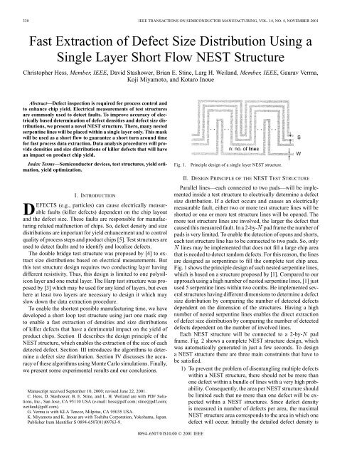
330 <strong>IEEE</strong> TRANSACTIONS ON SEMICONDUCTOR MANUFACTURING, VOL. 14, NO. 4, NOVEMBER 2001<strong>Fast</strong> Extraction <strong>of</strong> Defect Size Distribution Using aSingle Layer Short Flow NEST StructureChristopher Hess, Member, <strong>IEEE</strong>, David Stashower, Brian E. Stine, Larg H. Weiland, Member, <strong>IEEE</strong>, Gaurav Verma,Koji Miyamoto, and Kotaro InoueAbstract—Defect inspection is required for process control andto enhance chip yield. Electrical measurements <strong>of</strong> test structuresare commonly used to detect faults. To improve accuracy <strong>of</strong> electricallybased determination <strong>of</strong> <strong>defect</strong> densities and <strong>defect</strong> <strong>size</strong> <strong>distribution</strong>s,we present a novel NEST structure. There, many nestedserpentine lines will be placed within a <strong>single</strong> layer only. This maskwill be used as a short flow to guarantee a short turn around timefor fast process data <strong>extraction</strong>. Data analysis procedures will providedensities and <strong>size</strong> <strong>distribution</strong>s <strong>of</strong> killer <strong>defect</strong>s that will havean impact on product chip yield.Index Terms—Semiconductor devices, test structures, yield estimation,yield optimization.I. INTRODUCTIONDEFECTS (e.g., particles) can cause electrically measurablefaults (killer <strong>defect</strong>s) dependent on the chip layoutand the <strong>defect</strong> <strong>size</strong>. These faults are responsible for manufacturingrelated malfunction <strong>of</strong> chips. So, <strong>defect</strong> density and <strong>size</strong><strong>distribution</strong>s are important for yield enhancement and to controlquality <strong>of</strong> process steps and product chips [5]. Test structures areused to detect faults and to identify and localize <strong>defect</strong>s.The double bridge test structure was proposed by [4] to extract<strong>size</strong> <strong>distribution</strong>s based on electrical measurements. Butthis test structure design requires two conducting layer havingdifferent resistivity. Thus, this design is limited to one polysiliconlayer and one metal layer. The Harp test structure was proposedby [3] which may be used for any kind <strong>of</strong> layers, but evenhere at least two layers are necessary to design it which mayslow down the data <strong>extraction</strong> procedure.To enable the shortest possible manufacturing time, we havedeveloped a short loop test structure <strong>using</strong> just one mask stepto enable a fast <strong>extraction</strong> <strong>of</strong> densities and <strong>size</strong> <strong>distribution</strong>s<strong>of</strong> killer <strong>defect</strong>s that have a detrimental impact on the yield <strong>of</strong>product chips. Section II describes the design principle <strong>of</strong> theNEST structure, which enables the <strong>extraction</strong> <strong>of</strong> the <strong>size</strong> <strong>of</strong> eachdetected <strong>defect</strong>. Section III introduces the algorithms to determinea <strong>defect</strong> <strong>size</strong> <strong>distribution</strong>. Section IV discusses the accuracy<strong>of</strong> these algorithms <strong>using</strong> Monte Carlo simulations. Finally,we present some experimental results and our conclusions.Manuscript received September 10, 2000; revised June 22, 2001.C. Hess, D. Stashower, B. E. Stine, and L. H. Weiland are with PDF Solutions,Inc., San Jose, CA 95110 USA (e-mail: hess@pdf.com; stine@pdf.com;weiland@pdf.com).G. Verma is with KLA Tencor, Milpitas, CA 95035 USA.K. Miyamoto and K. Inoue are with Toshiba Corporation, Yokohama, Japan.Publisher Item Identifier S 0894-6507(01)09763-9.Fig. 1.Principle design <strong>of</strong> a <strong>single</strong> layer NEST structure.II. DESIGN PRINCIPLE OF THE NEST TEST STRUCTUREParallel lines—each connected to two pads—will be implementedinside a test structure to electrically determine a <strong>defect</strong><strong>size</strong> <strong>distribution</strong>. If a <strong>defect</strong> occurs and causes an electricallymeasurable fault, either two or more test structure lines will beshorted or one or more test structure lines will be opened. Themore test structure lines are involved, the larger the <strong>defect</strong> thatcaused this measured fault. In a 2-by- pad frame the number <strong>of</strong>pads is very limited. To enable the detection <strong>of</strong> opens and shorts,each test structure line has to be connected to two pads. So, onlylines may be implemented that does not fill a large chip areathat is needed to detect random <strong>defect</strong>s. For this reason, the linesare designed as serpentines to fill the complete test chip area.Fig. 1 shows the principle design <strong>of</strong> such nested serpentine lines,which is based on a structure proposed by [1]. Compared to ourapproach <strong>using</strong> a high number <strong>of</strong> nested serpentine lines, [1] justused 5 serpentine lines within two combs. He implemented severalstructures having different dimensions to determine a <strong>defect</strong><strong>size</strong> <strong>distribution</strong> by comparing the number <strong>of</strong> detected <strong>defect</strong>sdependent on the dimension <strong>of</strong> the structures. Having a highnumber <strong>of</strong> nested serpentine lines enables the direct <strong>extraction</strong><strong>of</strong> <strong>defect</strong> <strong>size</strong> <strong>distribution</strong> by comparing the number <strong>of</strong> detected<strong>defect</strong>s dependent on the number <strong>of</strong> involved lines.Each NEST structure will be connected to a 2-by- padframe. Fig. 2 shows a complete NEST structure design, whichwas automatically generated in just a few seconds. To designa NEST structure there are three main constraints that have tobe satisfied.1) To prevent the problem <strong>of</strong> disentangling multiple <strong>defect</strong>swithin a NEST structure, there should not be more thanone <strong>defect</strong> within a bundle <strong>of</strong> lines with a very high probability.Consequently, the area per NEST structure shouldbe limited such that no more than one <strong>defect</strong> will be expectedwithin a NEST structures. Since <strong>defect</strong> densityis measured in number <strong>of</strong> <strong>defect</strong>s per area, the maximalNEST structure area corresponds to the area in which one<strong>defect</strong> will occur. Initially the detailed <strong>defect</strong> density is0894–6507/01$10.00 © 2001 <strong>IEEE</strong>
HESS et al.: FAST EXTRACTION OF DEFECT SIZE DISTRIBUTION 331(a)Fig. 2. Design <strong>of</strong> a NEST structure containing 3104 parallel lines in a <strong>single</strong>metal layer.unknown, but usually an expected value can be obtainedfrom previous technologies. To be on the safe side, it isrecommended to use just half the maximal NEST structurearea, if it is based on an estimated <strong>defect</strong> density andnot on a measured <strong>defect</strong> density value.2) To keep the NEST structure measurable, the resistancevalue per line should be within the limits given by thetesting equipment.3) Testing time should be within a given limit per wafer,which will give the maximum number <strong>of</strong> pad frames andNEST structures that may be implemented within a die.Given today’s low expected <strong>defect</strong> densities, testing time usuallyis the main limitation for analog DC measurements <strong>using</strong> aparametric tester. For digital testing as described at [2] the lineresistance usually is the main limitation for the NEST structuredesign. To get reliable data for yield prediction for deep submicrometerprocesses where the average <strong>defect</strong> density is below0.5 <strong>defect</strong>s per cm , a large portion <strong>of</strong> the total area <strong>of</strong> a testchip has to be covered with NEST structures. Simulations withdifferent <strong>defect</strong> <strong>size</strong> <strong>distribution</strong>s as well as analyzing data fromseveral fabs lead to the following: For a complete lot <strong>of</strong> at least20 wafers no less than 30% <strong>of</strong> the test chip area should be filledwith NEST structures. If smaller lots with only 10–12 wafersare used, up to 50% <strong>of</strong> the test chip area is required for NESTstructures.III. DATA ANALYSIS PROCEDURESAfter briefly discussing the testing procedure <strong>of</strong> the NESTstructure, we will describe the algorithms to extract the <strong>size</strong> dis-(b)Fig. 3. (a) Number <strong>of</strong> <strong>defect</strong>s that have caused short circuits and (b) number <strong>of</strong><strong>defect</strong>s that have caused open circuits, both dependent on the number <strong>of</strong> lines.tribution <strong>of</strong> such <strong>defect</strong>s that have caused electrically measurablefaults within NEST structures.A. Testing <strong>of</strong> Opens and ShortsOpen circuits will be tested by measuring the resistancebetween the two pads connected to a <strong>single</strong> line <strong>of</strong> a NESTstructure. A given NEST structure <strong>of</strong> m lines will result in avector with m values each standing for a detected open line.The order <strong>of</strong> the values in the vector corresponds to the order<strong>of</strong> the lines within the NEST structure. For instance, the vector{0,0,1,1,0,0,0,0,0,1,1,1,0,0,0,0} <strong>of</strong> a NEST structure containinglines indicates that there are two open circuits. Oneopen circuit is caused by a <strong>defect</strong> interrupting the lines 3 and 4.The second open circuit is caused by a <strong>defect</strong> interrupting thelines 10, 11, and 12.Short circuits will be tested by measuring the resistancebetween two pads connected to adjacent lines. A given NESTstructure <strong>of</strong> lines will result in a vector with valueseach standing for a line being involved in a short circuit. Theorder <strong>of</strong> the values in the vector corresponds to the order <strong>of</strong>the lines within the NEST structure. For instance, the vector{0,0,0,0,0,1,1,1,0,0,0,0,0,1,1,0} <strong>of</strong> a NEST structure containinglines indicates that there are two short circuits. Oneshort circuit is caused by a <strong>defect</strong> connecting the lines 6, 7, and8. The second short circuit is caused by a <strong>defect</strong> connectingthe lines 14 and 15. Based on this we can generate a histogramfor open circuits as well as for short circuits as can be seen inFig. 3.
332 <strong>IEEE</strong> TRANSACTIONS ON SEMICONDUCTOR MANUFACTURING, VOL. 14, NO. 4, NOVEMBER 2001<strong>of</strong> a <strong>defect</strong> within the lines the <strong>defect</strong> can belong to one <strong>of</strong> thetwo possible adjacent intervals. So, for instance in Fig. 5 the <strong>defect</strong>s“ ” and “ ” can short either 3 or 4 lines although theyhave the same <strong>size</strong>. We have to summarize these overlappingintervals to get a <strong>size</strong> <strong>distribution</strong>. For that, it is useful to definethe following <strong>size</strong>-intervals where and :Fig. 4.Defects shorting internal and external lines <strong>of</strong> a NEST structure.(2)B. Defect Size Extraction <strong>of</strong> ShortsIn this section, we will describe in detail the procedure toextract a <strong>size</strong> <strong>distribution</strong> <strong>of</strong> such <strong>defect</strong>s that have caused shortcircuits.1) Internal and External Lines: At [3] an algorithm was presentedto extract a <strong>size</strong> <strong>distribution</strong> <strong>of</strong> <strong>defect</strong>s ca<strong>using</strong> short circuitswithin many electrically distinguishable parallel lines. AHarp test structure was used to provide such an environment.Within the NEST structure the electrically distinguishable linesare implemented as serpentines which will not always provideelectrically distinguishable neighbored lines. In Fig. 4 these socalled external lines are drawn as black lines. It can be seen thatthese lines only have an electrically “different” neighbor on oneside while they are neighbored to themselves at the other side.Only the so called internal lines (gray lines in Fig. 4) have electricallydistinguishable neighbored lines at all times.The possible <strong>size</strong> <strong>of</strong> a <strong>defect</strong> will be different if external linesare involved or not. For instance a <strong>defect</strong> <strong>of</strong> a given <strong>size</strong> as can beseen on the left side <strong>of</strong> Fig. 4 may short three internal lines. If thesame <strong>defect</strong> will hit an external line as can be seen on the rightside <strong>of</strong> this Fig. 4, only two lines are shorted. So, only for thosefaults exclusively connecting internal lines we can use an algorithmbased on [3], which will described in Section III-B2. Todetermine the <strong>defect</strong> <strong>size</strong> <strong>of</strong> those faults also including externallines, we will present a second algorithm in Section III-B3. Finally,both <strong>size</strong> <strong>distribution</strong>s will be summarized in a total <strong>defect</strong><strong>size</strong> <strong>distribution</strong>. To do so, we actually have to generate two histogramsas shown in Fig. 3, one just containing the shorts <strong>of</strong>internal lines and a second one containing the shorts that alsoinclude external lines.The external lines that are placed at the outer border <strong>of</strong> the entireNEST structure would theoretically require a third analysismethod since they are only neighbored to one line. However,due to the <strong>size</strong> <strong>of</strong> the NEST structure the fraction <strong>of</strong> these linesversus all other lines is so small that this effect can be neglected.2) Algorithm for Internal Lines: The number <strong>of</strong> connectedadjacent lines has to be transferred to a <strong>size</strong> <strong>distribution</strong> dependenton the design rules <strong>of</strong> the lines. For a given line widthand space , a <strong>defect</strong> that connects e.g., 2 lines may have a <strong>size</strong>in-between and . In general, a <strong>defect</strong> connectinglines may have a <strong>size</strong> in-betweenwhere is defined as the line pitch.Fig. 5 gives the range <strong>of</strong> possible <strong>defect</strong> <strong>size</strong>s for each number<strong>of</strong> connected lines. It can be seen, that there is an overlap betweenthe different intervals, because dependent on the position(1)The frequency <strong>of</strong> all detected <strong>defect</strong>s that connectexactly lines (ref. left side <strong>of</strong> Fig. 6) has to be distributedamong two <strong>size</strong> intervals. For that, <strong>defect</strong>s have to betransferred to the <strong>size</strong> interval representing the smallerfeature <strong>size</strong>s and <strong>defect</strong>s have to be transferred to the <strong>size</strong>interval representing the larger feature <strong>size</strong>s, where:So, for the number <strong>of</strong> <strong>defect</strong>s inside each<strong>size</strong>-interval will be:ifif .All these <strong>defect</strong> frequencies result in a <strong>size</strong> <strong>distribution</strong>illustrated on the right side <strong>of</strong> Fig. 6, where the fraction <strong>of</strong> andcan be seen again.Within the test chips, differently <strong>size</strong>d <strong>defect</strong>s result in differentnumbers <strong>of</strong> connected lines. So, the occurrence <strong>of</strong> <strong>defect</strong>sdependent on the number <strong>of</strong> connected lines always implicitlycontains the <strong>defect</strong> <strong>size</strong> <strong>distribution</strong> which occurs within themeasured test chips. So, we will use the ratio <strong>of</strong> adjacent <strong>defect</strong>occurrence value—as shown in charts like Fig. 3—to individuallycalculate the ratio <strong>of</strong>per <strong>size</strong> interval. Usinga design dependent weight factor , which will be described indetail in Section IV, will be calculated asandwill be calculated as3) Algorithm for External Lines: If external lines are involved,the possible range <strong>of</strong> <strong>defect</strong> <strong>size</strong>s is much larger thanfor the internal lines. So, for instance in Fig. 7 the <strong>defect</strong>s “ ”and “ ” can just short either 2 or 3 lines although they have thesame <strong>size</strong> than the <strong>defect</strong>s “ ” and “ ” <strong>of</strong> Fig. 5 that have connected3 or 4 lines. In other words, a two line short circuit canbe caused by a <strong>defect</strong> which <strong>size</strong> is in-between and .In general, a <strong>defect</strong> connecting lines may have a<strong>size</strong> in-between. This intervalis getting larger the more lines are involved compared tothe constant internal range for the internal line algorithm.For that, all <strong>defect</strong>s connecting n lines have to be distributednot just between two <strong>defect</strong> <strong>size</strong> intervals but between anifif(3)(4)(5)(6)
HESS et al.: FAST EXTRACTION OF DEFECT SIZE DISTRIBUTION 333Fig. 5.Link between the <strong>size</strong> intervals SI(X) and the possible <strong>size</strong> <strong>of</strong> a <strong>defect</strong> ca<strong>using</strong> a short circuit over n lines.Fig. 6.Transition from the number <strong>of</strong> <strong>defect</strong>s dependent on the number <strong>of</strong> involved lines to the <strong>defect</strong> <strong>size</strong> <strong>distribution</strong>.Fig. 7.Link between the <strong>size</strong> intervals SI(X) and the possible <strong>size</strong> <strong>of</strong> a <strong>defect</strong> ca<strong>using</strong> a short circuit over n internal and external lines.increasing number <strong>of</strong> <strong>defect</strong> <strong>size</strong> intervals. Furthermore, weusually observe much more faults just connecting internallines because there are much more internal lines than externallines designed within a NEST structure. So, the sample <strong>size</strong><strong>of</strong> <strong>defect</strong>s involving external lines is too small to give areasonable <strong>defect</strong> <strong>size</strong> <strong>distribution</strong> on its own.Instead, we will use the <strong>size</strong> <strong>distribution</strong> already determinedfor such <strong>defect</strong>s just connecting internal lines to distribute the
334 <strong>IEEE</strong> TRANSACTIONS ON SEMICONDUCTOR MANUFACTURING, VOL. 14, NO. 4, NOVEMBER 2001<strong>defect</strong>s that connect also external lines among the different <strong>defect</strong><strong>size</strong> intervals. So, based on the number <strong>of</strong> faults thathave shorted n lines, the following equation will determine thenumber <strong>of</strong> <strong>defect</strong>s per <strong>size</strong> intervalifif(7)where is the number <strong>of</strong> <strong>defect</strong>s per <strong>size</strong> interval <strong>of</strong>the <strong>defect</strong> <strong>size</strong> <strong>distribution</strong> determined in Section III-B2 for the<strong>defect</strong>s involving internal lines only.4) Total Defect Size Distribution: Finally, per <strong>size</strong> intervalwe summarize the two <strong>defect</strong> count values <strong>of</strong> the internaland external <strong>defect</strong> <strong>size</strong> <strong>distribution</strong> charts. Theresulting histogram will give a <strong>size</strong> <strong>distribution</strong> <strong>of</strong> all <strong>defect</strong>s thathave caused electrically measurable faults within NEST structures.The ratio <strong>of</strong> faults including an external line versus faults justincluding internal lines should be about , where isthe number <strong>of</strong> electrically distinguishable lines within a NESTstructure. This may be used as a sanity check regarding possiblesystematic process problems.C. Defect Size Extraction for OpensThe same procedure described for short circuits can be usedto extract a <strong>size</strong> <strong>distribution</strong> <strong>of</strong> <strong>defect</strong>s that have caused electricallymeasurable open circuits. To do so, the following transformationshave to be applied to the algorithms described inSections III-B2 and III-B3:1) The smallest number <strong>of</strong> open lines start atcompared to in case <strong>of</strong> short circuits. So, due toequation (4) will change to:ifif .(8)2) The width and space <strong>of</strong> the lines within the NESTstructure have to be exchanged regarding the <strong>defect</strong> <strong>size</strong>intervals. So, a <strong>defect</strong> opening internal lines mayhave a <strong>size</strong> in-between .Consequently, the <strong>size</strong>-intervals will be defined as:3) Defects that open internal and external lines mayhave a <strong>size</strong> inbetween. Based on this, the following equation will replaceequation (7) to determine the number <strong>of</strong> <strong>defect</strong>s(9)Fig. 8. Comparison <strong>of</strong> the <strong>size</strong> <strong>distribution</strong> <strong>of</strong> 412 simulated <strong>defect</strong>s and the<strong>size</strong> <strong>distribution</strong> <strong>of</strong> those <strong>defect</strong>s that where detected as faults within a NESTstructure.per <strong>size</strong> intervalifif .IV. SIMULATION OF DEFECT SIZE DISTRIBUTIONS(10)To determine the factor we set up various Monte Carlo simulationsfor different sets <strong>of</strong> <strong>defect</strong>s. Per experiment we generated500 <strong>defect</strong>s on average and throw them on NEST structureshaving different dimensions. Based on the number <strong>of</strong> shortedlines we used the algorithms described in Section III to determinea <strong>defect</strong> <strong>size</strong> <strong>distribution</strong>. We then compared such aNEST based <strong>defect</strong> <strong>size</strong> <strong>distribution</strong> to the <strong>defect</strong> <strong>size</strong> <strong>distribution</strong>based on the actual <strong>defect</strong>s that were thrown on the NESTstructures. One example for a <strong>defect</strong> <strong>distribution</strong> proportionalto can be seen in the Fig. 8. Another example for a <strong>defect</strong><strong>distribution</strong> proportional to can be seen in Fig. 9.Except for the smallest <strong>size</strong> interval, we obtained the best fitsfor regardless <strong>of</strong> the <strong>defect</strong> <strong>size</strong> <strong>distribution</strong>s we chooseand the dimensions we choose for the NEST structures. For thesmallest <strong>size</strong> interval we always observe a much smaller number<strong>of</strong> <strong>defect</strong>s within the NEST structure than there is according tothe assumed <strong>defect</strong> <strong>size</strong> <strong>distribution</strong>, because not all <strong>defect</strong>s thatare smaller than the line width plus twice the line space <strong>of</strong> aNEST structure will actually result in electrically measurableshort circuits. To evaluate whether such an error has a significanteffect on yield prediction we studied the yield impact on productchips. For that, we determined the cumulative critical area forseveral typical product chips as one can be seen in Fig. 10. Thedifferent curves in this graph show the different cumulative criticalarea curves for 2 line shorts, 3-line shorts, 4-line shorts,
HESS et al.: FAST EXTRACTION OF DEFECT SIZE DISTRIBUTION 335Fig. 9. Comparison <strong>of</strong> the <strong>size</strong> <strong>distribution</strong> <strong>of</strong> 505 simulated <strong>defect</strong>s and the<strong>size</strong> <strong>distribution</strong> <strong>of</strong> those <strong>defect</strong>s that where detected as faults within a NESTstructure.Fig. 11. Yield impact <strong>of</strong> different simulated <strong>defect</strong> <strong>size</strong> <strong>distribution</strong>s on aproduct chip.TABLE IDIMENSIONS OF NEST STRUCTURES TO EVALUATE DEEP SUBMICROMETERINTERCONNECTION LAYERFig. 10. Cumulative critical area curves <strong>of</strong> a typical product chip for 2-lineshorts, 3-line shorts, 4-line shorts, 5-line shorts, and 6-line shorts.5-line shorts, and 6-line shorts. Only the 2-line shorts and the3-line shorts have some critical areas in the small <strong>size</strong> region weare interested in. The yield impact is proportional to the integral<strong>of</strong> the critical area multiplied by the <strong>defect</strong> <strong>size</strong> <strong>distribution</strong> ascan be seen in Fig. 11 for different <strong>defect</strong> <strong>size</strong> <strong>distribution</strong>s. Itcan be seen that the yield impact for the smallest <strong>defect</strong> <strong>size</strong> intervalis less than 5%. So, even a relatively large error in thisregion is acceptable if it comes to yield prediction.V. EXPERIMENTAL RESULTSAt Toshiba Corporation in Yokohama, Japan, several NESTstructures were manufactured to control <strong>defect</strong> appearance in adeep submicron backend environment. Table I summarizes thestructures used to extract <strong>defect</strong> <strong>size</strong> <strong>distribution</strong>s. Using differentlydimensioned NEST structures enables the separation <strong>of</strong>systematic and random <strong>defect</strong>s. So, for instance there will beno systematic yield issues only if the <strong>defect</strong> density values <strong>of</strong>differently dimensioned NEST structures follow a poisson <strong>distribution</strong>.If <strong>defect</strong>s occur and cause a fault, either test structureFig. 12. Size <strong>distribution</strong> <strong>of</strong> <strong>defect</strong>s detected within a 0.56-m line pitch(0.28-m line width) NEST structure.lines are connected to each other or test structure lines are interrupted.Since we know which test structure lines are implementedas neighbors, we can conclude to the number and <strong>size</strong> <strong>of</strong>the <strong>defect</strong>s. Based on the number <strong>of</strong> shorted lines we apply thealgorithms introduced in Section III to determine a <strong>defect</strong> <strong>size</strong><strong>distribution</strong> as can be seen in Figs. 12 and 13. If for yield predictionpurposes these measured <strong>defect</strong> <strong>size</strong> <strong>distribution</strong>s should bemodeled by an analytical function or calibrated to an analytical
336 <strong>IEEE</strong> TRANSACTIONS ON SEMICONDUCTOR MANUFACTURING, VOL. 14, NO. 4, NOVEMBER 2001analysis requirements discussed in that paper. SEM pictures <strong>of</strong>two detected <strong>defect</strong>s can be seen in Figs. 14 and 15. The sameprinciple could be applied for opens, but the observed <strong>defect</strong>density was too small to actually generate a significant <strong>defect</strong><strong>size</strong> histogram.Fig. 13. Size <strong>distribution</strong> <strong>of</strong> <strong>defect</strong>s detected within a 0.44-m line pitch(0.22 -m line width) NEST structure.VI. CONCLUSIONThe described method to place test structure lines enables afast and efficient inspection <strong>of</strong> <strong>defect</strong>s that occur in a <strong>single</strong>layer. Just <strong>using</strong> a <strong>single</strong> short loop mask guarantees a shortturn around time for fast process controlling. There is no limitationregarding layer specific properties such as sheet resistanceand no requirement <strong>of</strong> any semiconductor devices to separatetest structure lines or disentangle multiple faults, respectively.The NEST structure detects systematic problems as wellas random <strong>defect</strong>s to determine accurate <strong>defect</strong> densities and<strong>size</strong> <strong>distribution</strong>s.ACKNOWLEDGMENTThe authors would like to thank R. Burch, PDF Solutions Inc.,for the Monte Carlo simulations and many valuable analysisdiscussions.Fig. 14. Detected <strong>defect</strong> that has caused an electrically measurable shortcircuit between 2 lines.REFERENCES[1] R. Glang, “Defect <strong>size</strong> <strong>distribution</strong> in VLSI chips,” <strong>IEEE</strong> Trans. Semiconduct.Manufact., vol. 4, pp. 265–269, Nov. 1991.[2] C. Hess and L. H. Weiland, “A digital tester based measurementmethodology for process control in multilevel metallization systems,”in Proc. 1995 SPIE Microelectronic Manufacturing, vol. 2637, 1995,pp. 125–136.[3] , “Harp test structure to electrically determine <strong>size</strong> <strong>distribution</strong>s<strong>of</strong> killer <strong>defect</strong>s,” <strong>IEEE</strong> Trans. Semiconduct. Manufact., vol. 11, pp.194–203, May 1998.[4] J. B. Khare, W. Maly, and M. E. Thomas, “Extraction <strong>of</strong> <strong>defect</strong> <strong>size</strong><strong>distribution</strong>s in an IC layer <strong>using</strong> test structure data,” <strong>IEEE</strong> Trans. Semiconduct.Manufact., vol. 7, pp. 354–368, Aug. 1994.[5] C. H. Staper and R. J. Rosner, “Integrated circuit yield management andyield analysis: Development and implementation,” <strong>IEEE</strong> Trans. Semiconduct.Manufact., vol. 8, pp. 95–102, May 1995.Fig. 15. Detected <strong>defect</strong> that has caused an electrically measurable shortcircuit between 11 lines.function, it is possible to use the method describe at [4] since theNEST structure is fully compatible with the measurement andChristopher Hess (S’94–A’98–M’00) was born inWiesbaden, Germany. He received the Dipl. degreein electrical engineering from the University <strong>of</strong> Karlsruhe,Germany, in 1992, and the Dr.-Ing. (Ph.D.) degreein computer science from the University <strong>of</strong> Karlsruhe,Germany, in 1998.In 1992, he joined the Institute <strong>of</strong> Computer Designand Fault Tolerance at the University <strong>of</strong> Karlsruheas a founding member <strong>of</strong> the Defect DiagnosisGroup. In 1998, he moved to the U.S. and joined PDFSolutions, San Jose, CA, as a Senior Consulting Engineer.He currently holds a position as Manager, Yield Design Modeling. Since1992, he has been involved in the design <strong>of</strong> more than 50 test chips for the microelectronicsindustry in several areas which include copper metallization processing,yield and performance enhancement, as well as microelectronic teststructures for the <strong>extraction</strong> <strong>of</strong> <strong>defect</strong> <strong>size</strong> <strong>distribution</strong>s and the characterization<strong>of</strong> failure modes in integrated circuits. He has developed yield ramp test structuresthat allow fast and efficient testing, which is key to wafer-level and lot-leveldata acquisition and analysis that is required for statistical process control targetingyield and performance improvements. He has authored or coauthoredmore than 30 conference and journal papers. His research interests include <strong>defect</strong>detection and localization techniques as well as <strong>defect</strong> analysis in semiconductormanufacturing processes.Dr. Hess is a Member <strong>of</strong> the <strong>IEEE</strong> Electron Devices Society. He is a TechnicalCommittee Member <strong>of</strong> several semiconductor manufacturing related conferencesand has served as Technical Chairman <strong>of</strong> the 2000 International Conferenceon Microelectronic Test Structures held in Monterey, CA.
HESS et al.: FAST EXTRACTION OF DEFECT SIZE DISTRIBUTION 337David Stashower received the B.S. degree in engineeringphysics from the University <strong>of</strong> California,Berkeley.He is a Manager <strong>of</strong> Data Operations in PDF Solutions’Yield Analysis Group. He has also lead effortsin the design, implementation, and analysis <strong>of</strong> testvehicles; in support <strong>of</strong> PDF’s service engagements.Prior to joining PDF, he worked in device and yieldengineering and CIM organizations at Motorola andWestern Digital.Gaurav Verma received the B.A. degree in physics from Ohio Wesleyan University,Delaware, OH, in 1992, and is currently working toward the Ph.D. degreein materials science and engineering at Stanford University, Stanford, CA.His research in graduate school was primarily focused on integration issuesrelated to laser thermal processing (LTP) <strong>of</strong> semiconductors. He did work onfabrication and studied phase transformation characteristics <strong>of</strong> ultra-shallowsalicides fabricated <strong>using</strong> LTP. He also worked on fabrication <strong>of</strong> highly doped,abrupt, ultra-shallow junctions <strong>using</strong> LTP. Since 1999, he has been involved insemiconductor yield ramp and modeling issues with PDF Solutions and mostrecently with KLA Tencor.Brian E. Stine received the B.S. (summa cumlaude) and the M.S. degrees in electrical engineeringfrom the University <strong>of</strong> Pennsylvania, Philadelphia,and the Ph.D. degree in electrical engineering andcomputer science from the Massachusetts Institute<strong>of</strong> Technology, Cambridge.His dissertation dealt with assessing and modelingspatial variation in semiconductor processes and withestimating the their impact on circuit performanceand manufacturability. Most <strong>of</strong> this work focused onChemical Mechanical Polishing (CMP). He was anIntel Graduate Fellow in 1997. He is currently a Director in the client servicesorganization <strong>of</strong> PDF Solutions, Inc., San Jose, CA. His work mostly focuses onaccelerating yield ramps <strong>of</strong> system on chip products for 0.18 m, 0.13 m, andbelow technology nodes for key clients in the Japanese semiconductor market.Larg H. Weiland (S’94–M’98) was born in Konstanz,Germany. He received the Dipl. degree inphysics from the University <strong>of</strong> Karlsruhe, Germany,in 1992, and the Dr.-Ing. (Ph.D.) degree in computerscience from the University <strong>of</strong> Karlsruhe, Germany,in 1998.In 1993, he joined Institute <strong>of</strong> Computer Designand Fault Tolerance at the University <strong>of</strong> Karlsruhe.There, he was C<strong>of</strong>ounder <strong>of</strong> the Defect DiagnosisGroup. In 1998, he joined PDF Solutions Inc. inSan Jose, CA. Since 2000, he has managed theTest Structure Design Automation Group at PDF. In 1998, he joined theorganizing committee <strong>of</strong> the SPIE Microelectronic and MEMS Technologiesconference. He has chaired a number <strong>of</strong> test structure and manufacturing relatedconferences like ICMTS, ASMC and SPIE’s Microelectronic Manufacturing.He has authored or coauthored over 30 journal and conference papers. He isinvolved with the microelectronics industry in several areas, which includemetallization processing, test structure design automation, digital and opticalmeasurements on test chips and fast <strong>defect</strong> diagnosis from digital tester data.His research interests include physics <strong>of</strong> <strong>defect</strong> mechanisms in semiconductormanufacturing processes.Dr. Weiland is Member <strong>of</strong> the <strong>IEEE</strong> Electron Device Society.Koji Miyamoto received the B.E. and M.E. degreesin electrical engineering from Hosei University,Tokyo, Japan, in 1985 and 1987, respectively.He joined LSI division II, Toshiba Corporation,Kawasaki, Japan, in 1987. He has been engagedin the development <strong>of</strong> process, device, and yieldmanagement technology for advanced CMOS logicand embedded memories. He also has been engagedin the development <strong>of</strong> information technology forconcurrent engineering work.Dr. Miyamoto is a Member <strong>of</strong> <strong>IEEE</strong> Electron DeviceSociety.Kohtaro Inoue received the B.E. degree in physicsfrom Aoyama Gakuin University, Tokyo, Japan, in1989.He joined LSI division II, Toshiba Corporation,Kawasaki, Japan, in 1989. He had been engaged inthe development for process and device technology<strong>of</strong> BiCMOS logic from 1989 to 1994. He is currentlyworking on Yield Management for CMOS SystemLSI.