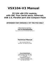
VDX104 Manual - Tri-M Systems Inc.
VDX104 Manual - Tri-M Systems Inc.
VDX104 Manual - Tri-M Systems Inc.

Create successful ePaper yourself
Turn your PDF publications into a flip-book with our unique Google optimized e-Paper software.
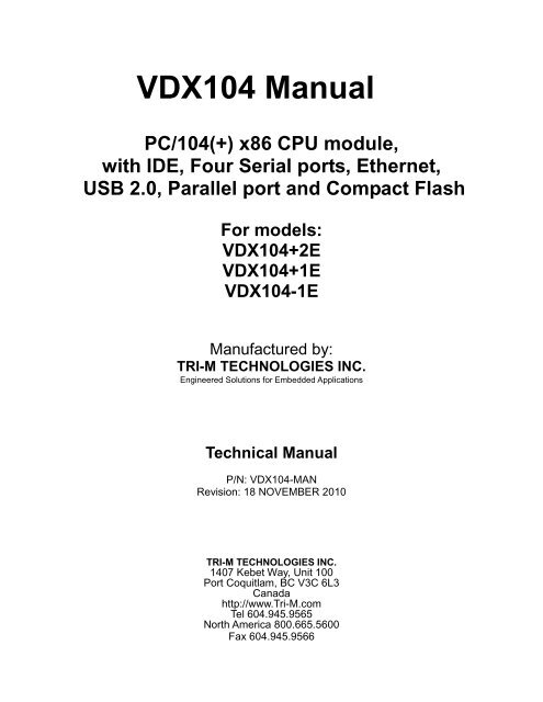
<strong>VDX104</strong> <strong>Manual</strong><br />
PC/104(+) x86 CPU module,<br />
with IDE, Four Serial ports, Ethernet,<br />
USB 2.0, Parallel port and Compact Flash<br />
For models:<br />
<strong>VDX104</strong>+2E<br />
<strong>VDX104</strong>+1E<br />
<strong>VDX104</strong>-1E<br />
Manufactured by:<br />
TRI-M TECHNOLOGIES INC.<br />
Engineered Solutions for Embedded Applications<br />
Technical <strong>Manual</strong><br />
P/N: <strong>VDX104</strong>-MAN<br />
Revision: 18 NOVEMBER 2010<br />
TRI-M TECHNOLOGIES INC.<br />
1407 Kebet Way, Unit 100<br />
Port Coquitlam, BC V3C 6L3<br />
Canada<br />
http://www.<strong>Tri</strong>-M.com<br />
Tel 604.945.9565<br />
North America 800.665.5600<br />
Fax 604.945.9566
PREFACE<br />
This manual is for integrators of applications of embedded systems. It contains information on hardware<br />
requirements and interconnection to other embedded electronics.<br />
DISCLAIMER<br />
<strong>Tri</strong>-M Technologies <strong>Inc</strong>. makes no representations or warranties with respect to the contents of this manual,<br />
and specifically disclaims any implied warranties of merchantability or fitness for any particular purpose. <strong>Tri</strong>-M<br />
Technologies <strong>Inc</strong>. shall under no circumstances be liable for incidental or consequential damages or related<br />
expenses resulting from the use of this product, even if it has been notified of the possibility of such damages.<br />
<strong>Tri</strong>-M Technologies <strong>Inc</strong>. reserves the right to revise this publication from time to time without obligation to notify<br />
any person of such revisions. If errors are found, please contact <strong>Tri</strong>-M Technologies <strong>Inc</strong>. at the address listed<br />
on the title page of this document.<br />
COPYRIGHT © 2008-05-30 TRI-M TECHNOLOGIES INC.<br />
No part of this document may be reproduced, transmitted, transcribed, stored in a retrieval system, or<br />
translated into any language or computer language, in any form or by any means, electronic, mechanical,<br />
magnetic, optical, chemical, manual, or otherwise, without the express written permission of <strong>Tri</strong>-M<br />
Technologies <strong>Inc</strong>..
18-Nov-2010<br />
<strong>VDX104</strong> <strong>Manual</strong><br />
CHAPTER 1: GENERAL DESCRIPTION ............................................................................................. 6<br />
1.1 SPECIFICATIONS/FEATURES .............................................................................................................................................................. 6<br />
1.1.1 Vortex86DX ............................................................................................................................................................................ 6<br />
1.1.2 Memory .................................................................................................................................................................................... 6<br />
1.1.3 RS232 Interface ....................................................................................................................................................................... 6<br />
1.1.4 Universal Serial Bus Interface ................................................................................................................................................ 6<br />
1.1.5 Ethernet Interface .................................................................................................................................................................... 6<br />
1.1.6 Parallel Interface .................................................................................................................................................................... 7<br />
1.1.7 Keyboard/Mouse Interface ...................................................................................................................................................... 7<br />
1.1.8 Enhanced IDE Interface .......................................................................................................................................................... 7<br />
1.1.9 On board backup battery ......................................................................................................................................................... 7<br />
1.1.10 Expansion BUS - PC/104+ signals ....................................................................................................................................... 7<br />
1.1.11 Flash Storage ......................................................................................................................................................................... 7<br />
1.1.12 Jumperless configuration ...................................................................................................................................................... 7<br />
1.1.13 Software Compatibility .......................................................................................................................................................... 7<br />
1.1.14 Mechanical/Environmental.................................................................................................................................................... 7<br />
CHAPTER 2: INSTALLATION ............................................................................................................. 8<br />
2.1 LOCATING THE TOP CONNECTORS ..................................................................................................................................................... 8<br />
2.2 LOCATING THE BOTTOM CONNECTORS ............................................................................................................................................. 9<br />
CHAPTER 3: JUMPERS .................................................................................................................... 10<br />
CHAPTER 4: CONNECTORS ............................................................................................................ 11<br />
4.1 COMPACT FLASH SOCKET (CN1) ................................................................................................................................................... 12<br />
4.2 IDE INTERFACE (CN2) ................................................................................................................................................................... 13<br />
4.3 SERIAL PORTS RS232 (CN8, CN9, CN10 AND CN11) .................................................................................................................... 14<br />
4.4 PARALLEL PORT (CN12)................................................................................................................................................................. 14<br />
4.5 UNIVERSAL SERIAL BUS (CN13) .................................................................................................................................................... 15<br />
4.6 MICROSD SOCKET (CN14) <strong>VDX104</strong>+2E ONLY ............................................................................................................................. 15<br />
4.7 USB DEVICE PORT (CN15) <strong>VDX104</strong>+2E ONLY ............................................................................................................................. 16<br />
4.8 REDUNDANCY PORT AND I2C (CN16) ............................................................................................................................................ 16<br />
4.9 PS/2-SPI PORT (CN17) .................................................................................................................................................................. 17<br />
4.10 JTAG PORT (CN18) ..................................................................................................................................................................... 18<br />
4.11 PC/104 BUS (CN19 AND CN21) .................................................................................................................................................. 19<br />
4.12 PC/104+ BUS (CN20) <strong>VDX104</strong>+1E & <strong>VDX104</strong>+2E ONLY ........................................................................................................ 21<br />
4.13 LAN INTERFACE 1 (CN22) ........................................................................................................................................................... 22<br />
4.14 LAN INTERFACE 2 (CN23) <strong>VDX104</strong>+2E ONLY ........................................................................................................................... 22<br />
4.15 INPUT POWER (CN24) .................................................................................................................................................................. 23<br />
4.16 GPIO 0 PORT (CN26) ................................................................................................................................................................... 24<br />
4.17 ON-BOARD USB 2.0 EXTENSION MODULE (CN32) ....................................................................................................................... 24<br />
CHAPTER 5: GENERAL PURPOSE INPUT/OUPUT ....................................................................... 25<br />
5.1 OVERVIEW ..................................................................................................................................................................................... 25<br />
5.2 GPIO PORT 0 ................................................................................................................................................................................. 25<br />
5.3 GPIO PORT 1 ................................................................................................................................................................................. 26<br />
5.4 GPIO PORT 2 ................................................................................................................................................................................. 27<br />
5.5 GPIO PORT 3 ................................................................................................................................................................................. 28<br />
5.6 GPIO PORT 4 ................................................................................................................................................................................. 29<br />
<strong>Tri</strong>-M Technologies <strong>Inc</strong>. Tel: 800.665.5600, 604.945.9565<br />
1407 Kebet Way, Unit 100 Fax: 604.945.9566<br />
Port Coquitlam, BC V3C 6L3 E-mail: info@tri-m.com<br />
Canada Web site: www.tri-m.com 3
18-Nov-2010<br />
<strong>VDX104</strong> <strong>Manual</strong><br />
CHAPTER 6: WATCHDOG TIMER ................................................................................................... 30<br />
6.1 OVERVIEW ..................................................................................................................................................................................... 30<br />
6.2 WDT0 REGISTERS ......................................................................................................................................................................... 30<br />
6.3 WDT1 REGISTERS ......................................................................................................................................................................... 32<br />
CHAPTER 7: CMOS RAM ................................................................................................................. 34<br />
7.1 OVERVIEW ..................................................................................................................................................................................... 34<br />
7.2 CMOS RAM MAPPING .................................................................................................................................................................. 34<br />
CHAPTER 8: REDUNDANCY ........................................................................................................... 35<br />
8.1 OVERVIEW ..................................................................................................................................................................................... 35<br />
8.2 BLOCK DIAGRAM ........................................................................................................................................................................... 35<br />
8.3 TRI-STATED DEVICES ..................................................................................................................................................................... 36<br />
8.4 SYSTEM INTERCOMMUNICATION ................................................................................................................................................... 36<br />
CHAPTER 9: ONBOARD SPI FLASH (<strong>VDX104</strong>+2E ONLY) ............................................................. 37<br />
9.1 OVERVIEW ..................................................................................................................................................................................... 37<br />
9.2 SPITOOL ........................................................................................................................................................................................ 37<br />
CHAPTER 10: ONBOARD LED'S ...................................................................................................... 38<br />
10.1 OVERVIEW ................................................................................................................................................................................... 38<br />
10.2 LED1 .......................................................................................................................................................................................... 38<br />
10.3 LED2 (<strong>VDX104</strong>+2E ONLY) ......................................................................................................................................................... 38<br />
10.4 LED3 .......................................................................................................................................................................................... 38<br />
10.5 LED4 (<strong>VDX104</strong>+2E ONLY) ......................................................................................................................................................... 38<br />
CHAPTER 11: CONSOLE REDIRECTION ........................................................................................ 39<br />
11.1OVERVIEW .................................................................................................................................................................................... 39<br />
11.2FORCE CONSOLE REDIRECTION ON ............................................................................................................................................. 39<br />
11.3DEFAULT SETTINGS ....................................................................................................................................................................... 39<br />
CHAPTER 12: BIOS ........................................................................................................................... 40<br />
12.1 MAIN MENU ................................................................................................................................................................................. 40<br />
12.2 ADVANCED SETTINGS ................................................................................................................................................................... 41<br />
12.3 CPU CONFIGURATION .................................................................................................................................................................. 42<br />
12.4 IDE CONTROLLER CONFIGURATION ............................................................................................................................................. 43<br />
12.5 IDE DEVICES CONFIGURATION .................................................................................................................................................... 44<br />
12.6 CONSOLE REDIRECTION CONFIGURATION .................................................................................................................................... 45<br />
12.7 USB CONTROLLER CONFIGURATION ............................................................................................................................................ 46<br />
12.8 USB STORAGE DEVICES CONFIGURATION ................................................................................................................................... 47<br />
12.9 PCI/PNP CONFIGURATION ........................................................................................................................................................... 48<br />
12.10 BOOT MENU ............................................................................................................................................................................... 50<br />
12.11 BOOT OPTIONS ........................................................................................................................................................................... 51<br />
12.12 BOOT PRIORITY OVERALL .......................................................................................................................................................... 52<br />
12.13 BOOT PRIORITY FOR HARD-DRIVE.............................................................................................................................................. 53<br />
12.14 BOOT PRIORITY FOR REMOVABLE DEVICE ................................................................................................................................. 54<br />
12.15 SECURITY CONFIGURATION ........................................................................................................................................................ 55<br />
12.16 CHIPSET SUB-MENU .................................................................................................................................................................... 56<br />
12.17 NORTHBRIDGE CONFIGURATION ................................................................................................................................................ 57<br />
12.18 SOUTHBRIDGE CONFIGURATION ................................................................................................................................................ 58<br />
12.19 ISA CLOCK SETTINGS ................................................................................................................................................................. 59<br />
<strong>Tri</strong>-M Technologies <strong>Inc</strong>. Tel: 800.665.5600, 604.945.9565<br />
1407 Kebet Way, Unit 100 Fax: 604.945.9566<br />
Port Coquitlam, BC V3C 6L3 E-mail: info@tri-m.com<br />
Canada Web site: www.tri-m.com 4
18-Nov-2010<br />
<strong>VDX104</strong> <strong>Manual</strong><br />
12.20 SERIAL/PARALLEL PORTS CONFIGURATION ................................................................................................................................ 60<br />
12.21 WATCHDOGS CONFIGURATION ................................................................................................................................................... 62<br />
12.22 MULTI-FUNCTION PORTS SUB-MENU .......................................................................................................................................... 63<br />
12.23 GPCS CONFIGURATION .............................................................................................................................................................. 72<br />
12.24 REDUNDANCY PORT CONFIGURATION ........................................................................................................................................ 73<br />
12.25 EXIT OPTIONS ............................................................................................................................................................................ 75<br />
CHAPTER 13: LITERATURE REFERENCES .................................................................................... 76<br />
13.1 ISA SYSTEM ARCHITECTURE ....................................................................................................................................................... 76<br />
13.2 AT BUS DESIGN ............................................................................................................................................................................ 76<br />
13.3 PERSONAL COMPUTER BUS STANDARD P996 ............................................................................................................................... 76<br />
13.4 PC INTERRUPTS ............................................................................................................................................................................ 76<br />
13.5 PC/104 CONSORTIUM ................................................................................................................................................................... 76<br />
<strong>Tri</strong>-M Technologies <strong>Inc</strong>. Tel: 800.665.5600, 604.945.9565<br />
1407 Kebet Way, Unit 100 Fax: 604.945.9566<br />
Port Coquitlam, BC V3C 6L3 E-mail: info@tri-m.com<br />
Canada Web site: www.tri-m.com 5
18-Nov-2010<br />
<strong>VDX104</strong> <strong>Manual</strong><br />
CHAPTER 1: GENERAL DESCRIPTION<br />
The <strong>VDX104</strong> is a PC104 or PC/104+ compliant system controller measuring just 3.55 inches by 3.775 inches.<br />
The <strong>VDX104</strong> offers the quickest route of integrating a full x86 AT-compatible computer into your embedded<br />
control application using the PC/104 or PC/104+ form factor. In addition, the built-in peripherals minimize the<br />
number of additional modules required. By combining the system hardware, I/O, software (integrated OS<br />
image) and solid-state mass storage, the <strong>VDX104</strong> lowers your exposure to possible development risks, costs<br />
and significantly reduces your time-to-market.<br />
The <strong>VDX104</strong>’s full compatibility with the popular PC/104 or PC/104+ embedded expansion bus allows you to<br />
easily integrate the widest selection of low-cost hardware peripherals. The numerous features provide an ideal<br />
price/performance solution.<br />
Models available:<br />
<strong>VDX104</strong>-1E: Base model for PC/104 bus<br />
<strong>VDX104</strong>+1E: Base model for PC/104+ bus<br />
<strong>VDX104</strong>+2E: Dual ethernet, 8MB on-board SPI flash, micro-SD reader, USB device port and<br />
PC/104+ bus<br />
1.1 Specifications/Features<br />
1.1.1 Vortex86DX<br />
• Fully 486 compatible core running at 800 MHz.<br />
• Six stage pipe-line.<br />
• Integrated 16KB L1 instruction cache, 16KB L1 data cache.<br />
• Integrated 4-ways 256KB L2 Cache.<br />
1.1.2 Memory<br />
• On-board 512MB.<br />
• Dual Data Rate II 600MHz.<br />
1.1.3 RS232 Interface<br />
• Four full signaled external RS232 ports.<br />
• All ports support up to 115200 baud.<br />
1.1.4 Universal Serial Bus Interface<br />
• Two host ports USB2.0 high speed.<br />
• One on-board USB2.0 extension module.<br />
• One device port USB1.1 (<strong>VDX104</strong>+2E only).<br />
1.1.5 Ethernet Interface<br />
• One on-chip 10/100 BaseT Fast Ethernet Controller.<br />
• One additional Intel 82551er 10/100 BaseT Fast Ethernet Controller (<strong>VDX104</strong>+2E only).<br />
<strong>Tri</strong>-M Technologies <strong>Inc</strong>. Tel: 800.665.5600, 604.945.9565<br />
1407 Kebet Way, Unit 100 Fax: 604.945.9566<br />
Port Coquitlam, BC V3C 6L3 E-mail: info@tri-m.com<br />
Canada Web site: www.tri-m.com 6
18-Nov-2010<br />
<strong>VDX104</strong> <strong>Manual</strong><br />
1.1.6 Parallel Interface<br />
• One enhanced bi-directional parallel port.<br />
• Supports SPP, ECP and EPP.<br />
1.1.7 Keyboard/Mouse Interface<br />
• Supports AT keyboard and PS/2 mouse.<br />
1.1.8 Enhanced IDE Interface<br />
• One enhanced IDE channel, supports up to two drives (master/slave).<br />
• Ultra DMA and PIO modes (1-4) support.<br />
1.1.9 On board backup battery<br />
• Keeps RTC running and CMOS data when the board is unpowered.<br />
1.1.10 Expansion BUS - PC/104+ signals<br />
• Fully compliant 16-bits PC/104 Expansion BUS.<br />
• Fully compliant 32-bits PCI-104 Expansion BUS (<strong>VDX104</strong>+1E and <strong>VDX104</strong>+2E only).<br />
1.1.11 Flash Storage<br />
• On-board Compact Flash socket (shared with IDE Primary Master).<br />
• On-board Micro-SDHC socket (<strong>VDX104</strong>+2E only).<br />
• On-board 8MB SPI Flash (<strong>VDX104</strong>+2E only).<br />
1.1.12 Jumperless configuration<br />
• No hardware jumper required.<br />
• Entirely configurable through the BIOS setting.<br />
1.1.13 Software Compatibility<br />
• Linux.<br />
• Windows CE, XP, XPe.<br />
• DOS.<br />
1.1.14 Mechanical/Environmental<br />
• PC/104+ form factor compliant, 3.55" x 3.775" x 0.9" (90mm x 96mm x 23mm).<br />
• Standard with PC/104 16-bit stackthrough connector for PC/104-compliant modules.<br />
• Operating temperature: -40° to 185°F (-40° to 85°C).<br />
• Storage temperature: -58° to 257°F (-50° to 125°C).<br />
• Weight: 0.13 lb (59 g) for the <strong>VDX104</strong>-1E.<br />
• Weight: 0.16 lb (72 g) for the <strong>VDX104</strong>+1E.<br />
• Weight: 0.17 lb (76 g) for the <strong>VDX104</strong>+2E.<br />
<strong>Tri</strong>-M Technologies <strong>Inc</strong>. Tel: 800.665.5600, 604.945.9565<br />
1407 Kebet Way, Unit 100 Fax: 604.945.9566<br />
Port Coquitlam, BC V3C 6L3 E-mail: info@tri-m.com<br />
Canada Web site: www.tri-m.com 7
18-Nov-2010<br />
<strong>VDX104</strong> <strong>Manual</strong><br />
CHAPTER 2: INSTALLATION<br />
2.1 Locating the top connectors<br />
CN20<br />
CN11<br />
CN12<br />
CN10<br />
CN32<br />
CN23<br />
CN22<br />
CN2<br />
CN13<br />
CN9<br />
CN8<br />
CN19<br />
CN21<br />
CN15<br />
CN18<br />
Figure 1: <strong>VDX104</strong> top connector location.<br />
<strong>Tri</strong>-M Technologies <strong>Inc</strong>. Tel: 800.665.5600, 604.945.9565<br />
1407 Kebet Way, Unit 100 Fax: 604.945.9566<br />
Port Coquitlam, BC V3C 6L3 E-mail: info@tri-m.com<br />
Canada Web site: www.tri-m.com 8
18-Nov-2010<br />
<strong>VDX104</strong> <strong>Manual</strong><br />
2.2 Locating the bottom connectors<br />
CN20<br />
CN17<br />
CN16<br />
CN14<br />
CN1<br />
CN26<br />
CN19<br />
CN21<br />
CN24<br />
Figure 2: <strong>VDX104</strong> bottom connector location.<br />
<strong>Tri</strong>-M Technologies <strong>Inc</strong>. Tel: 800.665.5600, 604.945.9565<br />
1407 Kebet Way, Unit 100 Fax: 604.945.9566<br />
Port Coquitlam, BC V3C 6L3 E-mail: info@tri-m.com<br />
Canada Web site: www.tri-m.com 9
18-Nov-2010<br />
<strong>VDX104</strong> <strong>Manual</strong><br />
CHAPTER 3: JUMPERS<br />
NOT APPLICABLE<br />
The <strong>VDX104</strong> is jumperless, all the configuration is done through software.<br />
<strong>Tri</strong>-M Technologies <strong>Inc</strong>. Tel: 800.665.5600, 604.945.9565<br />
1407 Kebet Way, Unit 100 Fax: 604.945.9566<br />
Port Coquitlam, BC V3C 6L3 E-mail: info@tri-m.com<br />
Canada Web site: www.tri-m.com 10
18-Nov-2010<br />
<strong>VDX104</strong> <strong>Manual</strong><br />
CHAPTER 4: CONNECTORS<br />
Connectors on the <strong>VDX104</strong> are provided to interface external devices such as a Compact Flash, hard disk<br />
drive, microSD, Serial ports, Parallel port, USB, LAN, SPI, Mouse, keyboard, GPIO...<br />
Connector<br />
Label<br />
<strong>VDX104</strong> Connector List<br />
Function<br />
CN1 Compact Flash socket<br />
CN2 IDE Interface<br />
CN8 Serial port COM1<br />
CN9 Serial port COM2<br />
CN10 Serial port COM4<br />
CN11 Serial port COM3<br />
CN12 Parallel port<br />
CN13 Dual USB 2.0<br />
CN14 MicroSD socket (<strong>VDX104</strong>+2E only)<br />
CN15 USB 1.1 device port (<strong>VDX104</strong>+2E only)<br />
CN16 Redundancy port and I 2 C<br />
CN17 PS/2 and SPI<br />
CN18 JTAG port<br />
CN19 PC/104 8 bits BUS<br />
CN20 PC/104+ 32 bits BUS (<strong>VDX104</strong>+1E & <strong>VDX104</strong>+2E only)<br />
CN21 PC/104 16 bits BUS<br />
CN22 LAN Interface 1<br />
CN23 LAN Interface 2 (<strong>VDX104</strong>+2E only)<br />
CN24 Input power +5VDC<br />
CN26 GPIO port 0<br />
CN32 On-board USB 2.0 extension module<br />
Table 1: <strong>VDX104</strong> Connector List<br />
<strong>Tri</strong>-M Technologies <strong>Inc</strong>. Tel: 800.665.5600, 604.945.9565<br />
1407 Kebet Way, Unit 100 Fax: 604.945.9566<br />
Port Coquitlam, BC V3C 6L3 E-mail: info@tri-m.com<br />
Canada Web site: www.tri-m.com 11
18-Nov-2010<br />
<strong>VDX104</strong> <strong>Manual</strong><br />
4.1 Compact Flash Socket (CN1)<br />
The <strong>VDX104</strong> embeds a Compact Flash socket directly interfaced to the ATA BUS allowing the Compact Flash<br />
to be detected as Hard-drive without additional software driver.<br />
The Compact Flash socket is configured as Primary Master therefore the Primary Master is no longer available<br />
on the ATA BUS connector when the Compact Flash is inserted.<br />
Another IDE device can still be used together with the Compact Flash if configured as Slave.<br />
The Compact Flash can be used to boot an Operating System or as a storage device.<br />
Compact Flash Socket (CN1)<br />
Pin # Signal Pin # Signal<br />
1 GND 2 D03<br />
3 D04 4 D05<br />
5 D06 6 D07<br />
7 CS0# 8 GND<br />
9 GND 10 GND<br />
11 GND 12 GND<br />
13 VCC 14 GND<br />
15 GND 16 GND<br />
17 GND 18 A02<br />
19 A01 20 A00<br />
21 D00 22 D01<br />
23 D02 24 NC<br />
25 GND 26 GND<br />
27 D11 28 D12<br />
29 D13 30 D14<br />
31 D15 32 CS1#<br />
33 GND 34 IORD#<br />
35 IOWR# 36 NC<br />
37 INTRQ 38 VCC<br />
39 CSEL# 40 NC<br />
41 RESET# 42 IORDY<br />
43 INPACK# 44 REG#<br />
45 DASP# 46 PDIAG#<br />
47 D08 48 D09<br />
49 D10 50 GND<br />
Table 2: Compact Flash Interface<br />
<strong>Tri</strong>-M Technologies <strong>Inc</strong>. Tel: 800.665.5600, 604.945.9565<br />
1407 Kebet Way, Unit 100 Fax: 604.945.9566<br />
Port Coquitlam, BC V3C 6L3 E-mail: info@tri-m.com<br />
Canada Web site: www.tri-m.com 12
18-Nov-2010<br />
<strong>VDX104</strong> <strong>Manual</strong><br />
4.2 IDE Interface (CN2)<br />
The <strong>VDX104</strong> carries an IDE interface compatible with the ATA/ATAPI-6 specification handling up to two<br />
devices, one Master and one Slave (Compact Flash socket included). The interface supports the PIO modes 0<br />
to 4 with flow control, the DMA 0 to 2 and the ultra DMA 0 to 6.<br />
TOP<br />
IDE Interface (CN2)<br />
BOTTOM<br />
Pin # Signal Pin # Signal<br />
1 IDERST# 2 GND<br />
3 IDED7 4 IDED8<br />
5 IDED6 6 IDED9<br />
7 IDED5 8 IDED10<br />
9 IDED4 10 IDED11<br />
11 IDED3 12 IDED12<br />
13 IDED2 14 IDED13<br />
15 IDED1 16 IDED14<br />
17 IDED0 18 IDED15<br />
19 GND 20 NC<br />
21 IDEREQ 22 GND<br />
23 IDEIOW# 24 GND<br />
25 IDEIOR# 26 GND<br />
27 IDERDY 28 GND<br />
29 IDEACK 30 GND<br />
31 IDEIRQ 32 NC<br />
33 IDEA1 34 IDECBLID<br />
35 IDEA0 36 IDEA2<br />
37 IDECS0# 38 IDECS1#<br />
39 IDELED 40 GND<br />
41 +5VDC 42 +5VDC<br />
43 GND 44 NC<br />
Table 3: IDE Interface<br />
<strong>Tri</strong>-M Technologies <strong>Inc</strong>. Tel: 800.665.5600, 604.945.9565<br />
1407 Kebet Way, Unit 100 Fax: 604.945.9566<br />
Port Coquitlam, BC V3C 6L3 E-mail: info@tri-m.com<br />
Canada Web site: www.tri-m.com 13
18-Nov-2010<br />
<strong>VDX104</strong> <strong>Manual</strong><br />
4.3 Serial Ports RS232 (CN8, CN9, CN10 and CN11)<br />
The <strong>VDX104</strong> provides four PC-compatible asynchronous serial ports. All the serial ports can be enabled or<br />
disabled in through the BIOS setting, they can also be reconfigured to alternate I/O addresses and Interrupts.<br />
RS232 Interface (CN8, CN9,CN10, CN11)<br />
TOP<br />
BOTTOM<br />
Pin # Signal Pin # Signal<br />
1 DCD 2 DSR<br />
3 RX 4 RTS<br />
5 TX 6 CTS<br />
7 DTR 8 RI<br />
9 GND 10 FORCE C.R. ON<br />
Table 4: RS232 Ports<br />
4.4 Parallel Port (CN12)<br />
The <strong>VDX104</strong> incorporates one IBM XT/AT compatible parallel port. It can be configured as bi-directional<br />
parallel port (SPP), enhanced parallel port (EPP) and extended capabilities parallel port (ECP) through the<br />
BIOS setting. The base address and the interrupts can also be configured or disabled.<br />
TOP<br />
Parallel Port (CN12)<br />
BOTTOM<br />
Pin # Signal Pin # Signal<br />
1 STRB# 2 AUTOFD#<br />
3 PD0 4 ERR#<br />
5 PD1 6 INIT#<br />
7 PD2 8 SLCTIN#<br />
9 PD3 10 GND<br />
11 PD4 12 GND<br />
13 PD5 14 GND<br />
15 PD6 16 GND<br />
17 PD7 18 GND<br />
19 ACK# 20 GND<br />
21 BUSY 22 GND<br />
23 PE 24 GND<br />
25 SLCT 26 GND<br />
Table 5: Parallel Port<br />
<strong>Tri</strong>-M Technologies <strong>Inc</strong>. Tel: 800.665.5600, 604.945.9565<br />
1407 Kebet Way, Unit 100 Fax: 604.945.9566<br />
Port Coquitlam, BC V3C 6L3 E-mail: info@tri-m.com<br />
Canada Web site: www.tri-m.com 14
18-Nov-2010<br />
<strong>VDX104</strong> <strong>Manual</strong><br />
4.5 Universal Serial Bus (CN13)<br />
The <strong>VDX104</strong> provides two USB2.0 ports (USB0 and USB1). The USB 2.0 controller is a two-port host<br />
controller which contains one OHCI host controller and one EHCI host controller. Both ports support up to 127<br />
devices at low-speed (1.5MHz), full-speed (12MHz) and high-speed (480MHz).<br />
USB Host Interface (CN13)<br />
TOP<br />
BOTTOM<br />
Pin # Signal Pin # Signal<br />
1 +5VDC 2 GND ISO<br />
3 DATA- 4 GND<br />
5 DATA+ 6 DATA+<br />
7 GND 8 DATA-<br />
9 GND ISO 10 +5VDC<br />
Table 6: USB Ports<br />
4.6 MicroSD Socket (CN14) <strong>VDX104</strong>+2E only<br />
The <strong>VDX104</strong>+2E embeds a MicroSD socket interfaced to the internal USB2 port through a USB 2.0 card<br />
reader controller allowing the media to be detected as USB storage device.<br />
The MicroSD can be used to boot an Operating System or as a storage device.<br />
MicroSD Socket (CN14)<br />
Pin # Signal Pin # Signal<br />
1 DATA2 2 DATA3<br />
3 CMD 4 VCC<br />
5 CLK 6 GND<br />
7 DATA0 8 DATA1<br />
Table 7: MicroSD Interface<br />
<strong>Tri</strong>-M Technologies <strong>Inc</strong>. Tel: 800.665.5600, 604.945.9565<br />
1407 Kebet Way, Unit 100 Fax: 604.945.9566<br />
Port Coquitlam, BC V3C 6L3 E-mail: info@tri-m.com<br />
Canada Web site: www.tri-m.com 15
18-Nov-2010<br />
<strong>VDX104</strong> <strong>Manual</strong><br />
4.7 USB Device Port (CN15) <strong>VDX104</strong>+2E only<br />
The <strong>VDX104</strong>+2E embeds a USB device port connector allowing the unit to be used as a USB device.<br />
USB Device Port (CN15)<br />
Pin #<br />
Signal<br />
1 +5VDC<br />
2 DATA-<br />
3 DATA+<br />
4 NC<br />
5 GND<br />
Table 9: USB Device Port<br />
4.8 Redundancy Port and I 2 C (CN16)<br />
The redundancy port of the <strong>VDX104</strong> provides the communication port and the control signals to interconnect<br />
two CPU boards together. It allows the CPU boards to exchange data and share buses and devices. The<br />
connector also carry an I 2 C bus<br />
Redundancy Port (CN16)<br />
BOTTOM<br />
Pin #<br />
Signal<br />
1 GND<br />
2 I 2 C SCL<br />
3 I 2 C SDA<br />
4 SYS-FAIL-OUT<br />
5 MTBF-OUT<br />
6 GPCS1<br />
7 GPCS0<br />
8 SYS-FAIL-IN<br />
9 SYS-SW-IN<br />
10 SYS-GPCS-IN<br />
11 COM9 TX<br />
12 COM9 RX<br />
13 RESET / PWRGD<br />
Table 8: Redundancy Port<br />
<strong>Tri</strong>-M Technologies <strong>Inc</strong>. Tel: 800.665.5600, 604.945.9565<br />
1407 Kebet Way, Unit 100 Fax: 604.945.9566<br />
Port Coquitlam, BC V3C 6L3 E-mail: info@tri-m.com<br />
Canada Web site: www.tri-m.com 16
18-Nov-2010<br />
<strong>VDX104</strong> <strong>Manual</strong><br />
4.9 PS/2-SPI Port (CN17)<br />
The PS/2-SPI port of the <strong>VDX104</strong> provides connections for PS/2 Keyboard, PS/2 Mouse and external SPI<br />
devices.<br />
PS/2-SPI Port (CN17)<br />
BOTTOM<br />
Pin #<br />
Signal<br />
1 SPI-DO<br />
2 SPI-DI<br />
3 SPI-CLK<br />
4 SPI-CS<br />
5 PS/2 MS DATA<br />
6 PS/2 MS CLK<br />
7 PS/2 KB DATA<br />
8 PS/2 KB CLK<br />
9 +5VDC<br />
10 GND<br />
Table 9: PS/2-SPI Port<br />
<strong>Tri</strong>-M Technologies <strong>Inc</strong>. Tel: 800.665.5600, 604.945.9565<br />
1407 Kebet Way, Unit 100 Fax: 604.945.9566<br />
Port Coquitlam, BC V3C 6L3 E-mail: info@tri-m.com<br />
Canada Web site: www.tri-m.com 17
18-Nov-2010<br />
<strong>VDX104</strong> <strong>Manual</strong><br />
4.10 JTAG Port (CN18)<br />
This port can be used to re-program the BIOS when the internal flash is erased.<br />
TOP<br />
JTAG port (CN18)<br />
BOTTOM<br />
Pin # Signal Pin # Signal<br />
1 +3VDC 2 TCK<br />
- - 3 TDO<br />
- - 4 TDI<br />
6 GND 5 TMS<br />
Table 10: JTAG Port<br />
<strong>Tri</strong>-M Technologies <strong>Inc</strong>. Tel: 800.665.5600, 604.945.9565<br />
1407 Kebet Way, Unit 100 Fax: 604.945.9566<br />
Port Coquitlam, BC V3C 6L3 E-mail: info@tri-m.com<br />
Canada Web site: www.tri-m.com 18
18-Nov-2010<br />
<strong>VDX104</strong> <strong>Manual</strong><br />
4.11 PC/104 BUS (CN19 and CN21)<br />
Both CN19 and CN21 provide the flexibility to attach PC/104 expansion modules to the <strong>VDX104</strong>. These<br />
modules perform the functions of traditional ISA add-on cards in a PC environment. The bus also provides the<br />
main power input +5V.<br />
PC/104 8-bit Connector (CN19)<br />
Pin # Signal Pin # Signal<br />
A1 IOCHCK B1 GND<br />
A2 SD7 B2 RESETDRV<br />
A3 SD6 B3 +5V<br />
A4 SD5 B4 IRQ9<br />
A5 SD4 B5 NC<br />
A6 SD3 B6 DRQ2<br />
A7 SD2 B7 NC<br />
A8 SD1 B8 0WS<br />
A9 SD0 B9 NC<br />
A10 IOCHRDY B10 KEY<br />
A11 AEN B11 SMEMW<br />
A12 SA19 B12 SMEMR<br />
A13 SA18 B13 IOW<br />
A14 SA17 B14 IOR<br />
A15 SA16 B15 DACK3<br />
A16 SA15 B16 DRQ3<br />
A17 SA14 B17 DACK1<br />
A18 SA13 B18 DRQ1<br />
A19 SA12 B19 REFRESH<br />
A20 SA11 B20 ISACLK<br />
A21 SA10 B21 IRQ7<br />
A22 SA9 B22 IRQ6<br />
A23 SA8 B23 IRQ5<br />
A24 SA7 B24 IRQ4<br />
A25 SA6 B25 IRQ3<br />
A26 SA5 B26 DACK2<br />
A27 SA4 B27 TC<br />
A28 SA3 B28 BALE<br />
A29 SA2 B29 +5V<br />
A30 SA1 B30 14MHz<br />
A31 SA0 B31 GND<br />
A32 GND B32 GND<br />
Table 11: PC/104 8-bit Interface<br />
<strong>Tri</strong>-M Technologies <strong>Inc</strong>. Tel: 800.665.5600, 604.945.9565<br />
1407 Kebet Way, Unit 100 Fax: 604.945.9566<br />
Port Coquitlam, BC V3C 6L3 E-mail: info@tri-m.com<br />
Canada Web site: www.tri-m.com 19
18-Nov-2010<br />
<strong>VDX104</strong> <strong>Manual</strong><br />
PC/104 16-bit Connector (CN21)<br />
Pin # Signal Pin # Signal<br />
C0 GND D0 GND<br />
C1 SBHE D1 MEMCS16<br />
C2 LA23 D2 IOCS16<br />
C3 LA22 D3 IRQ10<br />
C4 LA21 D4 IRQ11<br />
C5 LA20 D5 IRQ12<br />
C6 LA19 D6 IRQ15<br />
C7 LA18 D7 IRQ14<br />
C8 LA17 D8 DACK0<br />
C9 MEMR D9 DRQ0<br />
C10 MEMW D10 DACK5<br />
C11 SD8 D11 DRQ5<br />
C12 SD9 D12 DACK6<br />
C13 SD10 D13 DRQ6<br />
C14 SD11 D14 DACK7<br />
C15 SD12 D15 DRQ7<br />
C16 SD13 D16 +5V<br />
C17 SD14 D17 MASTER<br />
C18 SD15 D18 GND<br />
C19 KEY D19 GND<br />
Table 12: PC/104 16-bit Interface<br />
<strong>Tri</strong>-M Technologies <strong>Inc</strong>. Tel: 800.665.5600, 604.945.9565<br />
1407 Kebet Way, Unit 100 Fax: 604.945.9566<br />
Port Coquitlam, BC V3C 6L3 E-mail: info@tri-m.com<br />
Canada Web site: www.tri-m.com 20
18-Nov-2010<br />
<strong>VDX104</strong> <strong>Manual</strong><br />
4.12 PC/104+ BUS (CN20) <strong>VDX104</strong>+1E & <strong>VDX104</strong>+2E only<br />
CN20 provides the flexibility to attach PCI-104 and/or PC/104+ expansion modules to the <strong>VDX104</strong>. These<br />
modules perform the functions of traditional PCI add-on cards in a PC environment. The bus also provides the<br />
main power input +5V. The CPU board does not supply the +3.3V to the bus, it has to be generated externally<br />
to power the PC/104+ devices.<br />
PC/104+ 32-bit Connector (CN20)<br />
Pin # A B C D<br />
1 GND NC +5V AD00<br />
2 NC AD02 AD01 +5V<br />
3 AD05 GND AD04 AD03<br />
4 CBE0 AD07 GND AD06<br />
5 GND AD09 AD08 GND<br />
6 AD11 NC AD10 NC<br />
7 AD14 AD13 GND AD12<br />
8 NC CBE1 AD15 NC<br />
9 SERR GND NC PAR<br />
10 GND PERR NC NC<br />
11 STOP NC LOCK GND<br />
12 NC TRDY GND DEVSEL<br />
13 FRAME GND IRDY NC<br />
14 GND AD16 NC CBE2<br />
15 AD18 NC AD17 GND<br />
16 AD21 AD20 GND AD19<br />
17 NC AD23 AD22 NC<br />
18 IDSEL0 GND IDSEL1 IDSEL2<br />
19 AD24 CBE3 NC IDSEL3<br />
20 GND AD26 AD25 GND<br />
21 AD29 +5V AD28 AD27<br />
22 +5V AD30 GND AD31<br />
23 NC GND REQ1 NC<br />
24 GND REQ2 +5V NC<br />
25 GNT1 NC GNT2 GND<br />
26 +5V CLK0 GND CLK1<br />
27 CLK2 +5V CLK3 GND<br />
28 GND INTD +5V PCIRST<br />
29 NC INTA INTB INTC<br />
30 NC NC NC GND<br />
Table 13: PC/104+ 32-bit Interface<br />
<strong>Tri</strong>-M Technologies <strong>Inc</strong>. Tel: 800.665.5600, 604.945.9565<br />
1407 Kebet Way, Unit 100 Fax: 604.945.9566<br />
Port Coquitlam, BC V3C 6L3 E-mail: info@tri-m.com<br />
Canada Web site: www.tri-m.com 21
18-Nov-2010<br />
<strong>VDX104</strong> <strong>Manual</strong><br />
4.13 LAN Interface 1 (CN22)<br />
The <strong>VDX104</strong> is equipped with an Ethernet 10/100 BaseT. It provides 32 bit performance, PCI bus master<br />
capability and full compliance with IEEE 802.3u specifications. It supports 10Mbps and 100 Mbps N-way autonegotiation<br />
operation and full duplex flow control compliant with IEEE 802.3x<br />
LAN interface 1 (CN22)<br />
TOP<br />
BOTTOM<br />
Pin # Signal Pin # Signal<br />
1 TX+ 2 TX-<br />
3 RX+ 4 NC<br />
5 NC 6 RX-<br />
7 NC 8 NC<br />
Table 14: LAN Interface 1<br />
4.14 LAN Interface 2 (CN23) <strong>VDX104</strong>+2E only<br />
The <strong>VDX104</strong>+2E embeds an Intel 82551er Ethernet controller that provides an additional Ethernet 10/100<br />
BaseT. It is interfaced through the 32 bit PCI bus and has bus master capability. It supports full duplex at<br />
10Mbps and 100 Mbps and it has IEEE 802.3u auto-negotiation support. The flow control is compliant with<br />
IEEE 802.3x.<br />
LAN interface 2 (CN23)<br />
TOP<br />
BOTTOM<br />
Pin # Signal Pin # Signal<br />
1 TX+ 2 TX-<br />
3 RX+ 4 NC<br />
5 NC 6 RX-<br />
7 NC 8 NC<br />
Table 15: LAN Interface 2<br />
<strong>Tri</strong>-M Technologies <strong>Inc</strong>. Tel: 800.665.5600, 604.945.9565<br />
1407 Kebet Way, Unit 100 Fax: 604.945.9566<br />
Port Coquitlam, BC V3C 6L3 E-mail: info@tri-m.com<br />
Canada Web site: www.tri-m.com 22
18-Nov-2010<br />
<strong>VDX104</strong> <strong>Manual</strong><br />
4.15 Input Power (CN24)<br />
The <strong>VDX104</strong> can be powered by supplying 5VDC and ground to CN24. Alternatively, the <strong>VDX104</strong> can be<br />
powered by supplying 5VDC through the PC104 connector (CN19 + CN21) with a PC104 power supply such<br />
as the <strong>Tri</strong>-M Technologies <strong>Inc</strong>. HE104 or HESC-104.<br />
External Power (CN24)<br />
Pin #<br />
Signal<br />
1 +5VDC<br />
2 GND<br />
Table 16: Power connector<br />
This is not a wide range input, a voltage exceeding +5VDC or a reverse<br />
polarity will cause damage to the board.<br />
<strong>Tri</strong>-M Technologies <strong>Inc</strong>. Tel: 800.665.5600, 604.945.9565<br />
1407 Kebet Way, Unit 100 Fax: 604.945.9566<br />
Port Coquitlam, BC V3C 6L3 E-mail: info@tri-m.com<br />
Canada Web site: www.tri-m.com 23
18-Nov-2010<br />
<strong>VDX104</strong> <strong>Manual</strong><br />
4.16 GPIO 0 Port (CN26)<br />
The GPIO 0 port of the <strong>VDX104</strong> provides 8 input/output signals and a 5VDC supply to ease interfacing with<br />
external circuitry. The GPIO0 port can be configured through the BIOS settings or through I/O registers. Each<br />
bit can be programmed as input or output independently.<br />
GPIO 0 Port (CN26)<br />
BOTTOM<br />
Pin #<br />
Signal<br />
1 GPIO0-bit0<br />
2 GPIO0-bit1<br />
3 GPIO0-bit2<br />
4 GPIO0-bit3<br />
5 GPIO0-bit4<br />
6 GPIO0-bit5<br />
7 GPIO0-bit6<br />
8 GPIO0-bit7<br />
9 +5VDC<br />
10 GND<br />
Table 17: GPIO 0 Port<br />
4.17 On-board USB 2.0 extension module (CN32)<br />
The on-board USB 2.0 socket is design to ehance the <strong>VDX104</strong> cpu board using an USB2.0 port.<br />
It allows to connect modules vith a variety of features directly to the CPU board.<br />
The module can be mechanicaly secured using two screws.<br />
On-Board USB socket (CN32)<br />
Pin #<br />
Signal<br />
1 GND<br />
2 DATA+<br />
3 DATA-<br />
4 +5VDC<br />
5 +3.3VDC<br />
Table 18: On-board USB socket<br />
<strong>Tri</strong>-M Technologies <strong>Inc</strong>. Tel: 800.665.5600, 604.945.9565<br />
1407 Kebet Way, Unit 100 Fax: 604.945.9566<br />
Port Coquitlam, BC V3C 6L3 E-mail: info@tri-m.com<br />
Canada Web site: www.tri-m.com 24
18-Nov-2010<br />
<strong>VDX104</strong> <strong>Manual</strong><br />
CHAPTER 5:<br />
GENERAL PURPOSE INPUT/OUPUT<br />
5.1 Overview<br />
The <strong>VDX104</strong> provides many GPIO signals. Some are wired to the Redundancy connector (CN16) or the GPIO<br />
0 port (CN26) and are free for personal use. Others are used to control some of the board settings. The<br />
direction register and the data register of both ports will have to be set to match the desired configuration. If all<br />
GPIO signals used for devices configuration are configured as input, the industry default setting will be applied.<br />
5.2 GPIO Port 0<br />
The GPIO port 0 bits 0 to 7 are wired to the GPIO 0 connector (CN26). They are free and can be used for<br />
personal use. As input these pins are pulled high with a 75KΩ pull-up and are 5 Volt tolerant. As output these<br />
pins can drive 8mA.<br />
Direction register, Address: 0x98<br />
Bit 7 6 5 4 3 2 1 0<br />
Function<br />
CN26<br />
Pin8<br />
CN26<br />
Pin7<br />
CN26<br />
Pin6<br />
CN26<br />
Pin5<br />
CN26<br />
Pin4<br />
CN26<br />
Pin3<br />
Table 19: GPIO 0 Direction Register<br />
CN26<br />
Pin2<br />
CN26<br />
Pin1<br />
The Default value is 0x00 (all signals set as input), programming a bit to 1 change the configuration of the<br />
corresponding pin to output. This register can be configured through the BIOS settings.<br />
These pins are directly connected to the processor, applying too much<br />
voltage or draining too much current could damage it.<br />
Data register, Address: 0x78<br />
Bit 7 6 5 4 3 2 1 0<br />
Function CN26 CN26 CN26 CN26 CN26 CN26 CN26 CN26<br />
Pin8 Pin7 Pin6 Pin5 Pin4 Pin3 Pin2 Pin1<br />
Table 20: GPIO 0 Data Register<br />
When configured as input the bit will reflect the TTL level applied to the pin.<br />
When configured as output a 0 set the pin to 0 Volt and a 1 set the pin to 3.3 Volt.<br />
<strong>Tri</strong>-M Technologies <strong>Inc</strong>. Tel: 800.665.5600, 604.945.9565<br />
1407 Kebet Way, Unit 100 Fax: 604.945.9566<br />
Port Coquitlam, BC V3C 6L3 E-mail: info@tri-m.com<br />
Canada Web site: www.tri-m.com 25
18-Nov-2010<br />
<strong>VDX104</strong> <strong>Manual</strong><br />
5.3 GPIO Port 1<br />
The GPIO port 1 allows control of the RS232 transceiver of all the serial ports (COM1 to COM4).<br />
It also reports if a valid RS232 signal is applied to any of the serial ports.<br />
Direction register, Address: 0x99<br />
Bit 7 6 5 4 3 2 1 0<br />
Function COM4<br />
Status<br />
COM3<br />
Status<br />
COM2<br />
Status<br />
COM1<br />
Status<br />
COM4<br />
PME<br />
COM3<br />
PME<br />
Table 21: GPIO 1 Direction Register<br />
COM2<br />
PME<br />
COM1<br />
PME<br />
The Default value is 0x00 (all signals set as input), all the serial ports have the power management disabled.<br />
Changing bits 0-3 to 1 allows control of the power management of the corresponding serial port through the<br />
data register.<br />
Setting bits 4 TO 7 as output, could cause damage to the board because<br />
the signals will be in conflict with the transceiver output.<br />
Data register, Address: 0x79<br />
Bit 7 6 5 4 3 2 1 0<br />
Function COM4<br />
Status<br />
COM3<br />
Status<br />
COM2<br />
Status<br />
COM1<br />
Status<br />
COM3<br />
PME<br />
COM3<br />
PME<br />
Table 22: GPIO 1 Data Register<br />
COM2<br />
PME<br />
COM1<br />
PME<br />
Status bit return 1 when a valid RS232 level is detected on the corresponding serial port.<br />
PME bit set to 1 to force ON the transceiver of the corresponding serial port.<br />
PME bit set to 0 to have the transceiver of the corresponding serial port to turning ON only when RS232 signal<br />
present.<br />
<strong>Tri</strong>-M Technologies <strong>Inc</strong>. Tel: 800.665.5600, 604.945.9565<br />
1407 Kebet Way, Unit 100 Fax: 604.945.9566<br />
Port Coquitlam, BC V3C 6L3 E-mail: info@tri-m.com<br />
Canada Web site: www.tri-m.com 26
18-Nov-2010<br />
<strong>VDX104</strong> <strong>Manual</strong><br />
5.4 GPIO Port 2<br />
The GPIO port 2 allows control of the power switches of the USB ports (USB0 and USB1), ability to read the<br />
over current status of the USB ports (USB0 and USB1), select the Compact Flash socket to Master or Slave,<br />
and read/control the power management of the PCI devices.<br />
Direction register, Address: 0x9A<br />
Bit 7 6 5 4 3 2 1 0<br />
Function µSD SPI USB1 USB0 LEDs N.U. USB1 USB0<br />
WP SEL OVC OVC enable<br />
enable enable<br />
Table 23: GPIO 2 Direction Register<br />
The Default value is 0x00 (all signals set as input), both USB ports (0 and 1) are enabled, the Compact Flash<br />
socket is configured as Slave and the on-board LED's are turned on.<br />
Changing bits 0-1 to 1 allows control of the power switch of the corresponding USB port through the data<br />
register. Changing bit 3 to 1 allows to turn ON/OFF the on-board LEDs through the data register. Changing the<br />
bit 6 to 1 allows to selection for the SPI port to be used internally or externally. Changing bit 7 to 1 allows to<br />
write protect the on-board Micro-SD through the data register.<br />
Setting bits 4 and 5 as output could cause damage to the board because<br />
the signals will be in conflict with the USB switch output.<br />
Data register, Address: 0x7A<br />
Bit 7 6 5 4 3 2 1 0<br />
Function µSD SPI USB1 USB0 LEDs N.U. USB1 USB0<br />
WP SEL OVC OVC enable<br />
enable enable<br />
Table 24: GPIO 1 Data Register<br />
USB enable return 1 when the power switch is turned ON and 0 when the switch is turned OFF.<br />
USB OVC bit return 0 the USB device of the corresponding port is draining too much current.<br />
SPI SEL: set to 0 to access the on board SPI flash, set to on to access external device.<br />
LEDs enable return 1 when the on-board LEDs are turned OFF.<br />
µSD WP return 1 when WRITE PROTECTED.<br />
<strong>Tri</strong>-M Technologies <strong>Inc</strong>. Tel: 800.665.5600, 604.945.9565<br />
1407 Kebet Way, Unit 100 Fax: 604.945.9566<br />
Port Coquitlam, BC V3C 6L3 E-mail: info@tri-m.com<br />
Canada Web site: www.tri-m.com 27
18-Nov-2010<br />
<strong>VDX104</strong> <strong>Manual</strong><br />
5.5 GPIO Port 3<br />
The GPIO port 3 bit 0 to 3 are wired respectively to the PS/2-SPI connector (CN17) pin 2, 1, 3, 4 and bit 4 to 5<br />
are wired respectively to the redundancy connector (CN16) pin 2 and 3 . When set as GPIO they are free and<br />
can be used for personal use. The bit 0 to 3 can also be configured as an external SPI port. As input these pins<br />
are pulled high with a 75KΩ pull-up and are 5 Volt tolerant. As output these pins can drive 8mA.<br />
Direction register, Address: 0x9B<br />
Bit 7 6 5 4 3 2 1 0<br />
Function C.R. USB CN16 CN16 CN17 CN17 CN17 CN17<br />
FON DET Pin3 Pin2 Pin2 Pin1 Pin3 Pin4<br />
Table 25: GPIO 3 Direction Register<br />
The Default value is 0x00 (all signals set as input), programming a bit to 1 changes the configuration of the<br />
corresponding pin to output. When the GPIO port 3 is set as SPI port, bits 4 and 5 can still be used as GPIO.<br />
When the GPIO port 3 is set as I 2 C port, bits 0 to 3 can still be used as GPIO. Do not change the bit 6 or 7 to<br />
output, it will prevent the BIOS to work properly. All the configuration of the ports can be done through the<br />
BIOS settings.<br />
These pins are directly connected to the processor, applying too much voltage<br />
or draining too much current could damage it.<br />
Data register, Address: 0x7B<br />
Bit 7 6 5 4 3 2 1 0<br />
Function C.R. USB CN16 CN16 CN17 CN17 CN17 CN17<br />
detect DET Pin3 Pin2 Pin2 Pin1 Pin3 Pin4<br />
Table 26: GPIO 3 Data Register<br />
CN16/CN17: when configured as input the bit will reflect the TTL level applied to the pin.<br />
CN16/CN17: when configured as output a 0 set the pin to 0 Volt and a 1 set the pin to 3.3 Volt.<br />
USB DET: return 1 when the USB device port is connected (powered).<br />
C.R. Detect: return 0 when Console redirection forced ON, feature built into the BIOS.<br />
GPIO port 3 bit 0 (CN17-Pin4) is shared with SPI-CS.<br />
GPIO port 3 bit 1 (CN17-Pin3) is shared with SPI-CLK.<br />
GPIO port 3 bit 2 (CN17-Pin1) is shared with SPI-DO.<br />
GPIO port 3 bit 3 (CN17-Pin2) is shared with SPI-DI.<br />
GPIO port 3 bit 4 (CN16-Pin2) is shared with I 2 C-SCL.<br />
GPIO port 3 bit 5 (CN16-Pin3) is shared with I 2 C -SDA.<br />
<strong>Tri</strong>-M Technologies <strong>Inc</strong>. Tel: 800.665.5600, 604.945.9565<br />
1407 Kebet Way, Unit 100 Fax: 604.945.9566<br />
Port Coquitlam, BC V3C 6L3 E-mail: info@tri-m.com<br />
Canada Web site: www.tri-m.com 28
18-Nov-2010<br />
<strong>VDX104</strong> <strong>Manual</strong><br />
5.6 GPIO Port 4<br />
The GPIO port 4 is shared with the RS232 port 1. All the signals are wired to an RS232 transceiver and<br />
therefore have limitations as GPIO. We strongly suggest to keep this port configured as Serial port 1 to avoid<br />
any mis-configuration that could cause damage to the board.<br />
Direction register, Address: 0x9C<br />
Bit 7 6 5 4 3 2 1 0<br />
Function Input Input Output Input Input Output Output Input<br />
only only only only only only only only<br />
Table 27: GPIO 4 Direction Register<br />
The Default value is 0x00 (all signals set as input), programming a bit to 1 change the configuration of the<br />
corresponding pin to output. All the configuration of the port can be done through the BIOS settings.<br />
Any mis-configuration of the GPIO port 4 registers can damage the<br />
processor and/or the RS232 transceiver.<br />
Data register, Address: 0x7C<br />
Bit 7 6 5 4 3 2 1 0<br />
Function CN8 CN8 CN8 CN8 CN8 CN8 CN8 CN8<br />
Pin6 Pin2 Pin7 Pin3 Pin8 Pin4 Pin5 Pin1<br />
Table 28: GPIO 4 Data Register<br />
The inputs will reflect the RS232 level applied to the pin.<br />
The outputs will drive an RS232 level to the pin (-6V, 6V).<br />
GPIO port 4 bit 0 (CN8-Pin1) is shared with Serial port 1 DCD.<br />
GPIO port 4 bit 1 (CN8-Pin5) is shared with Serial port 1 TX.<br />
GPIO port 4 bit 2 (CN8-Pin4) is shared with Serial port 1 RTS.<br />
GPIO port 4 bit 3 (CN8-Pin8) is shared with Serial port 1 RI.<br />
GPIO port 4 bit 4 (CN8-Pin3) is shared with Serial port 1 RX.<br />
GPIO port 4 bit 5 (CN8-Pin7) is shared with Serial port 1 DTR.<br />
GPIO port 4 bit 6 (CN8-Pin2) is shared with Serial port 1 DSR.<br />
GPIO port 4 bit 7 (CN8-Pin6) is shared with Serial port 1 CTS.<br />
<strong>Tri</strong>-M Technologies <strong>Inc</strong>. Tel: 800.665.5600, 604.945.9565<br />
1407 Kebet Way, Unit 100 Fax: 604.945.9566<br />
Port Coquitlam, BC V3C 6L3 E-mail: info@tri-m.com<br />
Canada Web site: www.tri-m.com 29
18-Nov-2010<br />
<strong>VDX104</strong> <strong>Manual</strong><br />
CHAPTER 6:<br />
WATCHDOG TIMER<br />
6.1 Overview<br />
A watchdog is a device providing a system with a way to recover when the software is not responding. The<br />
circuitry is composed of a 24 bits counter incrementing at a rate of 32.768KHz and is supposed to be<br />
continuously cleared by the running software. When the software is not responding, the counter is not cleared<br />
and when it reaches a pre-programmed value, the circuitry will generate an interrupt or a system reset. The<br />
Vortex86DX embeds two watchdog timers.<br />
6.2 WDT0 Registers<br />
The WDT0 registers can be accessed through the index port 0x22 and the data port 0x23.<br />
These registers are used to configure the time out, to select the event generated and to clear the counter. The<br />
time out can be programmed from 30.5 μsec to 512 sec with a resolution of 30.5 μsec.<br />
The configuration of the watchdog 0 can be performed in the BIOS settings.<br />
Index: 0x37<br />
Bit 7 6 5 4 3 2 1 0<br />
Function X EN X X X X X X<br />
Table 29: WDT0 Enable Register<br />
EN: set to 1 to enable the WDT0<br />
Index: 0x38<br />
Bit 7 6 5 4 3 2 1 0<br />
Function EVN3 EVN2 EVN1 EVN0 X X X X<br />
Table 30: WDT0 Event Register<br />
EVN[3-0] Signal EVN[3-0] Signal EVN[3-0] Signal EVN[3-0] Signal EVN[3-0] Signal<br />
0001 IRQ3 0100 IRQ6 0111 IRQ10 1010 IRQ14 1101 RESET<br />
0010 IRQ4 0101 IRQ7 1000 IRQ11 1011 IRQ15 0001 Rsvd<br />
0011 IRQ5 0110 IRQ9 1001 IRQ12 1100 INMI 0001 Rsvd<br />
<strong>Tri</strong>-M Technologies <strong>Inc</strong>. Tel: 800.665.5600, 604.945.9565<br />
1407 Kebet Way, Unit 100 Fax: 604.945.9566<br />
Port Coquitlam, BC V3C 6L3 E-mail: info@tri-m.com<br />
Canada Web site: www.tri-m.com 30
18-Nov-2010<br />
<strong>VDX104</strong> <strong>Manual</strong><br />
Index: 0x39<br />
Bit 7 6 5 4 3 2 1 0<br />
Function D7 D6 D5 D4 D3 D2 D1 D0<br />
Table 31: WDT0 Counter Low<br />
Index: 0x3A<br />
Bit 7 6 5 4 3 2 1 0<br />
Function D15 D14 D13 D12 D11 D10 D9 D8<br />
Table 32: WDT0 Counter Mid<br />
Index: 0x3B<br />
Bit 7 6 5 4 3 2 1 0<br />
Function D23 D22 D21 D20 D19 D18 D17 D16<br />
Table 33: WDT0 Counter High<br />
D[23-0]: WDT0 24 bits counter.<br />
Index: 0x3C<br />
Bit 7 6 5 4 3 2 1 0<br />
Function TO CLR X X X X X X<br />
Table 34: WDT0 Clear Register<br />
CLR: Write 1 reset the watchdog timer.<br />
TO: read only bit, set to 1 when the watchdog time out occurred.<br />
<strong>Tri</strong>-M Technologies <strong>Inc</strong>. Tel: 800.665.5600, 604.945.9565<br />
1407 Kebet Way, Unit 100 Fax: 604.945.9566<br />
Port Coquitlam, BC V3C 6L3 E-mail: info@tri-m.com<br />
Canada Web site: www.tri-m.com 31
18-Nov-2010<br />
<strong>VDX104</strong> <strong>Manual</strong><br />
6.3 WDT1 Registers<br />
The WDT1 registers can be accessed through the I/O ports 0x68 to 0x6D.<br />
These registers are used to configure the time out, to select the event generated and to clear the counter. The<br />
time out can be programmed from 30.5 μsec to 512 sec with a resolution of 30.5 μsec.<br />
The configuration of the watchdog 1 can be performed in the BIOS settings.<br />
Address: 0x68<br />
Bit 7 6 5 4 3 2 1 0<br />
Function X EN X X X X X X<br />
Table 35: WDT1 Enable Register<br />
EN: set to 1 to enable the WDT1<br />
Address: 0x69<br />
Bit 7 6 5 4 3 2 1 0<br />
Function EVN3 EVN2 EVN1 EVN0 X X X X<br />
Table 36: WDT1 Event Register<br />
EVN[3-0] Signal EVN[3-0] Signal EVN[3-0] Signal EVN[3-0] Signal EVN[3-0] Signal<br />
0001 IRQ3 0100 IRQ6 0111 IRQ10 1010 IRQ14 1101 RESET<br />
0010 IRQ4 0101 IRQ7 1000 IRQ11 1011 IRQ15 0001 Rsvd<br />
0011 IRQ5 0110 IRQ9 1001 IRQ12 1100 INMI 0001 Rsvd<br />
Address: 0x6A<br />
Bit 7 6 5 4 3 2 1 0<br />
Function D7 D6 D5 D4 D3 D2 D1 D0<br />
Table 37: WDT1 Counter Low<br />
<strong>Tri</strong>-M Technologies <strong>Inc</strong>. Tel: 800.665.5600, 604.945.9565<br />
1407 Kebet Way, Unit 100 Fax: 604.945.9566<br />
Port Coquitlam, BC V3C 6L3 E-mail: info@tri-m.com<br />
Canada Web site: www.tri-m.com 32
18-Nov-2010<br />
<strong>VDX104</strong> <strong>Manual</strong><br />
Address: 0x6B<br />
Bit 7 6 5 4 3 2 1 0<br />
Function D15 D14 D13 D12 D11 D10 D9 D8<br />
Table 38: WDT1 Counter Mid<br />
Address: 0x6C<br />
Bit 7 6 5 4 3 2 1 0<br />
Function D23 D22 D21 D20 D19 D18 D17 D16<br />
Table 39: WDT1 Counter High<br />
D[23-0]: WDT1 24 bits counter.<br />
Address: 0x6D<br />
Bit 7 6 5 4 3 2 1 0<br />
Function TO CLR X X X X X X<br />
Table 40: WDT1 Clear Register<br />
CLR: Write 1 reset the watchdog timer.<br />
TO: read only bit, set to 1 when the watchdog time out occurred.<br />
<strong>Tri</strong>-M Technologies <strong>Inc</strong>. Tel: 800.665.5600, 604.945.9565<br />
1407 Kebet Way, Unit 100 Fax: 604.945.9566<br />
Port Coquitlam, BC V3C 6L3 E-mail: info@tri-m.com<br />
Canada Web site: www.tri-m.com 33
18-Nov-2010<br />
<strong>VDX104</strong> <strong>Manual</strong><br />
CHAPTER 7:<br />
CMOS RAM<br />
7.1 Overview<br />
The CMOS RAM is a 128 bytes memory part of the RTC circuitry powered by the battery.<br />
This memory is usually used by the system to store the BIOS settings, the date and time.<br />
The Vortex86DX has 20 bytes of this memory reserved for customization.<br />
These 20 bytes are free for use and are not part of the checksum calculation.<br />
7.2 CMOS RAM mapping<br />
The CMOS RAM can be accessed through the index port 0x70 and the data port 0x71.<br />
Index 0x70<br />
0x00 ~ 0x4B<br />
0x4C ~ 0x5F<br />
0x60 ~ 0x7F<br />
Data 0x71<br />
BIOS Settings<br />
Free Space<br />
BIOS Settings<br />
Table 41: CMOS RAM mapping<br />
Index 0x00 to 0x4B and 0x60 to 0x7F are used by the system, any<br />
change in this area may cause the system to crash or work abnormally.<br />
<strong>Tri</strong>-M Technologies <strong>Inc</strong>. Tel: 800.665.5600, 604.945.9565<br />
1407 Kebet Way, Unit 100 Fax: 604.945.9566<br />
Port Coquitlam, BC V3C 6L3 E-mail: info@tri-m.com<br />
Canada Web site: www.tri-m.com 34
18-Nov-2010<br />
<strong>VDX104</strong> <strong>Manual</strong><br />
CHAPTER 8:<br />
REDUNDANCY<br />
8.1 Overview<br />
The Vortex86DX embeds some additional circuitry allowing two system boards to be connected together for<br />
redundancy purposes. This circuitry is composed of additional tri-state buffers allowing some buses and<br />
devices to be interconnected, extra logic to control these buffers and the systems status and communication<br />
channels to exchange information between both systems.<br />
8.2 Block diagram<br />
The following diagram shows how the system CPU can be interconnected.<br />
The logic and communication ports are interconnected to signal the other CPU when a fail state occurs and to<br />
keep the data up to date on both CPUs.<br />
<strong>Tri</strong>-M Technologies <strong>Inc</strong>. Tel: 800.665.5600, 604.945.9565<br />
1407 Kebet Way, Unit 100 Fax: 604.945.9566<br />
Port Coquitlam, BC V3C 6L3 E-mail: info@tri-m.com<br />
Canada Web site: www.tri-m.com 35
18-Nov-2010<br />
<strong>VDX104</strong> <strong>Manual</strong><br />
8.3 <strong>Tri</strong>-stated Devices<br />
To allow two CPUs to control the same devices, an isolation circuitry has to be put in place to avoid any conflict<br />
that cause damage to the system. The Vortex86DX has several ports protected with tri-state buffers. These<br />
ports are the four UARTs, the parallel port, the GPIO ports 0 to 2, the PS/2 interface and the entire PC/104 bus.<br />
Additionally the <strong>VDX104</strong> will turn off automatically all the RS232 transceivers when the output fail signal is set.<br />
8.4 System intercommunication<br />
For a redundant system to work both CPUs need to know what is the global status of the system, the spare<br />
CPU needs to know what the running CPU is doing at any moment. To do so both CPUs need to exchange<br />
data. The Vortex86DX has two communication ports dedicated to the redundancy port, one serial port and one<br />
dual port SRAM accessible through the PC104 bus outside the tri-state buffer. This SRAM can be accessed<br />
internally and externally to allow data exchange between both CPUs.<br />
<strong>Tri</strong>-M Technologies <strong>Inc</strong>. Tel: 800.665.5600, 604.945.9565<br />
1407 Kebet Way, Unit 100 Fax: 604.945.9566<br />
Port Coquitlam, BC V3C 6L3 E-mail: info@tri-m.com<br />
Canada Web site: www.tri-m.com 36
18-Nov-2010<br />
<strong>VDX104</strong> <strong>Manual</strong><br />
CHAPTER 9:<br />
ONBOARD SPI FLASH (<strong>VDX104</strong>+2E only)<br />
9.1 Overview<br />
The <strong>VDX104</strong> version 3 embeds a 2MBytes SPI flash supported by the BIOS as floppy drive.<br />
The BIOS performs a floppy emulation over the SPI allowing an OS relying on the BIOS like DOS to access it<br />
as if it was a real floppy. OS not relying on the BIOS like Linux will need a driver to support the feature. The<br />
size of the flash is entirely accessible, it is not limited to 1.44MB.<br />
This feature can be enabled through the BIOS settings (see Chapter 12: BIOS).<br />
9.2 SPItool<br />
When enabled in the BIOS, the SPI flash should be directly accessible in DOS.<br />
However, not every version of DOS is able to always format it properly.<br />
As a workaround DMP provides a tool called "spitool.exe" allowing you to format it properly under any version<br />
of DOS. This tool is also able to erase the flash, save the content of the SPI flash to a file and re-load an SPI<br />
flash from a file image.<br />
SPITOOL FORMAT<br />
Initialize the SPI flash and format it using FAT.<br />
SPITOOL ERASE<br />
Erase the entire content of the SPI flash, the flash will content only 0xFF.<br />
SPITOOL READ FILENAME<br />
Read entire the content of the SPI flash and save into a file.<br />
SPITOOL WRITE FILENAME<br />
Write the content of a file into the SPI flash.<br />
CHAPTER 10: ONBOARD LED's<br />
<strong>Tri</strong>-M Technologies <strong>Inc</strong>. Tel: 800.665.5600, 604.945.9565<br />
1407 Kebet Way, Unit 100 Fax: 604.945.9566<br />
Port Coquitlam, BC V3C 6L3 E-mail: info@tri-m.com<br />
Canada Web site: www.tri-m.com 37
18-Nov-2010<br />
<strong>VDX104</strong> <strong>Manual</strong><br />
10.1 Overview<br />
The VSX104 version 3 embeds three bi-color LED's displaying system status and devices activities. The LED's<br />
can be disabled to reduce the power consumption of the board (see Chapter 12: BIOS).<br />
10.2 LED1<br />
The LED1 a bi-color GREEN-RED and it is use to display the status of the PWRGOOD signal and the activity<br />
of the IDE controller.<br />
The LED is steady green when all the on-board power are good (V core , 1.8V and 3.3V) and the master reset is<br />
released (PWRGOOD signal inserted).<br />
The LED is steady green and flashing red when the IDE interface is accessed, Hard-drive and/or Compact<br />
Flash.<br />
10.3 LED2 (<strong>VDX104</strong>+2E only)<br />
The LED2 is bi-color BLUE-RED and it is use to display the status of the on-board Micro-SD interface.<br />
The LED is steady red when there is no Micro-SD inserted into the slot.<br />
The LED is steady blue when there is a Micro-SD inserted into the slot.<br />
The LED is steady blue and flashing red when Micro-SD is accessed, in reading or writing.<br />
10.4 LED3<br />
The LED3 is bi-color GREEN-YELLOW and it is use to display the status of the first on-board Ethernet<br />
controller (built-in Ethernet controller of the Vortex86DX CPU).<br />
The LED is steady green when there is network link.<br />
The LED is steady green and flashing yellow when there is network activities.<br />
10.5 LED4 (<strong>VDX104</strong>+2E only)<br />
The LED4 is bi-color GREEN-YELLOW and it is use to display the status of the second on-board Ethernet<br />
controller (on-board Intel Ethernet controller 82551IT).<br />
The LED is steady green when there is network link.<br />
The LED is steady green and flashing yellow when there is network activities.<br />
CHAPTER 11: CONSOLE REDIRECTION<br />
11.1 Overview<br />
<strong>Tri</strong>-M Technologies <strong>Inc</strong>. Tel: 800.665.5600, 604.945.9565<br />
1407 Kebet Way, Unit 100 Fax: 604.945.9566<br />
Port Coquitlam, BC V3C 6L3 E-mail: info@tri-m.com<br />
Canada Web site: www.tri-m.com 38
18-Nov-2010<br />
<strong>VDX104</strong> <strong>Manual</strong><br />
When the VSX104 is not equipped with video card, the display can be redirected to one of the serial port. The<br />
console redirection can be enabled and configured through the BIOS settings (see Chapter 12: BIOS). In<br />
addition when the console redirection is disabled in the BIOS settings and no video card are available, the<br />
console redirection can be forced ON by connecting the pin#10 of one of the serial ports to ground (see<br />
Chapter 4: CONNECTORS).<br />
11.2 Force Console Redirection ON<br />
Even when disabled in the BIOS settings, the console redirection can be forced ON using a console redirection<br />
cable or by connecting pin#10 of any serial port to ground.<br />
The console won't automatically be enabled to the selected serial port but will follow the BIOS settings.<br />
As example: if the pin#10 of COM4 is grounded but the console redirection is configured to COM1 in the BIOS<br />
settings, the console redirection will be assigned to COM1.<br />
11.3 Default settings<br />
Remote Access: Disabled (will be override when pin#10 grounded).<br />
Serial port number: COM1.<br />
Base Address, IRQ: 3F8h, 4.<br />
Serial Port Mode: 115200 8,N,1.<br />
Flow Control: none.<br />
Redirection after POST: Always.<br />
Terminal type: ANSI.<br />
VT-UTF8 Combo Key: Enabled.<br />
Sredir Memory Display Delay: No Delay.<br />
Any change applied to the console redirection configuration will be<br />
used when forcing it ON.<br />
<strong>Tri</strong>-M Technologies <strong>Inc</strong>. Tel: 800.665.5600, 604.945.9565<br />
1407 Kebet Way, Unit 100 Fax: 604.945.9566<br />
Port Coquitlam, BC V3C 6L3 E-mail: info@tri-m.com<br />
Canada Web site: www.tri-m.com 39
18-Nov-2010<br />
<strong>VDX104</strong> <strong>Manual</strong><br />
CHAPTER 12:<br />
BIOS<br />
12.1 Main menu<br />
Main Advanced PCIPnP Boot Security Chipset Exit<br />
********************************************************************************<br />
* System Overview * *<br />
* *************************************************** * *<br />
* Processor * *<br />
* Vortex A9121 * *<br />
* Speed :800MHz * *<br />
* * *<br />
* System Memory * *<br />
* Size :512MB * *<br />
* Speed :300MHz * *<br />
* * *<br />
* System Time [01:25:47] * *<br />
* System Date [Sun 05/28/2010] * *<br />
* * * Select Screen *<br />
* * ** Select Item *<br />
* * +- Change Field *<br />
* * Tab Select Field *<br />
* * F1 General Help *<br />
* * F10 Save and Exit *<br />
* * ESC Exit *<br />
* * *<br />
********************************************************************************<br />
v02.58 (C)Copyright 1985-2008, American Megatrends, <strong>Inc</strong>.<br />
Figure 3: Main menu.<br />
The Main page provides the system overview:<br />
The CPU model and speed.<br />
The memory size and bus speed.<br />
The time setting of the RTC.<br />
The date setting of the RTC.<br />
<strong>Tri</strong>-M Technologies <strong>Inc</strong>. Tel: 800.665.5600, 604.945.9565<br />
1407 Kebet Way, Unit 100 Fax: 604.945.9566<br />
Port Coquitlam, BC V3C 6L3 E-mail: info@tri-m.com<br />
Canada Web site: www.tri-m.com 40
18-Nov-2010<br />
<strong>VDX104</strong> <strong>Manual</strong><br />
12.2 Advanced Settings<br />
Main Advanced PCIPnP Boot Security Chipset Exit<br />
********************************************************************************<br />
* Advanced Settings * Configure the IDE *<br />
* *************************************************** * device(s). *<br />
* WARNING: Setting wrong values in below sections * *<br />
* may cause system to malfunction. * *<br />
* * *<br />
* * CPU Configuration * *<br />
* * IDE Configuration * *<br />
* * Remote Access Configuration * *<br />
* * USB Configuration * *<br />
* * *<br />
* SB LAN [Enabled] * *<br />
* MAC Address [00 07 1E 60 00 2B] * *<br />
* * ** Select Screen *<br />
* * ** Select Item *<br />
* * Enter Go to Sub Screen *<br />
* * F1 General Help *<br />
* * F10 Save and Exit *<br />
* * ESC Exit *<br />
* * *<br />
* * *<br />
********************************************************************************<br />
v02.58 (C)Copyright 1985-2008, American Megatrends, <strong>Inc</strong>.<br />
Figure 4: Advanced Settings.<br />
The Advanced page provides:<br />
The CPU configuration sub-menu.<br />
The IDE configuration sub-menu.<br />
The Console Redirection configuration sub-menu.<br />
The USB configuration sub-menu.<br />
The enable/disable of the LAN.<br />
The display of the MAC address.<br />
<strong>Tri</strong>-M Technologies <strong>Inc</strong>. Tel: 800.665.5600, 604.945.9565<br />
1407 Kebet Way, Unit 100 Fax: 604.945.9566<br />
Port Coquitlam, BC V3C 6L3 E-mail: info@tri-m.com<br />
Canada Web site: www.tri-m.com 41
18-Nov-2010<br />
<strong>VDX104</strong> <strong>Manual</strong><br />
12.3 CPU Configuration<br />
Advanced<br />
* CPU Configuration * Options *<br />
* *************************************************** * *<br />
* Module Version - 00.01 * Disabled *<br />
* * Enabled *<br />
* Manufacturer: DMP * *<br />
* Brand String: Vortex86DX A9121 * *<br />
* Frequency : 800MHz * *<br />
* * *<br />
* L1 Cache [Enabled] * *<br />
* Cache L1 : 16 KB * *<br />
* L2 Cache [Write-Thru] * *<br />
* Fetch Line Size [4 DWORD] * *<br />
* Cache L2 : 256 KB * ** Select Screen *<br />
* * ** Select Item *<br />
* CPU Speed Setting By [Divide By 1] * +- Change Option *<br />
* CPU Fast Decode Onboard Cycle [Normal] * F1 General Help *<br />
* * F10 Save and Exit *<br />
* * ESC Exit *<br />
* * *<br />
* * *<br />
********************************************************************************<br />
v02.58 (C)Copyright 1985-2008, American Megatrends, <strong>Inc</strong>.<br />
Figure 5: CPU configuration.<br />
This page displays the information about the CPU.<br />
Some of the CPU configuration can be changed to alter the performances.<br />
L1 Cache: allows to enable/disable the Level 1 cache.<br />
Cache L1: display the size of the cache level 1.<br />
L2 Cache: select the mode of the level 2 cache Write-Thru, Write-Back or disable.<br />
Fetch Line Size: select 4 DWORD or 8 DWORD.<br />
Cache L2: display the size of the cache level 2.<br />
CPU Speed Setting By: allows to slow down the CPU speed.<br />
CPU Fast Decode Onboard Cycle: select Normal or Fast.<br />
<strong>Tri</strong>-M Technologies <strong>Inc</strong>. Tel: 800.665.5600, 604.945.9565<br />
1407 Kebet Way, Unit 100 Fax: 604.945.9566<br />
Port Coquitlam, BC V3C 6L3 E-mail: info@tri-m.com<br />
Canada Web site: www.tri-m.com 42
18-Nov-2010<br />
<strong>VDX104</strong> <strong>Manual</strong><br />
12.4 IDE Controller Configuration<br />
Advanced<br />
* IDE Configuration * Options *<br />
* *************************************************** * *<br />
* OnBoard PCI IDE Controller [Primary] * Disabled *<br />
* * Primary *<br />
* * Primary IDE Master [Hard Disk] * Secondary *<br />
* * Primary IDE Slave [Not Detected] * Both *<br />
* * Secondary IDE Master [Not Detected] * *<br />
* * Secondary IDE Slave [Not Detected] * *<br />
* * *<br />
* Hard Disk Write Protect [Disabled] * *<br />
* IDE Detect Time Out (Sec) [35] * *<br />
* ATA(PI) 80Pin Cable Detection [Host & Device] * *<br />
* Hard Disk Delay [2 Second] * ** Select Screen *<br />
* OnBoard IDE Operate Mode [Legacy Mode] * ** Select Item *<br />
* Primary IDE Pin Select [Parallel IDE] * +- Change Option *<br />
* Standard IDE Compatible [Disabled] * F1 General Help *<br />
* * F10 Save and Exit *<br />
* * ESC Exit *<br />
* * *<br />
* * *<br />
********************************************************************************<br />
v02.58 (C)Copyright 1985-2008, American Megatrends, <strong>Inc</strong>.<br />
Figure 6: IDE Controller Configuration.<br />
On-Board PCI IDE Controller has to be set to PRIMARY only, the secondary is not available on this board.<br />
Primary IDE Master/Slave is auto-detected but can also be set manually through the sub-menu. Secondary<br />
IDE Master/Slave is unused.<br />
Hard Disk Write Protect: will deny any write to the device when enabled.<br />
IDE Detect Time Out: set the maximum time in sec. the BIOS will try to auto-detect the connected device.<br />
ATA(PI) 80Pin Cable Detection: will allow high speed DMA transfer when 80 pins cable connected.<br />
Hard Disk Delay: set the time the BIOS will wait for a device to be ready.<br />
OnBoard IDE Operate mode: set the I/O and memory addresses of the IDE interface. Legacy uses the<br />
standard addresses of an IDE controller when Native will use the 8212 controller native addresses.<br />
Primary IDE Pin Select: allows to select between standard hard-drive signals and SD interface. An external<br />
module is required to interface with an SD card.<br />
Standard IDE Compatible: select enable or disable .<br />
<strong>Tri</strong>-M Technologies <strong>Inc</strong>. Tel: 800.665.5600, 604.945.9565<br />
1407 Kebet Way, Unit 100 Fax: 604.945.9566<br />
Port Coquitlam, BC V3C 6L3 E-mail: info@tri-m.com<br />
Canada Web site: www.tri-m.com 43
18-Nov-2010<br />
<strong>VDX104</strong> <strong>Manual</strong><br />
12.5 IDE Devices Configuration<br />
Advanced<br />
********************************************************************************<br />
* Primary IDE Master * Options *<br />
* *************************************************** * *<br />
* Device :Hard Disk * Not Installed *<br />
* Vendor :ST940813AM * Auto *<br />
* Size :40.0GB * CD/DVD *<br />
* LBA Mode :Supported * ARMD *<br />
* Block Mode:16Sectors * *<br />
* PIO Mode :4 * *<br />
* Async DMA :MultiWord DMA-2 * *<br />
* Ultra DMA :Ultra DMA-2 * *<br />
* S.M.A.R.T.:Supported * *<br />
* *************************************************** * *<br />
* Type [Auto] * * Select Screen *<br />
* LBA/Large Mode [Auto] * ** Select Item *<br />
* Block (Multi-Sector Transfer) [Auto] * +- Change Option *<br />
* PIO Mode [Auto] * F1 General Help *<br />
* DMA Mode [Auto] * F10 Save and Exit *<br />
* S.M.A.R.T. [Auto] * ESC Exit *<br />
* 32Bit Data Transfer [Enabled] * *<br />
* * *<br />
********************************************************************************<br />
v02.58 (C)Copyright 1985-2008, American Megatrends, <strong>Inc</strong>.<br />
Figure 7: IDE Devices Configuration.<br />
This page displays the specifications of the detected IDE device.<br />
Available options will be automatically enable when set on Auto.<br />
They can also be manually enabled or disabled.<br />
Type: select the type of the device, removable, CDROM, auto or not installed.<br />
Mode: LBA or Large.<br />
Block: enable or disable the multiple sector transfer.<br />
PIO Mode: force the PIO mode from 0 to 4 or use the detected mode.<br />
DMA Mode: auto only.<br />
S.M.A.R.T.: enable/disable Smart Monitoring, Analysis and Reporting Technology.<br />
32bit Data Transfer: enable/ disable 32bit data transfer.<br />
<strong>Tri</strong>-M Technologies <strong>Inc</strong>. Tel: 800.665.5600, 604.945.9565<br />
1407 Kebet Way, Unit 100 Fax: 604.945.9566<br />
Port Coquitlam, BC V3C 6L3 E-mail: info@tri-m.com<br />
Canada Web site: www.tri-m.com 44
18-Nov-2010<br />
<strong>VDX104</strong> <strong>Manual</strong><br />
12.6 Console Redirection Configuration<br />
Advanced<br />
********************************************************************************<br />
* Configure Remote Access type and parameters * Options *<br />
* *************************************************** * *<br />
* Remote Access [Enabled] * Disabled *<br />
* * Enabled *<br />
* Serial port number [COM1] * *<br />
* Base Address, IRQ [3F8h, 4] * *<br />
* Serial Port Mode [115200 8,n,1] * *<br />
* Flow Control [None] * *<br />
* Redirection After BIOS POST [Always] * *<br />
* Terminal Type [ANSI] * *<br />
* VT-UTF8 Combo Key Support [Enabled] * *<br />
* Sredir Memory Display Delay [No Delay] * *<br />
* * * Select Screen *<br />
* * ** Select Item *<br />
* * +- Change Option *<br />
* * F1 General Help *<br />
* * F10 Save and Exit *<br />
* * ESC Exit *<br />
* * *<br />
* * *<br />
********************************************************************************<br />
v02.58 (C)Copyright 1985-2008, American Megatrends, <strong>Inc</strong>.<br />
Figure 8: Console Redirection Configuration.<br />
Console redirection options when feature activated.<br />
Remote Access: enable/disable the console redirection.<br />
Serial port number: select the physical serial port.<br />
Base Address, IRQ: assign the base address and IRQ of the selected port.<br />
Serial Port Mode: select communication speed and protocol.<br />
Flow Control: set the flow control to hardware, software or none.<br />
Redirection after POST: select if the console redirection is always enable, only during<br />
during initialization and boot loader.<br />
Terminal type: select the terminal emulation.<br />
Initialization or<br />
VT-UTF8 Combo Key: allows to use VT-UTF8 combo key also on ANSI and VT100 terminal.<br />
Sredir Memory Display Delay: delay between display memory and console redirection refresh.<br />
<strong>Tri</strong>-M Technologies <strong>Inc</strong>. Tel: 800.665.5600, 604.945.9565<br />
1407 Kebet Way, Unit 100 Fax: 604.945.9566<br />
Port Coquitlam, BC V3C 6L3 E-mail: info@tri-m.com<br />
Canada Web site: www.tri-m.com 45
18-Nov-2010<br />
<strong>VDX104</strong> <strong>Manual</strong><br />
12.7 USB Controller Configuration<br />
Advanced<br />
* USB Configuration * Options *<br />
* *************************************************** * *<br />
* Module Version - 2.24.2-13.4 * Enabled *<br />
* * Disabled *<br />
* USB Devices Enabled : * *<br />
* None * *<br />
* * *<br />
* USB Port 0,1 [Enabled] * *<br />
* USB Port 2,3 [Enabled] * *<br />
* USB 2.0 Controller Mode [HiSpeed] * *<br />
* BIOS EHCI Hand-Off [Enabled] * *<br />
* USB Beep Message [Enabled] * *<br />
* * ** Select Screen *<br />
* * ** Select Item *<br />
* * +- Change Option *<br />
* * F1 General Help *<br />
* * F10 Save and Exit *<br />
* * ESC Exit *<br />
* * *<br />
* * *<br />
********************************************************************************<br />
v02.58 (C)Copyright 1985-2008, American Megatrends, <strong>Inc</strong>.<br />
Figure 9: USB Controller Configuration.<br />
This page displays the USB devices detected by the BIOS, configures the USB features supported by the<br />
BIOS and enable/disable the USB controllers.<br />
USB Port 0,1: enable/disable the external USB ports available on the connector CN13.<br />
USB Port 2,3: enable/disable the onboard microSD controller.<br />
USB 2.0 Controller Mode: allows to use the USB 2.0 controller in high speed or full speed.<br />
BIOS EHCI hand-off: enable/disable support for EHCI hand-off feature.<br />
USB Beep Message: generate a beep for each detected device, select enable or disable.<br />
<strong>Tri</strong>-M Technologies <strong>Inc</strong>. Tel: 800.665.5600, 604.945.9565<br />
1407 Kebet Way, Unit 100 Fax: 604.945.9566<br />
Port Coquitlam, BC V3C 6L3 E-mail: info@tri-m.com<br />
Canada Web site: www.tri-m.com 46
18-Nov-2010<br />
<strong>VDX104</strong> <strong>Manual</strong><br />
12.8 USB Storage Devices Configuration<br />
Advanced<br />
********************************************************************************<br />
* USB Mass Storage Device Configuration * Options *<br />
* *************************************************** * *<br />
* USB Mass Storage Reset Delay [20 Sec] * 10 Sec *<br />
* * 20 Sec *<br />
* Device #1 Generic STORAGE DEVICE * 30 Sec *<br />
* Emulation Type [Auto] * 40 Sec *<br />
* * *<br />
* * *<br />
* * *<br />
* * *<br />
* * *<br />
* * *<br />
* * * Select Screen *<br />
* * ** Select Item *<br />
* * +- Change Option *<br />
* * F1 General Help *<br />
* * F10 Save and Exit *<br />
* * ESC Exit *<br />
* * *<br />
* * *<br />
********************************************************************************<br />
v02.58 (C)Copyright 1985-2008, American Megatrends, <strong>Inc</strong>.<br />
Figure 10: USB Storage Devices Configuration.<br />
This menu shows the USB storage devices detected by the BIOS and allows selection of which emulation<br />
mode they will be used (floppy, hard-drive, cdrom).<br />
<strong>Tri</strong>-M Technologies <strong>Inc</strong>. Tel: 800.665.5600, 604.945.9565<br />
1407 Kebet Way, Unit 100 Fax: 604.945.9566<br />
Port Coquitlam, BC V3C 6L3 E-mail: info@tri-m.com<br />
Canada Web site: www.tri-m.com 47
18-Nov-2010<br />
<strong>VDX104</strong> <strong>Manual</strong><br />
12.9 PCI/PNP Configuration<br />
Main Advanced PCIPnP Boot Security Chipset Exit<br />
********************************************************************************<br />
* Advanced PCI/PnP Settings ** Options *<br />
* ***************************************************** *<br />
* WARNING: Setting wrong values in below sections ** No *<br />
* may cause system to malfunction. ** Yes *<br />
* ** *<br />
* Plug & Play O/S [No] ** *<br />
* PCI Latency Timer [128] ** *<br />
* Allocate IRQ to PCI VGA [No] ** *<br />
* Palette Snooping [Disabled] ** *<br />
* PCI IDE BusMaster [Enabled] ** *<br />
* OffBoard PCI/ISA IDE Card [Auto] ** *<br />
* ** *<br />
* IRQ3 [Reserved] ** *<br />
* IRQ4 [Reserved] ** *<br />
* IRQ5 [Available] ** *<br />
* IRQ6 [Available] ** *<br />
* IRQ7 [Available] ** *<br />
* IRQ9 [Available] ** *<br />
* IRQ10 [Available] ** *<br />
* IRQ11 [Available] ** *<br />
* IRQ12 [Available] ** *<br />
* IRQ14 [Available] ** *<br />
* IRQ15 [Available] ** *<br />
* ** *<br />
* DMA Channel 0 [Available] ** * Select Screen *<br />
* DMA Channel 1 [Available] ** ** Select Item *<br />
* DMA Channel 3 [Available] ** +- Change Option *<br />
* DMA Channel 5 [Available] ** F1 General Help *<br />
* DMA Channel 6 [Available] ** F10 Save and Exit *<br />
* DMA Channel 7 [Available] ** ESC Exit *<br />
* ** *<br />
* Reserved Memory Size [Disabled] ** *<br />
********************************************************************************<br />
v02.58 (C)Copyright 1985-2008, American Megatrends, <strong>Inc</strong>.<br />
********************************************************************************<br />
Figure 11: PCI/PNP Configuration.<br />
PCI / Plug and Play configuration sub menu. It allows to reserve some of the system resources to avoid<br />
devices conflict.<br />
Plug & Play O/S: allow the OS to modify the settings for P&P operation.<br />
PCI Latency Timer: set the PCI device latency in number of PCI clocks.<br />
Allocate IRQ to PCI VGA: allow or restrict the system from providing an IRQ for the VGA.<br />
Palette Snooping: allows old PCI capturing card the use the VGA color palette.<br />
PCI IDE BUSMaster: allow/prevent the IDE to be PCI bus master.<br />
Offboard PCI/ISA IDE card: specify the location of an additional off board IDE controller or let<br />
system auto-detect if any present.<br />
the<br />
IRQ3: reserve the IRQ3 for a legacy ISA device or make it available for PCI/PnP use.<br />
<strong>Tri</strong>-M Technologies <strong>Inc</strong>. Tel: 800.665.5600, 604.945.9565<br />
1407 Kebet Way, Unit 100 Fax: 604.945.9566<br />
Port Coquitlam, BC V3C 6L3 E-mail: info@tri-m.com<br />
Canada Web site: www.tri-m.com 48
18-Nov-2010<br />
<strong>VDX104</strong> <strong>Manual</strong><br />
IRQ4: reserve the IRQ4 for a legacy ISA device or make it available for PCI/PnP use.<br />
IRQ5: reserve the IRQ5 for a legacy ISA device or make it available for PCI/PnP use.<br />
IRQ6: reserve the IRQ6 for a legacy ISA device or make it available for PCI/PnP use.<br />
IRQ7: reserve the IRQ7 for a legacy ISA device or make it available for PCI/PnP use.<br />
IRQ9: reserve the IRQ9 for a legacy ISA device or make it available for PCI/PnP use.<br />
IRQ10: reserve the IRQ10 for a legacy ISA device or make it available for PCI/PnP use.<br />
IRQ11: reserve the IRQ11 for a legacy ISA device or make it available for PCI/PnP use.<br />
IRQ12: reserve the IRQ12 for a legacy ISA device or make it available for PCI/PnP use.<br />
IRQ14: reserve the IRQ14 for a legacy ISA device or make it available for PCI/PnP use.<br />
IRQ15: reserve the IRQ15 for a legacy ISA device or make it available for PCI/PnP use.<br />
DMA Channel 0: reserve the DMA0 for a legacy ISA device or make it available for PCI/PnP use. DMA<br />
Channel 1: reserve the DMA1 for a legacy ISA device or make it available for PCI/PnP use.<br />
DMA Channel 3: reserve the DMA3 for a legacy ISA device or make it available for PCI/PnP use.<br />
DMA Channel 5: reserve the DMA5 for a legacy ISA device or make it available for PCI/PnP use.<br />
DMA Channel 6: reserve the DMA6 for a legacy ISA device or make it available for PCI/PnP use.<br />
DMA Channel 7: reserve the DMA7 for a legacy ISA device or make it available for PCI/PnP use.<br />
Reserved Memory Size: disable or set the memory size used by ISA devices.<br />
<strong>Tri</strong>-M Technologies <strong>Inc</strong>. Tel: 800.665.5600, 604.945.9565<br />
1407 Kebet Way, Unit 100 Fax: 604.945.9566<br />
Port Coquitlam, BC V3C 6L3 E-mail: info@tri-m.com<br />
Canada Web site: www.tri-m.com 49
18-Nov-2010<br />
<strong>VDX104</strong> <strong>Manual</strong><br />
12.10 Boot menu<br />
Main Advanced PCIPnP Boot Security Chipset Exit<br />
********************************************************************************<br />
* Boot Settings * Configure Settings *<br />
* *************************************************** * during System Boot. *<br />
* * Boot Settings Configuration * *<br />
* * *<br />
* * Boot Device Priority * *<br />
* * Hard Disk Drives * *<br />
* * Removable Drives * *<br />
* * *<br />
* * *<br />
* * *<br />
* * *<br />
* * *<br />
* * * Select Screen *<br />
* * ** Select Item *<br />
* * Enter Go to Sub Screen *<br />
* * F1 General Help *<br />
* * F10 Save and Exit *<br />
* * ESC Exit *<br />
* * *<br />
* * *<br />
********************************************************************************<br />
v02.58 (C)Copyright 1985-2008, American Megatrends, <strong>Inc</strong>.<br />
Figure 12: Boot menu.<br />
The Boot settings page provides:<br />
Access to the Boot configuration option page.<br />
Setting of the boot priority of the detected devices for each category.<br />
Select of the boot priority of each category.<br />
<strong>Tri</strong>-M Technologies <strong>Inc</strong>. Tel: 800.665.5600, 604.945.9565<br />
1407 Kebet Way, Unit 100 Fax: 604.945.9566<br />
Port Coquitlam, BC V3C 6L3 E-mail: info@tri-m.com<br />
Canada Web site: www.tri-m.com 50
18-Nov-2010<br />
<strong>VDX104</strong> <strong>Manual</strong><br />
12.11 Boot Options<br />
Boot<br />
********************************************************************************<br />
* Boot Settings Configuration * Options *<br />
* *************************************************** * *<br />
* Quick Boot [Enabled] * Disabled *<br />
* Quiet Boot [Disabled] * Enabled *<br />
* Bootup Num-Lock [On] * *<br />
* PS/2 Mouse Support [Auto] * *<br />
* Boot To OS/2 [No] * *<br />
* Interrupt 19 Capture [Enabled] * *<br />
* Boot From LAN [Disabled] * *<br />
* Beep Function [Disabled] * *<br />
* OnBoard Virtual Flash FDD [Disabled] * *<br />
* * * Select Screen *<br />
* * ** Select Item *<br />
* * +- Change Option *<br />
* * F1 General Help *<br />
* * F10 Save and Exit *<br />
* * ESC Exit *<br />
* * *<br />
* * *<br />
********************************************************************************<br />
v02.58 (C)Copyright 1985-2008, American Megatrends, <strong>Inc</strong>.<br />
Figure 13: Boot Options.<br />
This page allows to configure the startup options.<br />
Quick Boot: allow to skip some Power On Self Test (POST) to reduce the boot time.<br />
Quiet Boot: allow to display the POST messages or the OEM logo.<br />
Bootup Num-Lock: set the the numeric keypad to numeric during the boot up when ON.<br />
PS/2 Mouse Support: prevents the PS/2 mouse from using the system resources when<br />
Boot To OS/2: allows to boot the OS/2 operating system.<br />
Interrupt 19 Capture: prevent/allow option ROM such as network controllers to trap INT19.<br />
Boot from LAN: prevent/ select the LAN boot function.<br />
Beep Function: enable/disable the system to generate beep during the boot.<br />
when set the system will generate one beep by USB device detected.<br />
OnBoard Virtual Flash FDD: allow to emulate a floppy drive using an SPI flash.<br />
disabled.<br />
<strong>Tri</strong>-M Technologies <strong>Inc</strong>. Tel: 800.665.5600, 604.945.9565<br />
1407 Kebet Way, Unit 100 Fax: 604.945.9566<br />
Port Coquitlam, BC V3C 6L3 E-mail: info@tri-m.com<br />
Canada Web site: www.tri-m.com 51
18-Nov-2010<br />
<strong>VDX104</strong> <strong>Manual</strong><br />
12.12 Boot Priority Overall<br />
Boot<br />
********************************************************************************<br />
* Boot Device Priority * *<br />
* *************************************************** * *<br />
* 1st Boot Device [CD/DVD] * *<br />
* 2nd Boot Device [HDD:PM-TRANSCEND] * *<br />
* 3rd Boot Device [Disabled] * *<br />
* * *<br />
* * *<br />
* * *<br />
* * *<br />
* * *<br />
* * *<br />
* * *<br />
* * * Select Screen *<br />
* * ** Select Item *<br />
* * +- Change Option *<br />
* * F1 General Help *<br />
* * F10 Save and Exit *<br />
* * ESC Exit *<br />
* * *<br />
* * *<br />
********************************************************************************<br />
v02.58 (C)Copyright 1985-2008, American Megatrends, <strong>Inc</strong>.<br />
Figure 14: Boot Priority Overall.<br />
This page displays the first device set under each category and allows to change the boot priority order.<br />
<strong>Tri</strong>-M Technologies <strong>Inc</strong>. Tel: 800.665.5600, 604.945.9565<br />
1407 Kebet Way, Unit 100 Fax: 604.945.9566<br />
Port Coquitlam, BC V3C 6L3 E-mail: info@tri-m.com<br />
Canada Web site: www.tri-m.com 52
18-Nov-2010<br />
<strong>VDX104</strong> <strong>Manual</strong><br />
12.13 Boot Priority for Hard-drive<br />
Boot<br />
********************************************************************************<br />
* Hard Disk Drives * *<br />
* *************************************************** * *<br />
* 1st Drive [HDD:PM-TRANSCEND] * *<br />
* * *<br />
* * *<br />
* * *<br />
* * *<br />
* * *<br />
* *** Options *** * *<br />
* * HDD:PM-TRANSCEND * * *<br />
* * Disabled * * *<br />
* ******************** * *<br />
* * * Select Screen *<br />
* * ** Select Item *<br />
* * +- Change Option *<br />
* * F1 General Help *<br />
* * F10 Save and Exit *<br />
* * ESC Exit *<br />
* * *<br />
* * *<br />
********************************************************************************<br />
v02.58 (C)Copyright 1985-2008, American Megatrends, <strong>Inc</strong>.<br />
Figure 15: Boot Priority for Hard-drive.<br />
This page displays all the detected IDE devices and allows to change the boot priority order.<br />
<strong>Tri</strong>-M Technologies <strong>Inc</strong>. Tel: 800.665.5600, 604.945.9565<br />
1407 Kebet Way, Unit 100 Fax: 604.945.9566<br />
Port Coquitlam, BC V3C 6L3 E-mail: info@tri-m.com<br />
Canada Web site: www.tri-m.com 53
18-Nov-2010<br />
<strong>VDX104</strong> <strong>Manual</strong><br />
12.14 Boot Priority for Removable Device<br />
Boot<br />
********************************************************************************<br />
* Removable Drives * *<br />
* *************************************************** * *<br />
* 1st Drive [USB:Generic STORAG] * *<br />
* * *<br />
* * *<br />
* * *<br />
* * *<br />
* * *<br />
* *** Options *** *<br />
* * USB:Generic STORAGE DEVICE * *<br />
* * Disabled * *<br />
* ****************************** *<br />
* * * Select Screen *<br />
* * ** Select Item *<br />
* * +- Change Option *<br />
* * F1 General Help *<br />
* * F10 Save and Exit *<br />
* * ESC Exit *<br />
* * *<br />
* * *<br />
********************************************************************************<br />
v02.58 (C)Copyright 1985-2008, American Megatrends, <strong>Inc</strong>.<br />
Figure 16: Boot Priority for Removable Device.<br />
This page displays all the detected removable devices and allows to change the boot priority order.<br />
<strong>Tri</strong>-M Technologies <strong>Inc</strong>. Tel: 800.665.5600, 604.945.9565<br />
1407 Kebet Way, Unit 100 Fax: 604.945.9566<br />
Port Coquitlam, BC V3C 6L3 E-mail: info@tri-m.com<br />
Canada Web site: www.tri-m.com 54
18-Nov-2010<br />
<strong>VDX104</strong> <strong>Manual</strong><br />
12.15 Security Configuration<br />
Main Advanced PCIPnP Boot Security Chipset Exit<br />
********************************************************************************<br />
* Security Settings * *<br />
* *************************************************** * *<br />
* Supervisor Password :Not Installed * *<br />
* User Password :Not Installed * *<br />
* * *<br />
* Change Supervisor Password * *<br />
* Change User Password * *<br />
* * *<br />
* Boot Sector Virus Protection [Disabled] * *<br />
* * *<br />
* * *<br />
* * *<br />
* * * Select Screen *<br />
* * ** Select Item *<br />
* * Enter Change *<br />
* * F1 General Help *<br />
* * F10 Save and Exit *<br />
* * ESC Exit *<br />
* * *<br />
* * *<br />
********************************************************************************<br />
v02.58 (C)Copyright 1985-2008, American Megatrends, <strong>Inc</strong>.<br />
Figure 17: Security Configuration.<br />
The Security Configuration page allows to protect the BIOS setting with a password.<br />
Supervisor Password: show if a supervisor password was created.<br />
User Password: show if a user password was created.<br />
Change Supervisor Password: create/change the supervisor password.<br />
Change User Password: create/change the user password.<br />
The supervisor password grants access to all the BIOS settings where the user password restricts the<br />
access to some specific BIOS settings. The restriction to some of the BIOS settings by the user is defined at<br />
the BIOS image creation. These restrictions can only be modified on the BIOS image file using the AMIBCP<br />
tool.<br />
Boot Sector Virus Protection: prevent/allow write access to the boot sector.<br />
<strong>Tri</strong>-M Technologies <strong>Inc</strong>. Tel: 800.665.5600, 604.945.9565<br />
1407 Kebet Way, Unit 100 Fax: 604.945.9566<br />
Port Coquitlam, BC V3C 6L3 E-mail: info@tri-m.com<br />
Canada Web site: www.tri-m.com 55
18-Nov-2010<br />
<strong>VDX104</strong> <strong>Manual</strong><br />
12.16 Chipset sub-menu<br />
Main Advanced PCIPnP Boot Security Chipset Exit<br />
********************************************************************************<br />
* Advanced Chipset Settings * Options for NB *<br />
* *************************************************** * *<br />
* WARNING: Setting wrong values in below sections * *<br />
* may cause system to malfunction. * *<br />
* * *<br />
* * NorthBridge Configuration * *<br />
* * SouthBridge Configuration * *<br />
* * *<br />
* * *<br />
* * *<br />
* * *<br />
* * *<br />
* * * Select Screen *<br />
* * ** Select Item *<br />
* * Enter Go to Sub Screen *<br />
* * F1 General Help *<br />
* * F10 Save and Exit *<br />
* * ESC Exit *<br />
* * *<br />
* * *<br />
********************************************************************************<br />
v02.58 (C)Copyright 1985-2008, American Megatrends, <strong>Inc</strong>.<br />
Figure 18: Chipset sub-menu.<br />
The Chipset settings page provides:<br />
Access to the NorthBridge configuration sub-menu.<br />
Access to the SouthBridge configuration sub menu.<br />
<strong>Tri</strong>-M Technologies <strong>Inc</strong>. Tel: 800.665.5600, 604.945.9565<br />
1407 Kebet Way, Unit 100 Fax: 604.945.9566<br />
Port Coquitlam, BC V3C 6L3 E-mail: info@tri-m.com<br />
Canada Web site: www.tri-m.com 56
18-Nov-2010<br />
<strong>VDX104</strong> <strong>Manual</strong><br />
12.17 NorthBridge Configuration<br />
Chipset<br />
********************************************************************************<br />
* NorthBridge Chipset Configuration * Options *<br />
* *************************************************** * *<br />
* DRAM Timing Setting By [BIOS] * <strong>Manual</strong> *<br />
* * BIOS *<br />
* * *<br />
* * *<br />
* * *<br />
* * *<br />
* * *<br />
* * *<br />
* * *<br />
* * *<br />
* * * Select Screen *<br />
* * ** Select Item *<br />
* * +- Change Option *<br />
* * F1 General Help *<br />
* * F10 Save and Exit *<br />
* * ESC Exit *<br />
* * *<br />
* * *<br />
********************************************************************************<br />
v02.58 (C)Copyright 1985-2008, American Megatrends, <strong>Inc</strong>.<br />
Figure 19: NorthBridge Configuration.<br />
The NorthBridge configuration page provides:<br />
Access to the DRAM timing settings.<br />
DRAM Timing Setting By: select if the memory timing is set by the BIOS or manually.<br />
Any mis-configuration of the DRAM timing can prevent the system<br />
from working properly.<br />
<strong>Tri</strong>-M Technologies <strong>Inc</strong>. Tel: 800.665.5600, 604.945.9565<br />
1407 Kebet Way, Unit 100 Fax: 604.945.9566<br />
Port Coquitlam, BC V3C 6L3 E-mail: info@tri-m.com<br />
Canada Web site: www.tri-m.com 57
18-Nov-2010<br />
<strong>VDX104</strong> <strong>Manual</strong><br />
12.18 SouthBridge Configuration<br />
Chipset<br />
********************************************************************************<br />
* South Bridge Chipset Configuration * Options *<br />
* *************************************************** * *<br />
* P.O.S.T. Forward To [Disabled] * Disabled *<br />
* * COM1 *<br />
* * ISA Configuration * *<br />
* * Serial/Parallel Port Configuration * *<br />
* * WatchDog Configuration * *<br />
* * Multi-Function Port Configuration * *<br />
* * GPCS Configuration * *<br />
* * Redundancy Control Configuration * *<br />
* * *<br />
* * * Select Screen *<br />
* * ** Select Item *<br />
* * +- Change Option *<br />
* * F1 General Help *<br />
* * F10 Save and Exit *<br />
* * ESC Exit *<br />
* * *<br />
* * *<br />
********************************************************************************<br />
v02.58 (C)Copyright 1985-2008, American Megatrends, <strong>Inc</strong>.<br />
Figure 20: SouthBridge Configuration.<br />
The SouthBridge configuration page provides:<br />
P.O.S.T. Code to be redirected to COM1.<br />
Access to the ISA clock timing configuration.<br />
Access to the Serial and Parallel ports configuration.<br />
Access to the WatchDog configuration.<br />
Access to the General Purpose Input/Output configuration.<br />
Access to the General Purpose Chip Select configuration.<br />
Access to the Redundancy control configuration.<br />
<strong>Tri</strong>-M Technologies <strong>Inc</strong>. Tel: 800.665.5600, 604.945.9565<br />
1407 Kebet Way, Unit 100 Fax: 604.945.9566<br />
Port Coquitlam, BC V3C 6L3 E-mail: info@tri-m.com<br />
Canada Web site: www.tri-m.com 58
18-Nov-2010<br />
<strong>VDX104</strong> <strong>Manual</strong><br />
12.19 ISA Clock settings<br />
Chipset<br />
********************************************************************************<br />
* ISA Clock [8.3MHz] * Options *<br />
* ISA 16bits I/O wait-state [1 clock] * *<br />
* ISA 8bits I/O wait-state [4 clock] * 8.3MHz *<br />
* ISA 16bits Memory wait-state [1 clock] * 16.6MHz *<br />
* ISA 8bits Memory wait-state [4 clock] * *<br />
* * *<br />
* * *<br />
* * *<br />
* * *<br />
* * *<br />
* * *<br />
* * *<br />
* * * Select Screen *<br />
* * ** Select Item *<br />
* * +- Change Option *<br />
* * F1 General Help *<br />
* * F10 Save and Exit *<br />
* * ESC Exit *<br />
* * *<br />
* * *<br />
********************************************************************************<br />
v02.58 (C)Copyright 1985-2008, American Megatrends, <strong>Inc</strong>.<br />
Figure 21: ISA Clock Settings.<br />
The ISA Clock settings page allows to configure the ISA clock and the wait-state of the different ISA<br />
operations.<br />
ISA Clock: allow to configure the ISA clock to 8.3MHz or 16.6MHz.<br />
ISA 16bits I/O wait-state: set the duration for the wait-state of a 16bits I/O operation.<br />
ISA 8bits I/O wait-state: set the duration for the wait-state of a 8bits I/O operation.<br />
ISA 16bits Memory wait-state: set the duration for the wait-state of a 16bits memory operation.<br />
ISA 8bits Memory wait-state: set the duration for the wait-state of a 8bits memory operation.<br />
<strong>Tri</strong>-M Technologies <strong>Inc</strong>. Tel: 800.665.5600, 604.945.9565<br />
1407 Kebet Way, Unit 100 Fax: 604.945.9566<br />
Port Coquitlam, BC V3C 6L3 E-mail: info@tri-m.com<br />
Canada Web site: www.tri-m.com 59
18-Nov-2010<br />
<strong>VDX104</strong> <strong>Manual</strong><br />
12.20 Serial/Parallel Ports Configuration<br />
Chipset<br />
********************************************************************************<br />
* SB Serial Port 1 [3F8] * Options *<br />
* Serial Port IRQ 1 [IRQ4] * *<br />
* Serial Port Boud Rate [115200 BPS] * Disabled *<br />
* SB Serial Port 2 [2F8] * 3F8 *<br />
* Serial Port IRQ 2 [IRQ3] * 2F8 *<br />
* Serial Port Boud Rate [115200 BPS] * 3E8 *<br />
* SB Serial Port 3 [3E8] * 2E8 *<br />
* Serial Port IRQ 3 [IRQ10] * 10 *<br />
* Serial Port Boud Rate [115200 BPS] * *<br />
* SB Serial Port 4 [2E8] * *<br />
* Serial Port IRQ 4 [IRQ11] * *<br />
* Serial Port Boud Rate [115200 BPS] * *<br />
* SB Parallel Port Address [378] * ** Select Screen *<br />
* Parallel Port Mode [BPP] * ** Select Item *<br />
* Parallel Port IRQ [IRQ7] * +- Change Option *<br />
* * F1 General Help *<br />
* * F10 Save and Exit *<br />
* * ESC Exit *<br />
* * *<br />
* * *<br />
********************************************************************************<br />
v02.58 (C)Copyright 1985-2008, American Megatrends, <strong>Inc</strong>.<br />
Figure 22: Serial/Parallel Ports Configuration.<br />
The Serial/Parallel Ports Configuration page provides the base configuration for the four serial ports and the<br />
parallel port.<br />
SB Serial Port 1: select the base address for the physical serial port 1.<br />
Serial Port IRQ 1: select the interrupt for the physical serial port 1.<br />
Serial Port Baud Rate: select the initial baud rate for the physical serial port 1.<br />
SB Serial Port 2: select the base address for the physical serial port 2.<br />
Serial Port IRQ 2: select the interrupt for the physical serial port 2.<br />
Serial Port Baud Rate: select the initial baud rate for the physical serial port 2.<br />
SB Serial Port 3: select the base address for the physical serial port 3.<br />
Serial Port IRQ 3: select the interrupt for the physical serial port 3.<br />
Serial Port Baud Rate: select the initial baud rate for the physical serial port 3.<br />
SB Serial Port 4: select the base address for the physical serial port 4.<br />
Serial Port IRQ 4: select the interrupt for the physical serial port 4.<br />
Serial Port Baud Rate: select the initial baud rate for the physical serial port 4.<br />
SB Parallel Port Address: select the base address for the parallel port.<br />
Serial Port Mode: select the parallel port mode between, SPP, BPP, EPP and ECP.<br />
<strong>Tri</strong>-M Technologies <strong>Inc</strong>. Tel: 800.665.5600, 604.945.9565<br />
1407 Kebet Way, Unit 100 Fax: 604.945.9566<br />
Port Coquitlam, BC V3C 6L3 E-mail: info@tri-m.com<br />
Canada Web site: www.tri-m.com 60
18-Nov-2010<br />
<strong>VDX104</strong> <strong>Manual</strong><br />
Serial Port IRQ: select the interrupt for the parallel port.<br />
EPP Version: select between EPP compatibility mode 1.7 and 1.9.<br />
ECP Mode DMA Channel: select the DMA channel assigned to the parallel port.<br />
<strong>Tri</strong>-M Technologies <strong>Inc</strong>. Tel: 800.665.5600, 604.945.9565<br />
1407 Kebet Way, Unit 100 Fax: 604.945.9566<br />
Port Coquitlam, BC V3C 6L3 E-mail: info@tri-m.com<br />
Canada Web site: www.tri-m.com 61
18-Nov-2010<br />
<strong>VDX104</strong> <strong>Manual</strong><br />
12.21 Watchdogs Configuration<br />
Chipset<br />
********************************************************************************<br />
* WatchDog 0 Function [Enabled] * Options *<br />
* WatchDog 0 Signal Select [Reset] * *<br />
* WatchDog 0 Timer [64 Sec] * 1 Sec *<br />
* WatchDog 1 Function [Enabled] * 2 Sec *<br />
* WatchDog 1 Signal Select [NMI] * 4 Sec *<br />
* WatchDog 1 Timer [16 Sec] * 8 Sec *<br />
* * 16 Sec *<br />
* * 32 Sec *<br />
* * 64 Sec *<br />
* * 128 Sec *<br />
* * 256 Sec *<br />
* * *<br />
* * * Select Screen *<br />
* * ** Select Item *<br />
* * +- Change Option *<br />
* * F1 General Help *<br />
* * F10 Save and Exit *<br />
* * ESC Exit *<br />
* * *<br />
* * *<br />
********************************************************************************<br />
v02.58 (C)Copyright 1985-2008, American Megatrends, <strong>Inc</strong>.<br />
Figure 23: Watchdogs Configuration.<br />
The WatchDog Configuration page allows to select the event and the delay for each WatchDog when<br />
activated.<br />
WatchDog 0 Function: enable/disable the watchdog timer 0.<br />
WatchDog 0 Signal Select: select the event generated when the watchdog 0 occurs.<br />
WatchDog 0 Timer: set the delay in seconds before the watchdog 0 occurs.<br />
WatchDog 1 Function: enable/disable the watchdog timer 1.<br />
WatchDog 1 Signal Select: select the event generated when the watchdog 1 occurs.<br />
WatchDog 1 Timer: set the delay in seconds before the watchdog 1 occurs.<br />
<strong>Tri</strong>-M Technologies <strong>Inc</strong>. Tel: 800.665.5600, 604.945.9565<br />
1407 Kebet Way, Unit 100 Fax: 604.945.9566<br />
Port Coquitlam, BC V3C 6L3 E-mail: info@tri-m.com<br />
Canada Web site: www.tri-m.com 62
18-Nov-2010<br />
<strong>VDX104</strong> <strong>Manual</strong><br />
12.22 Multi-function Ports sub-menu<br />
Chipset<br />
********************************************************************************<br />
* Port0 Function [GPIO] ** Options *<br />
* Port0 Bit0 Direction [IN] ** *<br />
* Port0 Bit1 Direction [IN] ** GPIO *<br />
* Port0 Bit2 Direction [IN] ** 8051 P0 *<br />
* Port0 Bit3 Direction [IN] ** PWM00..PWM07 *<br />
* Port0 Bit4 Direction [IN] ** *<br />
* Port0 Bit5 Direction [IN] ** *<br />
* Port0 Bit6 Direction [IN] ** *<br />
* Port0 Bit7 Direction [IN] ** *<br />
* ***************************************************** *<br />
* Port1 Function [GPIO] ** *<br />
* Port1 Bit0 Direction [IN] ** *<br />
* Port1 Bit1 Direction [IN] ** *<br />
* Port1 Bit2 Direction [IN] ** *<br />
* Port1 Bit3 Direction [IN] ** *<br />
* Port1 Bit4 Direction [IN] ** *<br />
* Port1 Bit5 Direction [IN] ** *<br />
* Port1 Bit6 Direction [IN] ** *<br />
* Port1 Bit7 Direction [IN] ** *<br />
* ***************************************************** *<br />
* Port2 Function [GPIO] ** *<br />
* Port2 Bit0 Direction [IN] ** *<br />
* Port2 Bit1 Direction [IN] ** *<br />
* Port2 Bit2 Direction [IN] ** *<br />
* Port2 Bit3 Direction [IN] ** *<br />
* Port2 Bit4 Direction [IN] ** *<br />
* Port2 Bit5 Direction [IN] ** *<br />
* Port2 Bit6 Direction [IN] ** *<br />
* Port2 Bit7 Direction [IN] ** *<br />
* ***************************************************** *<br />
* Port3 Bit0 Function [SPI] ** *<br />
* Port3 Bit1 Function [SPI] ** *<br />
* Port3 Bit2 Function [SPI] ** *<br />
* Port3 Bit3 Function [SPI] ** *<br />
* ***************************************************** *<br />
* Port3 Bit4 Function [I2C] ** *<br />
* Port3 Bit5 Function [I2C] ** *<br />
* ***************************************************** *<br />
* Port3 Bit6 Function [GPIO] ** *<br />
* Direction [IN] ** ** Select Screen *<br />
* Port3 Bit7 Function [GPIO] ** ** Select Item *<br />
* Direction [IN] ** +- Change Option *<br />
* ***************************************************** F1 General Help *<br />
* Port4 Function [SB Serial Port 1] ** F10 Save and Exit *<br />
* ***************************************************** ESC Exit *<br />
* Port5 Function [SB Serial Port 2] ** *<br />
********************************************************************************<br />
v02.58 (C)Copyright 1985-2008, American Megatrends, <strong>Inc</strong>.<br />
Figure 24: Multi-function Ports sub-menu.<br />
Port0 Function: select between using the port as GPIO, PWM or GPIO through the internal 8051<br />
<strong>Tri</strong>-M Technologies <strong>Inc</strong>. Tel: 800.665.5600, 604.945.9565<br />
1407 Kebet Way, Unit 100 Fax: 604.945.9566<br />
Port Coquitlam, BC V3C 6L3 E-mail: info@tri-m.com<br />
Canada Web site: www.tri-m.com 63
18-Nov-2010<br />
<strong>VDX104</strong> <strong>Manual</strong><br />
Port0 Bit 0 Direction: select if the pin 1 of connector CN26 is set as input or output.<br />
Output: select if the pin is set to 0 or 1 when assigned as output.<br />
Port0 Bit 1 Direction: select if the pin 2 of connector CN26 is set as input or output.<br />
Output: select if the pin is set to 0 or 1 when assigned as output.<br />
Port0 Bit 2 Direction: select if the pin 3 of connector CN26 is set as input or output.<br />
Output : select if the pin is set to 0 or 1 when assigned as output.<br />
Port0 Bit 3 Direction: select if the pin 4 of connector CN26 is set as input or output.<br />
Output: select if the pin is set to 0 or 1 when assigned as output.<br />
Port0 Bit 4 Direction: select if the pin 5 of connector CN26 is set as input or output.<br />
Output : select if the pin is set to 0 or 1 when assigned as output.<br />
Port0 Bit 5 Direction: select if the pin 6 of connector CN26 is set as input or output.<br />
Output : select if the pin is set to 0 or 1 when assigned as output.<br />
Port0 Bit 6 Direction: select if the pin 7 of connector CN26 is set as input or output.<br />
Output : select if the pin is set to 0 or 1 when assigned as output.<br />
Port0 Bit 7 Direction: select if the pin 8 of connector CN26 is set as input or output.<br />
Output : select if the pin is set to 0 or 1 when assigned as output.<br />
<strong>Tri</strong>-M Technologies <strong>Inc</strong>. Tel: 800.665.5600, 604.945.9565<br />
1407 Kebet Way, Unit 100 Fax: 604.945.9566<br />
Port Coquitlam, BC V3C 6L3 E-mail: info@tri-m.com<br />
Canada Web site: www.tri-m.com 64
18-Nov-2010<br />
<strong>VDX104</strong> <strong>Manual</strong><br />
Port1 Function: must be selected as GPIO<br />
Port1 Bit 0 Direction: set as output to control the transceiver of the serial port 1.<br />
set as input force the factory default.<br />
Output: 0 set the transceiver in power save until valid RS232 level is detected.<br />
1 force the transceiver ON.<br />
Port1 Bit 1 Direction: set as output to control the transceiver of the serial port 2.<br />
set as input force the factory default.<br />
Output: 0 set the transceiver in power save until valid RS232 level is detected.<br />
1 force the transceiver ON.<br />
Port1 Bit 2 Direction: set as output to control the transceiver of the serial port 3.<br />
set as input force the factory default.<br />
Output: 0 set the transceiver in power save until valid RS232 level is detected.<br />
1 force the transceiver ON.<br />
Port1 Bit 3 Direction: set as output to control the transceiver of the serial port 4.<br />
set as input force the factory default.<br />
Output: 0 set the transceiver in power save until valid RS232 level is detected.<br />
1 force the transceiver ON .<br />
Port1 Bit 4 Direction: this setting must be set always as input.<br />
used to read the RS232 transceiver status of the serial port 1.<br />
read 0 when no valid RS232 level applied to any of CN8 inputs.<br />
read 1 when a valid RS232 level is applied to at least one input of CN8.<br />
Port1 Bit 5 Direction: this setting must be set always as input.<br />
used to read the RS232 transceiver status of the serial port 2.<br />
read 0 when no valid RS232 level applied to any of CN9 inputs.<br />
read 1 when a valid RS232 level is applied to at least one input of CN9.<br />
Port1 Bit 6 Direction: this setting must be set always as input.<br />
used to read the RS232 transceiver status of the serial port 3.<br />
read 0 when no valid RS232 level applied to any of CN11 inputs.<br />
read 1 when a valid RS232 level is applied to at least one input of CN11.<br />
Port1 Bit 7 Direction: this setting must be set always as input.<br />
used to read the RS232 transceiver status of the serial port 4.<br />
read 0 when no valid RS232 level applied to any of CN10 inputs.<br />
read 1 when a valid RS232 level is applied to at least one input of CN10.<br />
<strong>Tri</strong>-M Technologies <strong>Inc</strong>. Tel: 800.665.5600, 604.945.9565<br />
1407 Kebet Way, Unit 100 Fax: 604.945.9566<br />
Port Coquitlam, BC V3C 6L3 E-mail: info@tri-m.com<br />
Canada Web site: www.tri-m.com 65
18-Nov-2010<br />
<strong>VDX104</strong> <strong>Manual</strong><br />
Port2 Function: must be selected as GPIO<br />
Port2 Bit 0 Direction: set as output to control power switch of the USB port 0.<br />
set as input force the factory default.<br />
Output: 0 turn the power switch of the USB port 0 OFF.<br />
1 turn the power switch of the USB port 0 ON.<br />
Port2 Bit 1 Direction: set as output to control power switch of the USB port 1.<br />
set as input force the factory default.<br />
Output: 0 turn the power switch of the USB port 1 OFF.<br />
1 turn the power switch of the USB port 1 ON.<br />
Port2 Bit 2 Direction: UNUSED<br />
Port2 Bit 3 Direction: enable/disable the on-board LEDs.<br />
set as input force the factory default.<br />
Output: 0 enable the on-board LEDs.<br />
1 disable the on-board LEDs<br />
Port2 Bit 4 Direction: this setting must be set always as input.<br />
used to read the power switch status of the USB port 0.<br />
read 0 when the power switch over current flag is set.<br />
read 1 when the power switch is operating normally.<br />
Port2 Bit 5 Direction: this setting must be set always as input.<br />
used to read the power switch status of the USB port 1.<br />
read 0 when the power switch over current flag is set.<br />
read 1 when the power switch is operating normally.<br />
Port2 Bit 6 Direction: select if the SPI port access the on-board SPI flash or SPI connector CN17. set as<br />
input force the factory default.<br />
Output: 0 access the on-board SPI flash.<br />
1 access the SPI connector CN17.<br />
Port2 Bit 7 Direction: allow to write protect the on-board Micro-SD.<br />
set as input force the factory default.<br />
Output : 0 allow to write to the Micro-SD.<br />
1 the Micro-SD is write protected.<br />
<strong>Tri</strong>-M Technologies <strong>Inc</strong>. Tel: 800.665.5600, 604.945.9565<br />
1407 Kebet Way, Unit 100 Fax: 604.945.9566<br />
Port Coquitlam, BC V3C 6L3 E-mail: info@tri-m.com<br />
Canada Web site: www.tri-m.com 66
18-Nov-2010<br />
<strong>VDX104</strong> <strong>Manual</strong><br />
Port3 Function: can be used as GPIO, SPI and I2C. These features can be combined<br />
Port3 Bit 0 Direction: select if the pin 4 of connector CN17 is set as input or output.<br />
Output: select if the pin is set to 0 or 1 when assigned as output.<br />
feature unavailable when the pin is assigned to the SPI port.<br />
Port3 Bit 1 Direction: select if the pin 3 of connector CN17 is set as input or output.<br />
Output: select if the pin is set to 0 or 1 when assigned as output.<br />
feature unavailable when the pin is assigned to the SPI port.<br />
Port3 Bit 2 Direction: select if the pin 1 of connector CN17 is set as input or output.<br />
Output: select if the pin is set to 0 or 1 when assigned as output.<br />
feature unavailable when the pin is assigned to the SPI port.<br />
Port3 Bit 3 Direction: select if the pin 2 of connector CN17 is set as input or output.<br />
Output: select if the pin is set to 0 or 1 when assigned as output.<br />
feature unavailable when the pin is assigned to the SPI port.<br />
Port3 Bit 4 Direction: select if the pin 2 of connector CN16 is set as input or output.<br />
Output : select if the pin is set to 0 or 1 when assigned as output.<br />
feature unavailable when the pin is assigned to the I 2 C port.<br />
Port3 Bit 5 Direction: select if the pin 3 of connector CN16 is set as input or output.<br />
Output Value: select if the pin is set to 0 or 1 when assigned as output.<br />
feature unavailable when the pin is assigned to the I 2 C port.<br />
Port3 Bit 6 Direction: used to detect if the CPU board is powered through the USB device port.<br />
This setting must be set always as input.<br />
Port3 Bit 7 Direction: used by the BIOS to force the Console Redirection On, even when<br />
disable in the BIOS setting.<br />
This setting must be set always as input.<br />
<strong>Tri</strong>-M Technologies <strong>Inc</strong>. Tel: 800.665.5600, 604.945.9565<br />
1407 Kebet Way, Unit 100 Fax: 604.945.9566<br />
Port Coquitlam, BC V3C 6L3 E-mail: info@tri-m.com<br />
Canada Web site: www.tri-m.com 67
18-Nov-2010<br />
<strong>VDX104</strong> <strong>Manual</strong><br />
Port4 Function: normally set as Serial Port 1 (COM1).<br />
It can be set as GPIO with limited functionality<br />
Port4 Bit 0 Direction: This setting must be set always as input.<br />
Use to read the RS232 level on connector CN8 pin 1.<br />
read 0 when RS232 level is high.<br />
read 1 when RS232 level is low.<br />
Feature unavailable when the pin is assigned to COM1.<br />
Port4 Bit 1 Direction: This setting must be set always as output.<br />
Output: drive the connector CN8 pin 5 to an RS232 level high or low.<br />
0 drive the RS232 level high.<br />
1 drive the RS232 level low.<br />
Feature unavailable when the pin is assigned to COM1.<br />
Port4 Bit 2 Direction: This setting must be set always as output.<br />
Output : drive the connector CN8 pin 4 to an RS232 level high or low.<br />
0 drive the RS232 level high.<br />
1 drive the RS232 level low.<br />
Feature unavailable when the pin is assigned to COM1.<br />
Port4 Bit 3 Direction: This setting must be set always as input.<br />
Use to read the RS232 level on connector CN8 pin 8.<br />
read 0 when RS232 level is high.<br />
read 1 when RS232 level is low.<br />
Feature unavailable when the pin is assigned to COM1.<br />
Port4 Bit 4 Direction: This setting must be set always as input.<br />
Use to read the RS232 level on connector CN8 pin 3.<br />
read 0 when RS232 level is high.<br />
read 1 when RS232 level is low.<br />
Feature unavailable when the pin is assigned to COM1.<br />
Port4 Bit 5 Direction: This setting must be set always as output.<br />
Output : drive the connector CN8 pin 7 to an RS232 level high or low.<br />
0 drive the RS232 level high.<br />
1 drive the RS232 level low.<br />
Feature unavailable when the pin is assigned to COM1.<br />
Port4 Bit 6 Direction: This setting must be set always as input.<br />
Use to read the RS232 level on connector CN8 pin 2.<br />
read 0 when RS232 level is high.<br />
read 1 when RS232 level is low.<br />
Feature unavailable when the pin is assigned to COM1.<br />
<strong>Tri</strong>-M Technologies <strong>Inc</strong>. Tel: 800.665.5600, 604.945.9565<br />
1407 Kebet Way, Unit 100 Fax: 604.945.9566<br />
Port Coquitlam, BC V3C 6L3 E-mail: info@tri-m.com<br />
Canada Web site: www.tri-m.com 68
18-Nov-2010<br />
<strong>VDX104</strong> <strong>Manual</strong><br />
Port4 Bit 6 Direction: This setting must be set always as input.<br />
Use to read the RS232 level on connector CN8 pin 6.<br />
read 0 when RS232 level is high.<br />
read 1 when RS232 level is low.<br />
Feature unavailable when the pin is assigned to COM1.<br />
There is some limitation to use PORT4 as GPIO because they are wired<br />
to the connector CN8 through an RS232 transceiver.<br />
<strong>Tri</strong>-M Technologies <strong>Inc</strong>. Tel: 800.665.5600, 604.945.9565<br />
1407 Kebet Way, Unit 100 Fax: 604.945.9566<br />
Port Coquitlam, BC V3C 6L3 E-mail: info@tri-m.com<br />
Canada Web site: www.tri-m.com 69
18-Nov-2010<br />
<strong>VDX104</strong> <strong>Manual</strong><br />
Port5 Function: normally set as Serial Port 2 (COM2).<br />
It can be set as GPIO with limited functionality<br />
Port5 Bit 0 Direction: This setting must be set always as input.<br />
Use to read the RS232 level on connector CN9 pin 1.<br />
read 0 when RS232 level is high.<br />
read 1 when RS232 level is low.<br />
Feature unavailable when the pin is assigned to COM2.<br />
Port5 Bit 1 Direction: This setting must be set always as output.<br />
Output: drive the connector CN9 pin 5 to an RS232 level high or low.<br />
0 drive the RS232 level high.<br />
1 drive the RS232 level low.<br />
Feature unavailable when the pin is assigned to COM2.<br />
Port5 Bit 2 Direction: This setting must be set always as output.<br />
Output : drive the connector CN9 pin 4 to an RS232 level high or low.<br />
0 drive the RS232 level high.<br />
1 drive the RS232 level low.<br />
Feature unavailable when the pin is assigned to COM2.<br />
Port5 Bit 3 Direction: This setting must be set always as input.<br />
Use to read the RS232 level on connector CN9 pin 8.<br />
read 0 when RS232 level is high.<br />
read 1 when RS232 level is low.<br />
Feature unavailable when the pin is assigned to COM2.<br />
Port5 Bit 4 Direction: This setting must be set always as input.<br />
Use to read the RS232 level on connector CN9 pin 3.<br />
read 0 when RS232 level is high.<br />
read 1 when RS232 level is low.<br />
Feature unavailable when the pin is assigned to COM2.<br />
Port5 Bit 5 Direction: This setting must be set always as output.<br />
Output : drive the connector CN9 pin 7 to an RS232 level high or low.<br />
0 drive the RS232 level high.<br />
1 drive the RS232 level low.<br />
Feature unavailable when the pin is assigned to COM2.<br />
Port5 Bit 6 Direction: This setting must be set always as input.<br />
Use to read the RS232 level on connector CN9 pin 2.<br />
read 0 when RS232 level is high.<br />
read 1 when RS232 level is low.<br />
Feature unavailable when the pin is assigned to COM2.<br />
<strong>Tri</strong>-M Technologies <strong>Inc</strong>. Tel: 800.665.5600, 604.945.9565<br />
1407 Kebet Way, Unit 100 Fax: 604.945.9566<br />
Port Coquitlam, BC V3C 6L3 E-mail: info@tri-m.com<br />
Canada Web site: www.tri-m.com 70
18-Nov-2010<br />
<strong>VDX104</strong> <strong>Manual</strong><br />
Port5 Bit 6 Direction: This setting must be set always as input.<br />
Use to read the RS232 level on connector CN9 pin 6.<br />
read 0 when RS232 level is high.<br />
read 1 when RS232 level is low.<br />
Feature unavailable when the pin is assigned to COM2.<br />
There is some limitation to use PORT5 as GPIO because they are wired<br />
to the connector CN9 through an RS232 transceiver.<br />
<strong>Tri</strong>-M Technologies <strong>Inc</strong>. Tel: 800.665.5600, 604.945.9565<br />
1407 Kebet Way, Unit 100 Fax: 604.945.9566<br />
Port Coquitlam, BC V3C 6L3 E-mail: info@tri-m.com<br />
Canada Web site: www.tri-m.com 71
18-Nov-2010<br />
<strong>VDX104</strong> <strong>Manual</strong><br />
12.23 GPCS Configuration<br />
Chipset<br />
********************************************************************************<br />
* GPCS0 Function [Enabled] * Options *<br />
* GPCS0 Command [MEMR/W 8bit] * *<br />
* GPCS0 Start Address [000C8000] * MEMR 8bit *<br />
* GPCS0 Mask Compare Bit [FFFFC000] * MEMR 16bit *<br />
* GPCS1 Function [Enabled] * MEMW 8bit *<br />
* GPCS1 Command [IOR/W 8bit] * MEMW 16bit *<br />
* GPCS1 Start Address [00000100] * MEMR/W 8bit *<br />
* GPCS1 Mask Compare Bit [0000FFFE] * MEMR/W 16bit *<br />
* * IOR 8bit *<br />
* * IOR 16bit *<br />
* * IOW 8bit *<br />
* * *<br />
* * * Select Screen *<br />
* * ** Select Item *<br />
* * +- Change Option *<br />
* * F1 General Help *<br />
* * F10 Save and Exit *<br />
* * ESC Exit *<br />
* * *<br />
* * *<br />
********************************************************************************<br />
v02.58 (C)Copyright 1985-2008, American Megatrends, <strong>Inc</strong>.<br />
Figure 25: GPCS Configuration.<br />
The GPCS Configuration page provides the settings for the two external General Purpose Chip Select.<br />
GPCS0 Function: enable/disable the function on the connector CN16 pin 8.<br />
GPCS0 Command: select during which operation the chip select is activated.<br />
GPCS0 Start Address: define the base address of the chip select.<br />
GPCS0 Mask Compare Bit: define the address window where the chip select is active.<br />
GPCS1 Function: enable/disable the function on the connector CN16 pin 9.<br />
GPCS1 Command: select during which operation the chip select is activated.<br />
GPCS1 Start Address: define the base address of the chip select.<br />
GPCS1 Mask Compare Bit: define the window size where the chip select is active.<br />
<strong>Tri</strong>-M Technologies <strong>Inc</strong>. Tel: 800.665.5600, 604.945.9565<br />
1407 Kebet Way, Unit 100 Fax: 604.945.9566<br />
Port Coquitlam, BC V3C 6L3 E-mail: info@tri-m.com<br />
Canada Web site: www.tri-m.com 72
18-Nov-2010<br />
<strong>VDX104</strong> <strong>Manual</strong><br />
12.24 Redundancy Port Configuration<br />
Chipset<br />
********************************************************************************<br />
* Dual Port 4KB SRAM [Enabled] * Options *<br />
* SRAM Command [MEMR/W 8bit] * *<br />
* SRAM Start Address [000D0000] * Enabled *<br />
* SRAM Mask Compare Bit [FFFFF000] * Disabled *<br />
* SB Serial Port 9 [Disabled] * *<br />
* WatchDog0 Condition [Disabled] * *<br />
* WatchDog1 Condition [Disabled] * *<br />
* Invalid OPCODE Condition [Disabled] * *<br />
* KB/MS System Fail [Normal] * *<br />
* GPIO PORT0 System Fail [Normal] * *<br />
* GPIO PORT1 System Fail [Normal] * *<br />
* GPIO PORT2 System Fail [Normal] * *<br />
* LPT PORT System Fail [Normal] * * Select Screen *<br />
* UART1 System Fail [Normal] * ** Select Item *<br />
* UART2 System Fail [Normal] * +- Change Option *<br />
* UART3 System Fail [Normal] * F1 General Help *<br />
* UART4 System Fail [Normal] * F10 Save and Exit *<br />
* * ESC Exit *<br />
* * *<br />
* * *<br />
********************************************************************************<br />
v02.58 (C)Copyright 1985-2008, American Megatrends, <strong>Inc</strong>.<br />
Figure 26: Redundancy Port Configuration.<br />
This page allows to configure the communication ports and the fail conditions of the redundancy port. It also<br />
allow to define fail state for some devices.<br />
Dual Port 4KB SRAM: enable /disable the internal dual port 4KB SRAM.<br />
SRAM Command: define the access mode of the SRAM.<br />
SRAM Start Address: define the base address of the SRAM.<br />
SRAM Mask Compare Bit: set the windows size of the SRAM used<br />
SB Serial Port 9: set the base address of the serial port 9.<br />
Serial Port IRQ 9: set the interrupt assigned to serial port 9.<br />
WatchDog0 Condition: enable/disable watchdog 0 as fail condition.<br />
WatchDog1 Condition: enable/disable watchdog 1 as fail condition.<br />
Invalid OPCODE Condition: enable/disable an invalid OPCODE as fail condition.<br />
<strong>Tri</strong>-M Technologies <strong>Inc</strong>. Tel: 800.665.5600, 604.945.9565<br />
1407 Kebet Way, Unit 100 Fax: 604.945.9566<br />
Port Coquitlam, BC V3C 6L3 E-mail: info@tri-m.com<br />
Canada Web site: www.tri-m.com 73
18-Nov-2010<br />
<strong>VDX104</strong> <strong>Manual</strong><br />
KB/MS System Fail: allows to set both PS/2 ports to tri-state when a failure occurs.<br />
GPIO Port0 System Fail: allows to set the GPIO port 0 to tri-state when a failure occurs.<br />
GPIO Port1 System Fail: allows to set the GPIO port 1 to tri-state when a failure occurs.<br />
GPIO Port2 System Fail: allows to set the GPIO port 2 to tri-state when a failure occurs.<br />
GPIO Port0 System Fail: allows to set the GPIO port 0 to tri-state when a failure occurs.<br />
LPT PORT System Fail: allows to set the parallel port to tri-state when a failure occurs.<br />
UART1 System Fail: allows to set the serial port 1 to tri-state when a failure occurs.<br />
UART2 System Fail: allows to set the serial port 2 to tri-state when a failure occurs.<br />
UART3 System Fail: allows to set the serial port 3 to tri-state when a failure occurs.<br />
UART4 System Fail: allows to set the serial port 4 to tri-state when a failure occurs.<br />
Only the port of the CPU will be tri-stated, these settings do not control<br />
the RS232 transceivers. The RS232 transceiver are disabled<br />
automatically with the signal SYS-FAIL-OUT.<br />
<strong>Tri</strong>-M Technologies <strong>Inc</strong>. Tel: 800.665.5600, 604.945.9565<br />
1407 Kebet Way, Unit 100 Fax: 604.945.9566<br />
Port Coquitlam, BC V3C 6L3 E-mail: info@tri-m.com<br />
Canada Web site: www.tri-m.com 74
18-Nov-2010<br />
<strong>VDX104</strong> <strong>Manual</strong><br />
12.25 Exit Options<br />
Main Advanced PCIPnP Boot Security Chipset Exit<br />
********************************************************************************<br />
* Exit Options * *<br />
* *************************************************** * *<br />
* Save Changes and Exit * *<br />
* Discard Changes and Exit * *<br />
* Discard Changes * *<br />
* * *<br />
* Load Optimal Defaults * *<br />
* Load Failsafe Defaults * *<br />
* * *<br />
* Save Custom Defaults * *<br />
* Load Custom Defaults * *<br />
* * *<br />
* * ** Select Screen *<br />
* * ** Select Item *<br />
* * Enter Go to Sub Screen *<br />
* * F1 General Help *<br />
* * F10 Save and Exit *<br />
* * ESC Exit *<br />
* * *<br />
* * *<br />
********************************************************************************<br />
v02.58 (C)Copyright 1985-2008, American Megatrends, <strong>Inc</strong>.<br />
Figure 27: Exit Options.<br />
The Exit Options page allows to reload the default BIOS settings and exit the BIOS setting saving or<br />
discarding the changes.<br />
Save Changes and exit: save all changes and exit the BIOS setting.<br />
Discard Changes and exit: discard all changes and exit the BIOS setting.<br />
Discard Changes: reset all changes back to previously saved value.<br />
Load Optimal Defaults: load in the NVRAM the Optimal settings programmed into the BIOS.<br />
Load Failsafe Defaults: load in the NVRAM the Failsafe settings programmed into the BIOS.<br />
The BIOS flash contains two default configurations, one as optimal and one as failsafe.<br />
Both configurations are defined at the BIOS image creation and can only be modified on the BIOS image<br />
file using the AMIBCP tool.<br />
Save Custom Defaults: Save the BIOS setting changes to the flash.<br />
Load Custom Defaults: load the previous saved changes from the flash.<br />
This option allow to keep the BIOS changes even if the CMOS battery backup fails.<br />
<strong>Tri</strong>-M Technologies <strong>Inc</strong>. Tel: 800.665.5600, 604.945.9565<br />
1407 Kebet Way, Unit 100 Fax: 604.945.9566<br />
Port Coquitlam, BC V3C 6L3 E-mail: info@tri-m.com<br />
Canada Web site: www.tri-m.com 75
18-Nov-2010<br />
<strong>VDX104</strong> <strong>Manual</strong><br />
CHAPTER 12:<br />
Literature REFERENCES<br />
The following references are for information about the PC/104 architecture, the PC DOS, and the PC BIOS.<br />
13.1 ISA System Architecture<br />
MindShare, <strong>Inc</strong>., Tom Shanley and Don Anderson<br />
Internet: mindshar@interserv.com<br />
CompuServe: 72507,1054<br />
Published by Addison Wesley, <strong>Inc</strong>.<br />
13.2 AT Bus Design<br />
Edward Solari<br />
Anabooks<br />
12145 Alta Carmel Ct., Suite 250<br />
San Diego, CA 92128<br />
ISBN 0-929392-08-6<br />
13.3 Personal Computer Bus Standard P996<br />
Institute of Electrical and Electronic Engineers, <strong>Inc</strong>.<br />
445 Hoes Lane<br />
Piscataway, NJ 08854<br />
13.4 PC Interrupts<br />
PC Interrupts, Ralf Brown, Addison/Wesley.<br />
13.5 PC/104 Consortium<br />
809 B-175 Cuesta Drive,<br />
Mountain View, CA 94040<br />
Phone: 415 903-8304<br />
FAX: 415 967-0995<br />
<strong>Tri</strong>-M Technologies <strong>Inc</strong>. Tel: 800.665.5600, 604.945.9565<br />
1407 Kebet Way, Unit 100 Fax: 604.945.9566<br />
Port Coquitlam, BC V3C 6L3 E-mail: info@tri-m.com<br />
Canada Web site: www.tri-m.com 76