interfAcing nokiA colour lcD With AVr Microcontroller
interfAcing nokiA colour lcD With AVr Microcontroller
interfAcing nokiA colour lcD With AVr Microcontroller

You also want an ePaper? Increase the reach of your titles
YUMPU automatically turns print PDFs into web optimized ePapers that Google loves.
cONSTRUCTION<br />
Interfacing Nokia Colour LCD<br />
<strong>With</strong> AVR <strong>Microcontroller</strong><br />
• Arun Dayal Udai<br />
Adding an elegant-looking<br />
<strong>colour</strong> LCD to a project is a<br />
dream for robotics enthusiasts.<br />
Usually, <strong>colour</strong> LCDs are costly and<br />
it’s difficult to find the technical information<br />
for their interfacing.<br />
Using the <strong>colour</strong> LCD of your<br />
old mobile phone could be a solution.<br />
Here we describe how to use<br />
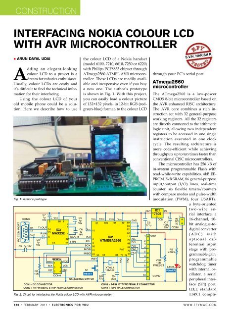
Fig. 1: Author’s prototype<br />
Fig. 2: Circuit for interfacing the Nokia <strong>colour</strong> LCD with avr microcontroller<br />
the <strong>colour</strong> LCD of a Nokia handset<br />
(model 6100, 7210, 6610, 7250 or 6220)<br />
with Philips PCF8833 chipset through<br />
ATmega2560 ATMEL AVR microcontroller.<br />
These LCDs are readily available<br />
and inexpensive even if you buy<br />
a new one. The author’s prototype<br />
is shown in Fig. 1. <strong>With</strong> this project,<br />
you can easily load a <strong>colour</strong> picture<br />
of 132×132 pixels, in 12-bit RGB (redgreen-blue)<br />
format, to the <strong>colour</strong> LCD<br />
s.v.n. harish k.<br />
through your PC’s serial port.<br />
ATmega2560<br />
microcontroller<br />
The ATmega2560 is a low-power<br />
CMOS 8-bit microcontroller based on<br />
the AVR enhanced RISC architecture.<br />
The AVR core combines a rich instruction<br />
set with 32 general-purpose<br />
working registers. All the 32 registers<br />
are directly connected to the arithmetic<br />
logic unit, allowing two independent<br />
registers to be accessed in one single<br />
instruction executed in one clock<br />
cycle. The resulting architecture is<br />
more code-efficient while achieving<br />
throughputs up to ten times faster than<br />
conventional CISC microcontrollers.<br />
The microcontroller has 256 kB of<br />
in-system programmable Flash with<br />
read-while-write capabilities, 4kB EE-<br />
PROM, 8kB SRAM, 86 general-purpose<br />
input/output (I/O) lines, real-time<br />
counter, six flexible timers/counters<br />
with compare modes and pulse-width<br />
modulation (PWM), four USARTs,<br />
a byte-oriented<br />
two-wire serial<br />
interface, a<br />
16-channel, 10-<br />
bit analogue-todigital<br />
converter<br />
(ADC) with<br />
optional differential<br />
input<br />
stage with programmable<br />
gain,<br />
programmable<br />
watchdog timer<br />
with internal oscillator,<br />
a serial<br />
peripheral interface<br />
(SPI) port,<br />
IEEE standard<br />
1149.1 compli-<br />
120 • February 2011 • electronics for you www.efymag.com
Construction<br />
Fig. 3: Front view of Nokia LCD with pin details<br />
of the connector<br />
Fig. 4: Circuit for Nokia lcd connector extension<br />
ant JTAG test interface (also used for<br />
accessing the on-chip debug system<br />
and programming) and six softwareselectable<br />
power-saving modes.<br />
PCF8833 LCD driver<br />
Fig. 5: Standard 12-bit image<br />
Fig. 6: GUI created using VB.net for image<br />
transfer from the PC<br />
The PCF8833 is a single-chip, lowpower<br />
CMOS LCD controller driver,<br />
designed to drive <strong>colour</strong> super-twisted<br />
nematic displays of 132 rows and 132<br />
RGB columns. All the necessary functions<br />
for the display are provided in a<br />
single chip, including the display RAM<br />
which has a capacity of 209 kbits. The<br />
PCF8833 uses multiple-row addressing<br />
technique in order to achieve the<br />
best optimal performance at the lowest<br />
power consumption. It offers two types<br />
of microcontroller interfaces: 8080 system<br />
interface and 3-line serial interface.<br />
The PCF8833 communicates with<br />
the host using an 8-bit parallel interface<br />
or 3-line serial interface. Here a<br />
3-line serial interface is implemented<br />
for communication between the microcontroller<br />
and the PCF8833 chip.<br />
The three lines are chip-select (CS) or<br />
enable pin, serial clock (SCLK) and serial<br />
data (SD).<br />
Processing the instructions and<br />
data sent to the interface does not<br />
require the display clock. The display<br />
clock and interface clock are independent<br />
of each other. The display clock is<br />
derived from the built-in oscillator.<br />
The serial data pin of PCF8833 is connected<br />
to the SDA pin of the microcontroller.<br />
Circuit description<br />
Fig. 2 shows the circuit for interfacing<br />
the Nokia <strong>colour</strong> LCD with Atmega2560<br />
microcontroller. The circuit<br />
is powered from a standard 9V DC<br />
source. The 9V DC is converted into 5V<br />
DC using a 7805 regulator (IC1). The<br />
glowing of LED1 shows the presence<br />
of power in the circuit. The regulated<br />
5V supply powers the circuit including<br />
the Atmega2560, MAX232, LCD<br />
connector (CON2) and ISP6 connector<br />
(CON4). CON3 is a 9-pin, D-type<br />
COM port connector used to interface<br />
with the PC for picture file transfer to<br />
the LCD through the microcontroller<br />
(IC2). ISP6 connector is used for programming<br />
the microcontroller using<br />
STK500 board.<br />
Whenever the program<br />
doesn’t function properly,<br />
you can reset the microcontroller<br />
by momentarily<br />
pressing reset switch S1.<br />
Pin details of Nokia’s 10-pin LCD<br />
connector are shown in Fig. 3. A manual<br />
implementation of the SPI with the<br />
microcontroller is done through SDA,<br />
CLK and CS pins on the LCD connector.<br />
First, the clock pin is cleared, then<br />
the data pin is set or cleared depending<br />
on the data bit and the clock pin set.<br />
SDA and CLK pins of the LCD connector<br />
are connected to pins 77 (PA1)<br />
and 76 (PA2) of the microcontroller,<br />
respectively.<br />
The 8-bit data is transferred<br />
through the SPI in eight clock cycles.<br />
CS pin of the LCD chip is permanently<br />
made low. Backlight LED pin for the<br />
LCD may be connected to a PWM pin<br />
to have a dimming effect depending on<br />
the duty cycle of PWM.<br />
The LED and Reset pins of the LCD<br />
are connected to pins 75 (PA3) and 78<br />
(PA0) of the microcontroller, respectively.<br />
When PA0 is made low, it resets<br />
the LCD. All the lines PA0 to PA3 is<br />
made an output pin by setting the data<br />
direction register (DDRA) bits high.<br />
This connector is too small to handle<br />
and solder using a normal soldering<br />
iron. You can extend the connections<br />
to a standard-size berg strip male connector<br />
as shown in Fig. 4. The LCD<br />
connector extension may be developed<br />
with resistors R3 through R5 (1<br />
kilo-ohm each) and R6 through R8 (2.2<br />
kilo-ohms each) forming the voltage<br />
divider circuits to obtain 3.3V signals<br />
(acceptable by the <strong>colour</strong> LCD) from<br />
5.5V TTL signals.<br />
Note that this connector extension<br />
is made for use with a <strong>colour</strong> LCD as<br />
well as standard character LCD. The<br />
LCD receives 3.3V supply through preset<br />
VR1. VR1 is also used to adjust the<br />
brightness of the <strong>colour</strong> LCD. Contrast<br />
is adjusted through software program.<br />
Make a PCB layout and glue the<br />
board on the back side of the LCD<br />
module. Now you can easily fit the<br />
LCD onto the 10-pin berg strip socket<br />
www.efymag.com<br />
electronics for you • February 2011 • 121
cONSTRUCTION<br />
Fig. 7: An actual-size, single-side PCB for interfacing the Nokia <strong>colour</strong> LCD with the AVR<br />
microcontroller circuit<br />
Parts List<br />
Semiconductors:<br />
IC1<br />
- 7805, 5V regulator<br />
IC2<br />
- ATmega2560 microcontroller<br />
IC3<br />
- MAX232 RS-232 driver<br />
LED1 - 5mm light-emitting diode<br />
Resistors (all ¼-watt, ±5% carbon):<br />
R1<br />
- 10-kilo-ohm<br />
R2<br />
- 470-ohm<br />
R3-R5 - 1-kilo-ohm<br />
R6-R8 - 2.2-kilo-ohm<br />
VR1 - 10-kilo-ohm preset<br />
Capacitors:<br />
C1<br />
- 100µF, 25V electrolytic<br />
C2<br />
- 0.1µF ceramic<br />
C3, C4 - 22pF ceramic<br />
C5-C8 - 1µF, 16V electrolytic<br />
C9<br />
- 10µF, 16V electrolytic<br />
Miscellaneous:<br />
CON1 - DC connector<br />
CON2 - 10-pin berg strip female<br />
connector<br />
CON3 - 9-pin D-type female<br />
connector<br />
CON4 - ISP 6-pin male connector<br />
CON5 - 10-pin berg strip male<br />
connector<br />
CON6 - 10-pin connector for<br />
Nokia LCD<br />
S1<br />
- Tactile switch<br />
- Nokia 6100 <strong>colour</strong> LCD<br />
module<br />
Fig. 8: Component layout for the PCB in Fig. 7<br />
in your ATmega2560 application<br />
board.<br />
Software program<br />
The software for the microcontroller is<br />
written in ‘C’ language using the IAR<br />
Embedded Workbench integrated development<br />
environment. IAR Embedded<br />
Workbench is being developed by<br />
IAR Systems and ATMEL developers<br />
in parallel and hence it generates the<br />
optimised code which uses full ‘C’<br />
coding capabilities of AVR devices.<br />
AVR development tools for embedded<br />
systems can be downloaded for free<br />
from IAR website www.iar.com. For<br />
details of IAR Embedded Workbench,<br />
you may refer to ‘A Beginners’ Guide<br />
to ATMEL AVR Development’ article<br />
published in January issue of EFY.<br />
To start the application, click ‘IAR<br />
Embedded Workbench’ icon in ‘All<br />
Programs’ menu of Windows. From<br />
the main menu, select Project→Create<br />
New Project and start an AVR Studio<br />
compatible C project. Generate the<br />
Intel hex file for burning the code into<br />
Atmega2560 microcontroller as follows:<br />
Project→Options→Linker (under<br />
Category)→Extra Output→Generate<br />
Extra Output (to click)→Override<br />
Default (to click)→Type Project Name.<br />
hex→Output Format→intel-standard<br />
(to select).<br />
Press ‘ok’ after all these settings are<br />
done. The source code for LCD interfacing<br />
(main.c) along with comments<br />
for instructions is included in this<br />
month’s EFY-CD. Import the main.c<br />
file from the CD into the editor screen<br />
by clicking ‘Add Files...’ option in Project<br />
menu. Click ‘Compile’ option from<br />
Project menu to compile and generate<br />
main.hex code.<br />
To send a command, a low bit is<br />
sent first before sending an 8-bit command,<br />
forming a 9-bit SPI command<br />
signal. Similarly, before sending an<br />
8-bit data, a high bit is sent forming<br />
a 9-bit SPI data. You may refer to<br />
the datasheet of PCF8833 for various<br />
instructions used in the LCD driver<br />
chip. The code for this project (main.c)<br />
has been programmed as per these<br />
instructions.<br />
If you can draw a point with a <strong>colour</strong><br />
at any given location on the LCD<br />
screen, you can implement various<br />
graphics algorithms to draw a circle,<br />
line, filled rectangle, etc. You can have<br />
the AVR microcontroller fitted with a<br />
16.00MHz external crystal oscillator, a<br />
serial RS-232 driver connecting a serial<br />
port and a reset arrangement to run<br />
the code.<br />
Downloading the code into Atmega2560.<br />
To program the Atmega2560,<br />
connect the 6-wire cable between<br />
ISP connectors of the STK500 board<br />
(marked as ISP6) and the target board<br />
(marked as ISP con). Connect a serial<br />
cable from ‘RS232 CTRL’ connector<br />
on the STK500 board to a COM port<br />
on the PC. Now start AVR Studio 4.0<br />
without opening any project file.<br />
Optionally, you may proceed as<br />
follows: Main Menu→Tools→Program<br />
122 • February 2011 • electronics for you www.efymag.com
Construction<br />
Fig. 9: An actual-size, single-side PCB for the<br />
LCD extension circuit<br />
AVR→Select AVR Programmer. Press<br />
‘Connect...’ after selecting STK500 or<br />
AVRISP in the platform window and<br />
COM port (say, COM1) in the port<br />
window. Next, select Atmega2560 as<br />
‘Device,’ ISP as ‘Programming Mode’<br />
and browse your project hex file from<br />
Project→Debug→Exe folder. Press<br />
‘Program’ button on the STK500 dialogue<br />
box to burn the hex file into your<br />
microcontroller.<br />
Converting the image file. You may<br />
convert any image file into a .raw file<br />
of 132×132 size, in 12-bit RGB <strong>colour</strong>,<br />
using Adobe Photoshop.<br />
A standard 12-bit image encodes<br />
the two pixels in three bytes of data<br />
(24 bits) as shown in Fig. 5. In a 12-bit<br />
image, each pixel has three <strong>colour</strong> components<br />
of 4-bit value (0 to 15). So each<br />
of red, green and blue can vary from<br />
0 to 15. Now, as a single COM port<br />
communication or any serial communication<br />
has 8-bit data and 12 bits are<br />
one-and-a-half byte, the two pixels are<br />
transferred so that 12×2 = 24-bit value<br />
is sent in three successive transfers of<br />
8-bit value. Same is the case when storing<br />
these pixels in a file or a memory<br />
which stores a byte value only. The<br />
two pixels having 24 bits can be stored<br />
in three bytes of data.<br />
A front-end (user-interface) program<br />
for transferring a picture file to<br />
the AVR microcontroller may be designed<br />
using a suitable software.<br />
Using GUI to transfer the image.<br />
Fig. 10: Component layout for the PCB in Fig. 9<br />
The user-interface program for transferring<br />
the picture file (.raw) from your<br />
PC to the Nokia LCD is designed in<br />
Visual Basic.NET platform. The send_<br />
picture.exe file is already included in<br />
the EFY-CD of this issue. When you<br />
click this file, you will see a GUI window<br />
as shown in Fig. 6.<br />
In the first drop-down menu, select<br />
the appropriate com port. The image<br />
to be transferred should be saved in<br />
*.raw format. Select that image using<br />
‘Browse’ option in the second pane<br />
and press ‘Send’ button to transfer the<br />
image to the graphical LCD. Now the<br />
image is displayed on the LCD.<br />
Writing a text to the screen is similar<br />
to drawing a bitmap with predefined<br />
height, width and <strong>colour</strong> of characters.<br />
Construction<br />
An actual-size, single-side PCB for<br />
interfacing the Nokia <strong>colour</strong> LCD with<br />
the AVR microcontroller circuit (Fig.<br />
2) is shown in Fig. 7 and its component<br />
layout in Fig. 8. An actual-size, singleside<br />
PCB for the LCD extension circuit<br />
(Fig. 4) is shown in Fig. 9 and its component<br />
layout in Fig. 10.<br />
Mount all the components as<br />
shown in the PCB layouts. The Atmega2560<br />
used in the prototype comes in<br />
a 100-pin, surface-mount TQFP package.<br />
By using surface-mount devices<br />
(SMDs) in your project, you don’t have<br />
to drill holes in the PCB and the board<br />
size will be much smaller. But it may<br />
be difficult to handle and solder SMDs<br />
without an SMD soldering station.<br />
However, with a normal soldering<br />
iron, tweezers and some basic knowledge,<br />
you can solder SMD components<br />
without much problem. You need<br />
good eyes, a steady hand and a soldering<br />
iron with a small, clean tip.<br />
Make sure that the PCB is clean.<br />
You may use copper polish material to<br />
remove all kinds of oxidation and acetone<br />
(nail polish remover) to remove<br />
all kinds of contaminations on the PCB.<br />
On the PCB, figure out the correct<br />
location for placing the SMDs.<br />
Fixate the SMD at the top right<br />
corner and the bottom left corner.<br />
Carefully solder SMD pins one by one.<br />
SMD components are very sensitive to<br />
heat, so allow your SMD to cool down<br />
after every step. For more tips on soldering<br />
SMD components, you may refer to<br />
http://hem.passagen.se/communication/pcbsmd.html<br />
and www.engadget.<br />
com/2006/03/07/how-to-make-asurface-mount-soldering-iron/<br />
websites.<br />
After soldering the components<br />
on the PCBs, insert the LCD connector<br />
extension board in the main interfacing<br />
PCB using the connector marked<br />
‘CON2.’ <strong>With</strong> the LCD screen facing towards<br />
you, the leftmost pin of the berg<br />
strip is pin 1. Make sure that the orientation<br />
of the LCD connector is correct.<br />
Now connect 9V DC source to the<br />
circuit and switch on the power supply.<br />
LED1 should glow to indicate the<br />
presence of power in the circuit. At<br />
this point, you will see a test <strong>colour</strong><br />
band drawn by itself on the LCD<br />
screen and then waits for serial port<br />
to get 12-bit RGB image from PC at<br />
115.2 kbps baud rate. Now run the<br />
send_picture.exe file and send the<br />
picture file (.raw) to the LCD from<br />
your computer.<br />
EFY note. The source codes of this<br />
article (main.c and Visual Basic.net<br />
GUI program) have been included<br />
in this month’s EFY-CD and are also<br />
available on efymag.com website. •<br />
The author is an assistant professor in Department<br />
of Mechanical Engineering at Birla Institute of<br />
Technology, Mesra, Ranchi<br />
www.efymag.com<br />
electronics for you • February 2011 • 123