AVr ProgrAMMer using AVr910 Protocol SUNIL KUMAR
AVr ProgrAMMer using AVr910 Protocol SUNIL KUMAR
AVr ProgrAMMer using AVr910 Protocol SUNIL KUMAR

Create successful ePaper yourself
Turn your PDF publications into a flip-book with our unique Google optimized e-Paper software.
cONSTRUCTION<br />
AVR Programmer<br />
Using AVR910 <strong>Protocol</strong><br />
sunil kumar<br />
• Arun Dayal Udai, Brij Mohan<br />
Newbies often have difficulty<br />
getting started with programming<br />
of AVR microcontroller<br />
memory. What they need is a simple<br />
documentation and the entire code for<br />
AVR memory programming.<br />
This article attempts to simplify the<br />
existing AVR910 technical note available<br />
on ATMEL’s website. It includes a<br />
source program for the microcontroller<br />
written in ‘C’ language for easy understanding<br />
of the principles and a user<br />
interface software program written in<br />
Microsoft Visual Basic .Net for interfacing<br />
and transferring a binary code to<br />
the target device.<br />
The complete system for programming<br />
an AVR microcontroller uses a<br />
universal asynchronous receiver transmitter<br />
(UART) with serial peripheral<br />
interface (SPI) to program the target<br />
microcontroller’s fuses, lock bits, flash<br />
or EEPROM. Any AVR board can be<br />
converted into a master programmer<br />
<strong>using</strong> this protocol.<br />
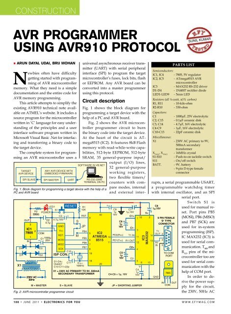
Circuit description<br />
Fig. 1: Block diagram for programming a target device with the help of a<br />
PC and AVR board<br />
Fig. 2: AVR microcontroller programmer circuit<br />
Parts List<br />
Semiconductors:<br />
IC1, IC4 - 7805, 5V regulator<br />
IC2, IC5 - ATmega8515 AVR<br />
microcontroller<br />
IC3<br />
- MAX232 RS-232 driver<br />
D1-D4 - 1N4007 rectifier diode<br />
LED1-LED9 - 5mm LED<br />
Resistors (all ¼-watt, ±5% carbon)<br />
R1, R11 - 10-kilo-ohm<br />
R2-R10 - 330-ohm<br />
Capacitors:<br />
C1<br />
- 1000µF, 25V electrolytic<br />
C2, C15 - 0.1µF ceramic disk<br />
C3, C14 - 4.7µF, 16V electrolytic<br />
C4-C9 - 1µF, 16V electrolytic<br />
C10-C13 - 22pF ceramic disk<br />
Miscellaneous:<br />
X1 - 230V AC primary to 9V,<br />
500mA secondary<br />
transformer<br />
X TAL1<br />
, X TAL2<br />
- 16MHz crystal<br />
S1-S10 - Push-to-on tacktile switch<br />
S11<br />
- On/off switch<br />
Batt. - 9V, battery<br />
- 9-pin D-type female<br />
connector<br />
Fig. 1 shows the block diagram for<br />
programming a target device with the<br />
help of a PC and AVR board.<br />
Fig. 2 shows the AVR microcontroller<br />
programmer circuit to burn<br />
the binary code into the target device.<br />
At the heart of the circuit is ATmega8515<br />
(IC2). It features 8kB Flash<br />
memory with read-while-write capabilities,<br />
512-byte EEPROM, 512-byte<br />
SRAM, 35 general-purpose input/<br />
output (I/O) lines,<br />
32 general-purpose<br />
working registers,<br />
two flexible timers/<br />
counters with compare<br />
modes, internal<br />
and external interrupts,<br />
a serial programmable USART,<br />
a programmable watchdog timer<br />
with internal oscillator, and an SPI<br />
serial port.<br />
Switch S1 is<br />
used for manual reset.<br />
Port pins PB5<br />
(MOSI), PB6 (MISO)<br />
and PB7 (SCK) are<br />
used for in-system<br />
programming (ISP).<br />
IC MAX232 (IC3) is<br />
used for serial communication.<br />
T XD<br />
and<br />
R XD<br />
pins of the microcontroller<br />
too are<br />
used for serial communication<br />
with the<br />
help of COM port.<br />
In order to derive<br />
the power supply<br />
for the circuit,<br />
the 230V, 50Hz AC<br />
100 • June 2011 • electronics for you www.efymag.com
cONSTRUCTION<br />
Fig. 3: An actual-size, single-side PCB for the circuit of AVR programmer <strong>using</strong> AVR910 protocol<br />
(Fig. 2)<br />
Fig. 4: Component layout for the PCB<br />
mains is stepped down by transformer<br />
X1 to deliver a secondary output of<br />
9V, 500 mA. The transformer output is<br />
rectified by a full-wave rectifier comprising<br />
diodes D1 through D4, filtered<br />
by capacitor C1 and regulated by IC<br />
7805 (IC1). Capacitor C2 bypasses the<br />
ripples present in the regulated supply.<br />
LED1 acts as the power indicator<br />
and resistor R2 limits the current<br />
through LED1.<br />
An actual-size, single-side PCB for<br />
the circuit of AVR programmer <strong>using</strong><br />
AVR910 protocol (Fig. 2) is shown in<br />
Fig. 3 and its component layout in Fig.<br />
4. Assemble the circuit on a PCB to<br />
minimise time and assembly errors.<br />
Carefully assemble the components<br />
and double-check for any overlooked<br />
error.<br />
The target AVR microcontroller<br />
enters serial programming mode only<br />
when its reset pin is active-‘low’. Immediately<br />
after the reset pin becomes<br />
low, serial clock (SCK) pin is driven<br />
to zero by the programmer. The reset<br />
pin makes the device SPI slave and<br />
the target device ready to accept<br />
instructions from the programmer<br />
through MOSI (master out, serial<br />
data in) and MISO (master in, serial<br />
out) pins.<br />
The serial programming instruction<br />
set can be referred through any<br />
AVR datasheet. It can be implemented<br />
on any AVR board by just making the<br />
device at 19,200 baud rate for UART<br />
and selecting a proper pin on the<br />
master device which will make the<br />
reset pin of the slave device low, SPI<br />
slave select input PB4 (SS) pin being<br />
the most convenient one. Three-pin<br />
connectors are provided on the programmer<br />
board for burning the code<br />
into the programmer or the target<br />
microcontroller.<br />
To program the ATmega8515 on<br />
the programmer board, connect a<br />
6-wire cable between ISP connectors<br />
(marked as ISP6PIN) of the STK500<br />
board and the programmer board.<br />
Connect a serial cable from the connector<br />
marked as ‘RS232 CTRL’ on<br />
the STK500 board to COM port of the<br />
PC. Connect the reset pin (RST) of the<br />
ISP connector to reset pin 9 of ATmega8515<br />
microcontroller IC2 by shorting<br />
the jumper (JP).<br />
Now start AVR Studio 4.0 without<br />
opening any project file. Optionally,<br />
you may proceed as follows: Main<br />
menu→Tools→Program AVR→Select<br />
AVR Programmer. Press ‘Connect’ after<br />
selecting STK500 or AVRISP in the<br />
platform window and COM port (say,<br />
COM1) in the port window.<br />
After selection, ‘AVR Studio<br />
STK500 Programming Menu’ window<br />
appears. Select ‘ATmega8515’ as<br />
the device, ‘ISP’ as the programming<br />
mode and browse your project hex file<br />
(prog.hex) from Project→Debug→Exe<br />
folder.<br />
You may verify fuse bits showing<br />
the default setting. Now press ‘Program’<br />
button in ‘Program’ tab to burn<br />
the hex file into your microcontroller<br />
(IC1). Disconnect IC1 from the ISP<br />
cable. Now the programmer board is<br />
ready to burn the binary file into the<br />
target AVR microcontroller.<br />
Software<br />
The software (AVR910) for the microcontroller<br />
is written in ‘C’ <strong>using</strong><br />
the IAR Embedded Workbench integrated<br />
development environment.<br />
IAR Embedded Workbench is being<br />
developed by IAR Systems and<br />
ATMEL developers in parallel and<br />
hence it generates the optimised code<br />
which uses full ‘C’ coding capabilities<br />
of AVR devices. AVR development<br />
tools for embedded systems can be<br />
102 • June 2011 • electronics for you www.efymag.com
cONSTRUCTION<br />
Table I<br />
SPI Command Sets (in Hex Format) for Serial Programming<br />
of the Target AVR Microcontroller*<br />
Instruction/operation<br />
downloaded for free from IAR website<br />
www.iar.com. For details of IAR<br />
Embedded Workbench, you may refer<br />
to ‘A Beginners’ Guide to ATMEL<br />
AVR Development’ article published<br />
in January issue of EFY.<br />
Coding for AVR programmer.<br />
When writing serial data to the AVR<br />
microcontroller, data is clocked on the<br />
rising edge of SCK. When reading data<br />
from the AVR microcontroller, data is<br />
clocked on the falling edge of SCK. To<br />
program and verify the AVR microcontroller<br />
in the SPI serial programming<br />
mode, the following sequence is<br />
recommended (refer Table I for serial<br />
SPI instruction format<br />
byte 1 Byte 2 Byte 3 byte 4<br />
Programming Enable AC 53 00 00<br />
Chip Erase (program memory/<br />
EEPROM) AC 80 00 00<br />
Poll RDY/BSY F0 00 00 data byte out<br />
Load instructions<br />
Load extended address byte 4D 00 Extended adr 00<br />
Load program memory page,<br />
high byte 48 adr MSB adr LSB high data byte in<br />
Load program memory page,<br />
low byte 40 adr MSB adr LSB low data byte in<br />
Load EEPROM memory page<br />
(page access) C1 00 adr LSB data byte in<br />
Read instructions<br />
Read program memory, high byte 28 adr MSB adr LSB high data byte out<br />
Read program memory, low byte 20 adr MSB adr LSB low data byte out<br />
Read EEPROM memory A0 adr MSB adr LSB data byte out<br />
Read lock bits 58 00 00 data byte out<br />
Read signature byte 30 00 0000 000aa data byte out<br />
Read fuse bits 50 00 00 data byte out<br />
Read fuse high bits 58 08 00 data byte out<br />
Read extended fuse bits 50 08 00 data byte out<br />
Read calibration byte 38 00 0b00 000bb data byte out<br />
Write instructions<br />
Write program memory page 4C 000a aaaa aa00 0000 00<br />
Write EEPROM memory C0 adr MSB adr LSB data byte in<br />
Write EEPROM memory page<br />
(page access) C2 adr MSB adr LSB 00<br />
Write lock bits AC E0 00 data byte in<br />
Write fuse bits AC A0 00 data byte in<br />
Write fuse high bits AC A8 00 data byte in<br />
Write extended fuse bits AC A4 00 data byte in<br />
*Commands are sent by the programmer board to the slave device which is being programmed<br />
programming command):<br />
1. Power-up: Apply power between<br />
V CC<br />
and ground (GND) while<br />
Fig. 5: Burning the hex code into the programmer board<br />
microcontroller<br />
RST and SCK are set to ‘0’. In some<br />
systems, the programmer cannot<br />
guarantee that SCK is held low during<br />
power-up. In this case, RST must be<br />
given a positive pulse of at least two<br />
CPU clock cycles duration after SCK<br />
has been set to ‘0’.<br />
2. Wait for at least 20 ms and enable<br />
SPI serial programming by sending<br />
the ‘Programming Enable’ serial<br />
instruction to pin MOSI.<br />
3. The SPI serial programming<br />
instructions will not work if the communication<br />
is out of synchronisation.<br />
When in synchronisation, the<br />
second byte (0x53) will echo back<br />
when issuing the third byte of the<br />
‘Programming Enable’ instruction.<br />
Whether the echo is correct or not, all<br />
four bytes of the instruction must be<br />
transmitted. If the 0x53 doesn’t echo<br />
back, give a positive pulse to reset<br />
pin and issue a new ‘Programming<br />
Enable’ command.<br />
4. The Flash is programmed one<br />
page at a time. The memory page is<br />
loaded one byte at a time by supplying<br />
the six least significant bits (LSBs) of<br />
the address and data together with the<br />
“load program memory page” instruction.<br />
To ensure correct loading of the<br />
page, the low-byte data must be loaded<br />
before high-byte data is applied for a<br />
given address. The program memory<br />
page is stored by loading the “write<br />
program memory page” instruction<br />
with the seven most significant bits<br />
(MSBs) of the address. If polling is not<br />
used, the user must wait for a period<br />
of at least t WD_FLASH<br />
before issuing the<br />
next page. Accessing the SPI serial programming<br />
interface before<br />
completion of the<br />
Flash-write operation<br />
can result in incorrect<br />
programming.<br />
5. The EEPROM<br />
array is programmed<br />
one byte at a time by<br />
supplying the address<br />
and data together with<br />
the appropriate write<br />
instruction. An EE-<br />
PROM location is au-<br />
104 • June 2011 • electronics for you www.efymag.com
Construction<br />
Table II<br />
AVR910 UART Serial Commanding <strong>Protocol</strong><br />
Host PC writes<br />
Host PC reads<br />
ID Data ID Data<br />
Enter programming mode ‘P’ — — 13d<br />
Report auto increment address ‘a’ — — ‘Y’<br />
Set address ‘A’ ah al — 13d<br />
Write program memory, low byte ‘c’ Dd — 13d<br />
Write program memory, high byte ‘C’ Dd — 13d<br />
Issue page write ‘m’ — — 13d<br />
Read program memory ‘R’ — dd(dd) —<br />
Write data memory ‘D’ dd — 13d<br />
Read data memory ‘d’ — dd —<br />
Chip erase ‘e’ — — 13d<br />
Write lock bits ‘l’ dd — 13d<br />
Write fuse bits ‘f’ dd — 13d<br />
# Read fuse and lock bits ‘F’ — dd —<br />
Leave programming mode ‘L’ — — 13d<br />
Select device type ‘T’ dd — 13d<br />
Read signature bytes ‘s’ — 3*dd —<br />
Return supported device codes ‘t’ — n*dd 00d<br />
Return software identifier ‘S’ — s[7] —<br />
Return software version ‘V’ — dd dd —<br />
Return hardware version ‘v’ — dd dd —<br />
Return programmer type ‘p’ — dd —<br />
Set LED ‘x’ dd — 13d<br />
Clear LED ‘y’ dd — 13d<br />
Universal command ‘:’ 3*dd dd 13d<br />
New universal command ‘.’ 4*dd dd 13d<br />
Special test command ‘Z’ 2*dd dd —<br />
Fig. 6: VB.NET form layout for programmer software<br />
Fig. 7: Screenshot of raw binary file generation<br />
tomatically erased before new data<br />
is written. If polling is not used, the<br />
user must wait for a period of at least<br />
t WD_EEPROM<br />
before issuing the next byte.<br />
In a chip-erased device, no 0xFFs in<br />
the data files need to be programmed.<br />
6. Any memory location can be<br />
verified by <strong>using</strong> the read instruction,<br />
which returns the content at the selected<br />
address at serial output MISO.<br />
7. At the end of the programming<br />
session, RST can be set high to commence<br />
normal operation.<br />
8. Power-off (if needed): Set RST to<br />
‘1’ and turn V CC<br />
power off.<br />
Programming the target AVR microcontroller<br />
(for user interface) <strong>using</strong><br />
Visual Basic .NET (VB.NET). Once the<br />
master device (IC2) is ready to receive<br />
data or command from the PC and is<br />
connected to the slave device (IC5), it<br />
only requires an interface software on<br />
the PC which can supply data/command<br />
to it. This<br />
interface software<br />
is written in Visual<br />
Basic .NET. It supports<br />
AVR910 insystem<br />
programming<br />
protocol for<br />
commands. The<br />
interface software<br />
(ADU-ISP) given<br />
here can implement<br />
almost all ATmega AVR microcontrollers<br />
having Flash size of less<br />
than 128 kB. Just construct a form in<br />
VB which has the controls as shown<br />
in Fig. 6, with SerialPort and OpenFileDialog<br />
controls, and insert the code<br />
that follows.<br />
The source program includes remarks<br />
for easy understanding.<br />
Table II shows AVR910 UART<br />
serial commanding protocol. These<br />
commands are sent to the programmer<br />
board through serial communication<br />
<strong>using</strong> the VB.NET program.<br />
All commands comprise a single<br />
letter. The programmer returns 13d,<br />
which is a carriage-return character<br />
or the data read after the command<br />
is finished.<br />
The VB.NET program accepts raw<br />
binary file (*.bin) file, which is generated<br />
after compiling and linking a source<br />
program for the microcontroller. This<br />
binary file data has to be burnt into the<br />
www.efymag.com<br />
electronics for you • June 2011 • 105
cONSTRUCTION<br />
target AVR microcontroller.<br />
Currently, all the ATmega AVR<br />
microcontroller devices, except ATmega640/1280/1281/2560/2561,<br />
have<br />
Flash size of up to 128 kB. Writing<br />
(burning the code into) the Flash of<br />
ATmega640/1280/1281/2560/2561<br />
requires extended addresses. Also, as<br />
these devices have a higher pin count<br />
and come in TQFP package, they will<br />
not fit into the programmer board<br />
described here. This AVR programmer<br />
works fine with ATmega8515 and<br />
ATmega16/32.<br />
If the user is programming <strong>using</strong><br />
IAR Embedded Workbench, the steps<br />
for generating a raw binary file (*.bin)<br />
file are:<br />
Goto Project→Options→Linker→<br />
Extra Output→Tick ‘Generate Extra<br />
Output File’→Tick ‘Override<br />
Default’→Select ‘Output Format’ as<br />
‘Raw-Binary’ (refer Fig. 7).<br />
A VB.net program writes the<br />
raw binary file starting from address<br />
‘0000’ of the flash memory. So when<br />
writing a code which does not start<br />
from ‘0000’ address, the user needs<br />
to take care by editing the linker<br />
(*.xcl) file before compiling the AVR<br />
Fig. 8: LED switching circuit<br />
source code.<br />
A sample code for LED switching<br />
(led_sw.c) is given at the end of<br />
this article to test the working of the<br />
AVR programmer board. This code<br />
has to be burnt into the target device.<br />
Eight LEDs are connected to Port C<br />
led_sw.c<br />
of the microcontroller<br />
(IC5)<br />
with their controlling<br />
switches<br />
connected to<br />
Port A. Initially,<br />
when IC5 is<br />
programmed<br />
successfully,<br />
all the LEDs<br />
glow. Now if<br />
you press any<br />
of the switches,<br />
the corresponding<br />
LED<br />
should go off.<br />
Fig. 8 shows<br />
the circuit<br />
for LED<br />
switching.<br />
E F Y<br />
note. The<br />
source codes<br />
AVR910.C, LED_SW.C and ADU_ISP<br />
are available on www.efymag.com<br />
website.<br />
Arun Dayal Udai is an assistant professor in<br />
Department of Mechanical Engineering at Birla<br />
Institute of Technology, Mesra, and Brij Mohan is<br />
a project leader at Mphasis Ltd, Bengaluru<br />
/* led_sw.c*/<br />
#include <br />
#include <br />
#define LED0 PORTC0 //Connected to PORTC<br />
#define LED1 PORTC1 //Connected to PORTC<br />
#define LED2 PORTC2 //Connected to PORTC<br />
#define LED3 PORTC3 //Connected to PORTC<br />
#define LED4 PORTC4 //Connected to PORTC<br />
#define LED5 PORTC5 //Connected to PORTC<br />
#define LED6 PORTC6 //Connected to PORTC<br />
#define LED7 PORTC7 //Connected to PORTC<br />
#define SW0 PINA0<br />
#define SW1 PINA1<br />
are connected to PORTA<br />
#define SW2 PINA2<br />
#define SW3 PINA3<br />
#define SW4 PINA4<br />
#define SW5 PINA5<br />
#define SW6 PINA6<br />
#define SW7 PINA7<br />
//All Switches<br />
#define SETBIT(ADDRESS, BIT) (ADDRESS<br />
|= (1