A custom front-end ASIC for the readout and timing of 64 SiPM ...
A custom front-end ASIC for the readout and timing of 64 SiPM ...
A custom front-end ASIC for the readout and timing of 64 SiPM ...

Create successful ePaper yourself
Turn your PDF publications into a flip-book with our unique Google optimized e-Paper software.
Nuclear Physics B (Proc. Suppl.) 215 (2011) 344–348<br />
www.elsevier.com/locate/npbps<br />
A <strong>custom</strong> <strong>front</strong>-<strong>end</strong> <strong>ASIC</strong> <strong>for</strong> <strong>the</strong> <strong>readout</strong> <strong>and</strong> <strong>timing</strong> <strong>of</strong> <strong>64</strong> <strong>SiPM</strong><br />
photosensors<br />
M.G. Bagliesi a∗ ,C.Avanzini b , G. Bigongiari a , R. Cecchi a ,M.Y.Kim a ,P.Maestro a , P.S. Marrocchesi a ,<br />
F. Morsani b<br />
a Department <strong>of</strong> Physics, University <strong>of</strong> Siena <strong>and</strong> INFN, Via Roma 56, 53100 Siena, Italy<br />
b INFN Sezione di Pisa, Edificio C-Polo Fibonacci Largo Bruno Pontecorvo 3, 56127 Pisa, Italy<br />
A new class <strong>of</strong> instruments – based on Silicon PhotoMultiplier (<strong>SiPM</strong>) photosensors – are currently under<br />
development <strong>for</strong> <strong>the</strong> next generation <strong>of</strong> Astroparticle Physics experiments in future space missions. A <strong>custom</strong><br />
<strong>front</strong>-<strong>end</strong> <strong>ASIC</strong> (Application Specific Integrated Circuit) <strong>for</strong> <strong>the</strong> <strong>readout</strong> <strong>of</strong> <strong>64</strong> <strong>SiPM</strong> sensors was specified in<br />
collaboration with GM-IDEAS (Norway) that designed <strong>and</strong> manufactured <strong>the</strong> <strong>ASIC</strong>. Our group developed a<br />
<strong>custom</strong> <strong>readout</strong> board equipped with a 16 bit ADC <strong>for</strong> <strong>the</strong> digitization <strong>of</strong> both pulse height <strong>and</strong> time in<strong>for</strong>mation.<br />
A time stamp, generated by <strong>the</strong> <strong>ASIC</strong> in correspondence <strong>of</strong> <strong>the</strong> threshold crossing time, is digitized <strong>and</strong> recorded<br />
<strong>for</strong> each channel. This allows to define a narrow time window around <strong>the</strong> physics event that reduces significantly<br />
<strong>the</strong> background due to <strong>the</strong> <strong>SiPM</strong> dark count rate. In this paper, we report on <strong>the</strong> preliminary test results obtained<br />
with <strong>the</strong> <strong>readout</strong> board prototype.<br />
1. INTRODUCTION<br />
In <strong>the</strong> recent years, <strong>the</strong> introduction <strong>of</strong> <strong>the</strong> Silicon<br />
PhotoMultiplier (<strong>SiPM</strong>) – a new solid-state<br />
photosensor operating in quenched Geiger mode<br />
[1–5] – has been followed by an intense work <strong>of</strong><br />
research <strong>and</strong> development worldwide, leading to<br />
significant advances in this field as in <strong>the</strong> case <strong>of</strong><br />
<strong>the</strong> Digital <strong>SiPM</strong> concept [6]. The application <strong>of</strong><br />
<strong>SiPM</strong> photosensors as a potential replacement <strong>of</strong><br />
traditional photomultipliers spans many different<br />
detection techniques in particle physics.<br />
In this paper, we focus on <strong>the</strong> impact <strong>of</strong> this new<br />
device in <strong>the</strong> detection <strong>of</strong> Cherenkov light, a field<br />
that may require <strong>the</strong> capability to deal with very<br />
low light levels. Differential Cherenkov detectors<br />
– as <strong>the</strong> Ring Imaging Cherenkov (RICH) or<br />
<strong>the</strong> Detection <strong>of</strong> Internally Reflected Cherenkov<br />
Light (DIRC) – are based on <strong>the</strong> imaging <strong>of</strong> specific<br />
patterns <strong>of</strong> Cherenkov light, generated by<br />
<strong>the</strong> passage <strong>of</strong> a charged particle through a radiator,<br />
onto a detection plane structured into cells<br />
or pixels. For particles carrying one unit <strong>of</strong> electric<br />
charge (Z=1), <strong>the</strong> number <strong>of</strong> photons hitting<br />
a single pixel can fluctuate around a quite small<br />
∗ mg.bagliesi@pi.infn.it<br />
average value, thus requiring photosensors with<br />
single-photon detection capability.<br />
Arrays <strong>of</strong> <strong>SiPM</strong> devices, with a variety <strong>of</strong> different<br />
pixel sizes <strong>and</strong> covering sensitive areas <strong>of</strong> several<br />
tens <strong>of</strong> square millimeters, have been manufactured<br />
[7–10], but <strong>the</strong> typical dark count rates at<br />
room temperature (or with moderate cooling) are<br />
still too large to isolate <strong>the</strong> hits originated by <strong>the</strong><br />
Cherenkov emission from <strong>the</strong> background noise in<br />
<strong>the</strong> image.<br />
A way to circumvent this problem is to take advantage<br />
<strong>of</strong> <strong>the</strong> synchronous emission <strong>of</strong> photons<br />
radiated into <strong>the</strong> Cherenkov cone with respect to<br />
<strong>the</strong> r<strong>and</strong>om distribution <strong>of</strong> <strong>the</strong> <strong>SiPM</strong> dark counts<br />
in time. The need to record <strong>the</strong> arrival time <strong>of</strong><br />
each photon hitting <strong>the</strong> photodetector array, lead<br />
to <strong>the</strong> specifications <strong>for</strong> a new <strong>front</strong>-<strong>end</strong> <strong>ASIC</strong> capable<br />
<strong>of</strong> providing (in addition to a pulse height<br />
measurement) an accurate time-stamp <strong>for</strong> each<br />
<strong>SiPM</strong> <strong>readout</strong> channel. This feature allows to<br />
select pixels carrying useful in<strong>for</strong>mation on <strong>the</strong><br />
Cherenkov image within a narrow “time-window”<br />
relative to an external trigger or relying on <strong>the</strong><br />
self-triggering capabilities <strong>of</strong> <strong>the</strong> device. As a result<br />
<strong>of</strong> <strong>the</strong> application <strong>of</strong> <strong>the</strong> time filtering, <strong>the</strong><br />
contrast <strong>of</strong> <strong>the</strong> image can be improved providing<br />
0920-5632/$ – see <strong>front</strong> matter © 2011 Elsevier B.V. All rights reserved.<br />
doi:10.1016/j.nuclphysbps.2011.04.049
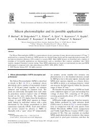
M.G. Bagliesi et al. / Nuclear Physics B (Proc. Suppl.) 215 (2011) 344–348 345<br />
Figure 1. Overview <strong>of</strong> <strong>the</strong> VATA<strong>64</strong>-HDR16 <strong>ASIC</strong>.<br />
a better efficiency to identify <strong>the</strong> Cherenkov pattern.<br />
In this paper, we briefly describe <strong>the</strong> main functionalities<br />
<strong>of</strong> <strong>the</strong> new <strong>ASIC</strong> <strong>and</strong> a few preliminary<br />
results obtained with our first prototype test<br />
board.<br />
2. VATA<strong>64</strong>-HDR16: a <strong>front</strong>-<strong>end</strong> <strong>ASIC</strong> <strong>for</strong><br />
<strong>SiPM</strong> <strong>readout</strong><br />
The VATA<strong>64</strong>-HDR16 is a <strong>64</strong> channel <strong>front</strong>-<strong>end</strong><br />
<strong>ASIC</strong> based on <strong>the</strong> VATA architecture (<strong>for</strong> a short<br />
review on <strong>the</strong> early history <strong>of</strong> <strong>ASIC</strong>s <strong>for</strong> High Energy<br />
Physics see <strong>for</strong> instance [11]) <strong>and</strong> tailored<br />
<strong>for</strong> <strong>SiPM</strong> read-out. It has been specified in collaboration<br />
with GM-IDEAS [12] that developed<br />
<strong>the</strong> <strong>ASIC</strong> under a 0.35μm CMOS manufacturing<br />
process with an epitaxial protection against SEE<br />
effects in space applications. An overview <strong>of</strong> <strong>the</strong><br />
<strong>ASIC</strong> can be found in Fig. 1.<br />
All <strong>the</strong> <strong>ASIC</strong> main operational parameters can<br />
be programmed by downloading a “slow control”<br />
configuration after power-up.<br />
The analog signal processing takes place in<br />
<strong>the</strong> <strong>front</strong>-<strong>end</strong> channels <strong>of</strong> <strong>the</strong> device, while <strong>the</strong><br />
read-out is h<strong>and</strong>led in <strong>the</strong> back-<strong>end</strong>. Each channel<br />
consists <strong>of</strong> a charge sensitive preamplifier, a<br />
fast shaper <strong>for</strong> triggering <strong>and</strong> <strong>timing</strong> <strong>and</strong> a slow<br />
shaper to provide a charge measurement. The<br />
output <strong>of</strong> <strong>the</strong> fast shaper is fed into a discriminator.<br />
The architecture <strong>of</strong> <strong>the</strong> channel <strong>readout</strong> is<br />
shown in Fig. 2.<br />
At power-on, a threshold can be set <strong>and</strong> individually<br />
adjusted <strong>for</strong> each cannel.<br />
In auto-trigger mode, whenever a channel exceeds<br />
its threshold value, <strong>the</strong> (auto-)trigger signal is asserted.<br />
The trigger can be output to <strong>the</strong> global<br />
<strong>of</strong>f-chip trigger line <strong>and</strong> may also be used to generate<br />
an on-chip Sample-<strong>and</strong>-Hold (SH) signal.<br />
A Time-To-Analogue-Converter (TAC) is implemented<br />
as a voltage ramp initiated by <strong>the</strong> trigger
346<br />
M.G. Bagliesi et al. / Nuclear Physics B (Proc. Suppl.) 215 (2011) 344–348<br />
Figure 2. Architecture <strong>of</strong> one <strong>front</strong>-<strong>end</strong> channel <strong>of</strong> <strong>the</strong> VATA<strong>64</strong>-HDR16 <strong>ASIC</strong>.<br />
<strong>and</strong> sampled with <strong>the</strong> SH signal. The slow shaper<br />
is followed by a Peak & Hold device.<br />
The outputs <strong>of</strong> all channels are <strong>readout</strong> via two<br />
multiplexers running in parallel, one <strong>for</strong> <strong>the</strong> sampled<br />
slow shaper charge measurement <strong>and</strong> one <strong>for</strong><br />
<strong>the</strong> TAC values. The output <strong>of</strong> both multiplexers<br />
is made available via differential output current<br />
buffers. The <strong>ASIC</strong> can be sampled in three different<br />
ways:<br />
characterized by a number <strong>of</strong> hits detected simultaneously.<br />
3. The VATA<strong>64</strong>-HDR16 test board<br />
We developed a dedicated test-board, <strong>the</strong> VAB-<br />
HDR16 (see Fig. 3), equipped with all <strong>the</strong> circuitry<br />
<strong>for</strong> signal conditioning, digitization <strong>and</strong><br />
<strong>readout</strong>. For <strong>the</strong> <strong>readout</strong> <strong>of</strong> <strong>the</strong> current output<br />
• external sampling: this is <strong>the</strong> traditional<br />
VA sampling method;<br />
• internally generated sampling based on an<br />
internal trigger: a SH signal is issued at a<br />
programmable time delay;<br />
• internally generated sampling based on an<br />
external trigger: <strong>the</strong> <strong>ASIC</strong> senses <strong>the</strong><br />
TA/TB lines to check if any o<strong>the</strong>r <strong>ASIC</strong><br />
has triggered. The SH signal is issued at<br />
a programmable time delay.<br />
With <strong>the</strong> <strong>ASIC</strong> in “self-triggering” mode, whenever<br />
a channel exceeds its threshold it starts a<br />
new time measurement that is stopped after a<br />
programmable delay by <strong>the</strong> SH signal. In this<br />
way, we can measure <strong>the</strong> time differences between<br />
<strong>the</strong> first triggering channel <strong>and</strong> <strong>the</strong> o<strong>the</strong>r channels<br />
that have been hit. This functionality allows to<br />
define an <strong>of</strong>fline ”time window” to select events<br />
Figure 3. The VATA-HDR16 test board.
M.G. Bagliesi et al. / Nuclear Physics B (Proc. Suppl.) 215 (2011) 344–348 347<br />
buffers <strong>of</strong> <strong>the</strong> <strong>ASIC</strong>, two stages are used: <strong>the</strong> first<br />
one is a voltage feedback amplifier <strong>for</strong> current-tovoltage<br />
conversion, while <strong>the</strong> second one consists<br />
<strong>of</strong> a fully differential input <strong>and</strong> differential output<br />
device.<br />
For <strong>the</strong> analog to digital conversion, we used a 16<br />
bits, 1 MSPS, fully differential ADC. All configuration,<br />
control <strong>and</strong> <strong>readout</strong> signals were generated<br />
by an Altera FPGA <strong>of</strong> <strong>the</strong> Cyclone II family:<br />
<strong>the</strong> EP2C8T144. Our test-board is equipped<br />
with an USB 2 interface with a PC to download<br />
<strong>the</strong> configuration bits <strong>of</strong> <strong>the</strong> VATA<strong>64</strong>-HDR16, to<br />
read/write registers <strong>and</strong> to <strong>readout</strong> <strong>the</strong> digitized<br />
data.<br />
4. Tests <strong>of</strong> <strong>the</strong> VATA<strong>64</strong>-HDR16 with <strong>the</strong><br />
VAB-HDR16<br />
We report here on <strong>the</strong> preliminary tests per<strong>for</strong>med<br />
in our lab to verify <strong>the</strong> functionality <strong>of</strong><br />
<strong>the</strong> board <strong>and</strong> <strong>the</strong> <strong>ASIC</strong>. All <strong>the</strong> measurements<br />
reported below – relative to <strong>the</strong> pulse height linearity<br />
<strong>and</strong> <strong>the</strong> time response <strong>of</strong> <strong>the</strong> <strong>ASIC</strong> – were<br />
per<strong>for</strong>med with no <strong>SiPM</strong> devices connected to<br />
<strong>the</strong> test board.<br />
Pulse height linearity tests were per<strong>for</strong>med injecting<br />
known values <strong>of</strong> charge into <strong>the</strong> <strong>ASIC</strong> input.<br />
The VATA<strong>64</strong>-HDR16 showed a linear response<br />
<strong>for</strong> charges up to 12 pC (Fig. 4). For<br />
larger charges, a saturation effect was observed.<br />
The pedestal rms width could be lowered to σ ∼<br />
1 fC with simple EMI reduction precautions by<br />
shielding <strong>the</strong> board.<br />
The result <strong>of</strong> a test on <strong>the</strong> linearity <strong>of</strong> <strong>the</strong> time<br />
measurement is reported in Fig. 5. The first triggering<br />
channel was set to produce a constant time<br />
output t max whose value was set via <strong>the</strong> programmable<br />
SH time delay. We injected charge in<br />
a second channel at various delays with respect to<br />
<strong>the</strong> first one: <strong>the</strong> generated time-stamp showed a<br />
good linearity up to several hundreds <strong>of</strong> nanoseconds.<br />
The width <strong>of</strong> <strong>the</strong> time pedestal was found to be<br />
around σ ∼ 4 ADC units, i.e. 160 ps. (Fig. 6).<br />
Figure 4. Measurement <strong>of</strong> <strong>the</strong> pulse height linearity<br />
<strong>of</strong> <strong>the</strong> <strong>ASIC</strong>.<br />
5. Conclusions<br />
The basic functionalities <strong>of</strong> a new <strong>ASIC</strong>, specifically<br />
designed <strong>for</strong> <strong>SiPM</strong> <strong>readout</strong>, were tested using<br />
a <strong>custom</strong> test board. In a following paper<br />
we will report on our measurements – both in<br />
<strong>the</strong> lab <strong>and</strong> at a dedicated beam test – with<br />
<strong>SiPM</strong> photodetectors connected to <strong>the</strong> <strong>ASIC</strong>. At<br />
present, we are integrating <strong>the</strong> new <strong>ASIC</strong> <strong>readout</strong><br />
into <strong>SiPM</strong>-based prototypes <strong>of</strong> RICH <strong>and</strong> DIRC<br />
Cherenkov detectors.<br />
Acknowledgments<br />
The authors would like to thank Altera Inc. <strong>for</strong><br />
supporting <strong>the</strong> project through <strong>the</strong> Altera University<br />
program. This work has been funded by<br />
<strong>the</strong> Istituto Nazionale di Fisica Nucleare (INFN)<br />
in Italy in cooperation with GM-Ideas.<br />
REFERENCES<br />
1. V. Saveliev, V. Golovin et al., Nucl. Instrum.<br />
Meth. A 442 (2000) 223
348<br />
M.G. Bagliesi et al. / Nuclear Physics B (Proc. Suppl.) 215 (2011) 344–348<br />
Figure 5. Measurement <strong>of</strong> <strong>the</strong> time linearity <strong>of</strong><br />
<strong>the</strong> <strong>ASIC</strong>. The anti-correlation shown in <strong>the</strong> figure<br />
is due to <strong>the</strong> <strong>of</strong>fset in <strong>the</strong> time-stamp <strong>of</strong> <strong>the</strong><br />
first trigger which occurs at t max<br />
2. P. Buzhan, B. Dolgoshein et al., Nucl. Instrum.<br />
Meth. A 504 (2003) 48-52<br />
3. V. Golovin et al., Nucl. Instrum. Meth. A 518<br />
(2004) 560-5<strong>64</strong><br />
4. N. Dinu et. al., Nucl. Instrum. Meth. A 572<br />
(2007) 422-426<br />
5. M. Danilov, Nucl. Instrum. Meth. A 604<br />
(2009) 183-189<br />
6. T. Frach, G. Prescher <strong>and</strong> C. Degenhardt,<br />
Silicon photomultiplier technology goes fullydigital,<br />
January 2010 Electronic Engineering<br />
Times Europe, (2010) 10-11<br />
7. C. Piemonte, et al., Recent developments on<br />
silicon photomultipliers produced at FBKirst,<br />
in: IEEE NSS MIC 2007 Conference<br />
Record, N41-2, (2007) 20892092<br />
8. G. Llosa et al., First PET Imaging Results<br />
with Continuous LYSO Crystals <strong>and</strong> Monolithic,<br />
<strong>64</strong>-Pixel <strong>SiPM</strong> Matrices, in: IEEE NSS<br />
MIC 2010 Conference Record, M19-70<br />
9. Hamamatsu Photonics K.K., documentation<br />
<strong>of</strong> <strong>the</strong> multi-pixel photon counter, available at<br />
http://jp.hamamatsu.com/<br />
Figure 6. A typical time pedestal <strong>of</strong> one channel<br />
<strong>of</strong> <strong>the</strong> board during charge injection tests.<br />
10. http://sensl.com/products/siliconphotomultipliers/spmmatrix/<br />
11. G. Hall, Recent progress in <strong>front</strong> <strong>end</strong> <strong>ASIC</strong>s<br />
<strong>for</strong> high-energy physics, Nucl. Instr. Meth. A<br />
541 (2005) 248-258<br />
12. IDEAS ASA, Norway, VATA<strong>64</strong>-HDR16 documentation