A custom front-end ASIC for the readout and timing of 64 SiPM ...
A custom front-end ASIC for the readout and timing of 64 SiPM ...
A custom front-end ASIC for the readout and timing of 64 SiPM ...

You also want an ePaper? Increase the reach of your titles
YUMPU automatically turns print PDFs into web optimized ePapers that Google loves.
Nuclear Physics B (Proc. Suppl.) 215 (2011) 344–348<br />
www.elsevier.com/locate/npbps<br />
A <strong>custom</strong> <strong>front</strong>-<strong>end</strong> <strong>ASIC</strong> <strong>for</strong> <strong>the</strong> <strong>readout</strong> <strong>and</strong> <strong>timing</strong> <strong>of</strong> <strong>64</strong> <strong>SiPM</strong><br />
photosensors<br />
M.G. Bagliesi a∗ ,C.Avanzini b , G. Bigongiari a , R. Cecchi a ,M.Y.Kim a ,P.Maestro a , P.S. Marrocchesi a ,<br />
F. Morsani b<br />
a Department <strong>of</strong> Physics, University <strong>of</strong> Siena <strong>and</strong> INFN, Via Roma 56, 53100 Siena, Italy<br />
b INFN Sezione di Pisa, Edificio C-Polo Fibonacci Largo Bruno Pontecorvo 3, 56127 Pisa, Italy<br />
A new class <strong>of</strong> instruments – based on Silicon PhotoMultiplier (<strong>SiPM</strong>) photosensors – are currently under<br />
development <strong>for</strong> <strong>the</strong> next generation <strong>of</strong> Astroparticle Physics experiments in future space missions. A <strong>custom</strong><br />
<strong>front</strong>-<strong>end</strong> <strong>ASIC</strong> (Application Specific Integrated Circuit) <strong>for</strong> <strong>the</strong> <strong>readout</strong> <strong>of</strong> <strong>64</strong> <strong>SiPM</strong> sensors was specified in<br />
collaboration with GM-IDEAS (Norway) that designed <strong>and</strong> manufactured <strong>the</strong> <strong>ASIC</strong>. Our group developed a<br />
<strong>custom</strong> <strong>readout</strong> board equipped with a 16 bit ADC <strong>for</strong> <strong>the</strong> digitization <strong>of</strong> both pulse height <strong>and</strong> time in<strong>for</strong>mation.<br />
A time stamp, generated by <strong>the</strong> <strong>ASIC</strong> in correspondence <strong>of</strong> <strong>the</strong> threshold crossing time, is digitized <strong>and</strong> recorded<br />
<strong>for</strong> each channel. This allows to define a narrow time window around <strong>the</strong> physics event that reduces significantly<br />
<strong>the</strong> background due to <strong>the</strong> <strong>SiPM</strong> dark count rate. In this paper, we report on <strong>the</strong> preliminary test results obtained<br />
with <strong>the</strong> <strong>readout</strong> board prototype.<br />
1. INTRODUCTION<br />
In <strong>the</strong> recent years, <strong>the</strong> introduction <strong>of</strong> <strong>the</strong> Silicon<br />
PhotoMultiplier (<strong>SiPM</strong>) – a new solid-state<br />
photosensor operating in quenched Geiger mode<br />
[1–5] – has been followed by an intense work <strong>of</strong><br />
research <strong>and</strong> development worldwide, leading to<br />
significant advances in this field as in <strong>the</strong> case <strong>of</strong><br />
<strong>the</strong> Digital <strong>SiPM</strong> concept [6]. The application <strong>of</strong><br />
<strong>SiPM</strong> photosensors as a potential replacement <strong>of</strong><br />
traditional photomultipliers spans many different<br />
detection techniques in particle physics.<br />
In this paper, we focus on <strong>the</strong> impact <strong>of</strong> this new<br />
device in <strong>the</strong> detection <strong>of</strong> Cherenkov light, a field<br />
that may require <strong>the</strong> capability to deal with very<br />
low light levels. Differential Cherenkov detectors<br />
– as <strong>the</strong> Ring Imaging Cherenkov (RICH) or<br />
<strong>the</strong> Detection <strong>of</strong> Internally Reflected Cherenkov<br />
Light (DIRC) – are based on <strong>the</strong> imaging <strong>of</strong> specific<br />
patterns <strong>of</strong> Cherenkov light, generated by<br />
<strong>the</strong> passage <strong>of</strong> a charged particle through a radiator,<br />
onto a detection plane structured into cells<br />
or pixels. For particles carrying one unit <strong>of</strong> electric<br />
charge (Z=1), <strong>the</strong> number <strong>of</strong> photons hitting<br />
a single pixel can fluctuate around a quite small<br />
∗ mg.bagliesi@pi.infn.it<br />
average value, thus requiring photosensors with<br />
single-photon detection capability.<br />
Arrays <strong>of</strong> <strong>SiPM</strong> devices, with a variety <strong>of</strong> different<br />
pixel sizes <strong>and</strong> covering sensitive areas <strong>of</strong> several<br />
tens <strong>of</strong> square millimeters, have been manufactured<br />
[7–10], but <strong>the</strong> typical dark count rates at<br />
room temperature (or with moderate cooling) are<br />
still too large to isolate <strong>the</strong> hits originated by <strong>the</strong><br />
Cherenkov emission from <strong>the</strong> background noise in<br />
<strong>the</strong> image.<br />
A way to circumvent this problem is to take advantage<br />
<strong>of</strong> <strong>the</strong> synchronous emission <strong>of</strong> photons<br />
radiated into <strong>the</strong> Cherenkov cone with respect to<br />
<strong>the</strong> r<strong>and</strong>om distribution <strong>of</strong> <strong>the</strong> <strong>SiPM</strong> dark counts<br />
in time. The need to record <strong>the</strong> arrival time <strong>of</strong><br />
each photon hitting <strong>the</strong> photodetector array, lead<br />
to <strong>the</strong> specifications <strong>for</strong> a new <strong>front</strong>-<strong>end</strong> <strong>ASIC</strong> capable<br />
<strong>of</strong> providing (in addition to a pulse height<br />
measurement) an accurate time-stamp <strong>for</strong> each<br />
<strong>SiPM</strong> <strong>readout</strong> channel. This feature allows to<br />
select pixels carrying useful in<strong>for</strong>mation on <strong>the</strong><br />
Cherenkov image within a narrow “time-window”<br />
relative to an external trigger or relying on <strong>the</strong><br />
self-triggering capabilities <strong>of</strong> <strong>the</strong> device. As a result<br />
<strong>of</strong> <strong>the</strong> application <strong>of</strong> <strong>the</strong> time filtering, <strong>the</strong><br />
contrast <strong>of</strong> <strong>the</strong> image can be improved providing<br />
0920-5632/$ – see <strong>front</strong> matter © 2011 Elsevier B.V. All rights reserved.<br />
doi:10.1016/j.nuclphysbps.2011.04.049
M.G. Bagliesi et al. / Nuclear Physics B (Proc. Suppl.) 215 (2011) 344–348 345<br />
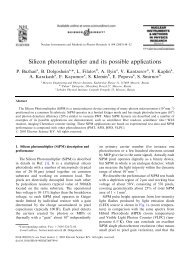
Figure 1. Overview <strong>of</strong> <strong>the</strong> VATA<strong>64</strong>-HDR16 <strong>ASIC</strong>.<br />
a better efficiency to identify <strong>the</strong> Cherenkov pattern.<br />
In this paper, we briefly describe <strong>the</strong> main functionalities<br />
<strong>of</strong> <strong>the</strong> new <strong>ASIC</strong> <strong>and</strong> a few preliminary<br />
results obtained with our first prototype test<br />
board.<br />
2. VATA<strong>64</strong>-HDR16: a <strong>front</strong>-<strong>end</strong> <strong>ASIC</strong> <strong>for</strong><br />
<strong>SiPM</strong> <strong>readout</strong><br />
The VATA<strong>64</strong>-HDR16 is a <strong>64</strong> channel <strong>front</strong>-<strong>end</strong><br />
<strong>ASIC</strong> based on <strong>the</strong> VATA architecture (<strong>for</strong> a short<br />
review on <strong>the</strong> early history <strong>of</strong> <strong>ASIC</strong>s <strong>for</strong> High Energy<br />
Physics see <strong>for</strong> instance [11]) <strong>and</strong> tailored<br />
<strong>for</strong> <strong>SiPM</strong> read-out. It has been specified in collaboration<br />
with GM-IDEAS [12] that developed<br />
<strong>the</strong> <strong>ASIC</strong> under a 0.35μm CMOS manufacturing<br />
process with an epitaxial protection against SEE<br />
effects in space applications. An overview <strong>of</strong> <strong>the</strong><br />
<strong>ASIC</strong> can be found in Fig. 1.<br />
All <strong>the</strong> <strong>ASIC</strong> main operational parameters can<br />
be programmed by downloading a “slow control”<br />
configuration after power-up.<br />
The analog signal processing takes place in<br />
<strong>the</strong> <strong>front</strong>-<strong>end</strong> channels <strong>of</strong> <strong>the</strong> device, while <strong>the</strong><br />
read-out is h<strong>and</strong>led in <strong>the</strong> back-<strong>end</strong>. Each channel<br />
consists <strong>of</strong> a charge sensitive preamplifier, a<br />
fast shaper <strong>for</strong> triggering <strong>and</strong> <strong>timing</strong> <strong>and</strong> a slow<br />
shaper to provide a charge measurement. The<br />
output <strong>of</strong> <strong>the</strong> fast shaper is fed into a discriminator.<br />
The architecture <strong>of</strong> <strong>the</strong> channel <strong>readout</strong> is<br />
shown in Fig. 2.<br />
At power-on, a threshold can be set <strong>and</strong> individually<br />
adjusted <strong>for</strong> each cannel.<br />
In auto-trigger mode, whenever a channel exceeds<br />
its threshold value, <strong>the</strong> (auto-)trigger signal is asserted.<br />
The trigger can be output to <strong>the</strong> global<br />
<strong>of</strong>f-chip trigger line <strong>and</strong> may also be used to generate<br />
an on-chip Sample-<strong>and</strong>-Hold (SH) signal.<br />
A Time-To-Analogue-Converter (TAC) is implemented<br />
as a voltage ramp initiated by <strong>the</strong> trigger
346<br />
M.G. Bagliesi et al. / Nuclear Physics B (Proc. Suppl.) 215 (2011) 344–348<br />
Figure 2. Architecture <strong>of</strong> one <strong>front</strong>-<strong>end</strong> channel <strong>of</strong> <strong>the</strong> VATA<strong>64</strong>-HDR16 <strong>ASIC</strong>.<br />
<strong>and</strong> sampled with <strong>the</strong> SH signal. The slow shaper<br />
is followed by a Peak & Hold device.<br />
The outputs <strong>of</strong> all channels are <strong>readout</strong> via two<br />
multiplexers running in parallel, one <strong>for</strong> <strong>the</strong> sampled<br />
slow shaper charge measurement <strong>and</strong> one <strong>for</strong><br />
<strong>the</strong> TAC values. The output <strong>of</strong> both multiplexers<br />
is made available via differential output current<br />
buffers. The <strong>ASIC</strong> can be sampled in three different<br />
ways:<br />
characterized by a number <strong>of</strong> hits detected simultaneously.<br />
3. The VATA<strong>64</strong>-HDR16 test board<br />
We developed a dedicated test-board, <strong>the</strong> VAB-<br />
HDR16 (see Fig. 3), equipped with all <strong>the</strong> circuitry<br />
<strong>for</strong> signal conditioning, digitization <strong>and</strong><br />
<strong>readout</strong>. For <strong>the</strong> <strong>readout</strong> <strong>of</strong> <strong>the</strong> current output<br />
• external sampling: this is <strong>the</strong> traditional<br />
VA sampling method;<br />
• internally generated sampling based on an<br />
internal trigger: a SH signal is issued at a<br />
programmable time delay;<br />
• internally generated sampling based on an<br />
external trigger: <strong>the</strong> <strong>ASIC</strong> senses <strong>the</strong><br />
TA/TB lines to check if any o<strong>the</strong>r <strong>ASIC</strong><br />
has triggered. The SH signal is issued at<br />
a programmable time delay.<br />
With <strong>the</strong> <strong>ASIC</strong> in “self-triggering” mode, whenever<br />
a channel exceeds its threshold it starts a<br />
new time measurement that is stopped after a<br />
programmable delay by <strong>the</strong> SH signal. In this<br />
way, we can measure <strong>the</strong> time differences between<br />
<strong>the</strong> first triggering channel <strong>and</strong> <strong>the</strong> o<strong>the</strong>r channels<br />
that have been hit. This functionality allows to<br />
define an <strong>of</strong>fline ”time window” to select events<br />
Figure 3. The VATA-HDR16 test board.
M.G. Bagliesi et al. / Nuclear Physics B (Proc. Suppl.) 215 (2011) 344–348 347<br />
buffers <strong>of</strong> <strong>the</strong> <strong>ASIC</strong>, two stages are used: <strong>the</strong> first<br />
one is a voltage feedback amplifier <strong>for</strong> current-tovoltage<br />
conversion, while <strong>the</strong> second one consists<br />
<strong>of</strong> a fully differential input <strong>and</strong> differential output<br />
device.<br />
For <strong>the</strong> analog to digital conversion, we used a 16<br />
bits, 1 MSPS, fully differential ADC. All configuration,<br />
control <strong>and</strong> <strong>readout</strong> signals were generated<br />
by an Altera FPGA <strong>of</strong> <strong>the</strong> Cyclone II family:<br />
<strong>the</strong> EP2C8T144. Our test-board is equipped<br />
with an USB 2 interface with a PC to download<br />
<strong>the</strong> configuration bits <strong>of</strong> <strong>the</strong> VATA<strong>64</strong>-HDR16, to<br />
read/write registers <strong>and</strong> to <strong>readout</strong> <strong>the</strong> digitized<br />
data.<br />
4. Tests <strong>of</strong> <strong>the</strong> VATA<strong>64</strong>-HDR16 with <strong>the</strong><br />
VAB-HDR16<br />
We report here on <strong>the</strong> preliminary tests per<strong>for</strong>med<br />
in our lab to verify <strong>the</strong> functionality <strong>of</strong><br />
<strong>the</strong> board <strong>and</strong> <strong>the</strong> <strong>ASIC</strong>. All <strong>the</strong> measurements<br />
reported below – relative to <strong>the</strong> pulse height linearity<br />
<strong>and</strong> <strong>the</strong> time response <strong>of</strong> <strong>the</strong> <strong>ASIC</strong> – were<br />
per<strong>for</strong>med with no <strong>SiPM</strong> devices connected to<br />
<strong>the</strong> test board.<br />
Pulse height linearity tests were per<strong>for</strong>med injecting<br />
known values <strong>of</strong> charge into <strong>the</strong> <strong>ASIC</strong> input.<br />
The VATA<strong>64</strong>-HDR16 showed a linear response<br />
<strong>for</strong> charges up to 12 pC (Fig. 4). For<br />
larger charges, a saturation effect was observed.<br />
The pedestal rms width could be lowered to σ ∼<br />
1 fC with simple EMI reduction precautions by<br />
shielding <strong>the</strong> board.<br />
The result <strong>of</strong> a test on <strong>the</strong> linearity <strong>of</strong> <strong>the</strong> time<br />
measurement is reported in Fig. 5. The first triggering<br />
channel was set to produce a constant time<br />
output t max whose value was set via <strong>the</strong> programmable<br />
SH time delay. We injected charge in<br />
a second channel at various delays with respect to<br />
<strong>the</strong> first one: <strong>the</strong> generated time-stamp showed a<br />
good linearity up to several hundreds <strong>of</strong> nanoseconds.<br />
The width <strong>of</strong> <strong>the</strong> time pedestal was found to be<br />
around σ ∼ 4 ADC units, i.e. 160 ps. (Fig. 6).<br />
Figure 4. Measurement <strong>of</strong> <strong>the</strong> pulse height linearity<br />
<strong>of</strong> <strong>the</strong> <strong>ASIC</strong>.<br />
5. Conclusions<br />
The basic functionalities <strong>of</strong> a new <strong>ASIC</strong>, specifically<br />
designed <strong>for</strong> <strong>SiPM</strong> <strong>readout</strong>, were tested using<br />
a <strong>custom</strong> test board. In a following paper<br />
we will report on our measurements – both in<br />
<strong>the</strong> lab <strong>and</strong> at a dedicated beam test – with<br />
<strong>SiPM</strong> photodetectors connected to <strong>the</strong> <strong>ASIC</strong>. At<br />
present, we are integrating <strong>the</strong> new <strong>ASIC</strong> <strong>readout</strong><br />
into <strong>SiPM</strong>-based prototypes <strong>of</strong> RICH <strong>and</strong> DIRC<br />
Cherenkov detectors.<br />
Acknowledgments<br />
The authors would like to thank Altera Inc. <strong>for</strong><br />
supporting <strong>the</strong> project through <strong>the</strong> Altera University<br />
program. This work has been funded by<br />
<strong>the</strong> Istituto Nazionale di Fisica Nucleare (INFN)<br />
in Italy in cooperation with GM-Ideas.<br />
REFERENCES<br />
1. V. Saveliev, V. Golovin et al., Nucl. Instrum.<br />
Meth. A 442 (2000) 223
348<br />
M.G. Bagliesi et al. / Nuclear Physics B (Proc. Suppl.) 215 (2011) 344–348<br />
Figure 5. Measurement <strong>of</strong> <strong>the</strong> time linearity <strong>of</strong><br />
<strong>the</strong> <strong>ASIC</strong>. The anti-correlation shown in <strong>the</strong> figure<br />
is due to <strong>the</strong> <strong>of</strong>fset in <strong>the</strong> time-stamp <strong>of</strong> <strong>the</strong><br />
first trigger which occurs at t max<br />
2. P. Buzhan, B. Dolgoshein et al., Nucl. Instrum.<br />
Meth. A 504 (2003) 48-52<br />
3. V. Golovin et al., Nucl. Instrum. Meth. A 518<br />
(2004) 560-5<strong>64</strong><br />
4. N. Dinu et. al., Nucl. Instrum. Meth. A 572<br />
(2007) 422-426<br />
5. M. Danilov, Nucl. Instrum. Meth. A 604<br />
(2009) 183-189<br />
6. T. Frach, G. Prescher <strong>and</strong> C. Degenhardt,<br />
Silicon photomultiplier technology goes fullydigital,<br />
January 2010 Electronic Engineering<br />
Times Europe, (2010) 10-11<br />
7. C. Piemonte, et al., Recent developments on<br />
silicon photomultipliers produced at FBKirst,<br />
in: IEEE NSS MIC 2007 Conference<br />
Record, N41-2, (2007) 20892092<br />
8. G. Llosa et al., First PET Imaging Results<br />
with Continuous LYSO Crystals <strong>and</strong> Monolithic,<br />
<strong>64</strong>-Pixel <strong>SiPM</strong> Matrices, in: IEEE NSS<br />
MIC 2010 Conference Record, M19-70<br />
9. Hamamatsu Photonics K.K., documentation<br />
<strong>of</strong> <strong>the</strong> multi-pixel photon counter, available at<br />
http://jp.hamamatsu.com/<br />
Figure 6. A typical time pedestal <strong>of</strong> one channel<br />
<strong>of</strong> <strong>the</strong> board during charge injection tests.<br />
10. http://sensl.com/products/siliconphotomultipliers/spmmatrix/<br />
11. G. Hall, Recent progress in <strong>front</strong> <strong>end</strong> <strong>ASIC</strong>s<br />
<strong>for</strong> high-energy physics, Nucl. Instr. Meth. A<br />
541 (2005) 248-258<br />
12. IDEAS ASA, Norway, VATA<strong>64</strong>-HDR16 documentation