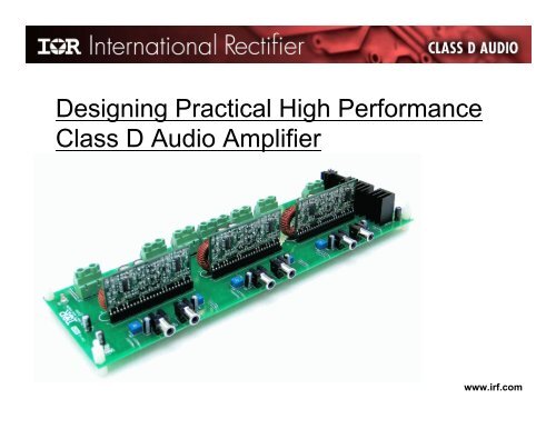
Designing Practical High Performance Class D Audio Amplifier
Designing Practical High Performance Class D Audio Amplifier
Designing Practical High Performance Class D Audio Amplifier
Create successful ePaper yourself
Turn your PDF publications into a flip-book with our unique Google optimized e-Paper software.
<strong>Designing</strong> <strong>Practical</strong> <strong>High</strong> <strong>Performance</strong><br />
<strong>Class</strong> D <strong>Audio</strong> <strong>Amplifier</strong><br />
www.irf.com
Contents<br />
Chapter 1<br />
Chapter 2<br />
Chapter 3<br />
Chapter 4<br />
• <strong>Class</strong> D <strong>Amplifier</strong> Introduction<br />
Theory of class D operation, Points of design<br />
• The latest Digital <strong>Audio</strong> MOSFET,<br />
DirectFET ® MOSFET<br />
Importance of layout and packaging<br />
Optimized MOSFET for no-heat sinking<br />
• <strong>Designing</strong> Dead-time and Overload<br />
Protection with Digital <strong>Audio</strong> Gate<br />
Driver IC<br />
<strong>Designing</strong> with built-in dead-time generation<br />
How to design OCP. Tj estimation.<br />
• Design Example<br />
No-heat sink 100W x 6ch compact <strong>Class</strong> D amplifier<br />
www.irf.com
Chapter 1 <strong>Class</strong> D <strong>Audio</strong> Overview<br />
www.irf.com
Review: Traditional <strong>Class</strong> AB <strong>Amplifier</strong><br />
Feed back<br />
+Vcc<br />
• <strong>Class</strong> AB amplifier uses<br />
linear regulating transistors<br />
to modulate output voltage.<br />
+<br />
-<br />
Error amp<br />
+<br />
Bias<br />
-Vcc<br />
η = 30% at temp rise test condition.<br />
• A loss in the regulating<br />
transistor in <strong>Class</strong> AB<br />
amplifier is proportional to<br />
the product of the voltage<br />
across the device and the<br />
current flowing through it.<br />
P<br />
C<br />
= V<br />
CE<br />
⋅ I<br />
C<br />
Independent of device<br />
parameter<br />
www.irf.com
<strong>Class</strong> D <strong>Amplifier</strong><br />
Feed back<br />
Triangle<br />
+VCC<br />
Nch<br />
Level Shift<br />
+<br />
-<br />
Error Amp<br />
COMP<br />
Dead Time<br />
Nch<br />
+<br />
-VCC<br />
•<strong>Class</strong> D amplifier employs MOSFETs which are either<br />
ON or OFF state. Therefore ideally 100% efficiency can<br />
be achieved.<br />
•PWM technique is used to express analog audio signals<br />
with ON or OFF states in output devices.<br />
•A loss in the switching device caused by 1)finite<br />
transition speed, 2)ON state resistance and 3)gate<br />
charge.<br />
P TOTAL<br />
= Psw + Pcond + Pgd<br />
dependent of device parameter can be improved further!<br />
www.irf.com
Basic PWM Operation<br />
The output signal of comparator<br />
goes high when the sine wave is<br />
higher than the sawtooth.<br />
COMP<br />
<strong>Class</strong> D<br />
switching stage<br />
LPF<br />
Using f PWM<br />
=400kHz to modulate 25kHz sinusoidal waveform<br />
www.irf.com
Major Causes of Imperfection<br />
Pulse width error<br />
Quantization error<br />
Perturbation<br />
Zo<br />
Bus Pumping<br />
+VCC<br />
Nonlinear inductance /<br />
Capacitance<br />
DC Resistance<br />
<strong>Audio</strong> source<br />
PWM<br />
Gate Driver<br />
An ideal <strong>Class</strong> D amplifying<br />
stage has no distortion and no<br />
noise generation in the audible<br />
band, along with providing<br />
100% efficiency. However, as<br />
shown, practical <strong>Class</strong> D<br />
amplifiers have imperfections<br />
that generate distortions and<br />
noise.<br />
Dead time<br />
Delay time<br />
ON delay<br />
Finite dV/dt<br />
RDS(ON)<br />
-VCC<br />
OFF delay<br />
Finite Rds(on)<br />
Vth and Qg<br />
Body diode recovery<br />
Stray inductances<br />
0.01% of non-linearity<br />
corresponds to<br />
10mV out of 100V DC bus<br />
or 0.25ns out of 400kHz.<br />
www.irf.com
Three Difficulties in <strong>Class</strong> D Design<br />
• PCB Layout<br />
• Dead-time Generation<br />
• Overload Protection<br />
Direct-FET, Half-bridge MOSFET<br />
can eliminate influences from stray<br />
inductances.<br />
Integrated Gate Driver IC<br />
can make things easier<br />
www.irf.com
Chapter 2 DIGITAL AUDIO MOSFET<br />
The right power switch for <strong>Class</strong>-D audio amplifiers<br />
www.irf.com
Digital <strong>Audio</strong> MOSFET introduction<br />
• Digital <strong>Audio</strong> MOSFET is specifically designed for<br />
<strong>Class</strong>-D audio amplifier applications<br />
• Key parameters such as R DS(on) , Q g , and Q rr are<br />
optimised for maximizing efficiency, THD and EMI<br />
amplifier performance<br />
• Low internal R G distribution guaranteed for better<br />
dead time control<br />
• New and innovative packages offer greater<br />
flexibility and performance<br />
• These features make IR Digital <strong>Audio</strong> MOSFETs the<br />
right power switches for <strong>Class</strong>-D audio amplifiers!!<br />
www.irf.com
IRF6665 DirectFET ®<br />
The best MOSFET for Mid-Power<br />
<strong>Class</strong>-D amplifier applications<br />
www.irf.com
IRF6665 Digital <strong>Audio</strong> MOSFET<br />
• IRF6665 Digital <strong>Audio</strong> MOSFET combines the latest<br />
IR medium voltage trench silicon with the advanced<br />
DirectFET ® package<br />
• Key parameters, such as R DS(on) , Q g , Q sw , and Q rr are<br />
optimized for mid-power <strong>Class</strong>-D audio amplifier<br />
applications<br />
• IRF6665, has all the characteristics to be the best<br />
power switch for mid-power amplifiers!!<br />
www.irf.com
DirectFET ® device technology<br />
SO-8<br />
Multiple gold<br />
wirebonds<br />
DirectFET ®<br />
passivated die<br />
copper ‘drain’<br />
clip<br />
die attach<br />
material<br />
copper drain<br />
leads<br />
copper<br />
source leads<br />
• Drain/source leads and<br />
wirebonds contribute to both<br />
package resistance and<br />
inductance<br />
• Majority of heat transferred<br />
through leads to PCB board<br />
gate<br />
connection<br />
copper track<br />
on board<br />
source<br />
connection<br />
• Remove wirebonds from package<br />
and replace with large area solder<br />
contacts<br />
• Reduced package inductance and<br />
resistance<br />
• Copper can enables dual sided<br />
cooling<br />
www.irf.com
DirectFET ® : low inductance package for audio<br />
• Lower inductance at frequency than SO-8, D-Pak, MLP and D-Pak<br />
• TO-220 inductance package is ~ 12nH<br />
www.irf.com
Advantages of DirectFET ® : Reduce ringing<br />
• Inductance related ringing reduced compared to SO-8<br />
• Example below for DirectFET ® and SO-8 switching 30A at 500kHz<br />
• Silicon of the near identical active area, voltage and generation<br />
used in both packages<br />
DirectFET ® waveform<br />
SO-8 waveform<br />
www.irf.com
IRF6665 for class-D audio applications<br />
Key Parameters<br />
Parameter Min Typ Max Units<br />
V(BR)DSS 100 - - V<br />
RDS(ON) @ VGS = 10V - 53 62 mOhms<br />
Qg - 8.4 13.0 nC<br />
Qgd - 2.8 - nC<br />
Qsw - 3.4 - nC<br />
RG (int) - 1.9 2.9 Ohms<br />
VGS(TH) 3 - 5 V<br />
• Refer to IRF6665 datasheet for further details<br />
www.irf.com
IRF6665 DirectFET ® Evaluation Board<br />
Spec:<br />
Power Supply ±35.0V<br />
Output Power 150W+150W, 4Ω<br />
MOSFET IRF6665<br />
Gate Driver IR2011S<br />
DirectFET® IRF6665<br />
IR2011S<br />
www.irf.com
Efficiency Data<br />
Test Conditions: Half-Bridge Configuration, Vbus = +/- 35V, fswitching = 395kHz,<br />
finput = 1kHz, Rload = 4 and 8 Ohms<br />
Rload = 8Ω<br />
Rload = 4Ω<br />
Rload (Ω)<br />
4<br />
8<br />
Efficiency @ 1%THD<br />
94.8<br />
96.0<br />
www.irf.com
THD+N Data<br />
Test Conditions: Half-Bridge Configuration, Vbus = +/- 35V, fswitching = 395KHz,<br />
finput = 1KHz, Rload = 4 and 8 Ohms<br />
Rload (Ω)<br />
4<br />
8<br />
THD + N @ 1/8 Pout<br />
0.0057<br />
0.0031<br />
Rload = 8Ω<br />
Rload = 4Ω<br />
www.irf.com
VDS Switching Waveforms<br />
• DirectFET ® package shows cleanest and fastest (approx. three times faster)<br />
switching waveforms than amplifier with TO-220 package.<br />
• Same IRF6665 MOSFET die is tested in both packages<br />
DirectFET ®<br />
Package<br />
Blue : V GS<br />
Pink : V DS<br />
TO-220<br />
package<br />
www.irf.com
EMI Data @ 1/8 Pout Condition (12.5W)<br />
• DirectFET ® and TO-220 with the same IRF6665 silicon die<br />
• MosFET devices with no heatsink<br />
• No shielded room<br />
• Over 2MHz, DirectFET ® amplifier shows approximately 9dB lower noise<br />
than TO-220 amplifier<br />
• Under 2MHz, background noise is dominant<br />
Frequency (MHz)<br />
DirectFET ®<br />
Frequency (MHz)<br />
TO-220<br />
CISPR13<br />
Quasi-Peak Limits<br />
Average Limits<br />
CISPR13<br />
Quasi-Peak Limits<br />
Average Limits<br />
www.irf.com
Typical Case Scenario<br />
Thermal <strong>Performance</strong><br />
No Heatsink<br />
Worst Case Scenario<br />
Test Conditions:<br />
100W/8Ω, 1% THD, +/- 45Vbus,<br />
fsw=400KHz, T AMBIENT<br />
~ 25°C<br />
Case Temperature (°C)<br />
120<br />
100<br />
80<br />
60<br />
40<br />
20<br />
<strong>Amplifier</strong> specs: 100W/8Ω<br />
full power<br />
Estimated Plosses=1.6W<br />
1/8 power<br />
Estimated Plosses=0.6W<br />
After 10 minutes IRF6665 case<br />
temperature = 80.1°C @ 100W/8Ω<br />
without heatsink (ΔTc = 55.1°C)<br />
0<br />
T AMBIENT<br />
~ 20 °C<br />
0 100 200 300 400 500<br />
Time (s)<br />
Full Power: T C =104°C @ 5min (ΔT C =83°C)<br />
1/8 Power: T C =58°C @ 5min (ΔT C =39°C)<br />
www.irf.com
Assembling IRF6665 in audio <strong>Class</strong>-D circuits<br />
• Stencil on solder paste<br />
• Pick and place devices onto pads<br />
• Re-flow devices<br />
If additional heatsink is needed for higher power,<br />
• Place thermal interface material over devices<br />
• Place heatsink over device/thermal interface stack<br />
• Secure heatsink in place with screws<br />
• PCM burned in to wet out interface between can and heatsink<br />
• Screw torques reset when assembly has cooled<br />
www.irf.com
Thermal <strong>Performance</strong><br />
with Heatsink<br />
• Individual DirectFET ® MOSFET audio reference boards<br />
assembled with 3 different phase change materials<br />
• Heatsink applied to assembly<br />
– Fischer SK04, 3.8”X0.6”, 0.6” extrusion, black anodised, 3°CW -1<br />
• Constant power applied to device junctions to simulate<br />
100W amplifier operation:<br />
– Normal operation conditions (1/8 full output power) into 4Ω and 8Ω<br />
– Full output power into 4Ω and 8Ω<br />
• Case temperature was monitored before and during<br />
application of power to the junctions with<br />
thermocouples applied between can and heatsink<br />
www.irf.com
Temperature difference (°C)<br />
100<br />
90<br />
80<br />
70<br />
60<br />
50<br />
40<br />
30<br />
20<br />
10<br />
0<br />
ΔT CASE versus time<br />
No significant difference between<br />
the PCM materials used<br />
0 100 200 300 400 500<br />
Time (s)<br />
100W into 4Ω<br />
Power/device* = 2.4W<br />
100W into 8Ω<br />
Power/device* = 1.6W<br />
12.5W into 4Ω & 8Ω<br />
(1/8 of 100W)<br />
Power/device* = 0.6W<br />
<strong>Amplifier</strong> Conditions<br />
12.5W (1/8) into 4 & 8Ω<br />
100W into 8Ω<br />
100W into 4Ω<br />
Plosses* Temperature rise (°C) after 5 min<br />
per<br />
device Material<br />
-<br />
A Material<br />
-<br />
B Material<br />
-<br />
C<br />
0.6 22.1<br />
24.8<br />
23.4<br />
1.6<br />
2.4<br />
(*) Estimated Plosses @ worst case scenario<br />
52.7<br />
77.1<br />
58.2<br />
82.8<br />
55.1<br />
76.4<br />
www.irf.com
Half-Bridge Full-Pak<br />
Another Innovative Package for <strong>Class</strong> D <strong>Audio</strong><br />
<strong>Amplifier</strong> Application<br />
www.irf.com
Half-Bridge Full-Pak<br />
⇒<br />
S2<br />
G2<br />
D2/S1<br />
G1<br />
D1<br />
TO-220 Full-Pak<br />
5 PIN<br />
• 55V, 100V, 150V and 200V devices to be released on Q3 ‘06<br />
• 55V: IRFI4024H-117<br />
• 100V: IRFI4212H-117<br />
• 150V: IRFI4019H-117<br />
• 200V: IRFI4020H-117<br />
www.irf.com
Half-Bridge Full-Pak Features<br />
• Integrated Half-Bridge Package<br />
• Reduces the part count by half<br />
• Reduced package inductance improves EMI performance<br />
• Facilitates better PCB layout<br />
• Enables single layer PCB layout in combination with<br />
IR2011S<br />
• Low R G(int)<br />
distribution for better dead time control<br />
• Lead-Free package<br />
Reduce devices number,<br />
stray inductance and<br />
facilitates layout and<br />
assembly<br />
IRFI4024H-117 www.irf.com + IR2011S
Disturbance Power<br />
Half-Bridge Full-Pak vs. TO-220 (single die)<br />
• Half-Bridge Full-Pak amplifier shows better performance than TO-220 amplifier.<br />
Approximately 10dB lower disturbance power level.<br />
180VAC @ 50Hz, Speaker Output<br />
Half-Bridge Full-Pak<br />
TO-220<br />
Same MOSFET silicon die in both<br />
packages<br />
www.irf.com
Summary<br />
• DirectFET ® devices are ideal candidates for use in <strong>Class</strong>-<br />
D audio amplifier applications<br />
• Evaluations of IRF6665 in <strong>Class</strong>-D audio amplifier<br />
demonstrated improved efficiency, THD, and EMI<br />
• Utilising DirectFET ® technology reduces EMI compared<br />
to TO-220 packages<br />
• Thermal evaluations demonstrated that IRF6665 can<br />
deliver up to 100W per channel into 8Ω with no heatsink<br />
• Half-Bridge Full-Pak features make this device an<br />
excellent option for <strong>Class</strong>-D audio amplifier applications<br />
— Integrated half-bridge package reduces the part count by half<br />
— Low package inductance improves EMI performance<br />
• Digital <strong>Audio</strong> MOSFET is the right switch for <strong>Class</strong>-D<br />
audio amplifiers!!<br />
www.irf.com
Conclusion 1<br />
• With IR’s DirectFET ® technology, <strong>Class</strong> D<br />
amplifier reaches the point where 100W amplifier<br />
can be built without heat sink<br />
• Optimum package provides the best audio<br />
performance along with minimum EMI emissions<br />
• Optimum silicon design provides the best<br />
efficiency over 95%<br />
www.irf.com
Chapter 3 DIGITAL AUDIO Gate Driver<br />
www.irf.com
Protected DIGITAL AUDIO Gate Driver IC<br />
IRS20124<br />
•Programmable Discrete Deadtime<br />
(PAT.Pending)<br />
•Programmable Bi-directional<br />
Over Current Sensing<br />
(PAT.Pending)<br />
•200V high voltage ratings to deliver up to<br />
1000W output power in <strong>Class</strong> D audio<br />
amplifier applications<br />
•Simplifies design due to integrated deadtime<br />
generation and bi-directional over<br />
current sensing<br />
•Optimized and compensated preset deadtime<br />
selections for improved THD<br />
performances over temperature and noise<br />
•Shutdown function to protect devices from<br />
overloaded conditions<br />
•Operates up to 1MHz<br />
•3.3V/5V logic compatible input<br />
V SUPPLY<br />
200V max<br />
I O<br />
+/-1.0A / 1.2A<br />
Selectable Dead-time 15/25/35/45nS<br />
Prop Delay time 70ns<br />
14pin SOIC<br />
www.irf.com
OCSET1<br />
OCSET2<br />
<strong>High</strong><br />
Voltage<br />
Level<br />
Shifter<br />
UVLO<br />
UV<br />
S<br />
R<br />
Q<br />
VB<br />
HO<br />
OC<br />
Current<br />
Sensing<br />
<strong>High</strong> Side Floating Well<br />
VS<br />
DT/SD<br />
Comparator<br />
Vcc<br />
UVLO<br />
IN<br />
Dead-time<br />
Gen<br />
Shutdown<br />
Logic<br />
IRS20124<br />
Matching<br />
Delay<br />
LO<br />
COM<br />
www.irf.com
The discrete dead-time<br />
method sets a dead-time by<br />
selecting one of the preset<br />
values from outside of the<br />
IC. Comparing with previous<br />
program method, the<br />
discrete dead-time can<br />
provide a precise dead-time<br />
insertion, regardless of noise<br />
injection in DT pin. Thus, the<br />
dead-time setting value can<br />
be set tighter, which is highly<br />
beneficial for the THD<br />
performance in <strong>Class</strong> D<br />
applications.<br />
Discrete Dead-time<br />
Operation Mode<br />
15nS<br />
25nS<br />
35nS<br />
45nS<br />
>0.5mA<br />
R1<br />
R2<br />
IRS20124<br />
Vcc<br />
DT/SD<br />
COM<br />
Shutdown<br />
0.23xVcc<br />
0.36xVcc<br />
0.57xVcc<br />
0.89xVcc<br />
Vcc<br />
V DT<br />
Noise injection<br />
www.irf.com
IRS20124 THD+N <strong>Performance</strong><br />
V CC : ±35.0V<br />
Gate Driver: IRS20124<br />
MOSFET: IRFB4212<br />
f PWM = 400kHz<br />
Note that low THD+N<br />
characteristic shows<br />
quiet noise floor due to<br />
clean and stable<br />
switching timings.<br />
Dead-time Settings:<br />
DT1 = 15ns<br />
DT2 = 25ns<br />
DT3 = 35ns<br />
DT4 = 45ns<br />
www.irf.com
Overload Protection in <strong>Class</strong> AB<br />
B+<br />
Ov erload<br />
X1<br />
Equivalent circuit<br />
TIP3055<br />
Q1<br />
220m<br />
R1<br />
2.2k<br />
R3<br />
Q2N3904<br />
Q3<br />
220m<br />
R6<br />
Overload<br />
2.2k<br />
R7<br />
220m<br />
R2<br />
10k<br />
R4<br />
R LOAD<br />
1K<br />
R5<br />
Q2N3904<br />
Q4<br />
D2<br />
D1N4148<br />
TIP2955<br />
Q2<br />
D1<br />
D1N4148<br />
R LOAD<br />
8<br />
R8<br />
10k<br />
R9<br />
B-<br />
When a <strong>Class</strong> AB amplifier has a shorted load,<br />
the load current can ramp up rapidly. The voltage<br />
across the device is fixed to the bus voltage.<br />
The loss in the device is enormous amount<br />
The power devices can not be protected<br />
with over current detection method<br />
Therefore an impedance bridge has been<br />
commonly used, which has following drawback;<br />
• Reactive components in the load impedance,<br />
which is common in realistic loudspeakers,<br />
causes false protection<br />
www.irf.com
Overload Protection in <strong>Class</strong> D<br />
Over Current Detection<br />
Load<br />
When a <strong>Class</strong> D amplifier has a shorted load,<br />
there still is a LPF inductor in between the load<br />
and the amplifier. Therefore, the load current<br />
ramps up at a rate of Vo/L.<br />
The loss in the device is determined by the R DS(ON)<br />
and the load current.<br />
Over current detection works very good in<br />
<strong>Class</strong> D<br />
Benefits from over current detection;<br />
• Trip level is independent of phase shift in the<br />
load current<br />
• The amplifier can sustain any instantaneous<br />
low load impedance until the load current<br />
reaches the trip level<br />
www.irf.com
Why Bi-Directional CS?<br />
Load<br />
Load<br />
Load<br />
Inductor Current<br />
Load current flows through the low-side MOSFET<br />
unless the high duty cycle reaches 100%, where no<br />
conduction period exists in the low-side MOSFET.<br />
Since 100% duty cycle is not allowed due to highside<br />
bootstrap power supply operation, the amount<br />
of current sensed from the low side MOSFET covers<br />
full cycle of an audio signal.<br />
<strong>High</strong> Side ON<br />
Low Side ON<br />
www.irf.com
Benefits of Bi-Directional CS<br />
More than just cost savings…<br />
Bi-directional current sensing<br />
provides following technical<br />
benefits.<br />
Conventional Current Sensing<br />
100n<br />
C2<br />
IRF530<br />
Q1<br />
22u<br />
Q4<br />
L1<br />
50<br />
V2<br />
•Minimum stray inductance in power stage<br />
current path due to no additional current<br />
sensing components in the path<br />
5<br />
V1<br />
W=1u<br />
L=1u<br />
Q3<br />
W=1u<br />
L=1u<br />
IRF530<br />
Q2<br />
470n<br />
C1<br />
20m<br />
R1<br />
L2<br />
50n<br />
Shunt Resistor<br />
8<br />
R2<br />
50<br />
V3<br />
•No influences in measured current from gate<br />
charge current and reverse recovery charge<br />
current<br />
•Positive Temp/Co in R DS(ON) reduces the trip<br />
level at high junction temperature in real time<br />
Shunt<br />
Resistors<br />
With IRS20124<br />
•Adding a shunt resistor causes<br />
ringing by adding stray inductances.<br />
•The current includes gate<br />
charge/discharge current and<br />
reverse recovery charge current.<br />
•Imbalance of effective R DS(ON) in<br />
high and low sides causes distortion.<br />
100n<br />
C3<br />
www.irf.com
What happens in the Short Circuit Event?<br />
Vo<br />
Zo<br />
5<br />
V1<br />
100m<br />
R1<br />
<strong>Class</strong> D<br />
amplifier<br />
L<br />
18u<br />
L1<br />
C<br />
0.47u<br />
C1<br />
R L<br />
8<br />
R2<br />
Short<br />
V<br />
Z<br />
O<br />
O<br />
di<br />
dt<br />
=<br />
V<br />
L<br />
O<br />
Without<br />
Shutdown<br />
5<br />
V1<br />
100m<br />
R1<br />
18u<br />
L1<br />
0<br />
I TRIP<br />
Now the <strong>Class</strong> D amplifier is driving an inductor in<br />
the LPF. Note that the audio frequency<br />
components induce quite large volt-second<br />
feeding into the inductor, causing excessive<br />
inductor current in the event of short circuit load.<br />
When short circuit occurs, the load current starts to<br />
ramp up quickly with a gradual rate of Vo/L. Since an<br />
inductor is in between the amplifier and the load,<br />
short current may not exceed the trip level.<br />
I L<br />
I L<br />
Shutdown<br />
Short Circuit<br />
With<br />
Shutdown<br />
Inductor<br />
discharge<br />
A junction temperature at the end of the protection<br />
event can be estimated by using a thermal transient<br />
model in IR’s Digital <strong>Audio</strong> MOSFET to ensure the<br />
functionality.<br />
After the shutdown, the energy stored in the inductor<br />
discharges to the power supply, only the waveform<br />
of the current contributes the loss in the MOSFET.<br />
www.irf.com
How to Design with OC Function<br />
IRS20124<br />
IRS20124<br />
PWM input<br />
Gate Driver<br />
PWM input<br />
Gate Driver<br />
SD<br />
SD<br />
O<br />
C<br />
Vs Sensing<br />
Ext. Latch<br />
OC<br />
Vs Sensing<br />
With the OC pin connected to DT/SD pin, the output<br />
signal out of OC at the event of over current will be<br />
removed by its output itself when the IRS20124 goes<br />
into shutdown mode. This could cause a hiccup in the<br />
protection sequence.<br />
One simple way to assure shutdown upon an over<br />
current detection is to attach a latch circuitry onto the<br />
OC pin, as shown.<br />
www.irf.com
In Negative Half Cycle<br />
IRS20124 OC Functionality<br />
OC pin<br />
In Positive Half Cycle<br />
1kHz, 20W<br />
Inductor<br />
discharge<br />
Switching node<br />
Inductor current<br />
The bi-directional current sensing can capture<br />
over current conditions at either positive or<br />
negative current direction. In this<br />
demonstration, the threshold for Vs is set to be<br />
±1V by setting OC SET1<br />
=1V and OC SET2<br />
=3V,<br />
which can be translated into 15A trip level with<br />
70mΩ R DS(ON)<br />
.<br />
Short circuit occurred<br />
Shutdown by OC<br />
www.irf.com
IRS20124 OC Functionality - Vs Waveform<br />
Vs<br />
Load<br />
These are close up shots of overload protection with magnified waveform of Vs. At the instance<br />
voltage at Vs reaches trip level, which is ±1V in this setting, OC pin shuts down the switching and<br />
the MOSFET is protected.<br />
Red: Vs node, 1V/div<br />
Green: OC pin w/10kΩ pull-up, 5V/div<br />
10µS/div<br />
Red: Vs node, 1V/div<br />
Green: OC pin w/10kΩ pull-up, 5V/div<br />
10µS/div<br />
www.irf.com
Tj Estimation in Short Circuit Event<br />
All the DIGITAL AUDIO MOSFET have thermal<br />
equivalent circuit on the datasheet for transient<br />
thermal analysis. The junction temperature of the<br />
MOSFET at the end of the over current protection<br />
event can be estimated using this model along with<br />
the waveform from the bench evaluations.<br />
Transient Thermal Impedance<br />
(Excerpt from IRF6665 Datasheet)<br />
current<br />
Duty<br />
V3<br />
0.85<br />
V1<br />
V(n1)*V(n2)<br />
ARB2<br />
N1 OUT<br />
N2<br />
Shutdown<br />
Vs<br />
LO<br />
Duty<br />
dI/dt<br />
Peak current<br />
0.051<br />
V2<br />
Tj<br />
V(n1)*(V(n2)*0.007692+0.808)<br />
ARB1<br />
N1 OUT<br />
N2<br />
Pd<br />
Rds<br />
Rds<br />
N2<br />
N1<br />
V(n1)*V(n2)<br />
ARB3<br />
N1 OUT<br />
N2<br />
Vds<br />
ARB4<br />
(-1)*V(n1)*V(n1)*V(n2)<br />
Id(ave)<br />
I L<br />
Tj<br />
667.6m<br />
R1<br />
1.0462<br />
R2<br />
1.56111<br />
R3<br />
29.2822<br />
R6<br />
25.455<br />
R7<br />
Duration<br />
98.9u IC=25<br />
C1<br />
0.856m IC=25<br />
C2<br />
2.81m IC=25<br />
C3<br />
23.4m IC=25 1.257 IC=25<br />
C5<br />
C6<br />
Commuted to the<br />
other side<br />
An Example of Tj Simulation using a Circuit Simulator<br />
www.irf.com
Tj Estimation Simulation Result<br />
3<br />
2.5<br />
T J =50ºC<br />
2<br />
1.5<br />
V DS<br />
V<br />
45<br />
40<br />
35<br />
30<br />
25<br />
20<br />
15<br />
10<br />
I D =43A<br />
Tj<br />
I D<br />
V<br />
1<br />
0.5<br />
0<br />
-0.5<br />
0 20 40 60 80 100<br />
Time/µSecs<br />
64<br />
62<br />
64mΩ<br />
20µSecs/div<br />
60<br />
5<br />
58<br />
0<br />
Time/µSecs<br />
10 20 30 40 50 60 70 80 90<br />
100uS<br />
10µSecs/div<br />
mV<br />
56<br />
54<br />
R DS(ON)<br />
52<br />
50<br />
48<br />
51mΩ<br />
0 20 40 60 80 100<br />
Time/µSecs<br />
20µSecs/div<br />
www.irf.com
Chapter 4 Design Example<br />
www.irf.com
100W x 6 Channels Design<br />
Specs:<br />
Supply Voltage: ±35V<br />
Output Power: 6ch x 100W into 8 ohm<br />
Protections: OCP, DC, OTP, OVP<br />
IR devices: IRS20124, IRF6665<br />
Dimensions: 295mm x 95mm x 40mm(H)<br />
CH-1 CH-2 CH-3 CH-4 CH-5 CH-6<br />
PROTECTION<br />
100W+100W MODULE 100W+100W MODULE 100W+100W MODULE<br />
POWER SUPPLY<br />
Single layer board<br />
www.irf.com
Design: 100W+100W Module<br />
• IR’s latest technology allows<br />
continuous 100W+100W audio<br />
outputs with no heat sink attached.<br />
• All the critical current paths are<br />
included in the module so that a single<br />
layer PC board can be used.<br />
• All the tricky functions, such as deadtime<br />
generation and over current<br />
protection, are included inside the<br />
module.<br />
• Over temperature protection<br />
• Digital <strong>Audio</strong> Direct-FET IRF6665 and<br />
Digital <strong>Audio</strong> gate driver IRS20124<br />
placed back to back are a perfect<br />
combination to obtain minimal stray<br />
inductances.<br />
30mm<br />
IRS20124<br />
65mm<br />
IRF6665<br />
Direct-FET<br />
www.irf.com
Design Test Results<br />
THD+N <strong>Performance</strong>, ±35.0V, 4 ohm load<br />
Switching Waveforms (10nS/div, 20V/div)<br />
120W @THD=1%<br />
170W @THD=10%<br />
f SW<br />
=430kHz<br />
THD=0.01%@50W<br />
Noise=62uVrms (IHF-A)<br />
S/N=110dB<br />
www.irf.com
Conclusion 2<br />
By using IR’s Digital <strong>Audio</strong> Gate Drivers and MOSFETs,<br />
• <strong>Class</strong> D audio amplifier design is no longer a<br />
do-it-by-feel trial and error process.<br />
• <strong>Class</strong> D amplifier is now entering a new age of<br />
do-it-yourself design with superior efficiency,<br />
performance and ruggedness.<br />
Visit IR’s <strong>Audio</strong> Website for more information:<br />
http://www.irf.com/product-info/audio/<br />
www.irf.com


