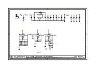
Optical receiver Board Appendix D
Optical receiver Board Appendix D
Optical receiver Board Appendix D

You also want an ePaper? Increase the reach of your titles
YUMPU automatically turns print PDFs into web optimized ePapers that Google loves.
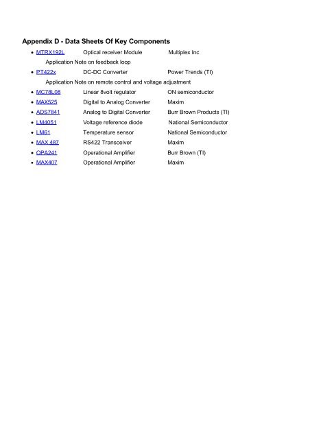
<strong>Appendix</strong> D - Data Sheets Of Key Components<br />
• MTRX192L <strong>Optical</strong> <strong>receiver</strong> Module Multiplex Inc<br />
Application Note on feedback loop<br />
• PT422x DC-DC Converter Power Trends (TI)<br />
Application Note on remote control and voltage adjustment<br />
• MC78L08 Linear 8volt regulator ON semiconductor<br />
• MAX525 Digital to Analog Converter Maxim<br />
• ADS7841 Analog to Digital Converter Burr Brown Products (TI)<br />
• LM4051 Voltage reference diode National Semiconductor<br />
• LM61 Temperature sensor National Semiconductor<br />
• MAX 487 RS422 Transceiver Maxim<br />
• OPA241 Operational Amplifier Burr Brown (TI)<br />
• MAX407 Operational Amplifier Maxim
MTRX192L<br />
High performance optical <strong>receiver</strong> module including an<br />
output limiting amplifier for 10Gb/s system applications.<br />
Applicable to 12.5Gb/s.<br />
Features:<br />
• MTRX192L: <strong>Optical</strong> <strong>receiver</strong> module including PIN diode,<br />
low noise TIA and limiting amplifier.<br />
• Low power consumption.<br />
• Data output interface either with coaxial connector or by<br />
soldering the RF feed through pin to the circuit board directly.<br />
• Choice of output coaxial connector among: GPO © connector,<br />
K © -connector, or SMA connector.<br />
• Non-inverted, single-end AC-couple output. (Package version<br />
with differential outputs available.)<br />
• Choice of input optical connector of such as ST, FC-PC, etc.<br />
• Operational Temperature: -20 o C to + 80 o C.<br />
Note: GPO is the trademark of Gilbert Engineer Co., Inc. K-connector is the trademark of Anritsu/Wiltron.<br />
Multiplex,Inc.<br />
Photonics for Communications<br />
Preliminary Datasheet<br />
Performance Specifications:<br />
Parameters Unit Min Typ Max Comments/Test Conditions<br />
Receiver sensitivity dBm - -20 -19 10Gb/s. BER at 1x10 -10 . λ = 1.5mm<br />
Maximum operational optical input power dBm 0 - - λ=1.5µm; error free operation<br />
PIN responsivity A/W 0.75 > 0.8 - λ=1.5µm<br />
TIA transimpedance gain Ω 1K 1.2K - Small signal gain<br />
TIA 3dB Bandwidth GHz 8 9 - Small signal frequency response<br />
Receiver low frequency cutoff (3dB) kHz - < 50 100 -20 o C to +85 o C<br />
TIA transfer function phase linearity deviation degree - < 10 20 (100 kHz to 8 GHz)<br />
TIA transfer function amplitude peaking dB - < 1 1.5 (100 kHz to 9GHz)<br />
Input optical reflectance dB -
DC Characteristics (MTRX192L):<br />
Preliminary Datasheet<br />
Parameters Unit Min Typ Max<br />
Current<br />
(mA; Max)<br />
PIN diode bias (Note-1) V +4.75 +5 +15 -<br />
Positive <strong>receiver</strong> module bias V +3.0 +3.3 +3.6 110<br />
Negative <strong>receiver</strong> module bias V -2.2 -2.0 -1.8 160<br />
Note-1. All tests were performed with 5V reverse bias for the PIN photo diode. Increasing the PIN reverse bias<br />
to 10V will, in general, enhance the <strong>receiver</strong> sensitivity slightly.<br />
MTRX192A<br />
MTRX192L<br />
LA<br />
Voutput<br />
500 mV (min.)<br />
p-p<br />
+3.3V -2V<br />
V_ref<br />
V_mon<br />
Mar 2000<br />
MTRX192L-Pre<br />
2
MTRX192L Physical dimensions<br />
Top View<br />
Bottom View<br />
Side View with or without GPO connector<br />
Pin Descriptions<br />
Dimensions<br />
Pin Number MTRX192L Unit Inch mm<br />
1 GND A 0.192 ± 0.004 4.88 ± 0.10<br />
2 V_PIN B 0.120 ± 0.004 3.05 ± 0.10<br />
3 -2.2V C 0.230 ± 0.004 5.84 ± 0.10<br />
4 GND D 0.140 ± 0.004 3.05 ± 0.10<br />
5 -2.2V E 0.795 ± 0.010 3.56 ± 0.25<br />
6 NC F 0.184 ± 0.005 4.67 ± 0.13<br />
7 V_mon g 0.229 ± 0.010 5.82 ± 0.25<br />
8 V_ref H 0.300 ± 0.005 7.62 ± 0.13<br />
9 GND L 0.700 ± 0.004 17.78 ± 0.10<br />
10 +3.3V m 0.050 ± 0.005 1.27 ± 0.13<br />
11 NC P 0.100 ± 0.005 2.54 ± 0.13<br />
12 GND W 0.660 ± 0.004 16.76 ± 0.10<br />
Mar 2000<br />
MTRX192L-Pre<br />
3
MTRX-APP-L01<br />
March 15, 2000<br />
Liang D. Tzeng<br />
Multiplex, Inc.<br />
115 Corporate Blvd.<br />
South Plainfield, NJ 07080<br />
tzeng@multiplexinc.com<br />
(908) 757-8817<br />
Multiplex,Inc.<br />
Photonics for Communications<br />
Application notes for MTRX192L optical <strong>receiver</strong> and the MTRX192L test board<br />
I. The limiting amplifier<br />
The MTRX192L is a high performance optical <strong>receiver</strong> module that includes a PIN photo<br />
diode, a low noise transimpedance amplifier (TIA), and an output limiting amplifier. As shown<br />
schematically in Figure 1, while the TIA requires +3.3V and –2V * supplies, the limiting amplifier<br />
is biased with a single –2V supply. The signal output from the TIA is AC coupled to the limiting<br />
amplifier. Although the limiting amplifier generates differential outputs, for MTRX192L, one of<br />
the outputs (Q-bar) is terminated inside the <strong>receiver</strong> module. Multiplex is currently developing a<br />
version of module package that will bring out both of the differential outputs from the limiting<br />
amplifier.<br />
The limiting amplifier is essentially a high speed, high sensitivity digital device that will<br />
“quantize” the analog signal coming from the TIA. In general, the TIA is a linear, analog circuit<br />
with its output carries both the signal and noise characteristics of the detection subsystem. As<br />
illustrated in Figure 2, when using an AGC (automatic gain control circuit) as the post-amplifier<br />
following the TIA, the output from the AGC should maintain a similar signal and noise<br />
characteristics to that of the output from the TIA. As a consequence, a decision circuit is<br />
therefore needed to “regenerate” a well defined “1” or “0” binary data stream.<br />
When a limiting amplifier, such as the one incorporated inside the MTRX192L, is used as<br />
the post-amplifier, there is, however, a subtle difference in the data regenerating process of the<br />
<strong>receiver</strong> subsystem. Statistically, there are always noise distributions associated with the output<br />
from the TIA, for both data level of “1” and “0”. Since the limiting amplifier is a “quantizer” (or<br />
* The TIA is designed with the nominal supply voltage of +3.3V and –2V. However, for the current<br />
samples, there is a slight mis-calculation in the diode voltage drop inside the TIA IC. As a consequence,<br />
the TIA performance will degrade when the negative supply voltage is higher than –1.9V. Therefore, we<br />
are asking customers to use –2.2V (± 10%) for evaluation purpose. We will correct this problem before the<br />
2 nd quarter of 2000.<br />
1
a “comparator”), the output from the limiting amplifier is always at a well-defined level of “1” or<br />
“0”. It is obvious that the data regenerating “decision” process would have to have occurred<br />
inside the limiting amplifier. Therefore, such a limiting amplifier is equivalent to a un-clock<br />
decision circuit.<br />
Having accept this “quantization” effect of the limiting amplifier, one would have to pay<br />
close attention to the stability issue of the “input reference voltage” (V_ref), upon which the<br />
limiting amplifier will eventually “decide” whether the input data is “1” or “0”. Needless to say,<br />
this input reference voltage stability is especially important at small signal conditions, such as<br />
during the BER measurement process. Changes in the system’s operating conditions, such as the<br />
power supply voltage variations, operating temperature variations, etc. will affect the optimum<br />
V_ref value. To minimize the effect associated with the variation of this input voltage reference,<br />
we have incorporated a feedback control circuit in the MTRX192L test board.<br />
II. Feed-back control through V_mon and V_ref<br />
The limiting amplifier is designed with DCFL (direct couple FET logic) circuit topology.<br />
Changing the V_ref value will, in general, affect the output eye crossing level (or, equivalently<br />
affect the output duty-cycle). This phenomenon can be utilized to generate a monitoring signal<br />
(V_mon) at the output of the limiting amplifier. The task then is to keep this V_mon to a predetermined<br />
value (V_set) by adjusting the V_ref value through an analog feedback loop (as<br />
illustrated in Figure 1.)<br />
For MTRX192L, the V_mon monitoring signal is generated by integrating the unused<br />
output port of the limiting amplifier. In this way, small changes in the output pulse shape can be<br />
detected easily. There are, however, drawbacks in generating the monitoring signal using the<br />
output from the limiting amplifiers. For example, the variation in the supply voltage of the<br />
limiting amplifier (-2V) and the operating temperature will both have some effects on the output<br />
signal pulse height (peak-to-peak level). Therefore, a certain degree of compensation on this<br />
monitoring signal is needed.<br />
Figure 3 schematically shows a simple feedback control circuit, which is included in the<br />
MTRX192L test board and consists of mainly a quad operational amplifier and a temperature<br />
sensor. The operation of this circuit can be briefly described as following:<br />
Q2 generates the power supply correction factor for the monitoring signal. This correction<br />
factor is then added to a pre-determined voltage value (V_set) at Q3. The V_set can be generated<br />
2
either digitally through a D/A converter on the system circuit board, or, as indicated in the inset<br />
(a) of Figure 3, through a linear variable resistor. On the MTRX192L test board, this variable<br />
resistor is mounted on the top surface of the test board. The V_set value can be measured by<br />
probing on the test board as indicated in Figure 4.<br />
The main purpose of Q3 is to generate the “appropriate” comparison voltage for V_mon by<br />
taking into account both the power supply correction factor and the temperature correction factor.<br />
In the MTRX192L test board, the temperature correction factor is generated through a<br />
temperature sensor (National semiconductor LM61 with an output scale factor of 10mV/ o C), as<br />
shown in the inset (b) of Figure 3. The V_mon value from the <strong>receiver</strong> module is re-calculated in<br />
Q1 by referencing to the supply voltage of the limiting amplifier. Finally, Q4 compares this recalculated<br />
V_mon value to the corrected V_set value and generates an output for the input<br />
reference voltage, V_ref, to the limiting amplifier.<br />
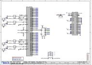
III. MTRX192L test board<br />
The MTRX192L test board is fabricated for the purpose of evaluation and testing of the<br />
MTRX192L <strong>receiver</strong>s. The needed power supplies (+5V, +3.3V and –2V) are fed through the<br />
EMI filters as illustrated in Figure 4. The <strong>receiver</strong> pins are mounted on a pair of clamp fixtures<br />
(the first pair of clamp pins toward the fiber pig-tail direction is not used.) A linear variable<br />
resistor (10kΩ, multi-turns) is mounted on the top of the test board for the adjustment of the V_set<br />
value. Upon shipment, this variable resistor has been adjusted to a nominal position. Users may<br />
adjust this V_set value to optimize the BER performance.<br />
This adjustable V_set configuration is similar to the traditional adjustable decision<br />
threshold and can be very useful in systems (such as DWDM systems) where different<br />
communication channels come with different noise and pulse shape characteristics. When the<br />
V_set value is generated with the system firmware, the <strong>receiver</strong> sensitivity for each channel can<br />
be individually optimized through the system software interface.<br />
3
MTRX192A<br />
MTRX192L<br />
LA<br />
Voutput<br />
500 mV (min.)<br />
p-p<br />
+3.3V -2V<br />
V_ref<br />
V_mon<br />
Figure 1<br />
V_set<br />
Linear Channel<br />
post-amp<br />
F.E<br />
AGC/LA<br />
(A)<br />
∆t ∆t'<br />
(B) (C)<br />
F. E. Output<br />
Figure 2<br />
AGC Amplifier<br />
Limiting Amplifier<br />
Jitter = ∆t(Data)<br />
+ ∆t (LA)<br />
4
+3.3V<br />
(a)<br />
+3.3V<br />
(b)<br />
1K<br />
10K<br />
LM61<br />
20K<br />
V_t<br />
10K<br />
V_set<br />
200<br />
LM385<br />
10K<br />
V_mon<br />
-2V supply<br />
V_set V_t V_ref<br />
100K<br />
100K<br />
6K<br />
100K<br />
100K<br />
Q2<br />
Q3<br />
10K<br />
10K<br />
MAX418<br />
10K<br />
10K<br />
Figure 3<br />
Q1<br />
Q4<br />
10K<br />
10K<br />
10K<br />
0.1µ<br />
(2V)<br />
First pair of clamp pins is not used<br />
Figure 4<br />
V_set probe point<br />
GND<br />
V_pin (+5V)<br />
+3.3V<br />
(Two #1-72 screws to secure the<br />
<strong>receiver</strong> onto the test fixture)<br />
- 2V* (see footnote in P.1)<br />
GND<br />
5
PT4220 Series—48V<br />
10 Watt Low-Profile 48V Input<br />
Isolated DC-DC Converter<br />
SLTS127<br />
(Preliminary 1/17/2001)<br />
Features<br />
• 10W Output Power<br />
• Input Voltage: 36V to 75V<br />
• 1500 VDC Isolation<br />
• Temp Range: –40°C to +85°C<br />
• Remote On/Off Control<br />
• Adjustable Output Voltage<br />
• Undervoltage Lockout<br />
• Current Limit<br />
• Short-Circuit Protection<br />
• Low-Profile Package (8mm)<br />
• Solderable Copper Case<br />
Description<br />
Power Trends’ PT4220 is a new series of<br />
isolated DC-DC Converters housed in an<br />
ultra-low profile (8mm) solderable copper<br />
case. They employ a state-of-the-art high<br />
frequency switch mode topology, and<br />
are available in either a through-hole or<br />
surface-mount package. They are designed<br />
for Telecom, Datacom, Industrial, Computer,<br />
Medical, and other distributed power<br />
applications requiring input-to-output isolation<br />
over an industrial temperature range.<br />
Standard Application<br />
-V in<br />
On/Off V o (adj)<br />
+V in<br />
+V out<br />
5<br />
+Vin<br />
+Vout<br />
8, 9<br />
PT4220<br />
3<br />
-Vin Remote<br />
-Vout<br />
6, 7<br />
Specifications<br />
1<br />
10<br />
L<br />
O<br />
A<br />
D<br />
PT Series Suffix (PT12345X)<br />
Case/Pin<br />
Configuration<br />
Vertical Through-Hole<br />
Horizontal Through-Hole<br />
Horizontal Surface Mount<br />
-V out<br />
(For dimensions and PC board layout,<br />
see Package Styles 1520 and 1530.)<br />
Characteristics<br />
PT4220 SERIES<br />
(Ta=25°C unless noted) Symbols Conditions Min Typ Max Units<br />
Output Current I o Over V in range V o ≤3.3V 0.1 (1) — 3.0<br />
V o =5.0V 0.1 (1) — 2.0 A<br />
V o = 12V 0.1 (1) — 0.85<br />
Short Circuit Current I sc V in = 48V V o ≤ 3.3V — 5.0 —<br />
V o = 5.0V — 4.0 — A<br />
V o =12.0V — 2.0 —<br />
Input Voltage Range V in I o = 0.1 to I omax 36.0 48.0 75.0 V<br />
Set-Point Tolerance V o tol V in =48V, I o =I omax — ±1.0 ±2.0 %Vo<br />
Line Regulation Reg line Over V in range @ max I o — ±1 ±15 mV<br />
Load Regulation Reg load 10% to 100% of I o max — ±5 ±20 mV<br />
V o Temperature Variation Reg temp V in =48V, I o =I omax — ±0.3 — %V o<br />
–40°C ≤ Ta ≤ +85°C<br />
V o Ripple/Noise V n V in=48V, I o= I omax V o ≤5V — 50 —<br />
Vo =12V — 100 — mV pp<br />
Transient Response t tr 50% load change — 75 — µSec<br />
(no output capacitor) V o over/undershoot V o ≤ 5V — 150 — mV<br />
V o =12V — 250 — mV<br />
Efficiency η V in=48V, I o =I omax V o = 1.5V — 71 —<br />
V o = 1.8V — 73 —<br />
V o = 2.5V<br />
V o = 3.3V<br />
—<br />
—<br />
78<br />
81<br />
—<br />
— %<br />
V o = 5.0V — 85 —<br />
V o=12.0V — 87 —<br />
Switching Frequency ƒ o Over V in and I o 250 300 350 kHz<br />
Maximum Operating<br />
Temperature Range<br />
T a Over V in range<br />
-40 — +85 (2) °C<br />
Storage Temperature T s — -40 — 110 °C<br />
Reliability MTBF Per Bellcore TR-332 4.7 — — 10 6 Hrs<br />
50% Stress, 40°C, ground benign<br />
Mechanical Shock — Per Mil-STD-202F, Method 213B,<br />
6mS, Half-sine, mounted to a PCB<br />
— TBD — G’s<br />
Mechanical Vibration — Per Mil-STD-202F, Method 204D,<br />
10-500Hz, Soldered in a PCB<br />
— TBD — G’s<br />
Weight — — 20 — grams<br />
Isolation — Input–output/Input–case 1500 — — V<br />
Capacitance — — 1100 — pF<br />
Resistance — 10 — — MΩ<br />
Flammability — Materials meet UL 94V-0<br />
Remote On/Off On (3) Referenced to –V in 4.5 — —<br />
Off — — 0.8<br />
Notes: (1) The converter will operate down to no load with reduced specifications.<br />
(2) See SOA curves or contact the factory for appropriate derating.<br />
(3) Pin 1 has an internal pull-up and may be driven from an open-collector device. If left open, the converter will<br />
operate when input power is applied. The maximum voltage that may be applied to Pin 1 is 20V.<br />
N<br />
A<br />
C<br />
V<br />
Ordering Information<br />
PT4221r =1.8 Volts<br />
PT4222r =3.3 Volts<br />
PT4223r =5.0 Volts<br />
PT4224r =12.0 Volts<br />
PT4225r =2.5 Volts<br />
PT4226r =1.5 Volts<br />
Pin-Out Information<br />
Pin Function<br />
1<br />
Remote<br />
ON/OFF<br />
2 Do not connect<br />
3 -V in<br />
4 Do not connect<br />
5 +V in<br />
6 -V out<br />
7 -V out<br />
8 +V out<br />
9 +V out<br />
10 V out adjust<br />
For technical support and more information, see inside back cover or visit www.ti.com/powertrends
PT4220 Series—48V<br />
Typical Characteristics<br />
10 Watt Low-Profile 48V Input<br />
Isolated DC-DC Converter<br />
PT4222, V o =3.3VDC (See Note A)<br />
PT4223, Vo =5.0VDC (See Note A)<br />
PT4224, Vo =12.0VDC (See Note A)<br />
90<br />
Efficiency vs Output Current<br />
90<br />
Efficiency vs Output Current<br />
90<br />
Efficiency vs Output Current<br />
Efficiency - %<br />
85<br />
80<br />
75<br />
70<br />
65<br />
VIN<br />
36.0V<br />
48.0V<br />
60.0V<br />
75.0V<br />
Efficiency - %<br />
80<br />
70<br />
60<br />
VIN<br />
36.0V<br />
48.0V<br />
60.0V<br />
75.0V<br />
Efficiency - %<br />
80<br />
70<br />
60<br />
VIN<br />
36.0V<br />
48.0V<br />
60.0V<br />
75.0V<br />
60<br />
0 0.5 1 1.5 2 2.5 3<br />
50<br />
0 0.4 0.8 1.2 1.6 2<br />
50<br />
0 0.2 0.4 0.6 0.8 1<br />
Iout (A)<br />
Iout (A)<br />
Iout (A)<br />
70<br />
Output Ripple vs Output Current<br />
50<br />
Output Ripple vs Output Current<br />
120<br />
Output Ripple vs Output Current<br />
Ripple - mV<br />
60<br />
50<br />
40<br />
30<br />
20<br />
10<br />
VIN<br />
36.0V<br />
48.0V<br />
60.0V<br />
75.0V<br />
Ripple - mV<br />
40<br />
30<br />
20<br />
10<br />
VIN<br />
36.0V<br />
48.0V<br />
60.0V<br />
75.0V<br />
Ripple - mV<br />
100<br />
80<br />
60<br />
40<br />
20<br />
VIN<br />
36.0V<br />
48.0V<br />
60.0V<br />
75.0V<br />
0<br />
0<br />
0<br />
0 0.5 1 1.5 2 2.5 3<br />
0 0.4 0.8 1.2 1.6 2<br />
0 0.2 0.4 0.6 0.8 1<br />
Iout (A)<br />
Iout (A)<br />
Iout (A)<br />
3<br />
Power Dissipation vs Output Current<br />
2<br />
Power Dissipation vs Output Current<br />
1.6<br />
Power Dissipation vs Output Current<br />
Pd - Watts<br />
2.5<br />
2<br />
1.5<br />
1<br />
0.5<br />
VIN<br />
75.0V<br />
60.0V<br />
48.0V<br />
36.0V<br />
Pd - Watts<br />
1.6<br />
1.2<br />
0.8<br />
0.4<br />
VIN<br />
75.0V<br />
60.0V<br />
48.0V<br />
36.0V<br />
Pd - Watts<br />
1.2<br />
0.8<br />
0.4<br />
VIN<br />
75.0V<br />
60.0V<br />
48.0V<br />
36.0V<br />
0<br />
0<br />
0<br />
0 0.5 1 1.5 2 2.5 3<br />
0 0.4 0.8 1.2 1.6 2<br />
0 0.2 0.4 0.6 0.8 1<br />
Iout (A)<br />
Iout (A)<br />
Iout (A)<br />
Safe Operating Area @Vin =48V (Note B)<br />
90.0<br />
Safe Operating Area @Vin =48V (Note B)<br />
90.0<br />
Safe Operating Area @Vin =48V (Note B)<br />
90.0<br />
Ambient Temperature (°C)<br />
80.0<br />
70.0<br />
60.0<br />
50.0<br />
40.0<br />
30.0<br />
Airflow<br />
200LFM<br />
120LFM<br />
60LFM<br />
Nat Conv<br />
Ambient Temperature (°C)<br />
80.0<br />
70.0<br />
60.0<br />
50.0<br />
40.0<br />
30.0<br />
Airflow<br />
200LFM<br />
120LFM<br />
60LFM<br />
Nat Conv<br />
Ambient Temperature (°C)<br />
80.0<br />
70.0<br />
60.0<br />
50.0<br />
40.0<br />
30.0<br />
Airflow<br />
200LFM<br />
120LFM<br />
60LFM<br />
Nat conv<br />
20.0<br />
20.0<br />
20.0<br />
0.0 0.5 1.0 1.5 2.0 2.5 3.0<br />
0.0 0.4 0.8 1.2 1.6 2.0<br />
0.0 0.2 0.4 0.6 0.8 1.0<br />
Iout (A)<br />
Iout (A)<br />
Iout (A)<br />
Note A: All Characteristic data in the above graphs has been developed from actual products tested at 25°C. This data is considered typical data for the converter.<br />
Note B: SOA curves represent operating conditions at which internal components are at or below manufacturer’s maximum rated operating temperatures.<br />
For technical support and more information, see inside back cover or visit www.ti.com/powertrends
Application Notes<br />
PT4220/4240 Series<br />
Adjusting the Output Voltage of the 10W<br />
Excalibur Series of Isolated DC-DC Converters<br />
The factory pre-set output voltage of Power Trends’ 10W<br />
Excalibur series of isolated DC-DC converters may be<br />
adjusted over a narrow range. This is accomplished with<br />
the addition of a single external resistor. For the input<br />
voltage range specified in the data sheet, Table 1 gives the<br />
allowable adjustment range for each model as V o (min)<br />
and V o (max).<br />
Adjust Up: An increase in the output voltage is obtained<br />
by adding a resistor, R 2 between pin 10 (V o adjust), and<br />
pins 6 & 7 (–V out ).<br />
Adjust Down: Add a resistor (R 1 ), between pin 10 (V o adjust)<br />
and pins 8 & 9 (+V out ).<br />
Refer to Figure 1 and Table 2 for both the placement and value<br />
of the required resistor, (R 1 ) or R 2 .<br />
1. Use only a single 1% resistor in either the (R 1 ) or R 2<br />
location. Place the resistor as close to the ISR as possible.<br />
2. Never connect capacitors to V o adjust. Any capacitance<br />
added to the V o adjust control pin will affect the stability of<br />
the ISR. The values of (R 1 ) [adjust down], and R 2 [adjust<br />
up], can also be calculated using the following formulas.<br />
(R 1 ) = 56.2 (V a – 1.225) – R s kΩ<br />
V o – V a<br />
R 2 =<br />
68.845<br />
V a – V o<br />
– R s kΩ<br />
Where, V o = Original output voltage<br />
V a = Adjusted output voltage<br />
R s = Series resistance (Table 1)<br />
Notes:<br />
Table 1<br />
DC-DC CONVERTER ADJUSTMENT RANGE AND FORMULA PARAMETERS<br />
Series Pt #<br />
24V Bus PT4246 PT4241 PT4245 PT4242 PT4243 PT4244<br />
48V Bus PT4226 PT4221 PT4225 PT4222 PT4223 PT4224<br />
Vo(nom) 1.5V 1.8V 2.5V 3.3V 5.0V 12.0V<br />
Vo(min) 1.45V 1.7V 2.25V 2.95V 4.5V 10.8V<br />
Vo(max) 1.65V 1.98V 2.75V 3.65V 5.5V 13.2V<br />
Rs (kΩ) 243.0 243.0 187.0 187.0 110.0 49.9<br />
Figure 1<br />
+V in<br />
-V in<br />
3<br />
6, 7<br />
-Vin<br />
-Vout<br />
(R1)<br />
Remote<br />
On/Off<br />
V o<br />
(adj)<br />
5<br />
+Vin<br />
+Vout<br />
8, 9<br />
+V O<br />
PT4220/4240<br />
1<br />
10<br />
R2<br />
Adjust Up<br />
L<br />
O<br />
A<br />
D<br />
–V O<br />
For technical support and more information, see inside back cover or visit www.ti.com/powertrends
Application Notes continued<br />
PT4220/4240 Series<br />
Table 2<br />
DC-DC CONVERTER ADJUSTMENT RESISTOR VALUES<br />
Series Pt #<br />
24V Bus PT4246 PT4241 PT4245 PT4242 PT4243 PT4244<br />
48V Bus PT4226 PT4221 PT4225 PT4222 PT4223 PT4224<br />
Vo(nom) 1.5V 1.8V 2.5V 3.3V 5.0V 12.0V<br />
V a (req’d)<br />
V a (req’d)<br />
1.45 (9.9)kΩ<br />
1.5<br />
1.55 1130.0kΩ<br />
1.6 445.0kΩ<br />
1.65 216.0kΩ<br />
1.7 (23.9)kΩ<br />
1.75 (347.0)kΩ<br />
1.8<br />
1.85 1130.0kΩ<br />
1.9 445.0kΩ<br />
1.95 216.0kΩ<br />
2.25 (43.4)kΩ<br />
2.3 (115.0)kΩ<br />
2.35 (235.0)kΩ<br />
2.4 (473.0)kΩ<br />
2.45 (1190.0)kΩ<br />
2.5<br />
2.55 1190.0kΩ<br />
2.6 501.0kΩ<br />
2.65 272.0kΩ<br />
2.7 157.0kΩ<br />
2.75 88.4kΩ<br />
2.95 (90.0)kΩ<br />
3.0 (146.0)kΩ<br />
3.05 (223.0)kΩ<br />
3.1 (340.0)kΩ<br />
3.15 (534.0)kΩ<br />
3.2 (923.0)kΩ<br />
3.25 (2090.0)kΩ<br />
3.3<br />
3.35 1190.0kΩ<br />
3.4 501.0kΩ<br />
3.45 272.0kΩ<br />
3.5 157.0kΩ<br />
3.55 88.4kΩ<br />
3.6 42.5kΩ<br />
3.65 9.7kΩ<br />
R1 = (Blue)<br />
R2 = Black<br />
4.5 (258.0)kΩ<br />
4.6 (364.0)kΩ<br />
4.7 (541.0)kΩ<br />
4.8 (895.0)kΩ<br />
4.9 (1960.0)kΩ<br />
5.0<br />
5.1 578.0kΩ<br />
5.2 234.0kΩ<br />
5.3 119.0kΩ<br />
5.4 62.1kΩ<br />
5.5 27.7kΩ<br />
10.8 (399.0)kΩ<br />
11.0 (499.0)kΩ<br />
11.5 (1110.0)kΩ<br />
12.0<br />
12.5 87.8kΩ<br />
13.0 18.9kΩ<br />
13.2 7.5kΩ<br />
For technical support and more information, see inside back cover or visit www.ti.com/powertrends
Application Notes<br />
PT4220/4240 Series<br />
Using the Inhibit Function on the PT4220/4240<br />
Isolated 10W Excalibur DC/DC Converters<br />
Applications requiring output voltage On/Off control, the<br />
PT4220/4240 DC/DC converter series incorporates a<br />
“Remote On/Off” control (pin 1). This feature can be<br />
used when there is a requirement for the module to be<br />
switched off without removing the applied input source<br />
voltage.<br />
The converter functions normally with Pin 1 open-circuit,<br />
providing a regulated output voltage when a valid source<br />
voltage is applied to +V in (pin 5), with respect to –V in<br />
(pin 3). When a low-level 1 ground signal is applied to<br />
pin 1, the converter output will be turned off.<br />
Figure 1 shows an application schematic, which details<br />
the typical use of the Remote On/Off function. Note the<br />
discrete transistor (Q1). The control pin has its own<br />
internal pull-up, allowing the pin to be controlled with<br />
an open-collector or open-drain device (See notes 2 & 3).<br />
Table 1 gives the threshold requirements.<br />
When placed in the “Off” state, the standby current drawn<br />
from the input source is typically reduced to less than 1mA.<br />
Table 1; Pin 1 Remote On/Off Control Parameters 1<br />
Parameter Min Typ Max<br />
Enable (VIH) 4.5V — —<br />
Disable (VIL) — — 0.8V<br />
Von [Open-Circuit] 5.0V<br />
Ioff [pin 1 at –Vin] — — –0.5mA<br />
Notes:<br />
1. The Remote On/Off control uses –V in (pin 3) as its ground<br />
reference. All voltages specified are with respect to –V in .<br />
2. Use an open-collector device (preferably a discrete<br />
transistor) for the Remote On/Off input. A pull-up resistor<br />
is not necessary. To disable the output voltage, the control<br />
pin should be pulled low to less than +0.8VDC.<br />
3. The Remote On/Off pin may be controlled with devices that<br />
have a totem-pole output. This is provided the drive<br />
voltage meets the threshold requirements in Table 1.<br />
Do not apply more than +20V. If a TTL gate is used, a<br />
pull-up resistor may be required to the logic supply voltage.<br />
4. The PT4220/4240 converters incorporate an “Under-<br />
Voltage Lockout” (UVLO). The UVLO will override<br />
pin 1, and keep the module off when the input voltage to<br />
the converter is low. Table 2 gives the UVLO input<br />
voltage thresholds.<br />
Figure 1<br />
+V in<br />
-V in<br />
1 =OFF<br />
Vdd<br />
Turn-On Time: In the circuit of Figure 1, turning Q 1 on applies<br />
a low-voltage to pin 1 and disables the converter output.<br />
Correspondingly, turning Q 1 off allows pin 1 to be pulled<br />
high by an internal pull-up resistor. The converter produces a<br />
regulated output voltage within 60 milli-secs. Although the<br />
rise-time of the output is short (
Application Notes—AN20<br />
Isolated Products<br />
Using the PT4200/4205/4300 DC to DC Converter<br />
Remote Control (RC) Turn-on or turn-off can be realized<br />
by using the RC pin. Normal operation is achieved if pin 11<br />
is open. If pin 11 is connected to pin 17 (PT4200/4300) or<br />
pin 18 (PT4205), the power module turns off. To insure safe<br />
turn-off, the voltage difference between pin 11 and 17 or 18<br />
should be less than 1.0V. RC is compatible with TTL open<br />
collector outputs with a sink capacity > 300µA (see figure<br />
28).<br />
Figure 28<br />
PT4200/4205/4300 REMOTE CONTROL<br />
TTL<br />
RC (pin 11)<br />
(pin 17 for PT4200)<br />
-In<br />
(pin 18 for PT4205)<br />
Over Voltage Protection (OVP) The remote control can<br />
also be utilized for OVP by using the external circuitry<br />
shown in figure 29. Resistor values are for 5V output applications,<br />
but can easily be adjusted for other output voltages<br />
and the desired OVP level.<br />
Figure 29<br />
PT4200/4205/4300 OVER VOLTAGE PROTECTION<br />
Out 1 (pin 1)<br />
Rtn (pin 2)<br />
15K<br />
10K<br />
1K<br />
1K<br />
TL431<br />
270<br />
RC (pin 11)<br />
(pin 17 for PT4200)<br />
-In<br />
(pin 18 for PT4205)<br />
Turn-on/off Input Voltage The power module monitors the<br />
input voltage and will turn on and turn off at predetermined<br />
levels set by means of external resistors.<br />
To increase V Ion<br />
connect a resistor between pin 11 and 17<br />
(PT4200/4300) or 18 (PT4205) (see figure 30). The<br />
resistance is determined by the following equations; (a)<br />
PT4200/4300, (b) PT4205:<br />
(a) R Ion<br />
= 100 x (100.2 - V Ion<br />
)/(V Ion<br />
- 36.5) kΩ (for V Ion<br />
>37V)<br />
(b) R Ion<br />
= 1000 x (1110 - V Ion<br />
)/(V Ion<br />
- 18.7) kΩ (for V Ion<br />
>18.7V)<br />
where 18.7 or 36.5 is the typical unadjusted turn-on input<br />
voltage. V Ioff<br />
is the adjusted turn-off input voltage and is<br />
determined by V Ion<br />
-V Ioff<br />
= 2V (typical value).<br />
To decrease V Ion<br />
connect a resistor between pin 10 and 11<br />
(see figure 30). The resistance is determined by the<br />
following equations; (a) PT4200/4300, (b) PT4205:<br />
(a) R Ion = 364 x (V Ion -29.9)/(36.5 -V Ion) kΩ (for 30
IMPORTANT NOTICE<br />
Texas Instrum ents and its subsidiaries (TI) reserve the right to m ake changes to their products or to discontinue<br />
any product or service without notice, and advise custom ers to obtain the latest version of relevant inform ation<br />
to verify, before placing orders, that inform ation being relied on is current and com plete. All products are sold<br />
subject to the term s and conditions of sale supplied at the tim e of order acknowledgm ent, including those<br />
pertaining to warranty, patent infringem ent, and lim itation of liability.<br />
TI warrants perform ance of its sem iconductor products to the specifications applicable at the tim e of sale in<br />
accordance with TI’s standard warranty. Testing and other quality control techniques are utilized to the extent<br />
TI deem s necessary to support this warranty. Specific testing of all param eters of each device is not necessarily<br />
perform ed, except those m andated by governm ent requirem ents.<br />
Custom ers are responsible for their applications using TI com ponents.<br />
In order to m inim ize risks associated with the custom er’s applications, adequate design and operating<br />
safeguards m ust be provided by the custom er to m inim ize inherent or procedural hazards.<br />
TI assum es no liability for applications assistance or custom er product design. TI does not warrant or represent<br />
that any license, either express or im plied, is granted under any patent right, copyright, m ask work right, or other<br />
intellectual property right of TI covering or relating to any com bination, m achine, or process in which such<br />
sem iconductor products or services m ight be or are used. TI’s publication of inform ation regarding any third<br />
party’s products or services does not constitute TI’s approval, warranty or endorsem ent thereof.<br />
Copyright © 2000, Texas Instrum ents Incorporated
The MC78L00A Series of positive voltage regulators are<br />
inexpensive, easy–to–use devices suitable for a multitude of<br />
applications that require a regulated supply of up to 100 mA. Like<br />
their higher powered MC7800 and MC78M00 Series cousins, these<br />
regulators feature internal current limiting and thermal shutdown<br />
making them remarkably rugged. No external components are<br />
required with the MC78L00 devices in many applications.<br />
These devices offer a substantial performance advantage over the<br />
traditional zener diode–resistor combination, as output impedance<br />
and quiescent current are substantially reduced.<br />
• Wide Range of Available, Fixed Output Voltages<br />
• Low Cost<br />
• Internal Short Circuit Current Limiting<br />
• Internal Thermal Overload Protection<br />
• No External Components Required<br />
• Complementary Negative Regulators Offered (MC79L00A Series)<br />
<br />
<br />
<br />
<br />
<br />
<br />
<br />
Representative Schematic Diagram<br />
<br />
<br />
<br />
<br />
µ<br />
<br />
<br />
<br />
<br />
<br />
<br />
<br />
<br />
<br />
Standard Application<br />
<br />
<br />
<br />
<br />
<br />
<br />
<br />
<br />
<br />
<br />
<br />
<br />
1<br />
2<br />
8<br />
V OUT<br />
http://onsemi.com<br />
3<br />
GND<br />
GND<br />
NC<br />
Pin: 1. Output<br />
2. Ground<br />
3. Input<br />
1<br />
TO–92<br />
P SUFFIX<br />
CASE 029<br />
PIN CONNECTIONS<br />
1 8<br />
2<br />
7<br />
3<br />
6<br />
4<br />
5<br />
(Top View)<br />
SOP–8*<br />
D SUFFIX<br />
CASE 751<br />
*SOP–8 is an internally modified SO–8 package. Pins<br />
2, 3, 6, and 7 are electrically common to the die attach<br />
flag. This internal lead frame modification decreases<br />
package thermal resistance and increases power<br />
dissipation capability when appropriately mounted on<br />
a printed circuit board. SOP–8 conforms to all external<br />
dimensions of the standard SO–8 package.<br />
V IN<br />
GND<br />
GND<br />
NC<br />
ORDERING INFORMATION<br />
See detailed ordering and shipping information in the package<br />
dimensions section on page 8 of this data sheet.<br />
DEVICE MARKING INFORMATION<br />
See general marking information in the device marking<br />
section on page 10 of this data sheet.<br />
A common ground is required between the input and the output voltages. The<br />
input voltage must remain typically 2.0 V above the output voltage even during<br />
the low point on the input ripple voltage.<br />
*C in is required if regulator is located an appreciable distance from power<br />
supply filter.<br />
** C O is not needed for stability; however, it does improve transient response.<br />
© Semiconductor Components Industries, LLC, 2000<br />
October, 2000 – Rev. 1<br />
1 Publication Order Number:<br />
MC78L00A/D
MC78L00A Series<br />
MAXIMUM RATINGS (T A = +125°C, unless otherwise noted.)<br />
Rating Symbol Value Unit<br />
Input Voltage (2.6 V–8.0 V)<br />
Input Voltage (12 V–18 V)<br />
Input Voltage (24 V)<br />
V I 30<br />
35<br />
40<br />
Storage Temperature Range T stg –65 to +150 °C<br />
Operating Junction Temperature Range T J 0 to +150 °C<br />
Vdc<br />
ELECTRICAL CHARACTERISTICS (V I = 10 V, I O = 40 mA, C I = 0.33 µF, C O = 0.1 µF, –40°C < T J < +125°C (for MC78LXXAB),<br />
0°C < T J < +125°C (for MC78LXXAC), unless otherwise noted.)<br />
MC78L05AC, AB<br />
Characteristics Symbol Min Typ Max Unit<br />
Output Voltage (T J = +25°C) V O 4.8 5.0 5.2 Vdc<br />
Line Regulation<br />
(T J = +25°C, I O = 40 mA)<br />
7.0 Vdc ≤ V I ≤ 20 Vdc<br />
8.0 Vdc ≤ V I ≤ 20 Vdc<br />
Reg line<br />
–<br />
–<br />
55<br />
45<br />
150<br />
100<br />
mV<br />
Load Regulation<br />
(T J = +25°C, 1.0 mA ≤ I O ≤ 100 mA)<br />
(T J = +25°C, 1.0 mA ≤ I O ≤ 40 mA)<br />
Output Voltage<br />
(7.0 Vdc ≤ V I ≤ 20 Vdc, 1.0 mA ≤ I O ≤ 40 mA)<br />
(V I = 10 V, 1.0 mA ≤ I O ≤ 70 mA)<br />
Input Bias Current<br />
(T J = +25°C)<br />
(T J = +125°C)<br />
Input Bias Current Change<br />
(8.0 Vdc ≤ V I ≤ 20 Vdc)<br />
(1.0 mA ≤ I O ≤ 40 mA)<br />
Output Noise Voltage<br />
(T A = +25°C, 10 Hz ≤ f ≤ 100 kHz)<br />
Ripple Rejection (I O = 40 mA,<br />
f = 120 Hz, 8.0 Vdc ≤ V I ≤ 18 V, T J = +25°C)<br />
Reg load<br />
–<br />
–<br />
V O<br />
4.75<br />
4.75<br />
I IB<br />
–<br />
–<br />
∆I IB<br />
–<br />
–<br />
11<br />
5.0<br />
–<br />
–<br />
3.8<br />
–<br />
–<br />
–<br />
60<br />
30<br />
5.25<br />
5.25<br />
6.0<br />
5.5<br />
1.5<br />
0.1<br />
mV<br />
Vdc<br />
mA<br />
mA<br />
V n – 40 – µV<br />
RR 41 49 – dB<br />
Dropout Voltage (T J = +25°C) V I – V O – 1.7 – Vdc<br />
http://onsemi.com<br />
2
MC78L00A Series<br />
ELECTRICAL CHARACTERISTICS (V I = 14 V, I O = 40 mA, C I = 0.33 µF, C O = 0.1 µF, –40°C < T J < +125°C (for MC78LXXAB),<br />
0°C < T J < +125°C (for MC78LXXAC), unless otherwise noted.)<br />
MC78L08AC, AB<br />
Characteristics Symbol Min Typ Max Unit<br />
Output Voltage (T J = +25°C) V O 7.7 8.0 8.3 Vdc<br />
Line Regulation<br />
(T J = +25°C, I O = 40 mA)<br />
10.5 Vdc ≤ V I ≤ 23 Vdc<br />
11 Vdc ≤ V I ≤ 23 Vdc<br />
Reg line<br />
–<br />
–<br />
20<br />
12<br />
175<br />
125<br />
mV<br />
Load Regulation<br />
(T J = +25°C, 1.0 mA ≤ I O ≤ 100 mA)<br />
(T J = +25°C, 1.0 mA ≤ I O ≤ 40 mA)<br />
Output Voltage<br />
(10.5 Vdc ≤ V I ≤ 23 Vdc, 1.0 mA ≤ I O ≤ 40 mA)<br />
(V I = 14 V, 1.0 mA ≤ I O ≤ 70 mA)<br />
Input Bias Current<br />
(T J = +25°C)<br />
(T J = +125°C)<br />
Input Bias Current Change<br />
(11 Vdc ≤ V I ≤ 23 Vdc)<br />
(1.0 mA ≤ I O ≤ 40 mA)<br />
Output Noise Voltage<br />
(T A = +25°C, 10 Hz ≤ f ≤ 100 kHz)<br />
Ripple Rejection (I O = 40 mA,<br />
f = 120 Hz, 12 V ≤ V I ≤ 23 V, T J = +25°C)<br />
Reg load<br />
–<br />
–<br />
V O<br />
7.6<br />
7.6<br />
I IB<br />
–<br />
–<br />
∆I IB<br />
–<br />
–<br />
15<br />
8.0<br />
–<br />
–<br />
3.0<br />
–<br />
–<br />
–<br />
80<br />
40<br />
8.4<br />
8.4<br />
6.0<br />
5.5<br />
1.5<br />
0.1<br />
mV<br />
Vdc<br />
mA<br />
mA<br />
V n – 60 – µV<br />
RR 37 57 – dB<br />
Dropout Voltage (T J = +25°C) V I – V O – 1.7 – Vdc<br />
ELECTRICAL CHARACTERISTICS (V I = 15 V, I O = 40 mA, C I = 0.33 µF, C O = 0.1 µF, –40°C < T J < +125°C (for MC78LXXAB),<br />
0°C < T J < +125°C (for MC78LXXAC), unless otherwise noted.)<br />
MC78L09AC, AB<br />
Characteristics Symbol Min Typ Max Unit<br />
Output Voltage (T J = +25°C) V O 8.6 9.0 9.4 Vdc<br />
Line Regulation<br />
(T J = +25°C, I O = 40 mA)<br />
11.5 Vdc ≤ V I ≤ 24 Vdc<br />
12 Vdc ≤ V I ≤ 24 Vdc<br />
Load Regulation<br />
(T J = +25°C, 1.0 mA ≤ I O ≤ 100 mA)<br />
(T J = +25°C, 1.0 mA ≤ I O ≤ 40 mA)<br />
Output Voltage<br />
(11.5 Vdc ≤ V I ≤ 24 Vdc, 1.0 mA ≤ I O ≤ 40 mA)<br />
(V I = 15 V, 1.0 mA ≤ I O ≤ 70 mA)<br />
Input Bias Current<br />
(T J = +25°C)<br />
(T J = +125°C)<br />
Input Bias Current Change<br />
(11 Vdc ≤ V I ≤ 23 Vdc)<br />
(1.0 mA ≤ I O ≤ 40 mA)<br />
Output Noise Voltage<br />
(T A = +25°C, 10 Hz ≤ f ≤ 100 kHz)<br />
Ripple Rejection (I O = 40 mA,<br />
f = 120 Hz, 13 V ≤ V I ≤ 24 V, T J = +25°C)<br />
Dropout Voltage<br />
(T J = +25°C)<br />
Reg line<br />
–<br />
–<br />
Reg load<br />
–<br />
–<br />
V O<br />
8.5<br />
8.5<br />
I IB<br />
–<br />
–<br />
∆I IB<br />
–<br />
–<br />
20<br />
12<br />
15<br />
8.0<br />
–<br />
–<br />
3.0<br />
–<br />
–<br />
–<br />
175<br />
125<br />
90<br />
40<br />
9.5<br />
9.5<br />
6.0<br />
5.5<br />
1.5<br />
0.1<br />
mV<br />
mV<br />
Vdc<br />
mA<br />
mA<br />
V n – 60 – µV<br />
RR 37 57 – dB<br />
V I – V O – 1.7 – Vdc<br />
http://onsemi.com<br />
3
MC78L00A Series<br />
ELECTRICAL CHARACTERISTICS (V I = 19 V, I O = 40 mA, C I = 0.33 µF, C O = 0.1 µF, –40°C < T J < +125°C (for MC78LXXAB),<br />
0°C < T J < +125°C (for MC78LXXAC), unless otherwise noted.)<br />
MC78L12AC, AB<br />
Characteristics Symbol Min Typ Max Unit<br />
Output Voltage (T J = +25°C) V O 11.5 12 12.5 Vdc<br />
Line Regulation<br />
(T J = +25°C, I O = 40 mA)<br />
14.5 Vdc ≤ V I ≤ 27 Vdc<br />
16 Vdc ≤ V I ≤ 27 Vdc<br />
Load Regulation<br />
(T J = +25°C, 1.0 mA ≤ I O ≤ 100 mA)<br />
(T J = +25°C, 1.0 mA ≤ I O ≤ 40 mA)<br />
Output Voltage<br />
(14.5 Vdc ≤ V I ≤ 27 Vdc, 1.0 mA ≤ I O ≤ 40 mA)<br />
(V I = 19 V, 1.0 mA ≤ I O ≤ 70 mA)<br />
Input Bias Current<br />
(T J = +25°C)<br />
(T J = +125°C)<br />
Input Bias Current Change<br />
(16 Vdc ≤ V I ≤ 27 Vdc)<br />
(1.0 mA ≤ I O ≤ 40 mA)<br />
Output Noise Voltage<br />
(T A = +25°C, 10 Hz ≤ f ≤ 100 kHz)<br />
Reg line<br />
–<br />
–<br />
Reg load<br />
–<br />
–<br />
V O<br />
11.4<br />
11.4<br />
I IB<br />
–<br />
–<br />
∆I IB<br />
–<br />
–<br />
120<br />
100<br />
20<br />
10<br />
–<br />
–<br />
4.2<br />
–<br />
–<br />
–<br />
250<br />
200<br />
100<br />
50<br />
12.6<br />
12.6<br />
6.5<br />
6.0<br />
1.5<br />
0.1<br />
mV<br />
mV<br />
Vdc<br />
mA<br />
mA<br />
V n – 80 – µV<br />
Ripple Rejection (I O = 40 mA,<br />
f = 120 Hz, 15 V ≤ V I ≤ 25 V, T J = +25°C)<br />
Dropout Voltage<br />
(T J = +25°C)<br />
RR 37 42 – dB<br />
V I – V O – 1.7 – Vdc<br />
ELECTRICAL CHARACTERISTICS (V I = 23 V, I O = 40 mA, C I = 0.33 µF, C O = 0.1 µF, –40°C < T J < +125°C (for MC78LXXAB),<br />
S 0°C < T J < +125°C (for MC78LXXAC), unless otherwise noted.)<br />
MC78L15AC, AB<br />
Characteristics Symbol Min Typ Max Unit<br />
Output Voltage (T J = +25°C) V O 14.4 15 15.6 Vdc<br />
Line Regulation<br />
(T J = +25°C, I O = 40 mA)<br />
17.5 Vdc ≤ V I ≤ 30 Vdc<br />
20 Vdc ≤ V I ≤ 30 Vdc<br />
Reg line<br />
–<br />
–<br />
130<br />
110<br />
300<br />
250<br />
mV<br />
Load Regulation<br />
(T J = +25°C, 1.0 mA ≤ I O ≤ 100 mA)<br />
(T J = +25°C, 1.0 mA ≤ I O ≤ 40 mA)<br />
Output Voltage<br />
(17.5 Vdc ≤ V I ≤ 30 Vdc, 1.0 mA ≤ I O ≤ 40 mA)<br />
(V I = 23 V, 1.0 mA ≤ I O ≤ 70 mA)<br />
Input Bias Current<br />
(T J = +25°C)<br />
(T J = +125°C)<br />
Input Bias Current Change<br />
(20 Vdc ≤ V I ≤ 30 Vdc)<br />
(1.0 mA ≤ I O ≤ 40 mA)<br />
Output Noise Voltage<br />
(T A = +25°C, 10 Hz ≤ f ≤ 100 kHz)<br />
Ripple Rejection (I O = 40 mA,<br />
f = 120 Hz, 18.5 V ≤ V I ≤ 28.5 V, T J = +25°C)<br />
Dropout Voltage<br />
(T J = +25°C)<br />
Reg load<br />
–<br />
–<br />
V O<br />
14.25<br />
14.25<br />
I IB<br />
–<br />
–<br />
∆I IB<br />
–<br />
–<br />
25<br />
12<br />
–<br />
–<br />
4.4<br />
–<br />
–<br />
–<br />
150<br />
75<br />
15.75<br />
15.75<br />
6.5<br />
6.0<br />
1.5<br />
0.1<br />
mV<br />
Vdc<br />
mA<br />
mA<br />
V n – 90 – µV<br />
RR 34 39 – dB<br />
V I – V O – 1.7 – Vdc<br />
http://onsemi.com<br />
4
MC78L00A Series<br />
ELECTRICAL CHARACTERISTICS (V I = 27 V, I O = 40 mA, C I = 0.33 µF, C O = 0.1 µF, 0°C < T J < +125°C, unless otherwise noted.)<br />
MC78L18AC<br />
Characteristics Symbol Min Typ Max Unit<br />
Output Voltage (T J = +25°C) V O 17.3 18 18.7 Vdc<br />
Line Regulation<br />
(T J = +25°C, I O = 40 mA)<br />
21.4 Vdc ≤ V I ≤ 33 Vdc<br />
20.7 Vdc ≤ V I ≤ 33 Vdc<br />
22 Vdc ≤ V I ≤ 33 Vdc<br />
21 Vdc ≤ V I ≤ 33 Vdc<br />
Load Regulation<br />
(T J = +25°C, 1.0 mA ≤ I O ≤ 100 mA)<br />
(T J = +25°C, 1.0 mA ≤ I O ≤ 40 mA)<br />
Output Voltage<br />
(21.4 Vdc ≤ V I ≤ 33 Vdc, 1.0 mA ≤ I O ≤ 40 mA)<br />
(20.7 Vdc ≤ V I ≤ 33 Vdc, 1.0 mA ≤ I O ≤ 40 mA)<br />
(V I = 27 V, 1.0 mA ≤ I O ≤ 70 mA)<br />
(V I = 27 V, 1.0 mA ≤ I O ≤ 70 mA)<br />
Input Bias Current<br />
(T J = +25°C)<br />
(T J = +125°C)<br />
Input Bias Current Change<br />
(22 Vdc ≤ V I ≤ 33 Vdc)<br />
(21 Vdc ≤ V I ≤ 33 Vdc)<br />
(1.0 mA ≤ I O ≤ 40 mA)<br />
Output Noise Voltage<br />
(T A = +25°C, 10 Hz ≤ f ≤ 100 kHz)<br />
Ripple Rejection (I O = 40 mA,<br />
f = 120 Hz, 23 V ≤ V I ≤ 33 V, T J = +25°C)<br />
Dropout Voltage<br />
(T J = +25°C)<br />
Reg line –<br />
–<br />
Reg load<br />
–<br />
–<br />
V O<br />
17.1<br />
17.1<br />
I IB<br />
–<br />
–<br />
∆I IB<br />
–<br />
–<br />
45<br />
35<br />
30<br />
15<br />
–<br />
–<br />
3.1<br />
–<br />
–<br />
–<br />
325<br />
275<br />
170<br />
85<br />
18.9<br />
18.9<br />
6.5<br />
6.0<br />
1.5<br />
0.1<br />
mV<br />
mV<br />
Vdc<br />
mA<br />
mA<br />
V n – 150 – µV<br />
RR 33 48 – dB<br />
V I – V O – 1.7 – Vdc<br />
ELECTRICAL CHARACTERISTICS (V I = 33 V, I O = 40 mA, C I = 0.33 µF, C O = 0.1 µF, 0°C < T J < +125°C, unless otherwise noted.)<br />
MC78L24AC<br />
Characteristics Symbol Min Typ Max Unit<br />
Output Voltage (T J = +25°C) V O 23 24 25 Vdc<br />
Line Regulation<br />
(T J = +25°C, I O = 40 mA)<br />
27.5 Vdc ≤ V I ≤ 38 Vdc<br />
28 Vdc ≤ V I ≤ 80 Vdc<br />
27 Vdc ≤ V I ≤ 38 Vdc<br />
Reg line<br />
–<br />
–<br />
–<br />
–<br />
50<br />
60<br />
–<br />
300<br />
350<br />
mV<br />
Load Regulation<br />
(T J = +25°C, 1.0 mA ≤ I O ≤ 100 mA)<br />
(T J = +25°C, 1.0 mA ≤ I O ≤ 40 mA)<br />
Output Voltage<br />
(28 Vdc ≤ V I ≤ 38 Vdc, 1.0 mA ≤ I O ≤ 40 mA)<br />
(27 Vdc ≤ V I ≤ 38 Vdc, 1.0 mA ≤ I O ≤ 40 mA)<br />
(28 Vdc ≤ V I = 33 Vdc, 1.0 mA ≤ I O ≤ 70 mA)<br />
(27 Vdc ≤ V I ≤ 33 Vdc, 1.0 mA ≤ I O ≤ 70 mA)<br />
Input Bias Current<br />
(T J = +25°C)<br />
(T J = +125°C)<br />
Input Bias Current Change<br />
(28 Vdc ≤ V I ≤ 38 Vdc)<br />
(1.0 mA ≤ I O ≤ 40 mA)<br />
Output Noise Voltage<br />
(T A = +25°C, 10 Hz ≤ f ≤ 100 kHz)<br />
Ripple Rejection (I O = 40 mA,<br />
f = 120 Hz, 29 V ≤ V I ≤ 35 V, T J = +25°C)<br />
Dropout Voltage<br />
(T J = +25°C)<br />
Reg load<br />
–<br />
–<br />
V O<br />
22.8<br />
22.8<br />
I IB<br />
–<br />
–<br />
∆I IB<br />
–<br />
–<br />
40<br />
20<br />
–<br />
–<br />
3.1<br />
–<br />
–<br />
–<br />
200<br />
100<br />
25.2<br />
25.2<br />
6.5<br />
6.0<br />
1.5<br />
0.1<br />
mV<br />
Vdc<br />
mA<br />
mA<br />
V n – 200 – µV<br />
RR 31 45 – dB<br />
V I – V O – 1.7 – Vdc<br />
http://onsemi.com<br />
5
MC78L00A Series<br />
<br />
<br />
<br />
<br />
<br />
<br />
<br />
<br />
<br />
<br />
<br />
<br />
<br />
<br />
<br />
°<br />
<br />
<br />
<br />
Figure 1. Dropout Characteristics<br />
<br />
<br />
<br />
<br />
<br />
<br />
°<br />
Figure 3. Input Bias Current versus<br />
Ambient Temperature<br />
<br />
<br />
<br />
<br />
<br />
<br />
<br />
<br />
<br />
<br />
<br />
<br />
<br />
°<br />
<br />
<br />
<br />
<br />
<br />
<br />
<br />
Figure 2. Dropout Voltage versus<br />
Junction Temperature<br />
<br />
<br />
<br />
°<br />
<br />
<br />
<br />
<br />
Figure 4. Input Bias Current<br />
versus Input Voltage<br />
<br />
<br />
<br />
<br />
θ °<br />
°<br />
<br />
<br />
<br />
°<br />
Figure 5. Maximum Average Power Dissipation versus<br />
Ambient Temperature – TO–92 Type Package<br />
θ °<br />
<br />
<br />
<br />
<br />
°<br />
<br />
<br />
<br />
ÎÎÎ<br />
ÎÎÎ ÎÎÎ<br />
<br />
<br />
<br />
ÎÎÎ<br />
ÎÎÎ ÎÎÎ<br />
<br />
<br />
<br />
<br />
<br />
<br />
θ<br />
<br />
<br />
<br />
<br />
ÎÎÎ<br />
ÎÎÎ<br />
Figure 6. SOP–8 Thermal Resistance and Maximum<br />
Power Dissipation versus P.C.B. Copper Length<br />
<br />
<br />
<br />
<br />
<br />
<br />
http://onsemi.com<br />
6
MC78L00A Series<br />
APPLICATIONS INFORMATION<br />
Design Considerations<br />
The MC78L00A Series of fixed voltage regulators are<br />
designed with Thermal Overload Protection that shuts<br />
down the circuit when subjected to an excessive power<br />
overload condition. Internal Short Circuit Protection limits<br />
the maximum current the circuit will pass.<br />
In many low current applications, compensation<br />
capacitors are not required. However, it is recommended<br />
that the regulator input be bypassed with a capacitor if the<br />
regulator is connected to the power supply filter with long<br />
wire lengths, or if the output load capacitance is large. The<br />
input bypass capacitor should be selected to provide good<br />
high–frequency characteristics to insure stable operation<br />
under all load conditions. A 0.33 µF or larger tantalum,<br />
mylar, or other capacitor having low internal impedance at<br />
high frequencies should be chosen. The bypass capacitor<br />
should be mounted with the shortest possible leads directly<br />
across the regulators input terminals. Good construction<br />
techniques should be used to minimize ground loops and<br />
lead resistance drops since the regulator has no external<br />
sense lead. Bypassing the output is also recommended.<br />
<br />
µ<br />
<br />
<br />
<br />
<br />
<br />
<br />
<br />
<br />
<br />
<br />
<br />
µ<br />
µ<br />
<br />
<br />
<br />
<br />
<br />
<br />
<br />
<br />
<br />
<br />
Figure 8. ± 15 V Tracking Voltage Regulator<br />
<br />
<br />
<br />
<br />
<br />
<br />
<br />
<br />
<br />
<br />
<br />
<br />
<br />
µ<br />
µ<br />
<br />
Ω<br />
<br />
<br />
µ<br />
<br />
µ<br />
<br />
Figure 7. Current Regulator<br />
Figure 9. Positive and Negative Regulator<br />
http://onsemi.com<br />
7
MC78L00A Series<br />
Device<br />
Output Voltage<br />
ORDERING INFORMATION<br />
Operating<br />
Temperature Range Package Shipping<br />
MC78L05ABD SOP–8 98 Units/Rail<br />
MC78L05ABDR2 SOP–8 2500 Tape & Reel<br />
MC78L05ABP<br />
MC78L05ABPRA<br />
T J = –40° to +125°C<br />
TO–92<br />
TO–92<br />
2000 Units/Bag<br />
2000 Tape & Reel<br />
MC78L05ABPRE TO–92 2000 Units/Bag<br />
MC78L05ABPRM TO–92 2000 Ammo Pack<br />
MC78L05ACD 5.0 V SOP–8 98 Units/Rail<br />
MC78L05ACDR2 SOP–8 2500 Tape & Reel<br />
MC78L05ACP TO–92 2000 Units/Bag<br />
MC78L05ACPRA T J = 0° to +125°C TO–92 2000 Tape & Reel<br />
MC78L05ACPRE<br />
TO–92<br />
2000 Tape & Reel<br />
MC78L05ACPRM TO–92 2000 Ammo Pack<br />
MC78L05ACPRP TO–92 2000 Ammo Pack<br />
MC78L08ABD SOP–8 98 Units/Rail<br />
MC78L08ABDR2 SOP–8 2500 Tape & Reel<br />
MC78L08ABP T J = –40° to +125°C TO–92 2000 Units/Bag<br />
MC78L08ABPRA<br />
TO–92<br />
2000 Tape & Reel<br />
MC78L08ABPRP TO–92 2000 Units/Bag<br />
MC78L08ACD 8.0 V SOP–8 98 Units/Rail<br />
MC78L08ACDR2 SOP–8 2500 Tape & Reel<br />
MC78L08ACP<br />
MC78L08ACPRA<br />
T J =0° to +125°C<br />
TO–92<br />
TO–92<br />
2000 Units/Bag<br />
2000 Tape & Reel<br />
MC78L08ACPRE TO–92 2000 Tape & Reel<br />
MC78L08ACPRP TO–92 2000 Ammo Pack<br />
MC78L09ABD SOP–8 98 Units/Rail<br />
MC78L09ABDR2<br />
MC78L09ABPRA<br />
T J = –40° to +125°C<br />
SOP–8<br />
TO–92<br />
2500 Tape & Reel<br />
2000 Units/Bag<br />
MC78L09ABPRP 9.0 V TO–92 2000 Units/Bag<br />
MC78L09ACD SOP–8 98 Units/Rail<br />
MC78L09ACDR2 T J = 0° to +125°C SOP–8 2500 Tape & Reel<br />
MC78L09ACP<br />
TO–92<br />
2000 Units/Bag<br />
http://onsemi.com<br />
8
MC78L00A Series<br />
Device<br />
ORDERING INFORMATION (continued)<br />
Output Voltage<br />
Operating<br />
Temperature Range<br />
Package<br />
Shipping<br />
MC78L12ABD SOP–8 98 Units/Rail<br />
MC78L12ABDR2<br />
MC78L12ABP<br />
T J = –40° to +125°C<br />
SOP–8<br />
TO–92<br />
2500 Tape & Reel<br />
2000 Units/Bag<br />
MC78L12ABPRP TO–92 2000 Units/Bag<br />
MC78L12ACD SOP–8 98 Units/Rail<br />
MC78L12ACDR2 12 V SOP–8 2500 Tape & Reel<br />
MC78L12ACP TO–92 2000 Units/Bag<br />
MC78L12ACPRA T J = 0° to +125°C TO–92 2000 Tape & Reel<br />
MC78L12ACPRE<br />
TO–92<br />
2000 Tape & Reel<br />
MC78L12ACPRM TO–92 2000 Ammo Pack<br />
MC78L12ACPRP TO–92 2000 Ammo Pack<br />
MC78L15ABD SOP–8 98 Units/Rail<br />
MC78L15ABDR2 SOP–8 2500 Tape & Reel<br />
MC78L15ABP T J = –40° to +125°C TO–92 2000 Units/Bag<br />
MC78L15ABPRA<br />
MC78L15ABPRP<br />
MC78L15ACD<br />
15 V<br />
TO–92<br />
TO–92<br />
SOP–8<br />
2000 Tape & Reel<br />
2000 Units/Bag<br />
98 Units/Rail<br />
MC78L15ACDR2 SOP–8 2500 Tape & Reel<br />
MC78L15ACP T J = 0° to +125°C TO–92 2000 Units/Bag<br />
MC78L15ACPRA<br />
TO–92<br />
2000 Tape & Reel<br />
MC78L15ACPRP TO–92 2000 Ammo Pack<br />
MC78L18ABP T J = –40° to +125°C TO–92 2000 Units/Bag<br />
MC78L18ACP TO–92 2000 Units/Bag<br />
MC78L18ACPRA<br />
MC78L18ACPRM<br />
18 V<br />
T J =0° to +125°C<br />
TO–92<br />
TO–92<br />
2000 Tape & Reel<br />
2000 Units/Bag<br />
MC78L18ACPRP TO–92 2000 Ammo Pack<br />
MC78L24ABP T J = –40° to +125°C TO–92 2000 Units/Bag<br />
MC78L24ACP<br />
MC78L24ACPRA<br />
MC78L24ACPRP<br />
24 V<br />
TO–92<br />
2000 Units/Bag<br />
T J = 0° to +125°C TO–92 2000 Tape & Reel<br />
TO–92<br />
2000 Ammo Pack<br />
http://onsemi.com<br />
9
MC78L00A Series<br />
MARKING DIAGRAMS<br />
SOP–8<br />
D SUFFIX<br />
CASE 751<br />
8<br />
8LxxA<br />
ALYWB<br />
8<br />
8LxxA<br />
ALYWC<br />
1<br />
1<br />
xx = 05, 08, 09, 12, or 15<br />
A = Assembly Location<br />
L = Wafer Lot<br />
Y = Year<br />
W = Work Week<br />
B, C = Temperature Range<br />
TO–92<br />
P SUFFIX<br />
CASE 029<br />
MC78L<br />
zzABP<br />
ALYWW<br />
MC78L<br />
zzACP<br />
ALYWW<br />
1 2 3 1 2 3<br />
zz = 05, 08, 09, 12, 15, 18 or 24<br />
A = Assembly Location<br />
L = Wafer Lot<br />
Y = Year<br />
WW = Work Week<br />
http://onsemi.com<br />
10
MC78L00A Series<br />
PACKAGE DIMENSIONS<br />
TO–92<br />
P SUFFIX<br />
CASE 29–11<br />
ISSUE AL<br />
A<br />
B<br />
<br />
<br />
<br />
<br />
R<br />
<br />
<br />
P<br />
<br />
<br />
L<br />
<br />
<br />
K<br />
<br />
<br />
<br />
<br />
X X<br />
D<br />
<br />
<br />
G<br />
<br />
H<br />
J<br />
<br />
<br />
<br />
V<br />
C<br />
<br />
N<br />
<br />
SECTION X–X<br />
<br />
<br />
N<br />
SOP–8<br />
D SUFFIX<br />
CASE 751–07<br />
ISSUE V<br />
–Y–<br />
B<br />
–X–<br />
<br />
<br />
G<br />
A<br />
<br />
<br />
S<br />
<br />
<br />
<br />
K<br />
<br />
<br />
<br />
<br />
<br />
<br />
<br />
<br />
<br />
<br />
<br />
<br />
<br />
–Z–<br />
H<br />
D<br />
C<br />
<br />
<br />
<br />
N X 45<br />
M<br />
J<br />
<br />
http://onsemi.com<br />
11
MC78L00A Series<br />
ON Semiconductor and are trademarks of Semiconductor Components Industries, LLC (SCILLC). SCILLC reserves the right to make changes<br />
without further notice to any products herein. SCILLC makes no warranty, representation or guarantee regarding the suitability of its products for any particular<br />
purpose, nor does SCILLC assume any liability arising out of the application or use of any product or circuit, and specifically disclaims any and all liability,<br />
including without limitation special, consequential or incidental damages. “Typical” parameters which may be provided in SCILLC data sheets and/or<br />
specifications can and do vary in different applications and actual performance may vary over time. All operating parameters, including “Typicals” must be<br />
validated for each customer application by customer’s technical experts. SCILLC does not convey any license under its patent rights nor the rights of others.<br />
SCILLC products are not designed, intended, or authorized for use as components in systems intended for surgical implant into the body, or other applications<br />
intended to support or sustain life, or for any other application in which the failure of the SCILLC product could create a situation where personal injury or death<br />
may occur. Should Buyer purchase or use SCILLC products for any such unintended or unauthorized application, Buyer shall indemnify and hold SCILLC<br />
and its officers, employees, subsidiaries, affiliates, and distributors harmless against all claims, costs, damages, and expenses, and reasonable attorney fees<br />
arising out of, directly or indirectly, any claim of personal injury or death associated with such unintended or unauthorized use, even if such claim alleges that<br />
SCILLC was negligent regarding the design or manufacture of the part. SCILLC is an Equal Opportunity/Affirmative Action Employer.<br />
PUBLICATION ORDERING INFORMATION<br />
NORTH AMERICA Literature Fulfillment:<br />
Literature Distribution Center for ON Semiconductor<br />
P.O. Box 5163, Denver, Colorado 80217 USA<br />
Phone: 303–675–2175 or 800–344–3860 Toll Free USA/Canada<br />
Fax: 303–675–2176 or 800–344–3867 Toll Free USA/Canada<br />
Email: ONlit@hibbertco.com<br />
Fax Response Line: 303–675–2167 or 800–344–3810 Toll Free USA/Canada<br />
N. American Technical Support: 800–282–9855 Toll Free USA/Canada<br />
EUROPE: LDC for ON Semiconductor – European Support<br />
German Phone: (+1) 303–308–7140 (Mon–Fri 2:30pm to 7:00pm CET)<br />
Email: ONlit–german@hibbertco.com<br />
French Phone: (+1) 303–308–7141 (Mon–Fri 2:00pm to 7:00pm CET)<br />
Email: ONlit–french@hibbertco.com<br />
English Phone: (+1) 303–308–7142 (Mon–Fri 12:00pm to 5:00pm GMT)<br />
Email: ONlit@hibbertco.com<br />
EUROPEAN TOLL–FREE ACCESS*: 00–800–4422–3781<br />
*Available from Germany, France, Italy, UK, Ireland<br />
CENTRAL/SOUTH AMERICA:<br />
Spanish Phone: 303–308–7143 (Mon–Fri 8:00am to 5:00pm MST)<br />
Email: ONlit–spanish@hibbertco.com<br />
Toll–Free from Mexico: Dial 01–800–288–2872 for Access –<br />
then Dial 866–297–9322<br />
ASIA/PACIFIC: LDC for ON Semiconductor – Asia Support<br />
Phone: 303–675–2121 (Tue–Fri 9:00am to 1:00pm, Hong Kong Time)<br />
Toll Free from Hong Kong & Singapore:<br />
001–800–4422–3781<br />
Email: ONlit–asia@hibbertco.com<br />
JAPAN: ON Semiconductor, Japan Customer Focus Center<br />
4–32–1 Nishi–Gotanda, Shinagawa–ku, Tokyo, Japan 141–0031<br />
Phone: 81–3–5740–2700<br />
Email: r14525@onsemi.com<br />
ON Semiconductor Website: http://onsemi.com<br />
For additional information, please contact your local<br />
Sales Representative.<br />
http://onsemi.com<br />
12<br />
MC78L00A/D
19-1098; Rev 1; 12/96<br />
Low-Power, Quad, 12-Bit Voltage-Output DAC<br />
with Serial Interface<br />
__________________General Description<br />
The MAX525 combines four low-power, voltage-output,<br />
12-bit digital-to-analog converters (DACs) and four precision<br />
output amplifiers in a space-saving, 20-pin package.<br />
In addition to the four voltage outputs, each<br />
amplifier’s negative input is also available to the user.<br />
This facilitates specific gain configurations, remote<br />
sensing, and high output drive capacity, making the<br />
MAX525 ideal for industrial-process-control applications.<br />
Other features include software shutdown, hardware<br />
shutdown lockout, an active-low reset which clears<br />
all registers and DACs to zero, a user-programmable<br />
logic output, and a serial-data output.<br />
Each DAC has a double-buffered input organized as an<br />
input register followed by a DAC register. A 16-bit serial<br />
word loads data into each input/DAC register. The serial<br />
interface is compatible with SPI/QSPI and<br />
Microwire. It allows the input and DAC registers to be<br />
updated independently or simultaneously with a single<br />
software command. The DAC registers can be simultaneously<br />
updated via the 3-wire serial interface. All logic<br />
inputs are TTL/CMOS-logic compatible.<br />
________________________Applications<br />
Industrial Process Controls<br />
Automatic Test Equipment<br />
Digital Offset and Gain Adjustment<br />
Motion Control<br />
Remote Industrial Controls<br />
Microprocessor-Controlled Systems<br />
______________________________Features<br />
♦ Four 12-Bit DACs with Configurable<br />
Output Amplifiers<br />
♦ +5V Single-Supply Operation<br />
♦ Low Supply Current: 0.85mA Normal Operation<br />
10µA Shutdown Mode<br />
♦ Available in 20-Pin SSOP<br />
♦ Power-On Reset Clears all Registers and<br />
DACs to Zero<br />
♦ Capable of Recalling Last State Prior to Shutdown<br />
♦ SPI/QSPI and Microwire Compatible<br />
♦ Simultaneous or Independent Control of DACs<br />
via 3-Wire Serial Interface<br />
♦ User-Programmable Digital Output<br />
_________________Ordering Information<br />
_________________________________________________________________________Functional Diagram<br />
PART<br />
MAX525ACPP<br />
MAX525BCPP<br />
MAX525ACAP<br />
MAX525BCAP<br />
TEMP. RANGE<br />
PIN-PACKAGE<br />
0°C to +70°C 20 Plastic DIP<br />
0°C to +70°C 20 Plastic DIP<br />
0°C to +70°C 20 SSOP<br />
0°C to +70°C 20 SSOP<br />
Ordering Information continued on last page.<br />
Pin Configuration appears at end of data sheet.<br />
INL<br />
(LSB)<br />
±1/2<br />
±1<br />
±1/2<br />
±1<br />
MAX525<br />
DOUT<br />
CL<br />
PDL<br />
DGND<br />
AGND<br />
V DD<br />
REFAB<br />
DECODE<br />
CONTROL<br />
INPUT<br />
REGISTER A<br />
DAC<br />
REGISTER A<br />
MAX525<br />
DAC A<br />
FBA<br />
OUTA<br />
FBB<br />
16-BIT<br />
SHIFT<br />
REGISTER<br />
INPUT<br />
REGISTER B<br />
INPUT<br />
REGISTER C<br />
DAC<br />
REGISTER B<br />
DAC<br />
REGISTER C<br />
DAC B<br />
DAC C<br />
OUTB<br />
FBC<br />
OUTC<br />
FBD<br />
SR<br />
CONTROL<br />
LOGIC<br />
OUTPUT<br />
INPUT<br />
REGISTER D<br />
DAC<br />
REGISTER D<br />
DAC D<br />
OUTD<br />
CS<br />
DIN SCLK<br />
UPO<br />
REFCD<br />
SPI and QSPI are trademarks of Motorola, Inc. Microwire is a trademark of National Semiconductor Corp.<br />
________________________________________________________________ Maxim Integrated Products 1<br />
For free samples & the latest literature: http://www.maxim-ic.com, or phone 1-800-998-8800.<br />
For small orders, phone 408-737-7600 ext. 3468.
Low-Power, Quad, 12-Bit Voltage-Output DAC<br />
with Serial Interface<br />
MAX525<br />
ABSOLUTE MAXIMUM RATINGS<br />
V DD to AGND............................................................-0.3V to +6V<br />
V DD to DGND ...........................................................-0.3V to +6V<br />
AGND to DGND ..................................................................±0.3V<br />
REFAB, REFCD to AGND...........................-0.3V to (V DD + 0.3V)<br />
OUT_, FB_ to AGND...................................-0.3V to (V DD + 0.3V)<br />
Digital Inputs to DGND.............................................-0.3V to +6V<br />
DOUT, UPO to DGND ................................-0.3V to (V DD + 0.3V)<br />
Continuous Current into Any Pin.......................................±20mA<br />
Continuous Power Dissipation (T A = +70°C)<br />
Plastic DIP (derate 8.00mW/°C above +70°C) .................640mW<br />
SSOP (derate 8.00mW/°C above +70°C) ......................640mW<br />
CERDIP (derate 11.11mW/°C above +70°C).................889mW<br />
Operating Temperature Ranges<br />
MAX525_C_P ........................................................0°C to +70°C<br />
MAX525_E_P .....................................................-40°C to +85°C<br />
MAX525_MJP ..................................................-55°C to +125°C<br />
Storage Temperature Range .............................-65°C to +150°C<br />
Lead Temperature (soldering, 10sec) .............................+300°C<br />
Stresses beyond those listed under “Absolute Maximum Ratings” may cause permanent damage to the device. These are stress ratings only, and functional<br />
operation of the device at these or any other conditions beyond those indicated in the operational sections of the specifications is not implied. Exposure to<br />
absolute maximum rating conditions for extended periods may affect device reliability.<br />
ELECTRICAL CHARACTERISTICS<br />
(V DD = +5V ±10%, AGND = DGND = 0V, REFAB = REFCD = 2.5V, R L = 5kΩ, C L = 100pF, T A = T MIN to T MAX , unless otherwise<br />
noted. Typical values are at T A = +25°C. Output buffer connected in unity-gain configuration (Figure 9).)<br />
Resolution<br />
Integral Nonlinearity<br />
(Note 1)<br />
Differential Nonlinearity<br />
Offset Error<br />
CONDITIONS<br />
Guaranteed monotonic<br />
Power-Supply Rejection Ratio PSRR 4.5V ≤ V DD ≤ 5.5V<br />
100 600<br />
Gain Error<br />
PARAMETER<br />
Offset-Error Tempco<br />
Gain-Error Tempco<br />
Integral Nonlinearity<br />
Reference Input Range<br />
Reference Input Resistance<br />
SYMBOL<br />
STATIC PERFORMANCE—ANALOG SECTION<br />
N<br />
INL<br />
DNL<br />
V OS<br />
GE<br />
Offset Error ±1.0 ±6.0<br />
INL<br />
V REF<br />
R REF<br />
Code-dependent, minimum at code 555 hex<br />
12<br />
0 V DD - 1.4<br />
10<br />
±0.25 ±0.5<br />
Gain Error (Note 1) GE<br />
-0.8 ±2.0<br />
MATCHING PERFORMANCE (T A = +25°C)<br />
REFERENCE INPUT<br />
Reference Current in Shutdown<br />
MAX525A<br />
MAX525B<br />
MIN TYP MAX<br />
6<br />
1<br />
±1.0<br />
±1.0<br />
-0.8 ±2.0<br />
±0.35 ±1.0<br />
0.01 ±1<br />
UNITS<br />
Bits<br />
LSB<br />
LSB<br />
±6.0 mV<br />
ppm/°C<br />
LSB<br />
ppm/°C<br />
µV/V<br />
LSB<br />
mV<br />
LSB<br />
V<br />
kΩ<br />
µA<br />
2 _______________________________________________________________________________________
Low-Power, Quad, 12-Bit Voltage-Output DAC<br />
with Serial Interface<br />
ELECTRICAL CHARACTERISTICS (continued)<br />
(V DD = +5V ±10%, AGND = DGND = 0V, REFAB = REFCD = 2.5V, R L = 5kΩ, C L = 100pF, T A = T MIN to T MAX , unless otherwise<br />
noted. Typical values are at T A = +25°C. Output buffer connected in unity-gain configuration (Figure 9).)<br />
PARAMETER SYMBOL<br />
MULTIPLYING-MODE PERFORMANCE<br />
Reference -3dB Bandwidth<br />
Reference Feedthrough<br />
Signal-to-Noise Plus<br />
Distortion Ratio<br />
DIGITAL INPUTS<br />
Input High Voltage<br />
Input Low Voltage<br />
Input Leakage Current<br />
Input Capacitance<br />
DIGITAL OUTPUTS<br />
Output High Voltage<br />
Output Low Voltage<br />
DYNAMIC PERFORMANCE<br />
Voltage Output Slew Rate<br />
Output Settling Time<br />
Output Voltage Swing<br />
Current into FB_<br />
OUT_ Leakage Current<br />
in Shutdown<br />
Start-Up Time Exiting<br />
Shutdown Mode<br />
SINAD<br />
V IH<br />
V IL<br />
I IN<br />
C IN<br />
V OH<br />
V OL<br />
SR<br />
V REF = 0.67Vp-p<br />
V REF = 1Vp-p at 25kHz<br />
V IN = 0V or V DD<br />
I SOURCE = 2mA<br />
I SINK = 2mA<br />
To ±1/2LSB, V STEP = 2.5V<br />
Rail to rail (Note 2)<br />
CONDITIONS<br />
Input code = all 0s, V REF = 3.6Vp-p at 1kHz<br />
MIN TYP MAX<br />
2.4<br />
V DD - 0.5<br />
650<br />
72<br />
0.01 ±1.0<br />
8<br />
0.13 0.4<br />
0.6<br />
12<br />
0 to V DD<br />
0 0.1<br />
15<br />
0.8<br />
UNITS<br />
R L = ∞ 0.01 ±1 µA<br />
-84<br />
kHz<br />
dB<br />
dB<br />
V<br />
V<br />
µA<br />
pF<br />
V<br />
V<br />
V/µs<br />
µs<br />
V<br />
µA<br />
µs<br />
MAX525<br />
Digital Feedthrough<br />
Digital Crosstalk<br />
POWER SUPPLIES<br />
Supply Voltage<br />
Supply Current<br />
Supply Current in Shutdown<br />
Reference Current in Shutdown<br />
V DD<br />
I DD<br />
CS = V DD , DIN = 100kHz<br />
(Note 3)<br />
5<br />
5<br />
4.5 5.5<br />
0.85 0.98<br />
(Note 3) 10 20 µA<br />
0.01 ±1<br />
nV-s<br />
nV-s<br />
V<br />
mA<br />
µA<br />
Note 1: Guaranteed from code 11 to code 4095 in unity-gain configuration.<br />
Note 2: Accuracy is better than 1.0LSB for V OUT = 6mV to V DD - 60mV, guaranteed by PSR test on end points.<br />
Note 3: R L = ∞, digital inputs at DGND or V DD .<br />
_______________________________________________________________________________________ 3
Low-Power, Quad, 12-Bit Voltage-Output DAC<br />
with Serial Interface<br />
MAX525<br />
ELECTRICAL CHARACTERISTICS (continued)<br />
(V DD = +5V ±10%, AGND = DGND = 0V, REFAB = REFCD = 2.5V, R L = 5kΩ, C L = 100pF, T A = T MIN to T MAX , unless otherwise<br />
noted. Typical values are at T A = +25°C. Output buffer connected in unity-gain configuration (Figure 9).)<br />
PARAMETER SYMBOL<br />
TIMING CHARACTERISTICS (Figure 6)<br />
SCLK Clock Period<br />
t CP<br />
SCLK Pulse Width High<br />
SCLK Pulse Width Low<br />
CS Fall to SCLK Rise Setup Time<br />
SCLK Rise to CS Rise Hold Time<br />
DIN Setup Time<br />
DIN Hold Time<br />
SCLK Rise to DOUT Valid<br />
Propagation Delay<br />
SCLK Fall to DOUT Valid<br />
Propagation Delay<br />
SCLK Rise to CS Fall Delay<br />
CS Rise to SCLK Rise Hold Time<br />
CS Pulse Width High<br />
t CH<br />
t CL<br />
t CSS<br />
t CSH<br />
t DS<br />
t DH<br />
t D01<br />
t D02<br />
t CS0<br />
t CS1<br />
t CSW<br />
C LOAD = 200pF<br />
C LOAD = 200pF<br />
CONDITIONS<br />
MIN TYP MAX<br />
100<br />
40<br />
40<br />
40<br />
0<br />
40<br />
0<br />
40<br />
40<br />
100<br />
80<br />
70<br />
80<br />
UNITS<br />
ns<br />
ns<br />
ns<br />
ns<br />
ns<br />
ns<br />
ns<br />
ns<br />
ns<br />
ns<br />
ns<br />
ns<br />
__________________________________________Typical Operating Characteristics<br />
(V DD = +5V, T A = +25°C, unless otherwise noted.)<br />
INL (LSB)<br />
0.3<br />
0.2<br />
0.1<br />
0<br />
-0.1<br />
-0.2<br />
-0.3<br />
INTEGRAL NONLINEARITY<br />
vs. REFERENCE VOLTAGE<br />
-0.4<br />
R L = 5kΩ<br />
-0.5<br />
0.4 0.8 1.2 1.6 2.0 2.4 2.8 3.2 3.6 4.0<br />
REFERENCE VOLTAGE (V)<br />
MAX525-01<br />
4.4<br />
RELATIVE OUTPUT (dB)<br />
0<br />
-4<br />
-8<br />
-12<br />
-16<br />
REFERENCE VOLTAGE INPUT<br />
FREQUENCY RESPONSE<br />
REFAB SWEPT 0.67Vp-p<br />
R L = 5kΩ<br />
C L = 100pF<br />
-20<br />
0 500k 1M 1.5M 2M 2.5M 3M<br />
FREQUENCY (Hz)<br />
MAX525-02<br />
SUPPLY CURRENT (µA)<br />
SUPPLY CURRENT<br />
vs. TEMPERATURE<br />
1000<br />
950<br />
900<br />
850<br />
800<br />
750<br />
700<br />
650<br />
600<br />
CODE = FFF hex<br />
550<br />
500<br />
-55 -40 -20 0 20 40 60 80 100 120<br />
TEMPERATURE (°C)<br />
MAX525-03<br />
4 _______________________________________________________________________________________
Low-Power, Quad, 12-Bit Voltage-Output DAC<br />
with Serial Interface<br />
____________________________Typical Operating Characteristics (continued)<br />
(V DD = +5V, T A = +25°C, unless otherwise noted.)<br />
SUPPLY CURRENT (µA)<br />
1000<br />
950<br />
900<br />
850<br />
800<br />
750<br />
700<br />
SUPPLY CURRENT<br />
vs. SUPPLY VOLTAGE<br />
650<br />
CODE = FFF hex<br />
600<br />
4.0 4.2 4.4 4.6 4.8 5.0 5.2 5.4 5.6<br />
SUPPLY VOLTAGE (V)<br />
MAX525-04<br />
THD + NOISE (%)<br />
TOTAL HARMONIC DISTORTION PLUS NOISE<br />
vs. FREQUENCY<br />
0.50<br />
DAC CODE = ALL 1s<br />
0.45<br />
REFAB = 1Vp-p<br />
0.40 R L = 5kΩ<br />
C L = 100pF<br />
0.35<br />
0.30<br />
0.25<br />
0.20<br />
0.15<br />
0.10<br />
0.05<br />
0<br />
1 10<br />
100<br />
FREQUENCY (kHz)<br />
MAX525-05<br />
SIGNAL AMPLITUDE (dB)<br />
0<br />
-20<br />
-40<br />
-60<br />
-80<br />
OUTPUT FFT PLOT<br />
V REF = 1kHz, 0.006V TO 3.6V<br />
R L = 5kΩ<br />
C L = 100pF<br />
-100<br />
0.5 1.6 2.7 3.8 4.9 6.0<br />
FREQUENCY (kHz)<br />
MAX525-10<br />
MAX525<br />
0<br />
FULL-SCALE ERROR<br />
vs. LOAD<br />
MAX525-09<br />
0<br />
REFERENCE FEEDTHROUGH<br />
AT 1kHz<br />
REFAB INPUT SIGNAL<br />
MAX525-11<br />
FULL-SCALE ERROR (LSB)<br />
-1<br />
-2<br />
-3<br />
-4<br />
SIGNAL AMPLITUDE (dB)<br />
-20<br />
-40<br />
-60<br />
-80<br />
V REF = 3.6Vp-p @ 1kHz<br />
R L = 5kΩ<br />
C L = 100pF<br />
OUTA FEEDTHROUGH<br />
-5<br />
0.01 0.1 1 10 100<br />
LOAD (kΩ)<br />
-100<br />
0.5 1.2 1.9 2.6 3.3 4.0<br />
FREQUENCY (kHz)<br />
_______________________________________________________________________________________ 5
Low-Power, Quad, 12-Bit Voltage-Output DAC<br />
with Serial Interface<br />
MAX525<br />
____________________________Typical Operating Characteristics (continued)<br />
(V DD = +5V, T A = +25°C, unless otherwise noted.)<br />
MAJOR-CARRY TRANSITION<br />
DIGITAL FEEDTHROUGH (SCLK = 100kHz)<br />
MAX525-07<br />
CS<br />
5V/div<br />
MAX525-08<br />
SCLK,<br />
2V/div<br />
OUTB,<br />
AC COUPLED<br />
100mV/div<br />
OUTA,<br />
AC COUPLED<br />
10mV/div<br />
10µs/div<br />
V REF = 2.5V, R L = 5kΩ, C L = 100pF<br />
CS = PDL = CL = 5V, DIN = 0V<br />
DAC A CODE SET TO 800 hex<br />
2µs/div<br />
V REF = 2.5V, R L = 5kΩ, CL = 100pF<br />
ANALOG CROSSTALK<br />
DYNAMIC RESPONSE<br />
MAX525-12<br />
OUTA,<br />
1V/div<br />
MAX525-13<br />
OUTA,<br />
1V/div<br />
GND<br />
OUTB,<br />
AC COUPLED<br />
10mV/div<br />
10µs/div<br />
V REF = 2.5V, R L = 5kΩ, C L = 100pF<br />
DAC A CODE SWITCHING FROM 00B hex TO FFF hex<br />
DAC B CODE SET TO 800 hex<br />
10µs/div<br />
V REF = 2.5V, R L = 5kΩ, C L = 100pF<br />
SWITCHING FROM CODE 000 hex TO FB4 hex<br />
OUTPUT AMPLIFIER GAIN = +2<br />
6 _______________________________________________________________________________________
Low-Power, Quad, 12-Bit Voltage-Output DAC<br />
with Serial Interface<br />
______________________________________________________________Pin Description<br />
PIN NAME<br />
FUNCTION<br />
1 AGND Analog Ground<br />
2 FBA DAC A Output Amplifier Feedback<br />
3 OUTA DAC A Output Voltage<br />
MAX525<br />
4<br />
5<br />
6<br />
7<br />
8<br />
9<br />
10<br />
11<br />
12<br />
13<br />
14<br />
15<br />
16<br />
17<br />
18<br />
19<br />
20<br />
OUTB<br />
FBB<br />
REFAB<br />
CL<br />
CS<br />
DIN<br />
SCLK<br />
DGND<br />
DOUT<br />
UPO<br />
PDL<br />
REFCD<br />
FBC<br />
OUTC<br />
OUTD<br />
FBD<br />
V DD<br />
DAC B Output Voltage<br />
DAC B Output Amplifier Feedback<br />
Reference Voltage Input for DAC A and DAC B<br />
Clear All DACs and Registers. Resets all outputs (OUT_, UPO, DOUT) to 0, active low.<br />
Chip-Select Input. Active low.<br />
Serial-Data Input<br />
Serial Clock Input<br />
Digital Ground<br />
Serial-Data Output<br />
User-Programmable Logic Output<br />
Power-Down Lockout. Active low. Locks out software shutdown if low.<br />
Reference Voltage Input for DAC C and DAC D<br />
DAC C Output Amplifier Feedback<br />
DAC C Output Voltage<br />
DAC D Output Voltage<br />
DAC D Output Amplifier Feedback<br />
Positive Power Supply<br />
_______________________________________________________________________________________ 7
Low-Power, Quad, 12-Bit Voltage-Output DAC<br />
with Serial Interface<br />
MAX525<br />
REF_<br />
AGND<br />
SHOWN FOR ALL 1s ON DAC<br />
R R R<br />
2R 2R 2R 2R 2R<br />
D0 D9 D10 D11<br />
Figure 1. Simplified DAC Circuit Diagram<br />
OUT_<br />
_______________Detailed Description<br />
The MAX525 contains four 12-bit, voltage-output digital-to-analog<br />
converters (DACs) that are easily<br />
addressed using a simple 3-wire serial interface. It<br />
includes a 16-bit data-in/data-out shift register, and<br />
each DAC has a doubled-buffered input composed of<br />
an input register and a DAC register (see Functional<br />
Diagram). In addition to the four voltage outputs, each<br />
amplifier’s negative input is available to the user.<br />
The DACs are inverted R-2R ladder networks that convert<br />
12-bit digital inputs into equivalent analog output<br />
voltages in proportion to the applied reference voltage<br />
inputs. DACs A and B share the REFAB reference input,<br />
while DACs C and D share the REFCD reference input.<br />
The two reference inputs allow different full-scale output<br />
voltage ranges for each pair of DACs. Figure 1 shows a<br />
simplified circuit diagram of one of the four DACs.<br />
Reference Inputs<br />
The two reference inputs accept positive DC and AC<br />
signals. The voltage at each reference input sets the<br />
full-scale output voltage for its two corresponding<br />
DACs. The reference input voltage range is 0V to (VDD<br />
- 1.4V). The output voltages (VOUT_) are represented by<br />
a digitally programmable voltage source as:<br />
VOUT_ = (VREF x NB / 4096) x Gain<br />
where NB is the numeric value of the DAC’s binary<br />
input code (0 to 4095), VREF is the reference voltage,<br />
and Gain is the externally set voltage gain.<br />
FB_<br />
The impedance at each reference input is code-dependent,<br />
ranging from a low value of 10kΩ when both<br />
DACs connected to the reference have an input code<br />
of 555 hex, to a high value exceeding several gigohms<br />
(leakage currents) with an input code of 000 hex.<br />
Because the input impedance at the reference pins is<br />
code-dependent, load regulation of the reference<br />
source is important.<br />
The REFAB and REFCD reference inputs have a 10kΩ<br />
guaranteed minimum input impedance. When the two<br />
reference inputs are driven from the same source, the<br />
effective minimum impedance is 5kΩ. A voltage reference<br />
with a load regulation of 6ppm/mA, such as the<br />
MAX873, would typically deviate by 0.025LSB<br />
(0.061LSB worst case) when driving both MAX525 reference<br />
inputs simultaneously at 2.5V. Driving the<br />
REFAB and REFCD pins separately improves reference<br />
accuracy.<br />
In shutdown mode, the MAX525’s REFAB and REFCD<br />
inputs enter a high-impedance state with a typical input<br />
leakage current of 0.01µA.<br />
The reference input capacitance is also code dependent<br />
and typically ranges from 20pF with an input code<br />
of all 0s to 100pF with an input code of all 1s.<br />
Output Amplifiers<br />
All MAX525 DAC outputs are internally buffered by precision<br />
amplifiers with a typical slew rate of 0.6V/µs. Access<br />
to the inverting input of each output amplifier provides<br />
the user greater flexibility in output gain setting/<br />
signal conditioning (see the Applications Information section).<br />
With a full-scale transition at the MAX525 output, the<br />
typical settling time to ±1/2LSB is 12µs when loaded<br />
with 5kΩ in parallel with 100pF (loads less than 2kΩ<br />
degrade performance).<br />
The MAX525 output amplifier’s output dynamic responses<br />
and settling performances are shown in the Typical<br />
Operating Characteristics.<br />
Power-Down Mode<br />
The MAX525 features a software-programmable shutdown<br />
that reduces supply current to a typical value of<br />
10µA. The power-down lockout (PDL) pin must be high to<br />
enable the shutdown mode. Writing 1100XXXXXXXXXXXX<br />
as the input-control word puts the MAX525 in powerdown<br />
mode (Table 1).<br />
8 _______________________________________________________________________________________
Low-Power, Quad, 12-Bit Voltage-Output DAC<br />
with Serial Interface<br />
In power-down mode, the MAX525 output amplifiers<br />
and the reference inputs enter a high-impedance state.<br />
The serial interface remains active. Data in the input<br />
registers is retained in power-down, allowing the<br />
MAX525 to recall the output states prior to entering<br />
shutdown. Start up from power-down either by recalling<br />
the previous configuration or by updating the DACs<br />
with new data. When powering up the device or bringing<br />
it out of shutdown, allow 15µs for the outputs to stabilize.<br />
Serial-Interface Configurations<br />
The MAX525’s 3-wire serial interface is compatible<br />
with both Microwire (Figure 2) and SPI/QSPI<br />
(Figure 3). The serial input word consists of two address<br />
bits and two control bits followed by 12 data bits<br />
(MSB first), as shown in Figure 4. The 4-bit address/<br />
control code determines the MAX525’s response outlined<br />
in Table 1. The connection between DOUT and<br />
the serial-interface port is not necessary, but may be<br />
used for data echo. Data held in the MAX525’s shift<br />
register can be shifted out of DOUT and returned to the<br />
microprocessor (µP) for data verification.<br />
The MAX525’s digital inputs are double buffered.<br />
Depending on the command issued through the serial<br />
interface, the input register(s) can be loaded without<br />
affecting the DAC register(s), the DAC register(s) can<br />
be loaded directly, or all four DAC registers can be<br />
updated simultaneously from the input registers<br />
(Table 1).<br />
Serial-Interface Description<br />
The MAX525 requires 16 bits of serial data. Table 1 lists<br />
the serial-interface programming commands. For certain<br />
commands, the 12 data bits are “don’t cares.” Data<br />
is sent MSB first and can be sent in two 8-bit packets or<br />
one 16-bit word (CS must remain low until 16 bits are<br />
transferred). The serial data is composed of two DAC<br />
address bits (A1, A0) and two control bits (C1, C0),<br />
followed by the 12 data bits D11…D0 (Figure 4). The<br />
4-bit address/control code determines:<br />
• The register(s) to be updated<br />
• The clock edge on which data is to be clocked out<br />
via the serial-data output (DOUT)<br />
• The state of the user-programmable logic output<br />
(UPO)<br />
• If the part is to go into shutdown mode (assuming<br />
PDL is high)<br />
• How the part is configured when coming out of shutdown<br />
mode.<br />
MAX525<br />
SCLK<br />
DIN<br />
DOUT*<br />
CS<br />
SK<br />
SO<br />
SI*<br />
I/O<br />
MICROWIRE<br />
PORT<br />
*THE DOUT-SI CONNECTION IS NOT REQUIRED FOR WRITING TO THE MAX525,<br />
BUT MAY BE USED FOR READBACK PURPOSES.<br />
Figure 2. Connections for Microwire<br />
MAX525<br />
DOUT*<br />
DIN<br />
SCLK<br />
CS<br />
MISO*<br />
MOSI<br />
SCK<br />
I/O<br />
+5V<br />
SS<br />
SPI/QSPI<br />
PORT<br />
CPOL = 0, CPHA = 0<br />
*THE DOUT-MISO CONNECTION IS NOT REQUIRED FOR WRITING TO THE MAX525,<br />
BUT MAY BE USED FOR READBACK PURPOSES.<br />
Figure 3. Connections for SPI/QSPI<br />
MSB ..................................................................................LSB<br />
Address<br />
Bits<br />
Control<br />
Bits<br />
Figure 4. Serial-Data Format<br />
16 Bits of Serial Data<br />
Data Bits<br />
MSB.............................................LSB<br />
A1 A0 C1 C0 D11................................................D0<br />
4 Address/<br />
Control Bits<br />
12 Data Bits<br />
MAX525<br />
_______________________________________________________________________________________ 9
Low-Power, Quad, 12-Bit Voltage-Output DAC<br />
with Serial Interface<br />
MAX525<br />
Table 1. Serial-Interface Programming Commands<br />
C1<br />
16-BIT C0SERIAL WORD<br />
A1 A0 C1 C0<br />
0 0<br />
0 1<br />
1 0<br />
1 1<br />
0 1<br />
0 1<br />
0 1<br />
0 1<br />
D11.................D0<br />
MSB LSB<br />
12-bit DAC data<br />
12-bit DAC data<br />
12-bit DAC data<br />
12-bit DAC data<br />
FUNCTION<br />
Load input register A; DAC registers unchanged.<br />
Load input register B; DAC registers unchanged.<br />
Load input register C; DAC registers unchanged.<br />
Load input register D; DAC registers unchanged.<br />
0 0<br />
0 1<br />
1 0<br />
1 1<br />
1 1<br />
1 1<br />
1 1<br />
1 1<br />
12-bit DAC data<br />
12-bit DAC data<br />
12-bit DAC data<br />
12-bit DAC data<br />
Load input register A; all DAC registers updated.<br />
Load input register B; all DAC registers updated.<br />
Load input register C; all DAC registers updated.<br />
Load input register D; all DAC registers updated.<br />
0 1<br />
1 0 0 0 12-bit DAC data Load all DAC registers from shift register (start-up).<br />
1 1<br />
0 0<br />
0 1<br />
0 0<br />
0 0<br />
1 0<br />
1 0<br />
XXXXXXXXXXXX<br />
XXXXXXXXXXXX<br />
XXXXXXXXXXXX<br />
XXXXXXXXXXXX<br />
Update all DAC registers from their respective input registers (start-up).<br />
Shutdown (provided PDL = 1)<br />
UPO goes low (default)<br />
UPO goes high<br />
0 0 0 0 XXXXXXXXXXXX No operation (NOP) to DAC registers<br />
1 1<br />
1 0<br />
XXXXXXXXXXXX<br />
Mode 1, DOUT clocked out on SCLK’s rising edge. All DAC registers<br />
updated.<br />
1 0 1 0 XXXXXXXXXXXX<br />
Mode 0, DOUT clocked out on SCLK’s falling edge. All DAC registers<br />
updated (default).<br />
“X” = Don’t care<br />
Figure 5 shows the serial-interface timing requirements.<br />
The chip-select pin (CS) must be low to enable the<br />
DAC’s serial interface. When CS is high, the interface<br />
control circuitry is disabled. CS must go low at least<br />
t CSS before the rising serial clock (SCLK) edge to properly<br />
clock in the first bit. When CS is low, data is<br />
clocked into the internal shift register via the serial-data<br />
input pin (DIN) on SCLK’s rising edge. The maximum<br />
guaranteed clock frequency is 10MHz. Data is latched<br />
into the appropriate MAX525 input/DAC registers on<br />
CS’s rising edge.<br />
The programming command Load-All-DACs-From-Shift-<br />
Register allows all input and DAC registers to be simultaneously<br />
loaded with the same digital code from the<br />
input shift register. The no operation (NOP) command<br />
leaves the register contents unaffected and is useful<br />
when the MAX525 is configured in a daisy chain (see<br />
the Daisy Chaining Devices section). The command to<br />
change the clock edge on which serial data is shifted<br />
out of DOUT also loads data from all input registers to<br />
their respective DAC registers.<br />
Serial-Data Output (DOUT)<br />
The serial-data output, DOUT, is the internal shift register’s<br />
output. The MAX525 can be programmed so that<br />
data is clocked out of DOUT on SCLK’s rising edge<br />
(Mode 1) or falling edge (Mode 0). In Mode 0, output<br />
data at DOUT lags input data at DIN by 16.5 clock<br />
cycles, maintaining compatibility with Microwire,<br />
SPI/QSPI, and other serial interfaces. In Mode 1,<br />
output data lags input data by 16 clock cycles. On<br />
power-up, DOUT defaults to Mode 0 timing.<br />
User-Programmable Logic Output (UPO)<br />
The user-programmable logic output, UPO, allows an<br />
external device to be controlled via the MAX525 serial<br />
interface (Table 1).<br />
10 ______________________________________________________________________________________
Low-Power, Quad, 12-Bit Voltage-Output DAC<br />
with Serial Interface<br />
CS<br />
SCLK<br />
DIN<br />
DOUT<br />
(MODE 0)<br />
DOUT<br />
(MODE 1)<br />
A1<br />
1<br />
A0<br />
MSB FROM<br />
PREVIOUS WRITE<br />
MSB FROM<br />
PREVIOUS WRITE<br />
8 9<br />
16<br />
C1 C0 D11 D10 D9 D8 D7 D6 D5 D4 D3 D2 D1<br />
DATA PACKET (N)<br />
A1 A0 C1 C0 D11 D10 D9 D8 D7 D6 D5 D4 D3 D2 D1 D0 A1<br />
DATA PACKET (N-1)<br />
A1 A0 C1 C0 D11 D10 D9 D8 D7 D6 D5 D4 D3 D2 D1 D0 A1<br />
DATA PACKET (N-1)<br />
D0<br />
COMMAND<br />
EXECUTED<br />
DATA PACKET (N)<br />
DATA PACKET (N)<br />
MAX525<br />
Figure 5. Serial-Interface Timing Diagram<br />
CS<br />
t CSW<br />
t CSO<br />
t CSS<br />
t CL<br />
t CH t CP<br />
t CSH<br />
t CS1<br />
SCLK<br />
t DS tDH<br />
DIN<br />
DOUT<br />
t DO1<br />
t DO2<br />
Figure 6. Detailed Serial-Interface Timing Diagram<br />
Power-Down Lockout (PDL)<br />
The power-down lockout pin PDL disables software<br />
shutdown when low. When in shutdown, transitioning<br />
PDL from high to low wakes up the part with the output<br />
set to the state prior to shutdown. PDL could also be<br />
used to asynchronously wake up the device.<br />
Daisy Chaining Devices<br />
Any number of MAX525s can be daisy chained by connecting<br />
the DOUT pin of one device to the DIN pin of<br />
the following device in the chain (Figure 7).<br />
Since the MAX525’s DOUT pin has an internal active<br />
pull-up, the DOUT sink/source capability determines<br />
the time required to discharge/charge a capacitive<br />
load. Refer to the serial-data-out V OH and V OL specifications<br />
in the Electrical Characteristics.<br />
Figure 8 shows an alternate method of connecting several<br />
MAX525s. In this configuration, the data bus is<br />
common to all devices; data is not shifted through a<br />
daisy chain. More I/O lines are required in this configuration<br />
because a dedicated chip-select input (CS) is<br />
required for each IC.<br />
______________________________________________________________________________________ 11
Low-Power, Quad, 12-Bit Voltage-Output DAC<br />
with Serial Interface<br />
MAX525<br />
SCLK<br />
MAX525<br />
SCLK<br />
MAX525<br />
SCLK<br />
MAX525<br />
SCLK<br />
DIN<br />
DIN<br />
DOUT<br />
DIN<br />
DOUT<br />
DIN<br />
DOUT<br />
CS<br />
CS<br />
CS<br />
CS<br />
TO OTHER<br />
SERIAL DEVICES<br />
Figure 7. Daisy-Chaining MAX525s<br />
DIN<br />
SCLK<br />
CS1<br />
CS2<br />
CS3<br />
TO OTHER<br />
SERIAL DEVICES<br />
CS<br />
CS<br />
CS<br />
MAX525<br />
MAX525<br />
MAX525<br />
SCLK<br />
SCLK<br />
SCLK<br />
DIN<br />
DIN<br />
DIN<br />
Figure 8. Multiple MAX525s Sharing a Common DIN Line<br />
12 ______________________________________________________________________________________
Low-Power, Quad, 12-Bit Voltage-Output DAC<br />
with Serial Interface<br />
__________Applications Information<br />
Unipolar Output<br />
For a unipolar output, the output voltages and the reference<br />
inputs have the same polarity. Figure 9 shows the<br />
MAX525 unipolar output circuit, which is also the typical<br />
operating circuit. Table 2 lists the unipolar output<br />
codes.<br />
For rail-to-rail outputs, see Figure 10. This circuit shows<br />
the MAX525 with the output amplifiers configured with a<br />
closed-loop gain of +2 to provide 0V to 5V full-scale<br />
range when a 2.5V reference is used.<br />
Table 2. Unipolar Code Table<br />
DAC CONTENTS<br />
MSB<br />
LSB<br />
Table 3. Bipolar Code Table<br />
ANALOG OUTPUT<br />
4095<br />
1111 1111 1111 +V REF ( ——— )<br />
4096<br />
2049<br />
1000 0000 0001 +V REF ( ——— )<br />
4096<br />
2048 +VREF<br />
1000 0000 0000 +V REF ( ——— ) = ————<br />
4096 2<br />
2047<br />
0111 1111 1111 +V REF ( ——— )<br />
4096<br />
1<br />
0000 0000 0001 +V REF ( ——— )<br />
4096<br />
0000 0000 0000 0V<br />
DAC CONTENTS<br />
MSB<br />
LSB<br />
ANALOG OUTPUT<br />
1111 1111 1111 +V<br />
2047<br />
REF ( ——— )<br />
2048<br />
1000 0000 0001 +V<br />
1<br />
REF ( ——— )<br />
2048<br />
1000 0000 0000 0V<br />
0111 1111 1111 -V<br />
1<br />
REF ( ——— )<br />
2048<br />
0000 0000 0001 -V<br />
2047<br />
REF ( ——— )<br />
2048<br />
2048<br />
0000 0000 0000 -V REF ( ——— ) = -V REF<br />
2048<br />
Bipolar Output<br />
The MAX525 outputs can be configured for bipolar<br />
operation using Figure 11’s circuit.<br />
VOUT = VREF [(2NB / 4096) - 1]<br />
where NB is the numeric value of the DAC’s binary<br />
input code. Table 3 shows digital codes (offset binary)<br />
and corresponding output voltages for Figure 11’s<br />
circuit.<br />
MAX525<br />
REFAB<br />
REFERENCE INPUTS<br />
DAC A<br />
DAC B<br />
DAC C<br />
DAC D<br />
REFCD<br />
Figure 9. Unipolar Output Circuit<br />
AGND<br />
V DD<br />
+5V<br />
DGND<br />
FBA<br />
FBB<br />
FBC<br />
FBD<br />
OUTA<br />
OUTB<br />
OUTC<br />
OUTD<br />
MAX525<br />
1<br />
Note: 1LSB = (V REF ) ( 4096<br />
)<br />
______________________________________________________________________________________ 13
Low-Power, Quad, 12-Bit Voltage-Output DAC<br />
with Serial Interface<br />
MAX525<br />
REFERENCE INPUTS +5V<br />
MAX525<br />
REFAB REFCD V DD<br />
DAC A<br />
DAC B<br />
DAC C<br />
DAC D<br />
AGND DGND<br />
V REFAB = V REFCD = 2.5V<br />
Figure 10. Unipolar Rail-to-Rail Output Circuit<br />
FBA 10k<br />
10k<br />
OUTA<br />
FBB 10k<br />
10k<br />
OUTB<br />
FBC 10k<br />
10k<br />
OUTC<br />
FBD 10k<br />
10k<br />
OUTD<br />
Using an AC Reference<br />
In applications where the reference has AC signal components,<br />
the MAX525 has multiplying capability within<br />
the reference input range specifications. Figure 12<br />
shows a technique for applying a sine-wave signal to<br />
the reference input where the AC signal is offset before<br />
being applied to REFAB/REFCD. The reference voltage<br />
must never be more negative than DGND.<br />
The MAX525’s total harmonic distortion plus noise (THD<br />
+ N) is typically less than -72dB, given a 1Vp-p signal<br />
swing and input frequencies up to 25kHz. The typical<br />
-3dB frequency is 650kHz, as shown in the Typical<br />
Operating Characteristics graphs.<br />
Digitally Programmable Current Source<br />
The circuit of Figure 13 places an NPN transistor<br />
(2N3904 or similar) within the op-amp feedback loop to<br />
implement a digitally programmable, unidirectional current<br />
source. This circuit can be used to drive 4mA to<br />
20mA current loops, which are commonly used in<br />
industrial-control applications. The output current is calculated<br />
with the following equation:<br />
IOUT = (VREF / R) x (NB / 4096)<br />
where NB is the numeric value of the DAC’s binary<br />
input code and R is the sense resistor shown in<br />
Figure 13.<br />
+5V<br />
REF_<br />
R1<br />
R2<br />
AC<br />
REFERENCE<br />
INPUT<br />
26k<br />
1/2 MAX492<br />
FB_<br />
+5V<br />
500mVp-p<br />
10k<br />
REF_<br />
V DD<br />
V OUT<br />
DAC<br />
OUT_<br />
-5V<br />
DAC_<br />
OUT_<br />
MAX525<br />
R1 = R2 = 10kΩ ± 0.1%<br />
MAX525<br />
AGND<br />
DGND<br />
Figure 11. Bipolar Output Circuit<br />
Figure 12. AC Reference Input Circuit<br />
14 ______________________________________________________________________________________
Low-Power, Quad, 12-Bit Voltage-Output DAC<br />
with Serial Interface<br />
REF_<br />
DAC_<br />
MAX525<br />
OUT_<br />
V L<br />
I OUT<br />
2N3904<br />
__________________Pin Configuration<br />
TOP VIEW<br />
AGND<br />
FBA<br />
1<br />
2<br />
20<br />
19<br />
V DD<br />
FBD<br />
MAX525<br />
FB_<br />
OUTA<br />
OUTB<br />
3<br />
4<br />
18<br />
17<br />
OUTD<br />
OUTC<br />
R<br />
FBB<br />
REFAB<br />
5<br />
6<br />
MAX525<br />
16<br />
15<br />
FBC<br />
REFCD<br />
CL<br />
7<br />
14<br />
PDL<br />
Figure 13. Digitally Programmable Current Source<br />
CS<br />
DIN<br />
8<br />
9<br />
13<br />
12<br />
UPO<br />
DOUT<br />
Power-Supply Considerations<br />
On power-up, all input and DAC registers are cleared<br />
(set to zero code) and DOUT is in Mode 0 (serial data<br />
is shifted out of DOUT on the clock’s falling edge).<br />
SCLK<br />
10<br />
DIP/SSOP<br />
11<br />
DGND<br />
For rated MAX525 performance, limit REFAB/REFCD to<br />
less than 1.4V below VDD. Bypass VDD with a 4.7µF<br />
capacitor in parallel with a 0.1µF capacitor to AGND.<br />
Use short lead lengths and place the bypass capacitors<br />
as close to the supply pins as possible.<br />
Grounding and Layout Considerations<br />
Digital or AC transient signals between AGND and<br />
DGND can create noise at the analog outputs. Tie<br />
AGND and DGND together at the DAC, then tie this<br />
point to the highest-quality ground available.<br />
Good printed circuit board ground layout minimizes<br />
crosstalk between DAC outputs, reference inputs, and<br />
digital inputs. Reduce crosstalk by keeping analog<br />
lines away from digital lines. Wire-wrapped boards are<br />
not recommended.<br />
______________________________________________________________________________________ 15
Low-Power, Quad, 12-Bit Voltage-Output DAC<br />
with Serial Interface<br />
MAX525<br />
_Ordering Information (continued)<br />
PART<br />
MAX525BC/D<br />
MAX525AEPP<br />
MAX525BEPP<br />
MAX525AEAP<br />
MAX525BEAP<br />
MAX525AMJP<br />
MAX525BMJP<br />
TEMP. RANGE<br />
0°C to +70°C<br />
-40°C to +85°C<br />
-40°C to +85°C<br />
-40°C to +85°C<br />
-40°C to +85°C<br />
-55°C to +125°C<br />
-55°C to +125°C<br />
PIN-PACKAGE<br />
Dice*<br />
20 Plastic DIP<br />
20 Plastic DIP<br />
20 SSOP<br />
20 SSOP<br />
20 CERDIP**<br />
20 CERDIP**<br />
INL<br />
(LSBs)<br />
±1<br />
±1/2<br />
±1<br />
±1/2<br />
±1<br />
±1/2<br />
±1<br />
* Dice are specified at T A = +25°C, DC parameters only.<br />
**Contact factory for availability and processing to MIL-STD-883.<br />
___________________Chip Information<br />
TRANSISTOR COUNT: 4337<br />
________________________________________________________Package Information<br />
E<br />
H<br />
C<br />
L<br />
α<br />
DIM<br />
A<br />
A1<br />
B<br />
C<br />
D<br />
E<br />
e<br />
H<br />
L<br />
α<br />
INCHES MILLIMETERS<br />
MIN<br />
0.068<br />
0.002<br />
0.010<br />
0.004<br />
MAX<br />
0.078<br />
0.008<br />
0.015<br />
0.008<br />
MIN<br />
1.73<br />
0.05<br />
0.25<br />
0.09<br />
MAX<br />
1.99<br />
0.21<br />
0.38<br />
0.20<br />
SEE VARIATIONS<br />
0.205 0.209 5.20 5.38<br />
0.0256 BSC 0.65 BSC<br />
0.301<br />
0.025<br />
0˚<br />
0.311<br />
0.037<br />
8˚<br />
7.65<br />
0.63<br />
0˚<br />
7.90<br />
0.95<br />
8˚<br />
e<br />
B<br />
D<br />
A1<br />
A<br />
SSOP<br />
SHRINK<br />
SMALL-OUTLINE<br />
PACKAGE<br />
DIM<br />
D<br />
D<br />
D<br />
D<br />
D<br />
PINS<br />
14<br />
16<br />
20<br />
24<br />
28<br />
INCHES<br />
MIN<br />
0.239<br />
0.239<br />
0.278<br />
0.317<br />
0.397<br />
MAX<br />
0.249<br />
0.249<br />
0.289<br />
0.328<br />
0.407<br />
MILLIMETERS<br />
MIN MAX<br />
6.07 6.33<br />
6.07 6.33<br />
7.07 7.33<br />
8.07 8.33<br />
10.07 10.33<br />
21-0056A<br />
.<br />
Maxim cannot assume responsibility for use of any circuitry other than circuitry entirely embodied in a Maxim product. No circuit patent licenses are<br />
implied. Maxim reserves the right to change the circuitry and specifications without notice at any time.<br />
16 ____________________Maxim Integrated Products, 120 San Gabriel Drive, Sunnyvale, CA 94086 408-737-7600<br />
© 1997 Maxim Integrated Products Printed USA is a registered trademark of Maxim Integrated Products.
ADS7841<br />
ADS7841<br />
ADS7841<br />
SBOS084A – NOVEMBER 2000<br />
12-Bit, 4-Channel Serial Output Sampling<br />
ANALOG-TO-DIGITAL CONVERTER<br />
FEATURES<br />
● SINGLE SUPPLY: 2.7V to 5V<br />
● 4-CHANNEL SINGLE-ENDED OR<br />
2-CHANNEL DIFFERENTIAL INPUT<br />
● UP TO 200kHz CONVERSION RATE<br />
● ±1 LSB MAX INL AND DNL<br />
● GUARANTEED NO MISSING CODES<br />
● 72dB SINAD<br />
● SERIAL INTERFACE<br />
● DIP-16 OR SSOP-16 PACKAGE<br />
● ALTERNATE SOURCE FOR MAX1247<br />
APPLICATIONS<br />
● DATA ACQUISITION<br />
● TEST AND MEASUREMENT<br />
● INDUSTRIAL PROCESS CONTROL<br />
● PERSONAL DIGITAL ASSISTANTS<br />
● BATTERY-POWERED SYSTEMS<br />
DESCRIPTION<br />
The ADS7841 is a 4-channel, 12-bit sampling Analog-to-<br />
Digital Converter (ADC) with a synchronous serial interface.<br />
The resolution is programmable to either 8 bits or 12<br />
bits. Typical power dissipation is 2mW at a 200kHz throughput<br />
rate and a +5V supply. The reference voltage (V REF ) can<br />
be varied between 100mV and V CC , providing a corresponding<br />
input voltage range of 0V to V REF . The device includes<br />
a shutdown mode which reduces power dissipation to under<br />
15µW. The ADS7841 is guaranteed down to 2.7V operation.<br />
Low power, high speed, and on-board multiplexer make the<br />
ADS7841 ideal for battery operated systems such as personal<br />
digital assistants, portable multi-channel data loggers,<br />
and measurement equipment. The serial interface also provides<br />
low-cost isolation for remote data acquisition. The<br />
ADS7841 is available in a DIP-16 or a SSOP-16 package<br />
and is guaranteed over the –40°C to +85°C temperature<br />
range.<br />
SAR<br />
DCLK<br />
CH0<br />
CH1<br />
CH2<br />
CH3<br />
COM<br />
Four<br />
Channel<br />
Multiplexer<br />
CDAC<br />
Comparator<br />
Serial<br />
Interface<br />
and<br />
Control<br />
CS<br />
SHDN<br />
DIN<br />
DOUT<br />
MODE<br />
BUSY<br />
V REF<br />
Please be aware that an important notice concerning availability, standard warranty, and use in critical applications of<br />
Texas Instruments semiconductor products and disclaimers thereto appears at the end of this data sheet.<br />
PRODUCT PREVIEW information concerns products in the formative or<br />
design phase of development. Characteristic data and other<br />
specifications are design goals. Texas Instruments reserves the right to<br />
change or discontinue these products without notice.<br />
www.ti.com<br />
Copyright © 2000, Texas Instruments Incorporated
SPECIFICATION: +5V<br />
At T A = –40°C to +85°C, +V CC = +5V, V REF = +5V, f SAMPLE = 200kHz, and f CLK = 16 • f SAMPLE = 3.2MHz, unless otherwise noted.<br />
ADS7841E, P<br />
ADS7841EB, PB<br />
PARAMETER CONDITIONS MIN TYP MAX MIN TYP MAX UNITS<br />
ANALOG INPUT<br />
Full-Scale Input Span Positive Input - Negative Input 0 V REF ✻ ✻ V<br />
Absolute Input Range Positive Input –0.2 +V CC +0.2 ✻ ✻ V<br />
Negative Input –0.2 +1.25 ✻ ✻ V<br />
Capacitance 25 ✻ pF<br />
Leakage Current ±1 ✻ µA<br />
SYSTEM PERFORMANCE<br />
Resolution 12 ✻ Bits<br />
No Missing Codes 12 12 Bits<br />
Integral Linearity Error ±2 ±1 LSB (1)<br />
Differential Linearity Error ±0.8 ±0.5 ±1 LSB<br />
Offset Error ±3 ✻ LSB<br />
Offset Error Match 0.15 1.0 ✻ ✻ LSB<br />
Gain Error ±4 ±3 LSB<br />
Gain Error Match 0.1 1.0 ✻ ✻ LSB<br />
Noise 30 ✻ µVrms<br />
Power Supply Rejection 70 ✻ dB<br />
SAMPLING DYNAMICS<br />
Conversion Time 12 ✻ Clk Cycles<br />
Acquisition Time 3 ✻ Clk Cycles<br />
Throughput Rate 200 ✻ kHz<br />
Multiplexer Settling Time 500 ✻ ns<br />
Aperture Delay 30 ✻ ns<br />
Aperture Jitter 100 ✻ ps<br />
DYNAMIC CHARACTERISTICS<br />
Total Harmonic Distortion (2) V IN = 5Vp-p at 10kHz –78 –72 –80 –76 dB<br />
Signal-to-(Noise + Distortion) V IN = 5Vp-p at 10kHz 68 71 70 72 dB<br />
Spurious Free Dynamic Range V IN = 5Vp-p at 10kHz 72 79 76 81 dB<br />
Channel-to-Channel Isolation V IN = 5Vp-p at 50kHz 120 ✻ dB<br />
REFERENCE INPUT<br />
Range 0.1 +V CC ✻ ✻ V<br />
Resistance DCLK Static 5 ✻ GΩ<br />
Input Current 40 100 ✻ ✻ µA<br />
f SAMPLE = 12.5kHz 2.5 ✻ µA<br />
DCLK Static 0.001 3 ✻ ✻ µA<br />
DIGITAL INPUT/OUTPUT<br />
Logic Family CMOS ✻<br />
Logic Levels<br />
V IH | I IH | ≤ +5µA 3.0 5.5 ✻ ✻ V<br />
V IL | I IL | ≤ +5µA –0.3 +0.8 ✻ ✻ V<br />
V OH I OH = –250µA 3.5 ✻ V<br />
V OL I OL = 250µA 0.4 ✻ V<br />
Data Format Straight Binary ✻<br />
POWER SUPPLY REQUIREMENTS<br />
+V CC Specified Performance 4.75 5.25 ✻ ✻ V<br />
Quiescent Current 550 900 ✻ µA<br />
f SAMPLE = 12.5kHz 300 ✻ µA<br />
Power-Down Mode (3) , CS = +V CC 3 ✻ µA<br />
Power Dissipation 4.5 ✻ mW<br />
TEMPERATURE RANGE<br />
Specified Performance –40 +85 ✻ ✻ °C<br />
✻ Same specifications as ADS7841E, P.<br />
NOTE: (1) LSB means Least Significant Bit. With V REF equal to +5.0V, one LSB is 1.22mV. (2) First five harmonics of the test frequency. (3) Auto power-down mode<br />
(PD1 = PD0 = 0) active or SHDN = GND.<br />
2<br />
ADS7841<br />
SBAS084A
SPECIFICATION: +2.7V<br />
At T A = –40°C to +85°C, +V CC = +2.7V, V REF = +2.5V, f SAMPLE = 125kHz, and f CLK = 16 • f SAMPLE = 2MHz, unless otherwise noted.<br />
ADS7841E, P<br />
ADS7841EB, PB<br />
PARAMETER CONDITIONS MIN TYP MAX MIN TYP MAX UNITS<br />
ANALOG INPUT<br />
Full-Scale Input Span Positive Input - Negative Input 0 V REF ✻ ✻ V<br />
Absolute Input Range Positive Input –0.2 +V CC +0.2 ✻ ✻ V<br />
Negative Input –0.2 +0.2 ✻ ✻ V<br />
Capacitance 25 ✻ pF<br />
Leakage Current ±1 ✻ µA<br />
SYSTEM PERFORMANCE<br />
Resolution 12 ✻ Bits<br />
No Missing Codes 12 12 Bits<br />
Integral Linearity Error ±2 ±1 LSB (1)<br />
Differential Linearity Error ±0.8 ±0.5 ±1 LSB<br />
Offset Error ±3 ✻ LSB<br />
Offset Error Match 0.15 1.0 ✻ ✻ LSB<br />
Gain Error ±4 ±3 LSB<br />
Gain Error Match 0.1 1.0 ✻ ✻ LSB<br />
Noise 30 ✻ µVrms<br />
Power Supply Rejection 70 ✻ dB<br />
SAMPLING DYNAMICS<br />
Conversion Time 12 ✻ Clk Cycles<br />
Acquisition Time 3 ✻ Clk Cycles<br />
Throughput Rate 125 ✻ kHz<br />
Multiplexer Settling Time 500 ✻ ns<br />
Aperture Delay 30 ✻ ns<br />
Aperture Jitter 100 ✻ ps<br />
DYNAMIC CHARACTERISTICS<br />
Total Harmonic Distortion (2) V IN = 2.5Vp-p at 10kHz –77 –72 –79 –76 dB<br />
Signal-to-(Noise + Distortion) V IN = 2.5Vp-p at 10kHz 68 71 70 72 dB<br />
Spurious Free Dynamic Range V IN = 2.5Vp-p at 10kHz 72 78 76 80 dB<br />
Channel-to-Channel Isolation V IN = 2.5Vp-p at 50kHz 100 ✻ dB<br />
REFERENCE INPUT<br />
Range 0.1 +V CC ✻ ✻ V<br />
Resistance DCLK Static 5 ✻ GΩ<br />
Input Current 13 40 ✻ ✻ µA<br />
f SAMPLE = 12.5kHz 2.5 ✻ µA<br />
DCLK Static 0.001 3 ✻ ✻ µA<br />
DIGITAL INPUT/OUTPUT<br />
Logic Family CMOS ✻<br />
Logic Levels<br />
V IH | I IH | ≤ +5µA +V CC • 0.7 5.5 ✻ ✻ V<br />
V IL | I IL | ≤ +5µA –0.3 +0.8 ✻ ✻ V<br />
V OH I OH = –250µA +V CC • 0.8 ✻ V<br />
V OL I OL = 250µA 0.4 ✻ V<br />
Data Format Straight Binary ✻<br />
POWER SUPPLY REQUIREMENTS<br />
+V CC Specified Performance 2.7 3.6 ✻ ✻ V<br />
Quiescent Current 280 650 ✻ ✻ µA<br />
f SAMPLE = 12.5kHz 220 ✻ µA<br />
Power-Down Mode (3) , CS = +V CC 3 ✻ µA<br />
Power Dissipation 1.8 ✻ mW<br />
TEMPERATURE RANGE<br />
Specified Performance –40 +85 ✻ ✻ °C<br />
✻ Same specifications as ADS7841E, P.<br />
NOTE: (1) LSB means Least Significant Bit. With V REF equal to +2.5V, one LSB is 610mV. (2) First five harmonics of the test frequency. (3) Auto power-down mode<br />
(PD1 = PD0 = 0) active or SHDN = GND.<br />
ADS7841 3<br />
SBAS084A
PIN CONFIGURATIONS<br />
Top View<br />
DIP<br />
SSOP<br />
+V CC<br />
1<br />
16<br />
DCLK<br />
+V CC<br />
1<br />
16<br />
DCLK<br />
CH0<br />
2<br />
15<br />
CS<br />
CH0<br />
2<br />
15<br />
CS<br />
CH1<br />
3<br />
14<br />
DIN<br />
CH1<br />
3<br />
14<br />
DIN<br />
CH2<br />
CH3<br />
4<br />
5<br />
ADS7841<br />
13<br />
12<br />
BUSY<br />
DOUT<br />
CH2<br />
CH3<br />
4<br />
5<br />
ADS7841<br />
13<br />
12<br />
BUSY<br />
DOUT<br />
COM<br />
6<br />
11<br />
MODE<br />
COM<br />
6<br />
11<br />
MODE<br />
SHDN<br />
7<br />
10<br />
GND<br />
SHDN<br />
7<br />
10<br />
GND<br />
V REF<br />
8<br />
9<br />
+V CC<br />
V REF<br />
8<br />
9<br />
+V CC<br />
PIN DESCRIPTIONS<br />
PIN NAME DESCRIPTION<br />
1 +V CC Power Supply, 2.7V to 5V.<br />
2 CH0 Analog Input Channel 0.<br />
3 CH1 Analog Input Channel 1.<br />
4 CH2 Analog Input Channel 2.<br />
5 CH3 Analog Input Channel 3.<br />
6 COM Ground Reference for Analog Inputs. Sets zero code voltage in single-ended mode. Connect this pin to ground or ground reference<br />
point.<br />
7 SHDN Shutdown. When LOW, the device enters a very low power shutdown mode.<br />
8 V REF Voltage Reference Input<br />
9 +V CC Power Supply, 2.7V to 5V.<br />
10 GND Ground<br />
11 MODE Conversion Mode. When LOW, the device always performs a 12-bit conversion. When HIGH, the resolution is set by the MODE bit in<br />
the CONTROL byte.<br />
12 DOUT Serial Data Output. Data is shifted on the falling edge of DCLK. This output is high impedance when CS is HIGH.<br />
13 BUSY Busy Output. This output is high impedance when CS is HIGH.<br />
14 DIN Serial Data Input. If CS is LOW, data is latched on rising edge of DCLK.<br />
15 CS Chip Select Input. Controls conversion timing and enables the serial input/output register.<br />
16 DCLK External Clock Input. This clock runs the SAR conversion process and synchronizes serial data I/O.<br />
ABSOLUTE MAXIMUM RATINGS (1)<br />
+V CC to GND ........................................................................ –0.3V to +6V<br />
Analog Inputs to GND ............................................ –0.3V to +V CC + 0.3V<br />
Digital Inputs to GND ........................................................... –0.3V to +6V<br />
Power Dissipation .......................................................................... 250mW<br />
Maximum Junction Temperature ................................................... +150°C<br />
Operating Temperature Range ........................................ –40°C to +85°C<br />
Storage Temperature Range ......................................... –65°C to +150°C<br />
Lead Temperature (soldering, 10s) ............................................... +300°C<br />
NOTE: (1) Stresses above those listed under “Absolute Maximum Ratings”<br />
may cause permanent damage to the device. Exposure to absolute maximum<br />
conditions for extended periods may affect device reliability.<br />
PACKAGE/ORDERING INFORMATION<br />
ELECTROSTATIC<br />
DISCHARGE SENSITIVITY<br />
This integrated circuit can be damaged by ESD. Burr-Brown<br />
recommends that all integrated circuits be handled with<br />
appropriate precautions. Failure to observe proper handling and<br />
installation procedures can cause damage.<br />
ESD damage can range from subtle performance degradation to<br />
complete device failure. Precision integrated circuits may be<br />
more susceptible to damage because very small parametric<br />
changes could cause the device not to meet its published specifications.<br />
MINIMUM MAXIMUM<br />
RELATIVE GAIN SPECIFICATION PACKAGE<br />
ACCURACY ERROR TEMPERATURE DRAWING ORDERING TRANSPORT<br />
PRODUCT (LSB) (LSB) RANGE PACKAGE NUMBER NUMBER (1) MEDIA<br />
ADS7841E ±2 ±4 –40°C to +85°C 16-Lead SSOP 322 ADS7841E Rails<br />
" " " " " " ADS7841E/2K5 Tape and Reel<br />
ADS7841P ±2 " –40°C to +85°C 16-Pin PDIP 180 ADS7841P Rails<br />
ADS7841EB ±1 ±3 –40°C to +85°C 16-Lead SSOP 322 ADS7841EB Rails<br />
" " " " " " ADS7841EB/2K5 Tape and Reel<br />
ADS7841PB ±1 " –40°C to +85°C 16-Pin PDIP 180 ADS7841PB Rails<br />
NOTES: (1) Models with a slash (/) are available only in Tape and Reel in the quantities indicated (e.g., /2K5 indicates 2500 devices per reel). Ordering 2500 pieces<br />
of “ADS7841E/2K5” will get a single 2500-piece Tape and Reel.<br />
4<br />
ADS7841<br />
SBAS084A
TYPICAL PERFORMANCE CURVES:+5V<br />
At T A = +25°C, +V CC = +5V, V REF = +5V, f SAMPLE = 200kHz, and f CLK = 16 • f SAMPLE = 3.2MHz, unless otherwise noted.<br />
FREQUENCY SPECTRUM<br />
(4096 Point FFT; f IN = 1,123Hz, –0.2dB)<br />
FREQUENCY SPECTRUM<br />
(4096 Point FFT; f IN = 10.3kHz, –0.2dB)<br />
0<br />
0<br />
–20<br />
–20<br />
Amplitude (dB)<br />
–40<br />
–60<br />
–80<br />
Amplitude (dB)<br />
–40<br />
–60<br />
–80<br />
–100<br />
–100<br />
–120<br />
–120<br />
0 25 50<br />
75<br />
100<br />
0 25 50<br />
75<br />
100<br />
Frequency (kHz)<br />
Frequency (kHz)<br />
74<br />
SIGNAL-TO-NOISE RATIO AND SIGNAL-TO-<br />
(NOISE+DISTORTION) vs INPUT FREQUENCY<br />
85<br />
SPURIOUS FREE DYNAMIC RANGE AND TOTAL<br />
HARMONIC DISTORTION vs INPUT FREQUENCY<br />
–85<br />
73<br />
SNR<br />
SFDR<br />
SNR and SINAD (dB)<br />
72<br />
71<br />
70<br />
SINAD<br />
SFDR (dB)<br />
80<br />
75<br />
70<br />
THD<br />
–80<br />
–75<br />
–70<br />
THD (dB)<br />
69<br />
68<br />
1 10<br />
100<br />
Input Frequency (kHz)<br />
65<br />
–65<br />
1 10<br />
100<br />
Input Frequency (kHz)<br />
12.0<br />
EFFECTIVE NUMBER OF BITS<br />
vs INPUT FREQUENCY<br />
0.6<br />
CHANGE IN SIGNAL-TO-(NOISE+DISTORTION)<br />
vs TEMPERATURE<br />
Effective Number of Bits<br />
11.8<br />
11.6<br />
11.4<br />
11.2<br />
Delta from +25°C (dB)<br />
0.4<br />
0.2<br />
0.0<br />
–0.2<br />
–0.4<br />
f IN = 10kHz, –0.2dB<br />
11.0<br />
1 10<br />
100<br />
–0.6<br />
–40 –20 0 20 40 60 80 100<br />
Input Frequency (kHz)<br />
Temperature (°C)<br />
ADS7841 5<br />
SBAS084A
TYPICAL PERFORMANCE CURVES:+2.7V<br />
At T A = +25°C, +V CC = +2.7V, V REF = +2.5V, f SAMPLE = 125kHz, and f CLK = 16 • f SAMPLE = 2MHz, unless otherwise noted.<br />
FREQUENCY SPECTRUM<br />
(4096 Point FFT; f IN = 1,129Hz, –0.2dB)<br />
FREQUENCY SPECTRUM<br />
(4096 Point FFT; f IN = 10.6kHz, –0.2dB)<br />
0<br />
0<br />
–20<br />
–20<br />
Amplitude (dB)<br />
–40<br />
–60<br />
–80<br />
Amplitude (dB)<br />
–40<br />
–60<br />
–80<br />
–100<br />
–100<br />
–120<br />
–120<br />
0 15.6 31.3 46.9 62.5<br />
0 15.6 31.3 46.9 62.5<br />
Frequency (kHz)<br />
Frequency (kHz)<br />
SIGNAL-TO-NOISE RATIO AND SIGNAL-TO-<br />
(NOISE+DISTORTION) vs INPUT FREQUENCY<br />
SPURIOUS FREE DYNAMIC RANGE AND TOTAL<br />
HARMONIC DISTORTION vs INPUT FREQUENCY<br />
78<br />
90<br />
–90<br />
SNR and SINAD (dB)<br />
74<br />
70<br />
66<br />
62<br />
SNR<br />
SINAD<br />
SFDR (dB)<br />
85<br />
80<br />
75<br />
70<br />
65<br />
60<br />
THD<br />
SFDR<br />
–85<br />
–80<br />
–75<br />
–70<br />
–65<br />
–60<br />
THD (dB)<br />
58<br />
55<br />
–55<br />
54<br />
1 10<br />
100<br />
Input Frequency (kHz)<br />
50<br />
–50<br />
1 10<br />
100<br />
Input Frequency (kHz)<br />
12.0<br />
EFFECTIVE NUMBER OF BITS<br />
vs INPUT FREQUENCY<br />
0.4<br />
CHANGE IN SIGNAL-TO-(NOISE+DISTORTION)<br />
vs TEMPERATURE<br />
11.5<br />
0.2<br />
f IN = 10kHz, –0.2dB<br />
Effective Number of Bits<br />
11.0<br />
10.5<br />
10.0<br />
9.5<br />
Delta from +25°C (dB)<br />
0.0<br />
–0.2<br />
–0.4<br />
–0.6<br />
9.0<br />
1 10<br />
100<br />
–0.8<br />
–40 –20 0 20 40 60 80 100<br />
Input Frequency (kHz)<br />
Temperature (˚C)<br />
6<br />
ADS7841<br />
SBAS084A
TYPICAL PERFORMANCE CURVES:+2.7V (Cont.)<br />
At T A = +25°C, +V CC = +2.7V, V REF = +2.5V, f SAMPLE = 125kHz, and f CLK = 16 • f SAMPLE = 2MHz, unless otherwise noted.<br />
400<br />
SUPPLY CURRENT vs TEMPERATURE<br />
140<br />
POWER DOWN SUPPLY CURRENT<br />
vs TEMPERATURE<br />
350<br />
120<br />
Supply Current (µA)<br />
300<br />
250<br />
200<br />
Supply Current (nA)<br />
100<br />
80<br />
60<br />
150<br />
40<br />
100<br />
–40 –20 0 20 40 60 80 100<br />
Temperature (˚C)<br />
20<br />
–40 –20 0 20 40 60 80 100<br />
Temperature (˚C)<br />
1.00<br />
INTEGRAL LINEARITY ERROR vs CODE<br />
1.00<br />
DIFFERENTIAL LINEARITY ERROR vs CODE<br />
0.75<br />
0.75<br />
0.50<br />
0.50<br />
ILE (LSB)<br />
0.25<br />
0.00<br />
–0.25<br />
DLE (LSB)<br />
0.25<br />
0.00<br />
–0.25<br />
–0.50<br />
–0.50<br />
–0.75<br />
–0.75<br />
–1.00<br />
–1.00<br />
000 H<br />
800 H FFF H<br />
000 H<br />
800 H FFF H<br />
Output Code<br />
Output Code<br />
0.15<br />
CHANGE IN GAIN vs TEMPERATURE<br />
0.6<br />
CHANGE IN OFFSET vs TEMPERATURE<br />
0.10<br />
0.4<br />
Delta from +25˚C (LSB)<br />
0.05<br />
0.00<br />
–0.05<br />
–0.10<br />
Delta from +25˚C (LSB)<br />
0.2<br />
0.0<br />
–0.2<br />
–0.4<br />
–0.15<br />
–40 –20 0 20 40 60 80 100<br />
Temperature (˚C)<br />
–0.6<br />
–40 –20 0 20 40 60 80 100<br />
Temperature (˚C)<br />
ADS7841 7<br />
SBAS084A
TYPICAL PERFORMANCE CURVES (Cont.)<br />
At T A = +25°C, +V CC = +2.7V, V REF = +2.5V, f SAMPLE = 125kHz, and f CLK = 16 • f SAMPLE = 2MHz, unless otherwise noted.<br />
14<br />
REFERENCE CURRENT vs SAMPLE RATE<br />
18<br />
REFERENCE CURRENT vs TEMPERATURE<br />
12<br />
16<br />
Reference Current (µA)<br />
10<br />
8<br />
6<br />
4<br />
2<br />
Reference Current (µA)<br />
14<br />
12<br />
10<br />
8<br />
0<br />
0 25 50 75 100 125<br />
6<br />
–40 –20 0 20 40 60 80 100<br />
Sample Rate (kHz)<br />
Temperature (˚C)<br />
SUPPLY CURRENT vs +V CC<br />
MAXIMUM SAMPLE RATE vs +V CC<br />
320<br />
1M<br />
300<br />
Supply Current (µA)<br />
280<br />
260<br />
240<br />
220<br />
f SAMPLE = 12.5kHz<br />
V REF = +V CC<br />
Sample Rate (Hz)<br />
100k<br />
10k<br />
200<br />
V REF<br />
= +V CC<br />
180<br />
2 2.5 3 3.5 4 4.5 5<br />
1k<br />
2 2.5 3 3.5 4 4.5 5<br />
+V CC (V)<br />
+V CC (V)<br />
8<br />
ADS7841<br />
SBAS084A
THEORY OF OPERATION<br />
The ADS7841 is a classic successive approximation register<br />
(SAR) analog-to-digital (A/D) converter. The architecture is<br />
based on capacitive redistribution which inherently includes<br />
a sample/hold function. The converter is fabricated on a<br />
0.6µs CMOS process.<br />
The basic operation of the ADS7841 is shown in Figure 1.<br />
The device requires an external reference and an external<br />
clock. It operates from a single supply of 2.7V to 5.25V. The<br />
external reference can be any voltage between 100mV and<br />
+V CC . The value of the reference voltage directly sets the<br />
input range of the converter. The average reference input<br />
current depends on the conversion rate of the ADS7841.<br />
The analog input to the converter is differential and is<br />
provided via a four-channel multiplexer. The input can be<br />
provided in reference to a voltage on the COM pin (which<br />
is generally ground) or differentially by using two of the four<br />
input channels (CH0 - CH3). The particular configuration is<br />
selectable via the digital interface.<br />
ANALOG INPUT<br />
Figure 2 shows a block diagram of the input multiplexer on<br />
the ADS7841. The differential input of the converter is<br />
derived from one of the four inputs in reference to the COM<br />
pin or two of the four inputs. Table I and Table II show the<br />
relationship between the A2, A1, A0, and SGL/DIF control<br />
bits and the configuration of the analog multiplexer. The<br />
control bits are provided serially via the DIN pin, see the<br />
Digital Interface section of this data sheet for more details.<br />
When the converter enters the hold mode, the voltage<br />
difference between the +IN and –IN inputs (see Figure 2) is<br />
captured on the internal capacitor array. The voltage on the<br />
–IN input is limited between –0.2V and 1.25V, allowing the<br />
input to reject small signals which are common to both the<br />
+IN and –IN input. The +IN input has a range of –0.2V to<br />
+V CC + 0.2V.<br />
The input current on the analog inputs depends on the<br />
conversion rate of the device. During the sample period, the<br />
source must charge the internal sampling capacitor (typically<br />
25pF). After the capacitor has been fully charged, there<br />
is no further input current. The rate of charge transfer from<br />
the analog source to the converter is a function of conversion<br />
rate.<br />
A2 A1 A0 CH0 CH1 CH2 CH3 COM<br />
0 0 1 +IN –IN<br />
1 0 1 +IN –IN<br />
0 1 0 +IN –IN<br />
1 1 0 +IN –IN<br />
TABLE I. Single-Ended Channel Selection (SGL/DIF HIGH).<br />
A2 A1 A0 CH0 CH1 CH2 CH3 COM<br />
0 0 1 +IN –IN<br />
1 0 1 –IN +IN<br />
0 1 0 +IN –IN<br />
1 1 0 –IN +IN<br />
TABLE II. Differential Channel Control (SGL/DIF LOW).<br />
CH0<br />
CH1<br />
CH2<br />
CH3<br />
COM<br />
A2-A0<br />
(Shown 001 B )<br />
SGL/DIF<br />
(Shown HIGH)<br />
+IN<br />
Converter<br />
–IN<br />
FIGURE 2. Simplified Diagram of the Analog Input.<br />
+2.7V to +5V<br />
ADS7841<br />
1µF<br />
to<br />
10µF<br />
+<br />
0.1µF<br />
Single-ended<br />
or differential<br />
analog inputs<br />
0.1µF<br />
1<br />
2<br />
3<br />
4<br />
5<br />
6<br />
7<br />
8<br />
+V CC<br />
CH0<br />
CH1<br />
CH2<br />
CH3<br />
COM<br />
SHDN<br />
V REF<br />
DCLK<br />
CS<br />
DIN<br />
BUSY<br />
DOUT<br />
MODE<br />
GND<br />
+V CC<br />
16<br />
15<br />
14<br />
13<br />
12<br />
11<br />
10<br />
9<br />
Serial/Conversion Clock<br />
Chip Select<br />
Serial Data In<br />
Serial Data Out<br />
FIGURE 1. Basic Operation of the ADS7841.<br />
ADS7841 9<br />
SBAS084A
REFERENCE INPUT<br />
The external reference sets the analog input range. The<br />
ADS7841 will operate with a reference in the range of<br />
100mV to +V CC . Keep in mind that the analog input is the<br />
difference between the +IN input and the –IN input as shown<br />
in Figure 2. For example, in the single-ended mode, a 1.25V<br />
reference, and with the COM pin grounded, the selected input<br />
channel (CH0 - CH3) will properly digitize a signal in the<br />
range of 0V to 1.25V. If the COM pin is connected to 0.5V,<br />
the input range on the selected channel is 0.5V to 1.75V.<br />
There are several critical items concerning the reference input<br />
and its wide voltage range. As the reference voltage is reduced,<br />
the analog voltage weight of each digital output code<br />
is also reduced. This is often referred to as the LSB (least<br />
significant bit) size and is equal to the reference voltage<br />
divided by 4096. Any offset or gain error inherent in the A/D<br />
converter will appear to increase, in terms of LSB size, as the<br />
reference voltage is reduced. For example, if the offset of a<br />
given converter is 2 LSBs with a 2.5V reference, then it will<br />
typically be 10 LSBs with a 0.5V reference. In each case, the<br />
actual offset of the device is the same, 1.22mV.<br />
Likewise, the noise or uncertainty of the digitized output will<br />
increase with lower LSB size. With a reference voltage of<br />
100mV, the LSB size is 24µV. This level is below the<br />
internal noise of the device. As a result, the digital output<br />
code will not be stable and vary around a mean value by a<br />
number of LSBs. The distribution of output codes will be<br />
gaussian and the noise can be reduced by simply averaging<br />
consecutive conversion results or applying a digital filter.<br />
With a lower reference voltage, care should be taken to<br />
provide a clean layout including adequate bypassing, a clean<br />
(low noise, low ripple) power supply, a low-noise reference,<br />
and a low-noise input signal. Because the LSB size is lower,<br />
the converter will also be more sensitive to nearby digital<br />
signals and electromagnetic interference.<br />
The voltage into the V REF input is not buffered and directly<br />
drives the capacitor digital-to-analog converter (CDAC)<br />
portion of the ADS7841. Typically, the input current is<br />
13µA with a 2.5V reference. This value will vary by<br />
microamps depending on the result of the conversion. The<br />
reference current diminishes directly with both conversion<br />
rate and reference voltage. As the current from the reference<br />
is drawn on each bit decision, clocking the converter more<br />
quickly during a given conversion period will not reduce<br />
overall current drain from the reference.<br />
DIGITAL INTERFACE<br />
Figure 3 shows the typical operation of the ADS7841’s<br />
digital interface. This diagram assumes that the source of the<br />
digital signals is a microcontroller or digital signal processor<br />
with a basic serial interface (note that the digital inputs are<br />
over-voltage tolerant up to 5.5V, regardless of +V CC ). Each<br />
communication between the processor and the converter<br />
consists of eight clock cycles. One complete conversion can<br />
be accomplished with three serial communications, for a<br />
total of 24 clock cycles on the DCLK input.<br />
The first eight clock cycles are used to provide the control<br />
byte via the DIN pin. When the converter has enough<br />
information about the following conversion to set the input<br />
multiplexer appropriately, it enters the acquisition (sample)<br />
mode. After three more clock cycles, the control byte is<br />
complete and the converter enters the conversion mode. At<br />
this point, the input sample/hold goes into the hold mode.<br />
The next twelve clock cycles accomplish the actual analogto-digital<br />
conversion. A thirteenth clock cycle is needed for<br />
the last bit of the conversion result. Three more clock cycles<br />
are needed to complete the last byte (DOUT will be LOW).<br />
These will be ignored by the converter.<br />
CS<br />
t ACQ<br />
DCLK<br />
1<br />
8 1<br />
8 1 8<br />
DIN S A2 A1 A0 MODE SGL/<br />
DIF PD1 PD0<br />
(START)<br />
Idle Acquire<br />
Conversion Idle<br />
BUSY<br />
DOUT<br />
11 10 9 8 7 6 5 4 3 2 1 0 Zero Filled...<br />
(MSB)<br />
(LSB)<br />
FIGURE 3. Conversion Timing, 24-Clocks per Conversion, 8-Bit Bus Interface. No DCLK delay required with dedicated<br />
serial port.<br />
10<br />
ADS7841<br />
SBAS084A
Control Byte<br />
Also shown in Figure 3 is the placement and order of the<br />
control bits within the control byte. Tables III and IV give<br />
detailed information about these bits. The first bit, the ‘S’ bit,<br />
must always be HIGH and indicates the start of the control<br />
byte. The ADS7841 will ignore inputs on the DIN pin until<br />
the start bit is detected. The next three bits (A2 - A0) select<br />
the active input channel or channels of the input multiplexer<br />
(see Tables I and II and Figure 2).<br />
Bit 7 Bit 6 Bit 5 Bit 4 Bit 3 Bit 2 Bit 1 Bit 0<br />
(MSB)<br />
(LSB)<br />
S A2 A1 A0 MODE SGL/DIF PD1 PD0<br />
TABLE III. Order of the Control Bits in the Control Byte.<br />
number of bits for each conversion, either 12 bits (LOW) or<br />
8 bits (HIGH).<br />
The SGL/DIF bit controls the multiplexer input mode: either<br />
single-ended (HIGH) or differential (LOW). In single-ended<br />
mode, the selected input channel is referenced to the COM<br />
pin. In differential mode, the two selected inputs provide a<br />
differential input. See Tables I and II and Figure 2 for more<br />
information. The last two bits (PD1 - PD0) select the powerdown<br />
mode as shown in Table V. If both inputs are HIGH,<br />
the device is always powered up. If both inputs are LOW,<br />
the device enters a power-down mode between conversions.<br />
When a new conversion is initiated, the device will resume<br />
normal operation instantly—no delay is needed to allow the<br />
device to power up and the very first conversion will be<br />
valid.<br />
BIT NAME DESCRIPTION<br />
7 S Start Bit. Control byte starts with first HIGH bit on<br />
DIN. A new control byte can start every 15th clock<br />
cycle in 12-bit conversion mode or every 11th clock<br />
cycle in 8-bit conversion mode.<br />
6 - 4 A2 - A0 Channel Select Bits. Along with the SGL/DIF bit,<br />
these bits control the setting of the multiplexer input<br />
as detailed in Tables I and II.<br />
3 MODE 12-Bit/8-Bit Conversion Select Bit. If the MODE pin<br />
is HIGH, this bit controls the number of bits for the<br />
next conversion: 12-bits (LOW) or 8-bits (HIGH). If<br />
the MODE pin is LOW, this bit has no function and<br />
the conversion is always 12 bits.<br />
2 SGL/DIF Single-Ended/Differential Select Bit. Along with bits<br />
A2 - A0, this bit controls the setting of the multiplexer<br />
input as detailed in Tables I and II.<br />
1 - 0 PD1 - PD0 Power-Down Mode Select Bits. See Table V for<br />
details.<br />
TABLE IV. Descriptions of the Control Bits within the<br />
Control Byte.<br />
The MODE bit and the MODE pin work together to determine<br />
the number of bits for a given conversion. If the<br />
MODE pin is LOW, the converter always performs a 12-bit<br />
conversion regardless of the state of the MODE bit. If the<br />
MODE pin is HIGH, then the MODE bit determines the<br />
16-Clocks per Conversion<br />
The control bits for conversion n+1 can be overlapped with<br />
conversion ‘n’ to allow for a conversion every 16 clock<br />
cycles, as shown in Figure 4. This figure also shows possible<br />
serial communication occurring with other serial peripherals<br />
between each byte transfer between the processor and the<br />
converter. This is possible provided that each conversion<br />
completes within 1.6ms of starting. Otherwise, the signal<br />
that has been captured on the input sample/hold may droop<br />
enough to affect the conversion result. In addition, the<br />
ADS7841 is fully powered while other serial communications<br />
are taking place.<br />
PD1 PD0 Description<br />
0 0 Power-down between conversions. When each<br />
conversion is finished, the converter enters a low<br />
power mode. At the start of the next conversion,<br />
the device instantly powers up to full power. There<br />
is no need for additional delays to assure full<br />
operation and the very first conversion is valid.<br />
0 1 Reserved for future use.<br />
1 0 Reserved for future use.<br />
1 1 No power-down between conversions, device always<br />
powered.<br />
TABLE V. Power-Down Selection.<br />
CS<br />
DCLK<br />
1<br />
8 1<br />
8 1 8<br />
1<br />
DIN<br />
S<br />
S<br />
CONTROL BITS<br />
CONTROL BITS<br />
BUSY<br />
DOUT<br />
11<br />
10 9 8 7 6 5 4 3 2 1 0 11 10 9<br />
FIGURE 4. Conversion Timing, 16-Clocks per Conversion, 8-bit Bus Interface. No DCLK delay required with dedicated<br />
serial port.<br />
ADS7841 11<br />
SBAS084A
Digital Timing<br />
Figure 5 and Tables VI and VII provide detailed timing for<br />
the digital interface of the ADS7841.<br />
15-Clocks per Conversion<br />
Figure 6 provides the fastest way to clock the ADS7841.<br />
This method will not work with the serial interface of most<br />
microcontrollers and digital signal processors as they are<br />
generally not capable of providing 15 clock cycles per serial<br />
transfer. However, this method could be used with field<br />
programmable gate arrays (FPGAs) or application specific<br />
integrated circuits (ASICs). Note that this effectively increases<br />
the maximum conversion rate of the converter beyond<br />
the values given in the specification tables, which<br />
assume 16 clock cycles per conversion.<br />
SYMBOL DESCRIPTION MIN TYP MAX UNITS<br />
t ACQ Acquisition Time 1.5 µs<br />
t DS DIN Valid Prior to DCLK Rising 100 ns<br />
t DH DIN Hold After DCLK HIGH 10 ns<br />
t DO DCLK Falling to DOUT Valid 200 ns<br />
t DV CS Falling to DOUT Enabled 200 ns<br />
t TR CS Rising to DOUT Disabled 200 ns<br />
t CSS CS Falling to First DCLK Rising 100 ns<br />
t CSH CS Rising to DCLK Ignored 0 ns<br />
t CH DCLK HIGH 200 ns<br />
t CL DCLK LOW 200 ns<br />
t BD DCLK Falling to BUSY Rising 200 ns<br />
t BDV CS Falling to BUSY Enabled 200 ns<br />
t BTR CS Rising to BUSY Disabled 200 ns<br />
TABLE VI. Timing Specifications (+V CC = +2.7V to 3.6V,<br />
T A = –40°C to +85°C, C LOAD = 50pF).<br />
SYMBOL DESCRIPTION MIN TYP MAX UNITS<br />
t ACQ Acquisition Time 900 ns<br />
t DS DIN Valid Prior to DCLK Rising 50 ns<br />
t DH DIN Hold After DCLK HIGH 10 ns<br />
t DO DCLK Falling to DOUT Valid 100 ns<br />
t DV CS Falling to DOUT Enabled 70 ns<br />
t TR CS Rising to DOUT Disabled 70 ns<br />
t CSS CS Falling to First DCLK Rising 50 ns<br />
t CSH CS Rising to DCLK Ignored 0 ns<br />
t CH DCLK HIGH 150 ns<br />
t CL DCLK LOW 150 ns<br />
t BD DCLK Falling to BUSY Rising 100 ns<br />
t BDV CS Falling to BUSY Enabled 70 ns<br />
t BTR CS Rising to BUSY Disabled 70 ns<br />
TABLE VII. Timing Specifications (+V CC = +4.75V to<br />
+5.25V, T A = –40°C to +85°C, C LOAD = 50pF).<br />
CS<br />
t CL<br />
t CSS<br />
t CH<br />
t D0<br />
t CSH<br />
DCLK<br />
t DS<br />
t DH<br />
DIN<br />
PD0<br />
t BDV<br />
t BTR<br />
BUSY<br />
t DV<br />
t BD t BD<br />
t TR<br />
DOUT<br />
11<br />
10<br />
FIGURE 5. Detailed Timing Diagram.<br />
CS<br />
DCLK<br />
1<br />
15 1 15 1<br />
DIN S A2 A1 A0 MODE SGL/<br />
DIF PD1 PD0<br />
S A2 A1 A0 MODE SGL/<br />
DIF PD1 PD0 S A2<br />
A1 A0<br />
BUSY<br />
DOUT<br />
11<br />
10 9 8 7 6 5 4 3 2 1 0 11 10 9 8 7 6 5 4 3 2<br />
FIGURE 6. Maximum Conversion Rate, 15-Clocks per Conversion.<br />
12<br />
ADS7841<br />
SBAS084A
Data Format<br />
The ADS7841 output data is in straight binary format as<br />
shown in Figure 7. This figure shows the ideal output code<br />
for the given input voltage and does not include the effects<br />
of offset, gain, or noise.<br />
Output Code<br />
11...111<br />
11...110<br />
11...101<br />
00...010<br />
00...001<br />
00...000<br />
0V<br />
FS = Full-Scale Voltage = V REF<br />
1 LSB = V REF /4096<br />
1 LSB<br />
Input Voltage (1) (V)<br />
Note 1: Voltage at converter input, after<br />
multiplexer: +IN–(–IN). See Figure 2.<br />
FS – 1 LSB<br />
FIGURE 7. Ideal Input Voltages and Output Codes.<br />
8-Bit Conversion<br />
The ADS7841 provides an 8-bit conversion mode that can<br />
be used when faster throughput is needed and the digital<br />
result is not as critical. By switching to the 8-bit mode, a<br />
conversion is complete four clock cycles earlier. This could<br />
be used in conjunction with serial interfaces that provide a<br />
12-bit transfer or two conversions could be accomplished<br />
with three 8-bit transfers. Not only does this shorten each<br />
conversion by four bits (25% faster throughput), but each<br />
conversion can actually occur at a faster clock rate. This is<br />
because the internal settling time of the ADS7841 is not as<br />
critical, settling to better than 8 bits is all that is needed. The<br />
clock rate can be as much as 50% faster. The faster clock<br />
rate and fewer clock cycles combine to provide a 2x increase<br />
in conversion rate.<br />
negligible. If the conversion rate is decreased by simply<br />
slowing the frequency of the DCLK input, the two modes<br />
remain approximately equal. However, if the DCLK frequency<br />
is kept at the maximum rate during a conversion, but<br />
conversion are simply done less often, then the difference<br />
between the two modes is dramatic. Figure 8 shows the<br />
difference between reducing the DCLK frequency (“scaling”<br />
DCLK to match the conversion rate) or maintaining<br />
DCLK at the highest frequency and reducing the number of<br />
conversion per second. In the later case, the converter<br />
spends an increasing percentage of its time in power-down<br />
mode (assuming the auto power-down mode is active).<br />
If DCLK is active and CS is LOW while the ADS7841 is in<br />
auto power-down mode, the device will continue to dissipate<br />
some power in the digital logic. The power can be reduced<br />
to a minimum by keeping CS HIGH. The differences in<br />
supply current for these two cases are shown in Figure 9.<br />
Operating the ADS7841 in auto power-down mode will<br />
result in the lowest power dissipation, and there is no<br />
conversion time “penalty” on power-up. The very first<br />
conversion will be valid. SHDN can be used to force an<br />
immediate power-down.<br />
Supply Current (µA)<br />
1000<br />
100<br />
10<br />
1<br />
1k<br />
f CLK = 16 • f SAMPLE<br />
f CLK = 2MHz<br />
T A = 25°C<br />
+V CC = +2.7V<br />
V REF = +2.5V<br />
PD1 = PD0 = 0<br />
10k<br />
f SAMPLE (Hz)<br />
100k<br />
FIGURE 8. Supply Current vs Directly Scaling the Frequency<br />
of DCLK with Sample Rate or Keeping<br />
DCLK at the Maximum Possible Frequency.<br />
1M<br />
POWER DISSIPATION<br />
There are three power modes for the ADS7841: full power<br />
(PD1 - PD0 = 11B), auto power-down (PD1 - PD0 = 00B),<br />
and shutdown (SHDN LOW). The affects of these modes<br />
varies depending on how the ADS7841 is being operated. For<br />
example, at full conversion rate and 16 clocks per conversion,<br />
there is very little difference between full power mode<br />
and auto power-down. Likewise, if the device has entered<br />
auto power-down, a shutdown (SHDN LOW) will not lower<br />
power dissipation.<br />
When operating at full-speed and 16-clocks per conversion<br />
(as shown in Figure 4), the ADS7841 spends most of its time<br />
acquiring or converting. There is little time for auto powerdown,<br />
assuming that this mode is active. Thus, the difference<br />
between full power mode and auto power-down is<br />
Supply Current (µA)<br />
14<br />
12<br />
10<br />
8<br />
6<br />
4<br />
2<br />
0<br />
0.09<br />
0.00<br />
1k<br />
T A = 25°C<br />
+V CC = +2.7V<br />
V REF = +2.5V<br />
f CLK = 16 • f SAMPLE<br />
PD1 = PD0 = 0<br />
CS LOW<br />
(GND)<br />
10k<br />
CS HIGH (+V CC )<br />
f SAMPLE (Hz)<br />
100k<br />
FIGURE 9. Supply Current vs State of CS.<br />
1M<br />
ADS7841 13<br />
SBAS084A
LAYOUT<br />
For optimum performance, care should be taken with the<br />
physical layout of the ADS7841 circuitry. This is particularly<br />
true if the reference voltage is low and/or the conversion<br />
rate is high.<br />
The basic SAR architecture is sensitive to glitches or sudden<br />
changes on the power supply, reference, ground connections,<br />
and digital inputs that occur just prior to latching the<br />
output of the analog comparator. Thus, during any single<br />
conversion for an n-bit SAR converter, there are n “windows”<br />
in which large external transient voltages can easily<br />
affect the conversion result. Such glitches might originate<br />
from switching power supplies, nearby digital logic, and<br />
high power devices. The degree of error in the digital output<br />
depends on the reference voltage, layout, and the exact<br />
timing of the external event. The error can change if the<br />
external event changes in time with respect to the DCLK<br />
input.<br />
With this in mind, power to the ADS7841 should be clean<br />
and well bypassed. A 0.1µF ceramic bypass capacitor should<br />
be placed as close to the device as possible. In addition, a<br />
1µF to 10µF capacitor and a 5Ω or 10Ω series resistor may<br />
be used to lowpass filter a noisy supply.<br />
The reference should be similarly bypassed with a 0.1µF<br />
capacitor. Again, a series resistor and large capacitor can be<br />
used to lowpass filter the reference voltage. If the reference<br />
voltage originates from an op amp, make sure that it can<br />
drive the bypass capacitor without oscillation (the series<br />
resistor can help in this case). The ADS7841 draws very<br />
little current from the reference on average, but it does place<br />
larger demands on the reference circuitry over short periods<br />
of time (on each rising edge of DCLK during a conversion).<br />
The ADS7841 architecture offers no inherent rejection of<br />
noise or voltage variation in regards to the reference input.<br />
This is of particular concern when the reference input is tied<br />
to the power supply. Any noise and ripple from the supply<br />
will appear directly in the digital results. While high frequency<br />
noise can be filtered out as discussed in the previous<br />
paragraph, voltage variation due to line frequency (50Hz or<br />
60Hz) can be difficult to remove.<br />
The GND pin should be connected to a clean ground point.<br />
In many cases, this will be the “analog” ground. Avoid<br />
connections which are too near the grounding point of a<br />
microcontroller or digital signal processor. If needed, run a<br />
ground trace directly from the converter to the power supply<br />
entry point. The ideal layout will include an analog ground<br />
plane dedicated to the converter and associated analog<br />
circuitry.<br />
14<br />
ADS7841<br />
SBAS084A
IMPORTANT NOTICE<br />
Texas Instruments and its subsidiaries (TI) reserve the right to make changes to their products or to discontinue<br />
any product or service without notice, and advise customers to obtain the latest version of relevant information<br />
to verify, before placing orders, that information being relied on is current and complete. All products are sold<br />
subject to the terms and conditions of sale supplied at the time of order acknowledgment, including those<br />
pertaining to warranty, patent infringement, and limitation of liability.<br />
TI warrants performance of its products to the specifications applicable at the time of sale in accordance with<br />
TI’s standard warranty. Testing and other quality control techniques are utilized to the extent TI deems necessary<br />
to support this warranty. Specific testing of all parameters of each device is not necessarily performed, except<br />
those mandated by government requirements.<br />
Customers are responsible for their applications using TI components.<br />
In order to minimize risks associated with the customer’s applications, adequate design and operating<br />
safeguards must be provided by the customer to minimize inherent or procedural hazards.<br />
TI assumes no liability for applications assistance or customer product design. TI does not warrant or represent<br />
that any license, either express or implied, is granted under any patent right, copyright, mask work right, or other<br />
intellectual property right of TI covering or relating to any combination, machine, or process in which such<br />
products or services might be or are used. TI’s publication of information regarding any third party’s products<br />
or services does not constitute TI’s approval, license, warranty or endorsement thereof.<br />
Reproduction of information in TI data books or data sheets is permissible only if reproduction is without<br />
alteration and is accompanied by all associated warranties, conditions, limitations and notices. Representation<br />
or reproduction of this information with alteration voids all warranties provided for an associated TI product or<br />
service, is an unfair and deceptive business practice, and TI is not responsible nor liable for any such use.<br />
Resale of TI’s products or services with statements different from or beyond the parameters stated by TI for<br />
that product or service voids all express and any implied warranties for the associated TI product or service,<br />
is an unfair and deceptive business practice, and TI is not responsible nor liable for any such use.<br />
Also see: Standard Terms and Conditions of Sale for Semiconductor Products. www.ti.com/sc/docs/stdterms.htm<br />
Mailing Address:<br />
Texas Instruments<br />
Post Office Box 655303<br />
Dallas, Texas 75265<br />
Copyright © 2001, Texas Instruments Incorporated
LM4051<br />
Precision Micropower Shunt Voltage Reference<br />
General Description<br />
Ideal for space critical applications, the LM4051 precision<br />
voltage reference is available in the sub-miniature (3 mm x<br />
1.3 mm) SSOT-23 surface-mount package. The LM4051’s<br />
advanced design eliminates the need for an external stabilizing<br />
capacitor while ensuring stability with any capacitive<br />
load, thus making the LM4051 easy to use. Further reducing<br />
design effort is the availability of a fixed (1.225V) and adjustable<br />
reverse breakdown voltage. The minimum operating<br />
current is 60 µA for the LM4051-1.2 and the LM4051-ADJ.<br />
Both versions have a maximum operating current of 12 mA.<br />
The LM4051 comes in three grades (A, B, and C). The best<br />
grade devices (A) have an initial accuracy of 0.1%, while the<br />
B-grade have 0.2% and the C-grade 0.5%, all with a tempco<br />
of 50 ppm/˚C guaranteed from −40˚C to 125˚C.<br />
The LM4051 utilizes fuse and zener-zap trim of reference<br />
voltage during wafer sort to ensure that the prime parts have<br />
an accuracy of better than ±0.1% (A grade) at 25˚C.<br />
Features<br />
n Small packages: SSOT-23<br />
n No output capacitor required<br />
n Tolerates capacitive loads<br />
n Reverse breakdown voltage options of 1.225V and<br />
adjustable<br />
Connection Diagrams<br />
Key Specifications (LM4051-1.2)<br />
j Output voltage tolerance<br />
(A grade, 25˚C) ±0.1%(max)<br />
j Low output noise<br />
(10 Hz to 10kHz) 20µV rms<br />
j Wide operating current range<br />
60µA to 12mA<br />
j Industrial temperature range<br />
−40˚C to +85˚C<br />
(tempco guaranteed from<br />
−40˚C to +125˚C)<br />
j Low temperature coefficient<br />
Applications<br />
n Portable, Battery-Powered Equipment<br />
n Data Acquisition Systems<br />
n Instrumentation<br />
n Process Control<br />
n Energy Management<br />
n Automotive and Industrial<br />
n Precision Audio Components<br />
n Base Stations<br />
n Battery Chargers<br />
n Medical Equipment<br />
n Communication<br />
January 2001<br />
50 ppm/˚C (max)<br />
LM4051 Precision Micropower Shunt Voltage Reference<br />
SSOT-23<br />
DS101222-1<br />
DS101222-40<br />
*This pin must be left floating or connected to pin 2.<br />
Top View<br />
See NS Package Number MF03A<br />
© 2001 National Semiconductor Corporation DS101222 www.national.com
LM4051<br />
Ordering Information<br />
Reverse Breakdown<br />
Voltage Tolerance at 25˚C and<br />
Average Reverse Breakdown<br />
Voltage Temperature Coefficient<br />
LM4051 Supplied as<br />
1000 Units, Tape and<br />
Reel<br />
LM4051 Supplied as<br />
3000 Units, Tape and<br />
Reel<br />
Part Marking<br />
±0.1%, 50 ppm/˚C max (A grade) LM4051AIM3-1.2 LM4051AIM3X-1.2 RHA<br />
LM4051AIM3-ADJ LM4051AIM3X-ADJ RIA<br />
±0.2%, 50 ppm/˚C max (B grade) LM4051BIM3-1.2 LM4051BIM3X-1.2 RHB<br />
LM4051BIM3-ADJ LM4051BIM3X-ADJ RIB<br />
±0.5%, 50 ppm/˚C max (C grade) LM4051CIM3-1.2 LM4051CIM3X-1.2 RHC<br />
LM4051CIM3-ADJ LM4051CIM3X-ADJ RIC<br />
SOT-23 Package Marking Information<br />
Only three fields of marking are possible on the SSOT-23’s small surface. This<br />
table gives the meaning of the three fields.<br />
Field Definition<br />
First Field:<br />
R = Reference<br />
Second Field:<br />
H = 1.225V Voltage Option<br />
I = Adjustable<br />
Third Field:<br />
A–C = Initial Reverse Breakdown<br />
Voltage or Reference Voltage Tolerance<br />
A=±0.1%, B = ±0.2%, C = ±0.5%<br />
www.national.com 2
Absolute Maximum Ratings (Note 1)<br />
If Military/Aerospace specified devices are required,<br />
please contact the National Semiconductor Sales Office/<br />
Distributors for availability and specifications.<br />
Reverse Current<br />
Forward Current<br />
Maximum Output Voltage<br />
(LM4051-ADJ)<br />
Power Dissipation (T A = 25˚C) (Note 2)<br />
M3 Package<br />
Storage Temperature<br />
Lead Temperature<br />
M3 Packages<br />
Vapor phase (60 seconds)<br />
Infrared (15 seconds)<br />
LM4051-1.2<br />
Electrical Characteristics<br />
20 mA<br />
10 mA<br />
15V<br />
280 mW<br />
−65˚C to +150˚C<br />
+215˚C<br />
+220˚C<br />
ESD Susceptibility<br />
Human Body Model (Note 3)<br />
2 kV<br />
Machine Model (Note 3)<br />
200V<br />
See AN-450 “Surface Mounting Methods and Their Effect<br />
on Product Reliability” for other methods of soldering<br />
surface mount devices.<br />
Operating Ratings(Notes 1, 2)<br />
Temperature Range (T min ≤ T A ≤ T max )<br />
Industrial Temperature Range −40˚C ≤ T A ≤ +85˚C<br />
Reverse Current<br />
LM4051-1.2<br />
60 µA to 12 mA<br />
LM4051-ADJ<br />
60 µA to 12 mA<br />
Output Voltage Range<br />
LM4051-ADJ<br />
1.24V to 10V<br />
LM4051<br />
Boldface limits apply for T A =T J =T MIN to T MAX ; all other limits T A =T J = 25˚C. The grades A, B and C designate initial Reverse<br />
Breakdown Voltage tolerances of ±0.1%, ±0.2% and ±0.5% respectively.<br />
Symbol Parameter Conditions<br />
V R<br />
I RMIN<br />
∆V R /∆T<br />
∆V R /∆I R<br />
Z R<br />
Typical<br />
(Note 4)<br />
LM4051AIM3<br />
(Limits)<br />
(Note 5)<br />
LM4051BIM3<br />
(Limits)<br />
(Note 5)<br />
LM4051CIM3<br />
Limts<br />
(Note 5)<br />
Units<br />
(Limit)<br />
Reverse Breakdown I R = 100 µA 1.225 V<br />
Voltage<br />
Reverse Breakdown I R = 100 µA ±1.2 ±2.4 ±6 mV (max)<br />
Voltage<br />
Tolerance (Note 6) ±5.2 ±6.4 ±10.1 mV (max)<br />
Minimum Operating<br />
39 µA<br />
Current<br />
60 60 60 µA (max)<br />
65 65 65 µA (max)<br />
Average Reverse<br />
Breakdown<br />
Voltage Temperature<br />
Coefficient (Note 6)<br />
Reverse Breakdown<br />
Voltage<br />
Change with Operating<br />
Current Change<br />
Reverse Dynamic<br />
Impedance<br />
I R =10mA ±20 ppm/˚C<br />
I R =1mA ±15 ppm/˚C<br />
I R = 100 µA<br />
∆T = −40˚C to 125˚C<br />
±15 ±50 ±50 ±50 ppm/˚C<br />
(max)<br />
I RMIN ≤ I R ≤ 1 mA 0.3 mV<br />
1.1 1.1 1.1 mV (max)<br />
1.5 1.5 1.5 mV (max)<br />
1mA≤I R ≤12 mA 1.8 mV<br />
6.0 6.0 6.0 mV (max)<br />
8.0 8.0 8.0 mV (max)<br />
I R = 1 mA, f = 120 Hz 0.5 Ω<br />
e N Wideband Noise I R = 100 µA 20 µV rms<br />
∆V R<br />
V HYST<br />
Reverse Breakdown<br />
Voltage<br />
Long Term Stability<br />
(Note 9)<br />
Output Hysteresis<br />
(Note 10)<br />
10 Hz ≤ f ≤ 10 kHz<br />
t = 1000 hrs<br />
T = 25˚C ±0.1˚C<br />
I R = 100 µA<br />
120 ppm<br />
∆T = −40˚C to 125˚C 0.36 mV/V<br />
3<br />
www.national.com
LM4051<br />
LM4051-ADJ (Adjustable)<br />
Electrical Characteristics<br />
Boldface limits apply for T A =T J =T MIN to T MAX ; all other limits T J = 25˚C unless otherwise specified (SSOT-23, see (Note<br />
7),I RMIN ≤ I R ≤ 12 mA, V REF ≤ V OUT ≤ 10V. The grades A, B and C designate initial Reference Voltage Tolerances of ±0.1%,<br />
±0.2% and ±0.5%, respectively for V OUT = 5V.<br />
Symbol Parameter Conditions<br />
Typical<br />
(Note 4)<br />
LM4051AIM3<br />
(Note 5)<br />
LM4051BIM3<br />
(Note 5)<br />
LM4051CIM3<br />
(Note 5)<br />
V REF Reference Voltage I R = 100 µA, V OUT = 5V 1.212 V<br />
I RMIN<br />
∆V REF /∆I R<br />
Reference Voltage<br />
Tolerance (Note 6),<br />
(Note 8)<br />
Minimum Operating<br />
Current<br />
Reference<br />
VoltageChange with<br />
Operating Current<br />
Change<br />
I R = 100 µA, V OUT =5V ±1.2<br />
±5.2<br />
I RMIN ≤ I R ≤ 1mA<br />
V OUT ≥ 1.6V<br />
(Note 7)<br />
1mA≤I R ≤12 mA<br />
V OUT ≥ 1.6V(Note 7)<br />
∆V REF /∆V O Reference Voltage<br />
Changewith Output<br />
Voltage Change<br />
I R = 0.1 mA −1.69<br />
I FB Feedback Current 70<br />
∆V REF /∆T<br />
Z OUT<br />
Average<br />
ReferenceVoltage<br />
Temperature<br />
Coefficient (Note 8)<br />
Dynamic Output<br />
Impedance<br />
36<br />
0.3<br />
0.6<br />
60<br />
65<br />
1.1<br />
1.5<br />
6<br />
8<br />
−2.8<br />
−3.5<br />
130<br />
150<br />
±2.4<br />
±6.4<br />
60<br />
65<br />
1.1<br />
1.5<br />
6<br />
8<br />
−2.8<br />
−3.5<br />
130<br />
150<br />
±6<br />
±10.1<br />
65<br />
70<br />
1.1<br />
1.5<br />
6<br />
8<br />
−2.8<br />
−3.5<br />
130<br />
150<br />
Units<br />
(Limit)<br />
mV (max)<br />
mV (max)<br />
µA<br />
µA (max)<br />
µA (max)<br />
mV<br />
mV (max)<br />
mV(max)<br />
mV<br />
mV (max)<br />
mV (max)<br />
mV/V<br />
mV/V (max)<br />
mV/V (max)<br />
nA<br />
nA (max)<br />
nA (max)<br />
V OUT = 2.5V<br />
I R = 10mA 20 ppm/˚C<br />
I R = 1mA 15 ppm/˚C<br />
I R = 100µA 15 ±50 ±50 ±50 ppm/˚C<br />
(max)<br />
∆T = −40˚C to +125˚C<br />
I R = 1 mA,<br />
f = 120 Hz,<br />
I AC = 0.1 I R<br />
V OUT =V REF<br />
V OUT = 10V<br />
e N Wideband Noise I R = 100 µA<br />
V OUT =V REF<br />
10 Hz ≤ f ≤ 10 kHz<br />
∆V REF<br />
V HYST<br />
Reference Voltage<br />
Long Term Stability<br />
(Note 9)<br />
Output Hysteresis<br />
(Note 10)<br />
t = 1000 hrs,<br />
I R = 100 µA<br />
T = 25˚C ±0.1˚C<br />
0.3<br />
2<br />
20 µV rms<br />
120 ppm<br />
∆T = −40˚C to +125˚C 0.3 mV/V<br />
Ω<br />
Ω<br />
www.national.com 4
Electrical Characteristics (continued)<br />
Note 1: Absolute Maximum Ratings indicate limits beyond which damage to the device may occur. Operating Ratings indicate conditions for which the device is<br />
functional, but do not guarantee specific performance limits. For guaranteed specifications and test conditions, see the Electrical Characteristics. The guaranteed<br />
specifications apply only for the test conditions listed. Some performance characteristics may degrade when the device is not operated under the listed test<br />
conditions.<br />
Note 2: The maximum power dissipation must be derated at elevated temperatures and is dictated by T Jmax (maximum junction temperature), θ JA (junction to<br />
ambient thermal resistance), and T A (ambient temperature). The maximum allowable power dissipation at any temperature is PD max =(T Jmax −T A )/θ JA or the<br />
number given in the Absolute Maximum Ratings, whichever is lower. For the LM4051, T Jmax = 125˚C, and the typical thermal resistance (θ JA ), when board mounted,<br />
is 280˚C/W for the SSOT-23 package.<br />
Note 3: The human body model is a 100 pF capacitor discharged through a 1.5 kΩ resistor into each pin. The machine model is a 200 pF capacitor discharged<br />
directly into each pin.<br />
Note 4: Typicals are at T J = 25˚C and represent most likely parametric norm.<br />
Note 5: Limits are 100% production tested at 25˚C. Limits over temperature are guaranteed through correlation using Statistical Quality Control (SQC) methods.<br />
The limits are used to calculate National’s AOQL.<br />
Note 6: The boldface (over-temperature) limit for Reverse Breakdown Voltage Tolerance is defined as the room temperature Reverse Breakdown Voltage Tolerance<br />
±[(∆V R /∆T)(max ∆T)(V R )]. Where, ∆V R /∆T is the V R temperature coefficient, max∆T is the maximum difference in temperature from the reference point of 25 ˚C to<br />
T MAX or T MIN , and V R is the reverse breakdown voltage. The total over-temperature tolerance for the different grades in the industrial temperature range where<br />
max∆T=65˚C is shown below:<br />
LM4051<br />
A-grade: ±0.425% = ±0.1% ±50 ppm/˚C x 65˚C<br />
B-grade: ±0.522% = ±0.2% ±50 ppm/˚C x 65˚C<br />
C-grade: ±0.825% = ±0.5% ±50 ppm/˚C x 65˚C<br />
Therefore, as an example, the A-grade LM4051-1.2 has an over-temperature Reverse Breakdown Voltage tolerance of ±1.2V x 0.425% = ±5.2 mV.<br />
Note 7: When V OUT ≤ 1.6V, the LM4051-ADJ in the SSOT-23 package must operate at reduced I R . This is caused by the series resistance of the die attach between<br />
the die (-) output and the package (-) output pin. See the Output Saturation curve in the Typical Performance Characteristics section.<br />
Note 8: Reference voltage and temperature coefficient will change with output voltage. See Typical Performance Characteristics curves.<br />
Note 9: Long term stability is V R @ 25˚C measured during 1000 hrs.<br />
Note 10: Thermal hysteresis is defined as the changes in 25˚C output voltage before and after cycling the device from −40˚C or +125˚C.<br />
Typical Performance Characteristics<br />
Temperature Drift for Different<br />
Average Temperature Coefficient<br />
Output Impedance vs Frequency<br />
DS101222-19<br />
DS101222-4<br />
5<br />
www.national.com
LM4051<br />
Typical Performance Characteristics (Continued)<br />
Noise Voltage<br />
Reverse Characteristics and<br />
Minimum Operating Current<br />
DS101222-5<br />
DS101222-9<br />
Start-Up<br />
Characteristics<br />
DS101222-8<br />
DS101222-7<br />
Reference Voltage vs Output<br />
Voltage and Temperature<br />
Reference Voltage vs Temperature<br />
and Output Voltage<br />
DS101222-11<br />
DS101222-10<br />
www.national.com 6
Typical Performance Characteristics (Continued)<br />
Feedback Current vs Output<br />
Voltage and Temperature<br />
Output Saturation<br />
(SOT-23 Only)<br />
LM4051<br />
DS101222-12<br />
DS101222-33<br />
Output Impedance vs Frequency<br />
Output Impedance vs Frequency<br />
DS101222-13<br />
DS101222-14<br />
Reverse Characteristics<br />
DS101222-16<br />
DS101222-15<br />
7<br />
www.national.com
LM4051<br />
Typical Performance Characteristics (Continued)<br />
Large Signal Response<br />
DS101222-18<br />
DS101222-17<br />
Thermal Hysteresis<br />
Functional Block Diagram<br />
DS101222-50<br />
*LM4051-ADJ only<br />
**LM4051-1.2 only<br />
DS101222-21<br />
www.national.com 8
Applications Information<br />
The LM4051 is a precision micro-power curvature-corrected<br />
bandgap shunt voltage reference. For space critical applications,<br />
the LM4051 is available in the sub-miniature SSOT-23<br />
surface-mount package. The LM4051 has been designed for<br />
stable operation without the need of an external capacitor<br />
connected between the “+” pin and the “−” pin. If, however, a<br />
bypass capacitor is used, the LM4051 remains stable. Design<br />
effort is further reduced with the choice of either a fixed<br />
1.2V or an adjustable reverse breakdown voltage. The minimum<br />
operating current is 60 µA for the LM4051-1.2 and the<br />
LM4051-ADJ. Both versions have a maximum operating<br />
current of 12 mA.<br />
LM4051s using the SSOT-23 package have pin 3 connected<br />
as the (-) output through the package’s die attach interface.<br />
Therefore, the LM4051-1.2’s pin 3 must be left floating or<br />
connected to pin 2 and the LM4051-ADJ’s pin 3 is the (-)<br />
output.<br />
In a conventional shunt regulator application (Figure 1), an<br />
external series resistor (R S ) is connected between the supply<br />
voltage and the LM4051. R S determines the current that<br />
flows through the load (I L ) and the LM4051 (I Q ). Since load<br />
current and supply voltage may vary, R S should be small<br />
enough to supply at least the minimum acceptable I Q to the<br />
LM4051 even when the supply voltage is at its minimum and<br />
the load current is at its maximum value. When the supply<br />
voltage is at its maximum and I L is at its minimum, R S should<br />
be large enough so that the current flowing through the<br />
LM4051 is less than 12 mA.<br />
R S should be selected based on the supply voltage, (V S ), the<br />
desired load and operating current, (I L and I Q ), and the<br />
LM4051’s reverse breakdown voltage, V R .<br />
where V O is the output voltage. The actual value of the<br />
internal V REF is a function of V O . The “corrected” V REF is<br />
determined by<br />
V REF =V O (∆V REF /∆V O )+V Y (3)<br />
where<br />
V Y = 1.22V<br />
∆V REF /∆V O is found in the Electrical Characteristics and is<br />
typically −1.55 mV/V. You can get a more accurate indication<br />
of the output voltage by replacing the value of V REF in<br />
equation (1) with the value found using equation (3).<br />
Typical Applications<br />
DS101222-22<br />
FIGURE 1. Shunt Regulator<br />
LM4051<br />
The LM4051-ADJ’s output voltage can be adjusted to any<br />
value in the range of 1.24V through 10V. It is a function of the<br />
internal reference voltage (V REF ) and the ratio of the external<br />
feedback resistors as shown in Figure 2 . The output voltage<br />
is found using the equation<br />
V O =V REF [(R2/R1) + 1] (1)<br />
DS101222-34<br />
FIGURE 2. Adjustable Shunt Regulator<br />
(2)<br />
9<br />
www.national.com
LM4051<br />
Typical Applications (Continued)<br />
DS101222-24<br />
FIGURE 3. Bounded amplifier reduces saturation-induced delays and can prevent succeeding stage damage.<br />
Nominal clamping voltage is ±V O (LM4051’s reverse breakdown voltage) +2 diode V F .<br />
DS101222-20<br />
FIGURE 4. Voltage Level Detector<br />
DS101222-23<br />
FIGURE 5. Voltage Level Detector<br />
www.national.com 10
Typical Applications (Continued)<br />
LM4051<br />
DS101222-25<br />
FIGURE 6. Fast Positive Clamp<br />
2.4V + V D1<br />
DS101222-26<br />
FIGURE 8. Bidirectional Adjustable<br />
Clamp ±18V to ±2.4V<br />
DS101222-35<br />
FIGURE 7. Bidirectional Clamp ±2.4V<br />
FIGURE 9. Bidirectional Adjustable<br />
Clamp ±2.4V to ±6V<br />
DS101222-36<br />
FIGURE 10. Simple Floating Current Detector<br />
DS101222-37<br />
11<br />
www.national.com
LM4051<br />
Typical Applications (Continued)<br />
DS101222-38<br />
FIGURE 11. Current Source<br />
Note 11: *D1 can be any LED, V F = 1.5V to 2.2V at 3 mA. D1 may act as an indicator. D1 will be on if I THRESHOLD falls below the threshold current, except with I<br />
=O.<br />
FIGURE 12. Precision Floating Current Detector<br />
DS101222-39<br />
www.national.com 12
Typical Applications (Continued)<br />
LM4051<br />
DS101222-28<br />
DS101222-29<br />
FIGURE 13. Precision 1 µA to 1 mA Current Sources<br />
13<br />
www.national.com
LM4051 Precision Micropower Shunt Voltage Reference<br />
Physical Dimensions inches (millimeters) unless otherwise noted<br />
Plastic Surface Mount Package (M3)<br />
NS Package Number MF03A<br />
(JEDEC Registration TO-236AB)<br />
LIFE SUPPORT POLICY<br />
NATIONAL’S PRODUCTS ARE NOT AUTHORIZED FOR USE AS CRITICAL COMPONENTS IN LIFE SUPPORT<br />
DEVICES OR SYSTEMS WITHOUT THE EXPRESS WRITTEN APPROVAL OF THE PRESIDENT AND GENERAL<br />
COUNSEL OF NATIONAL SEMICONDUCTOR CORPORATION. As used herein:<br />
1. Life support devices or systems are devices or<br />
systems which, (a) are intended for surgical implant<br />
into the body, or (b) support or sustain life, and<br />
whose failure to perform when properly used in<br />
accordance with instructions for use provided in the<br />
labeling, can be reasonably expected to result in a<br />
significant injury to the user.<br />
2. A critical component is any component of a life<br />
support device or system whose failure to perform<br />
can be reasonably expected to cause the failure of<br />
the life support device or system, or to affect its<br />
safety or effectiveness.<br />
National Semiconductor<br />
Corporation<br />
Americas<br />
Tel: 1-800-272-9959<br />
Fax: 1-800-737-7018<br />
Email: support@nsc.com<br />
www.national.com<br />
National Semiconductor<br />
Europe<br />
Fax: +49 (0) 180-530 85 86<br />
Email: europe.support@nsc.com<br />
Deutsch Tel: +49 (0) 69 9508 6208<br />
English Tel: +44 (0) 870 24 0 2171<br />
Français Tel: +33 (0) 1 41 91 8790<br />
National Semiconductor<br />
Asia Pacific Customer<br />
Response Group<br />
Tel: 65-2544466<br />
Fax: 65-2504466<br />
Email: ap.support@nsc.com<br />
National Semiconductor<br />
Japan Ltd.<br />
Tel: 81-3-5639-7560<br />
Fax: 81-3-5639-7507<br />
National does not assume any responsibility for use of any circuitry described, no circuit patent licenses are implied and National reserves the right at any time without notice to change said circuitry and specifications.
LM61<br />
2.7V, SOT-23 or TO-92 Temperature Sensor<br />
General Description<br />
The LM61 is a precision integrated-circuit temperature sensor<br />
that can sense a −30˚C to +100˚C temperature range<br />
while operating from a single +2.7V supply. The LM61’s<br />
output voltage is linearly proportional to Celsius (Centigrade)<br />
temperature (+10 mV/˚C) and has a DC offset of +600 mV.<br />
The offset allows reading negative temperatures without the<br />
need for a negative supply. The nominal output voltage of the<br />
LM61 ranges from +300 mV to +1600 mV for a −30˚C to<br />
+100˚C temperature range. The LM61 is calibrated to provide<br />
accuracies of ±2.0˚C at room temperature and ±3˚C<br />
over the full −25˚C to +85˚C temperature range.<br />
The LM61’s linear output, +600 mV offset, and factory calibration<br />
simplify external circuitry required in a single supply<br />
environment where reading negative temperatures is required.<br />
Because the LM61’s quiescent current is less than<br />
125 µA, self-heating is limited to a very low 0.2˚C in still air.<br />
Shutdown capability for the LM61 is intrinsic because its<br />
inherent low power consumption allows it to be powered<br />
directly from the output of many logic gates.<br />
Features<br />
n Calibrated linear scale factor of +10 mV/˚C<br />
n Rated for full −30˚ to +100˚C range<br />
n Suitable for remote applications<br />
Applications<br />
n Cellular Phones<br />
n Computers<br />
n Power Supply Modules<br />
n Battery Management<br />
n FAX Machines<br />
n Printers<br />
n HVAC<br />
n Disk Drives<br />
n Appliances<br />
Key Specifications<br />
November 2000<br />
j Accuracy at 25˚C<br />
±2.0 or ±3.0˚C<br />
(max)<br />
j Accuracy for −30˚C to +100˚C ±4.0˚C (max)<br />
j Accuracy for −25˚C to +85˚C ±3.0˚C (max)<br />
j Temperature Slope<br />
+10 mV/˚C<br />
j Power Supply Voltage Range +2.7V to +10V<br />
j Current Drain @ 25˚C<br />
125 µA (max)<br />
j Nonlinearity<br />
±0.8˚C (max)<br />
j Output Impedance<br />
800 Ω (max)<br />
LM61 2.7V, SOT-23 or TO-92 Temperature Sensor<br />
Typical Application<br />
DS012897-2<br />
V O = (+10 mV/˚C x T ˚C) + 600 mV<br />
Temperature (T)<br />
+100˚C<br />
+85˚C<br />
+25˚C<br />
0˚C<br />
−25˚C<br />
−30˚C<br />
Typical V O<br />
+1600 mV<br />
+1450 mV<br />
+850 mV<br />
+600 mV<br />
+350 mV<br />
+300 mV<br />
FIGURE 1. Full-Range Centigrade Temperature Sensor (−30˚C to +100˚C)<br />
Operating from a Single Li-Ion Battery Cell<br />
© 2000 National Semiconductor Corporation DS012897 www.national.com
LM61<br />
Connection Diagrams<br />
SOT-23<br />
TO-92<br />
DS012897-1<br />
Top View<br />
See NS Package Number MA03B<br />
DS012897-25<br />
Top View<br />
See NS Package Number Z03A<br />
Ordering Information<br />
Order<br />
Number<br />
Device<br />
Marking<br />
Supplied In<br />
Accuracy<br />
Over<br />
Specified<br />
Temperature<br />
Range (˚C)<br />
Specified<br />
Temperature<br />
Range<br />
LM61BIM3 T1B 1000 Units on Tape and Reel<br />
LM61BIM3X T1B 3000 Units on Tape and Reel<br />
± 3 −25˚C to +85˚C<br />
LM61CIM3 T1C 1000 Units on Tape and Reel<br />
LM61CIM3X T1C 3000 Units on Tape and Reel<br />
± 4 −30˚C to +100˚C<br />
LM61BIZ LM61BIZ Bulk ± 3 −25˚C to +85˚C<br />
LM61CIZ LM61CIZ Bulk ± 4 −30˚C to +100˚C<br />
Package<br />
Type<br />
SOT-23<br />
TO-92<br />
www.national.com 2
Absolute Maximum Ratings (Note 1)<br />
Supply Voltage<br />
Output Voltage<br />
Output Current<br />
Input Current at any pin (Note 2)<br />
Storage Temperature<br />
+12V to −0.2V<br />
(+V S + 0.6V) to<br />
−0.6V<br />
10 mA<br />
5 mA<br />
−65˚C to +150˚C<br />
Maximum Junction Temperature<br />
(T JMAX ) +125˚C<br />
ESD Susceptibility (Note 3) :<br />
Human Body Model<br />
2500V<br />
Machine Model<br />
250V<br />
Lead Temperature:<br />
TO-92 Package:<br />
Soldering (10 seconds)<br />
SOT-23 Package (Note 4):<br />
Vapor Phase (60 seconds)<br />
Infrared (15 seconds)<br />
Operating Ratings(Note 1)<br />
+260˚C<br />
+215˚C<br />
+220˚C<br />
Specified Temperature Range:<br />
T MIN ≤ T A ≤ T MAX<br />
LM61C<br />
−30˚C ≤ T A ≤ +100˚C<br />
LM61B<br />
−25˚C ≤ T A ≤ +85˚C<br />
Supply Voltage Range (+V S ) +2.7V to +10V<br />
Thermal Resistance, θ JA (Note 5)<br />
SOT-23<br />
TO-92<br />
450˚C/W<br />
180˚C/W<br />
Electrical Characteristics<br />
Unless otherwise noted, these specifications apply for +V S = +3.0 V DC . Boldface limits apply for T A =T J =T MIN to T MAX ; all<br />
other limits T A =T J = 25˚C.<br />
Parameter Conditions Typical LM61B LM61C Units<br />
(Note 6)<br />
Limits Limits<br />
(Limit)<br />
(Note 7) (Note 7)<br />
Accuracy (Note 8) ±2.0 ±3.0 ˚C (max)<br />
±3.0 ±4.0 ˚C (max)<br />
Output Voltage at 0˚C +600 mV<br />
Nonlinearity (Note 9) ±0.6 ±0.8 ˚C (max)<br />
Sensor Gain +10 +9.7 +9.6 mV/˚C (min)<br />
(Average Slope) +10.3 +10.4 mV/˚C (max)<br />
Output Impedance +3.0V ≤ +V S ≤ +10V<br />
−30˚C ≤ T A ≤ +85˚C, +V S = +2.7V<br />
+85˚C ≤ T A ≤ +100˚C, +V S = +2.7V<br />
0.8<br />
2.3<br />
5<br />
0.8<br />
2.3<br />
5<br />
kΩ (max)<br />
kΩ (max)<br />
kΩ (max)<br />
Line Regulation (Note 10) +3.0V ≤ +V S ≤ +10V ±0.7 ±0.7 mV/V (max)<br />
+2.7V ≤ +V S ≤ +3.3V ±5.7 ±5.7 mV (max)<br />
Quiescent Current +2.7V ≤ +V S ≤ +10V 82 125 125 µA (max)<br />
155 155 µA (max)<br />
Change of Quiescent Current +2.7V ≤ +V S ≤ +10V ±5 µA<br />
Temperature Coefficient of 0.2 µA/˚C<br />
Quiescent Current<br />
Long Term Stability (Note 11) T J =T MAX =+100˚C,<br />
for 1000 hours<br />
±0.2 ˚C<br />
Note 1: Absolute Maximum Ratings indicate limits beyond which damage to the device may occur. Operating Ratings indicate conditions for which the device is<br />
functional, but do not guarantee specific performance limits. For guaranteed specifications and test conditions, see the Electrical Characteristics. The guaranteed<br />
specifications apply only for the test conditions listed. Some performance characteristics may degrade when the device is not operated under the listed test<br />
conditions.<br />
Note 2: When the input voltage (V I ) at any pin exceeds power supplies (V I < GND or V I > +V S ), the current at that pin should be limited to 5 mA.<br />
Note 3: The human body model is a 100 pF capacitor discharged through a 1.5 kΩ resistor into each pin. The machine model is a 200 pF capacitor discharged<br />
directly into each pin.<br />
Note 4: See AN-450 “Surface Mounting Methods and Their Effect on Product Reliability” or the section titled “Surface Mount” found in any post 1986 National<br />
Semiconductor Linear Data Book for other methods of soldering surface mount devices.<br />
Note 5: The junction to ambient thermal resistance (θ JA ) is specified without a heat sink in still air.<br />
Note 6: Typicals are at T J =T A = 25˚C and represent most likely parametric norm.<br />
Note 7: Limits are guaranteed to National’s AOQL (Average Outgoing Quality Level).<br />
Note 8: Accuracy is defined as the error between the output voltage and +10 mV/˚C times the device’s case temperature plus 600 mV, at specified conditions of<br />
voltage, current, and temperature (expressed in ˚C).<br />
Note 9: Nonlinearity is defined as the deviation of the output-voltage-versus-temperature curve from the best-fit straight line, over the device’s rated temperature<br />
range.<br />
Note 10: Regulation is measured at constant junction temperature, using pulse testing with a low duty cycle. Changes in output due to heating effects can be<br />
computed by multiplying the internal dissipation by the thermal resistance.<br />
LM61<br />
3<br />
www.national.com
LM61<br />
Electrical Characteristics (Continued)<br />
Note 11: For best long-term stability, any precision circuit will give best results if the unit is aged at a warm temperature, and/or temperature cycled for at least 46<br />
hours before long-term life test begins. This is especially true when a small (Surface-Mount) part is wave-soldered; allow time for stress relaxation to occur. The<br />
majority of the drift will occur in the first 1000 hours at elevated temperatures. The drift after 1000 hours will not continue at the first 1000 hour rate.<br />
Typical Performance Characteristics<br />
The LM61 in the SOT-23 package mounted to a printed circuit<br />
board as shown in Figure 2 was used to generate the following thermal curves.<br />
Thermal Resistance<br />
Junction to Air<br />
Thermal Time Constant<br />
Thermal Response in<br />
Still Air with Heat Sink<br />
DS012897-3<br />
DS012897-4<br />
DS012897-5<br />
Thermal Response<br />
in Stirred Oil Bath<br />
with Heat Sink<br />
Thermal Response in Still<br />
Air without a Heat Sink<br />
Quiescent Current<br />
vs. Temperature<br />
DS012897-6<br />
DS012897-8<br />
DS012897-9<br />
Accuracy vs Temperature<br />
Noise Voltage<br />
DS012897-10<br />
DS012897-11<br />
www.national.com 4
Typical Performance Characteristics<br />
The LM61 in the SOT-23 package mounted to a printed<br />
circuit board as shown in Figure 2 was used to generate the following thermal curves. (Continued)<br />
LM61<br />
Supply Voltage<br />
vs Supply Current<br />
Start-Up Response<br />
DS012897-22<br />
DS012897-12<br />
DS012897-14<br />
FIGURE 2. Printed Circuit <strong>Board</strong> Used<br />
for Heat Sink to Generate All Curves.<br />
1<br />
⁄2" Square Printed Circuit <strong>Board</strong><br />
with 2 oz. Copper Foil or Similar.<br />
1.0 Mounting<br />
The LM61 can be applied easily in the same way as other<br />
integrated-circuit temperature sensors. It can be glued or<br />
cemented to a surface. The temperature that the LM61 is<br />
sensing will be within about +0.2˚C of the surface temperature<br />
that LM61’s leads are attached to.<br />
This presumes that the ambient air temperature is almost the<br />
same as the surface temperature; if the air temperature were<br />
much higher or lower than the surface temperature, the<br />
actual temperature measured would be at an intermediate<br />
temperature between the surface temperature and the air<br />
temperature.<br />
To ensure good thermal conductivity the backside of the<br />
LM61 die is directly attached to the GND pin. The lands and<br />
traces to the LM61 will, of course, be part of the printed<br />
circuit board, which is the object whose temperature is being<br />
measured.<br />
Alternatively, the LM61 can be mounted inside a sealed-end<br />
metal tube, and can then be dipped into a bath or screwed<br />
into a threaded hole in a tank. As with any IC, the LM61 and<br />
accompanying wiring and circuits must be kept insulated and<br />
dry, to avoid leakage and corrosion. This is especially true if<br />
the circuit may operate at cold temperatures where condensation<br />
can occur. Printed-circuit coatings and varnishes such<br />
as Humiseal and epoxy paints or dips are often used to<br />
ensure that moisture cannot corrode the LM61 or its connections.<br />
The thermal resistance junction to ambient (θ JA ) is the parameter<br />
used to calculate the rise of a device junction temperature<br />
due to its power dissipation. For the LM61 the<br />
equation used to calculate the rise in the die temperature is<br />
as follows:<br />
T J =T A +θ JA [(+V S I Q ) + (+V S −V O )I L ]<br />
where I Q is the quiescent current and I L is the load current on<br />
the output. Since the LM61’s junction temperature is the<br />
actual temperature being measured care should be taken to<br />
minimize the load current that the LM61 is required to drive.<br />
The table shown in Figure 3 summarizes the rise in die<br />
temperature of the LM61 without any loading with a 3.3V<br />
supply, and the thermal resistance for different conditions.<br />
5<br />
www.national.com
LM61<br />
1.0 Mounting (Continued)<br />
SOT-23* SOT-23** TO-92* TO-92***<br />
no heat sink small heat fin no heat sink small heat fin<br />
θ JA T J −T A θ JA T J −T A θ JA T J −T A θ JA T J −T A<br />
(˚C/W) (˚C) (˚C/W) (˚C) (˚C/W) (˚C) (˚C/W) (˚C)<br />
Still air 450 0.26 260 0.13 180 0.09 140 0.07<br />
Moving air 180 0.09 90 0.05 70 0.03<br />
*Part soldered to 30 gauge wire.<br />
**Heat sink used is 1 ⁄2" square printed circuit board with 2 oz. foil with part attached as shown in Figure 2.<br />
***Part glued and leads soldered to 1″ square of 1/16″ printed circuit board with 2oz. foil or similar.<br />
FIGURE 3. Temperature Rise of LM61 Due to<br />
Self-Heating and Thermal Resistance (θ JA )<br />
2.0 Capacitive Loads<br />
The LM61 handles capacitive loading well. Without any special<br />
precautions, the LM61 can drive any capacitive load as<br />
shown in Figure 4. Over the specified temperature range the<br />
LM61 has a maximum output impedance of 5 kΩ. In an<br />
extremely noisy environment it may be necessary to add<br />
some filtering to minimize noise pickup. It is recommended<br />
that 0.1 µF be added from +V S to GND to bypass the power<br />
supply voltage, as shown in Figure 5. In a noisy environment<br />
it may be necessary to add a capacitor from the output to<br />
ground. A 1 µF output capacitor with the 5 kΩ maximum<br />
output impedance will form a 32 Hz lowpass filter. Since the<br />
thermal time constant of the LM61 is much slower than the 5<br />
ms time constant formed by the RC, the overall response<br />
time of the LM61 will not be significantly affected. For much<br />
larger capacitors this additional time lag will increase the<br />
overall response time of the LM61.<br />
FIGURE 4. LM61 No Decoupling Required for<br />
Capacitive Load<br />
DS012897-15<br />
DS012897-16<br />
FIGURE 5. LM61 with Filter for Noisy Environment<br />
FIGURE 6. Simplified Schematic<br />
DS012897-17<br />
www.national.com 6
3.0 Applications Circuits<br />
LM61<br />
DS012897-18<br />
FIGURE 7. Centigrade Thermostat<br />
4.0 Recommended Solder Pads for SOT-23 Package<br />
DS012897-19<br />
FIGURE 8. Conserving Power Dissipation with Shutdown<br />
DS012897-20<br />
7<br />
www.national.com
LM61<br />
Physical Dimensions inches (millimeters) unless otherwise noted<br />
SOT-23 Molded Small Outline Transistor Package (M3)<br />
Order Number LM61BIM3 or LM61CIM3<br />
NS Package Number MA03B<br />
www.national.com 8
Physical Dimensions inches (millimeters) unless otherwise noted (Continued)<br />
LM61 2.7V, SOT-23 or TO-92 Temperature Sensor<br />
TO-92 Plastic Package (Z)<br />
Order Number LM61BIZ or LM61CIZ<br />
NS Package Number Z03A<br />
LIFE SUPPORT POLICY<br />
NATIONAL’S PRODUCTS ARE NOT AUTHORIZED FOR USE AS CRITICAL COMPONENTS IN LIFE SUPPORT<br />
DEVICES OR SYSTEMS WITHOUT THE EXPRESS WRITTEN APPROVAL OF THE PRESIDENT AND GENERAL<br />
COUNSEL OF NATIONAL SEMICONDUCTOR CORPORATION. As used herein:<br />
1. Life support devices or systems are devices or<br />
systems which, (a) are intended for surgical implant<br />
into the body, or (b) support or sustain life, and<br />
whose failure to perform when properly used in<br />
accordance with instructions for use provided in the<br />
labeling, can be reasonably expected to result in a<br />
significant injury to the user.<br />
2. A critical component is any component of a life<br />
support device or system whose failure to perform<br />
can be reasonably expected to cause the failure of<br />
the life support device or system, or to affect its<br />
safety or effectiveness.<br />
National Semiconductor<br />
Corporation<br />
Americas<br />
Tel: 1-800-272-9959<br />
Fax: 1-800-737-7018<br />
Email: support@nsc.com<br />
www.national.com<br />
National Semiconductor<br />
Europe<br />
Fax: +49 (0) 180-530 85 86<br />
Email: europe.support@nsc.com<br />
Deutsch Tel: +49 (0) 69 9508 6208<br />
English Tel: +44 (0) 870 24 0 2171<br />
Français Tel: +33 (0) 1 41 91 8790<br />
National Semiconductor<br />
Asia Pacific Customer<br />
Response Group<br />
Tel: 65-2544466<br />
Fax: 65-2504466<br />
Email: ap.support@nsc.com<br />
National Semiconductor<br />
Japan Ltd.<br />
Tel: 81-3-5639-7560<br />
Fax: 81-3-5639-7507<br />
National does not assume any responsibility for use of any circuitry described, no circuit patent licenses are implied and National reserves the right at any time without notice to change said circuitry and specifications.
19-0410; Rev 3; 7/96<br />
±15kV ESD-Protected, Slew-Rate-Limited,<br />
Low-Power, RS-485/RS-422 Transceivers<br />
_______________General Description<br />
The MAX481E, MAX483E, MAX485E, MAX487E–MAX491E,<br />
____________________________Features<br />
♦ ESD Protection: ±15kV—Human Body Model<br />
and MAX1487E are low-power transceivers for RS-485 and<br />
♦ Slew-Rate Limited for Error-Free Data<br />
RS-422 communications in harsh environments. Each driver<br />
output and <strong>receiver</strong> input is protected against ±15kV electrostatic<br />
Transmission (MAX483E/487E/488E/489E)<br />
discharge (ESD) shocks, without latchup. These parts ♦ Low Quiescent Current:<br />
contain one driver and one <strong>receiver</strong>. The MAX483E,<br />
MAX487E, MAX488E, and MAX489E feature reduced slewrate<br />
drivers that minimize EMI and reduce reflections caused 230µA (MAX1487E)<br />
120µA (MAX483E/487E/488E/489E)<br />
by improperly terminated cables, thus allowing error-free 300µA (MAX481E/485E/490E/491E)<br />
data transmission up to 250kbps. The driver slew rates of the ♦ -7V to +12V Common-Mode Input Voltage Range<br />
MAX481E, MAX485E, MAX490E, MAX491E, and MAX1487E<br />
are not limited, allowing them to transmit up to 2.5Mbps. ♦ Three-State Outputs<br />
These transceivers draw as little as 120µA supply current ♦ 30ns Propagation Delays, 5ns Skew<br />
when unloaded or when fully loaded with disabled drivers (MAX481E/485E/490E/491E/1487E)<br />
(see Selection Table). Additionally, the MAX481E,<br />
MAX483E, and MAX487E have a low-current shutdown ♦ Full-Duplex and Half-Duplex Versions Available<br />
mode in which they consume only 0.5µA. All parts operate ♦ Allows up to 128 Transceivers on the Bus<br />
from a single +5V supply.<br />
(MAX487E/MAX1487E)<br />
Drivers are short-circuit current limited, and are protected<br />
against excessive power dissipation by thermal shutdown<br />
♦ Current Limiting and Thermal Shutdown for<br />
circuitry that places their outputs into a high-impedance Driver Overload Protection<br />
state. The <strong>receiver</strong> input has a fail-safe feature that guarantees<br />
a logic-high output if the input is open circuit.<br />
The MAX487E and MAX1487E feature quarter-unit-load<br />
<strong>receiver</strong> input impedance, allowing up to 128 transceivers<br />
on the bus. The MAX488E–MAX491E are designed for fullduplex<br />
communications, while the MAX481E, MAX483E,<br />
______________Ordering Information<br />
MAX485E, MAX487E, and MAX1487E are designed for halfduplex<br />
applications. For applications that are not ESD sen-<br />
PART TEMP. RANGE PIN-PACKAGE<br />
sitive see the pin- and function-compatible MAX481,<br />
MAX481ECPA 0°C to +70°C 8 Plastic DIP<br />
MAX483, MAX485, MAX487–MAX491, and MAX1487.<br />
________________________Applications<br />
Low-Power RS-485 Transceivers<br />
MAX481ECSA<br />
MAX481EEPA<br />
MAX481EESA<br />
0°C to +70°C<br />
-40°C to +85°C<br />
-40°C to +85°C<br />
8 SO<br />
8 Plastic DIP<br />
8 SO<br />
Low-Power RS-422 Transceivers<br />
Ordering Information continued on last page.<br />
Level Translators<br />
Transceivers for EMI-Sensitive Applications<br />
Industrial-Control Local Area Networks<br />
______________________________________________________________Selection Table<br />
PART<br />
NUMBER<br />
MAX481E<br />
MAX483E<br />
MAX485E<br />
MAX487E<br />
MAX488E<br />
MAX489E<br />
MAX490E<br />
MAX491E<br />
MAX1487E<br />
HALF/FULL<br />
DUPLEX<br />
Half<br />
Half<br />
Half<br />
Half<br />
Full<br />
Full<br />
Full<br />
Full<br />
Half<br />
DATA RATE<br />
(Mbps)<br />
2.5<br />
0.25<br />
2.5<br />
0.25<br />
0.25<br />
0.25<br />
2.5<br />
2.5<br />
2.5<br />
SLEW-RATE<br />
LIMITED<br />
No<br />
Yes<br />
No<br />
Yes<br />
Yes<br />
Yes<br />
No<br />
No<br />
No<br />
LOW-POWER<br />
SHUTDOWN<br />
Yes<br />
Yes<br />
No<br />
Yes<br />
No<br />
No<br />
No<br />
No<br />
No<br />
RECEIVER/<br />
DRIVER<br />
ENABLE<br />
Yes<br />
Yes<br />
Yes<br />
Yes<br />
No<br />
Yes<br />
No<br />
Yes<br />
Yes<br />
QUIESCENT<br />
CURRENT<br />
(µA)<br />
300<br />
120<br />
300<br />
120<br />
120<br />
120<br />
300<br />
300<br />
230<br />
NUMBER OF<br />
TRANSMITTERS<br />
ON BUS<br />
32<br />
32<br />
32<br />
128<br />
32<br />
32<br />
32<br />
32<br />
128<br />
PIN<br />
COUNT<br />
8<br />
8<br />
8<br />
8<br />
8<br />
14<br />
8<br />
14<br />
8<br />
MAX481E/MAX483E/MAX485E/MAX487E–MAX491E/MAX1487E<br />
________________________________________________________________ Maxim Integrated Products 1<br />
For free samples & the latest literature: http://www.maxim-ic.com, or phone 1-800-998-8800
±15kV ESD-Protected, Slew-Rate-Limited,<br />
Low-Power, RS-485/RS-422 Transceivers<br />
MAX481E/MAX483E/MAX485E/MAX487E–MAX491E/MAX1487E<br />
ABSOLUTE MAXIMUM RATINGS<br />
Supply Voltage (V CC).............................................................12V<br />
Control Input Voltage ( – R — E – , DE)...................-0.5V to (V CC + 0.5V)<br />
Driver Input Voltage (DI).............................-0.5V to (V CC + 0.5V)<br />
Driver Output Voltage (Y, Z; A, B) ..........................-8V to +12.5V<br />
Receiver Input Voltage (A, B).................................-8V to +12.5V<br />
Receiver Output Voltage (RO)....................-0.5V to (V CC + 0.5V)<br />
Continuous Power Dissipation (T A = +70°C)<br />
8-Pin Plastic DIP (derate 9.09mW/°C above +70°C) ....727mW<br />
DC ELECTRICAL CHARACTERISTICS<br />
(V CC = 5V ±5%, T A = T MIN to T MAX, unless otherwise noted.) (Notes 1, 2)<br />
14-Pin Plastic DIP (derate 10.00mW/°C above +70°C) ..800mW<br />
8-Pin SO (derate 5.88mW/°C above +70°C).................471mW<br />
14-Pin SO (derate 8.33mW/°C above +70°C)...............667mW<br />
Operating Temperature Ranges<br />
MAX4_ _C_ _/MAX1487EC_ A .............................0°C to +70°C<br />
MAX4_ _E_ _/MAX1487EE_ A...........................-40°C to +85°C<br />
Storage Temperature Range .............................-65°C to +160°C<br />
Lead Temperature (soldering, 10sec) .............................+300°C<br />
Stresses beyond those listed under “Absolute Maximum Ratings” may cause permanent damage to the device. These are stress ratings only, and functional<br />
operation of the device at these or any other conditions beyond those indicated in the operational sections of the specifications is not implied. Exposure to<br />
absolute maximum rating conditions for extended periods may affect device reliability.<br />
PARAMETER SYMBOL CONDITIONS<br />
MIN TYP MAX UNITS<br />
Differential Driver Output (no load) V OD1 5 V<br />
Differential Driver Output<br />
R = 50Ω (RS-422)<br />
2<br />
V OD2<br />
(with load)<br />
R = 27Ω (RS-485), Figure 8<br />
1.5 5<br />
V<br />
Change in Magnitude of Driver<br />
Differential Output Voltage for<br />
Complementary Output States<br />
∆V OD R = 27Ω or 50Ω, Figure 8<br />
0.2 V<br />
Driver Common-Mode Output<br />
Voltage<br />
V OC R = 27Ω or 50Ω, Figure 8<br />
3 V<br />
Change in Magnitude of Driver<br />
Common-Mode Output Voltage ∆V OD R = 27Ω or 50Ω, Figure 8<br />
0.2 V<br />
for Complementary Output States<br />
Input High Voltage V IH DE, DI, – R — E –<br />
2.0 V<br />
Input Low Voltage V IL DE, DI, – R — E –<br />
0.8 V<br />
Input Current I IN1 DE, DI, – R — E –<br />
±2 µA<br />
Input Current<br />
(A, B)<br />
Receiver Differential Threshold<br />
V -0.2 0.2 V<br />
Voltage<br />
TH -7V ≤ V CM ≤ 12V<br />
Receiver Input Hysteresis ∆V TH V CM = 0V<br />
70 mV<br />
Receiver Output High Voltage V OH I O = -4mA, V ID = 200mV<br />
3.5<br />
Receiver Output Low Voltage V OL I O = 4mA, V ID = -200mV<br />
0.4<br />
Three-State (high impedance)<br />
Output Current at Receiver<br />
I IN2<br />
DE = 0V;<br />
V CC = 0V or 5.25V,<br />
all devices except<br />
MAX487E/MAX1487E<br />
MAX487E/MAX1487E,<br />
DE = 0V, V CC = 0V or 5.25V<br />
V IN = 12V<br />
V IN = -7V<br />
V IN = 12V<br />
V IN = -7V<br />
1.0<br />
-0.8<br />
0.25<br />
-0.2<br />
I OZR 0.4V ≤ V O ≤ 2.4V<br />
±1 µA<br />
-7V ≤ V CM ≤ 12V, all devices except<br />
MAX487E/MAX1487E<br />
12 kΩ<br />
Receiver Input Resistance R IN<br />
-7V ≤ V CM ≤ 12V, MAX487E/MAX1487E 48 kΩ<br />
mA<br />
mA<br />
V<br />
V<br />
2 _______________________________________________________________________________________
±15kV ESD-Protected, Slew-Rate-Limited,<br />
Low-Power, RS-485/RS-422 Transceivers<br />
DC ELECTRICAL CHARACTERISTICS (continued)<br />
(V CC = 5V ±5%, T A = T MIN to T MAX, unless otherwise noted.) (Notes 1, 2)<br />
PARAMETER<br />
No-Load Supply Current<br />
(Note 3)<br />
Supply Current in Shutdown<br />
Driver Short-Circuit Current,<br />
V O = High<br />
Driver Short-Circuit Current,<br />
V O = Low<br />
Receiver Short-Circuit Current<br />
ESD Protection<br />
SYMBOL<br />
I CC<br />
I SHDN<br />
I OSD1<br />
I OSD2<br />
I OSR<br />
CONDITIONS<br />
MAX490E/MAX491E,<br />
DE, DI, R –— E – = 0V or V CC<br />
300 500<br />
MAX481E/MAX485E,<br />
–<br />
R — E – DE = V CC 500 900<br />
= 0V or V CC DE = 0V<br />
300 500 µA<br />
MAX483E<br />
350 650<br />
MAX483E/MAX487E, DE = V CC<br />
–<br />
MAX487E<br />
250 400<br />
R — E – = 0V or V CC<br />
MAX1487E,<br />
–<br />
R — E – DE = V CC<br />
300 500<br />
= 0V or V CC DE = 0V<br />
230 400<br />
DE = 0V<br />
120 250<br />
MAX481E/483E/487E, DE = 0V, – R — E – = V CC 0.5 10 µA<br />
-7V ≤ V O ≤12V (Note 4)<br />
-7V ≤ V O ≤12V (Note 4)<br />
0V ≤ V O ≤ V CC<br />
A, B, Y and Z pins, tested using Human Body Model<br />
MIN TYP MAX<br />
MAX488E/MAX489E,<br />
DE, DI, – R — E – = 0V or V CC<br />
120 250<br />
35 250<br />
35 250<br />
7 95<br />
±15<br />
SWITCHING CHARACTERISTICS—MAX481E/MAX485E, MAX490E/MAX491E, MAX1487E<br />
(V CC = 5V ±5%, T A = T MIN to T MAX, unless otherwise noted.) (Notes 1, 2)<br />
Figures 10 and 12, MAX481E, MAX485E, MAX1487E 3 20 40<br />
Driver Rise or Fall Time t R, t F R DIFF = 54Ω,<br />
C L1 = C L2 = 100pF MAX490EC/E, MAX491EC/E 5 20 25<br />
UNITS<br />
PARAMETER SYMBOL CONDITIONS<br />
MIN TYP MAX UNITS<br />
t PLH Figures 10 and 12, R 10 40 60<br />
Driver Input to Output<br />
DIFF = 54Ω,<br />
ns<br />
t PHL C L1 = C L2 = 100pF<br />
10 40 60<br />
Driver Output Skew to Output t SKEW Figures 10 and 12, R DIFF = 54Ω, C L1 = C L2 = 100pF<br />
5 10 ns<br />
Driver Enable to Output High t ZH Figures 11 and 13, C L = 100pF, S2 closed<br />
45 70 ns<br />
Driver Enable to Output Low t ZL Figures 11 and 13, C L = 100pF, S1 closed<br />
45 70 ns<br />
Driver Disable Time from Low t LZ Figures 11 and 13, C L = 15pF, S1 closed<br />
45 70 ns<br />
Driver Disable Time from High t HZ Figures 11 and 13, C L = 15pF, S2 closed<br />
45 70 ns<br />
Figures 10 and 14, MAX481E, MAX485E, MAX1487E 20 60 200<br />
Receiver Input to Output t PLH, t PHL R DIFF = 54Ω,<br />
ns<br />
C L1 = C L2 = 100pF MAX490EC/E, MAX491EC/E 20 60 150<br />
| t PLH - t PHL | Differential<br />
Figures 10 and 14, R<br />
t DIFF = 54Ω,<br />
SKD<br />
Receiver Skew<br />
C L1 = C L2 = 100pF<br />
5 ns<br />
Receiver Enable to Output Low t ZL Figures 9 and 15, C RL = 15pF, S1 closed<br />
20 50 ns<br />
Receiver Enable to Output High t ZH Figures 9 and 15, C RL = 15pF, S2 closed<br />
20 50 ns<br />
Receiver Disable Time from Low t LZ Figures 9 and 15, C RL = 15pF, S1 closed<br />
20 50 ns<br />
Receiver Disable Time from High t HZ Figures 9 and 15, C RL = 15pF, S2 closed<br />
20 50 ns<br />
Maximum Data Rate f MAX 2.5<br />
Mbps<br />
Time to Shutdown t SHDN MAX481E (Note 5)<br />
50 200 600 ns<br />
mA<br />
mA<br />
mA<br />
kV<br />
ns<br />
MAX481E/MAX483E/MAX485E/MAX487E–MAX491E/MAX1487E<br />
_______________________________________________________________________________________ 3
±15kV ESD-Protected, Slew-Rate-Limited,<br />
Low-Power, RS-485/RS-422 Transceivers<br />
MAX481E/MAX483E/MAX485E/MAX487E–MAX491E/MAX1487E<br />
SWITCHING CHARACTERISTICS—MAX481E/MAX485E, MAX490E/MAX491E, MAX1487E<br />
(continued)<br />
(V CC = 5V ±5%, T A = T MIN to T MAX, unless otherwise noted.) (Notes 1, 2)<br />
PARAMETER<br />
Driver Enable from Shutdown to<br />
Output High (MAX481E)<br />
Driver Enable from Shutdown to<br />
Output Low (MAX481E)<br />
Receiver Enable from Shutdown<br />
to Output High (MAX481E)<br />
Receiver Enable from Shutdown<br />
to Output Low (MAX481E)<br />
SYMBOL<br />
t ZH(SHDN)<br />
t ZL(SHDN)<br />
t ZH(SHDN)<br />
t ZL(SHDN)<br />
CONDITIONS<br />
Figures 11 and 13, C L = 100pF, S2 closed<br />
Figures 11 and 13, C L = 100pF, S1 closed<br />
Figures 9 and 15, C L = 15pF, S2 closed,<br />
A - B = 2V<br />
Figures 9 and 15, C L = 15pF, S1 closed,<br />
B - A = 2V<br />
MIN TYP MAX<br />
45 100<br />
45 100<br />
225 1000<br />
225 1000<br />
SWITCHING CHARACTERISTICS—MAX483E, MAX487E/MAX488E/MAX489E<br />
(V CC = 5V ±5%, T A = T MIN to T MAX, unless otherwise noted.) (Notes 1, 2)<br />
t<br />
PARAMETER SYMBOL<br />
CONDITIONS<br />
MIN TYP MAX<br />
Driver Input to Output<br />
t PLH Figures 10 and 12, R DIFF = 54Ω,<br />
250 800 2000<br />
t PHL C L1 = C L2 = 100pF<br />
250 800 2000<br />
Maximum Data Rate<br />
f MAX t PLH, t PHL < 50% of data period<br />
250<br />
Driver Output Skew to Output<br />
Figures 10 and 12, R<br />
t DIFF = 54Ω,<br />
SKEW<br />
C L1 = C L2 = 100pF<br />
20 800<br />
Driver Rise or Fall Time<br />
R, t F Figures 10 and 12, R DIFF = 54Ω,<br />
C L1 = C L2 = 100pF<br />
250 2000<br />
Driver Enable to Output High t ZH Figures 11 and 13, C L = 100pF, S2 closed 250 2000<br />
Driver Enable to Output Low t ZL Figures 11 and 13, C L = 100pF, S1 closed 250 2000<br />
Driver Disable Time from Low t LZ Figures 11 and 13, C L = 15pF, S1 closed 300 3000<br />
Driver Disable Time from High t HZ Figures 11 and 13, C L = 15pF, S2 closed 300 3000<br />
Receiver Input to Output<br />
t PLH Figures 10 and 14, R DIFF = 54Ω,<br />
t PHL C L1 = C L2 = 100pF<br />
250 2000<br />
I t PLH - t PHL I Differential<br />
Figures 10 and 14, R DIFF = 54Ω,<br />
t SKD<br />
Receiver Skew<br />
C L1 = C L2 = 100pF<br />
100<br />
Receiver Enable to Output Low t ZL Figures 9 and 15, C RL = 15pF, S1 closed<br />
25 50<br />
Receiver Enable to Output High t ZH Figures 9 and 15, C RL = 15pF, S2 closed<br />
25 50<br />
Receiver Disable Time from Low t LZ Figures 9 and 15, C RL = 15pF, S1 closed<br />
25 50<br />
Receiver Disable Time from High t HZ Figures 9 and 15, C RL = 15pF, S2 closed<br />
25 50<br />
Time to Shutdown<br />
t SHDN MAX483E/MAX487E (Note 5)<br />
50 200 600<br />
Driver Enable from Shutdown to<br />
MAX483E/MAX487E, Figures 11 and 13,<br />
t<br />
Output High<br />
ZH(SHDN)<br />
C L = 100pF, S2 closed<br />
2000<br />
Driver Enable from Shutdown to<br />
MAX483E/MAX487E, Figures 11 and 13,<br />
t<br />
Output Low<br />
ZL(SHDN)<br />
C L = 100pF, S1 closed<br />
2000<br />
Receiver Enable from Shutdown<br />
MAX483E/MAX487E, Figures 9 and 15,<br />
t<br />
to Output High<br />
ZH(SHDN)<br />
C L = 15pF, S2 closed<br />
2500<br />
Receiver Enable from Shutdown<br />
MAX483E/MAX487E, Figures 9 and 15,<br />
t<br />
to Output Low<br />
ZL(SHDN)<br />
C L = 15pF, S1 closed<br />
2500<br />
UNITS<br />
ns<br />
ns<br />
ns<br />
ns<br />
UNITS<br />
ns<br />
ns<br />
ns<br />
ns<br />
ns<br />
ns<br />
ns<br />
ns<br />
ns<br />
ns<br />
ns<br />
ns<br />
ns<br />
kbps<br />
ns<br />
ns<br />
ns<br />
ns<br />
ns<br />
4 _______________________________________________________________________________________
±15kV ESD-Protected, Slew-Rate-Limited,<br />
Low-Power, RS-485/RS-422 Transceivers<br />
NOTES FOR ELECTRICAL/SWITCHING CHARACTERISTICS<br />
Note 1: All currents into device pins are positive; all currents out of device pins are negative. All voltages are referenced to device<br />
ground unless otherwise specified.<br />
Note 2: All typical specifications are given for V CC = 5V and T A = +25°C.<br />
Note 3: Supply current specification is valid for loaded transmitters when DE = 0V.<br />
Note 4: Applies to peak current. See Typical Operating Characteristics.<br />
Note 5: The MAX481E/MAX483E/MAX487E are put into shutdown by bringing – R — E – high and DE low. If the inputs are in this state for<br />
less than 50ns, the parts are guaranteed not to enter shutdown. If the inputs are in this state for at least 600ns, the parts are<br />
guaranteed to have entered shutdown. See Low-Power Shutdown Mode section.<br />
__________________________________________Typical Operating Characteristics<br />
(V CC = 5V, T A = +25°C, unless otherwise noted.)<br />
OUTPUT CURRENT (mA)<br />
50<br />
45<br />
40<br />
35<br />
30<br />
25<br />
20<br />
15<br />
10<br />
5<br />
0<br />
0<br />
OUTPUT CURRENT vs.<br />
RECEIVER OUTPUT LOW VOLTAGE<br />
0.5 1.0 1.5 2.0 2.5<br />
OUTPUT LOW VOLTAGE (V)<br />
OUTPUT LOW VOLTAGE (V)<br />
0.9<br />
0.8<br />
0.7<br />
0.6<br />
0.5<br />
0.4<br />
0.3<br />
0.2<br />
0.1<br />
RECEIVER OUTPUT LOW VOLTAGE<br />
vs. TEMPERATURE<br />
0<br />
-60 -40 -20 0 20 40 60 80 100<br />
TEMPERATURE (°C)<br />
MAX481E-01<br />
OUTPUT CURRENT (mA)<br />
-25<br />
-20<br />
-15<br />
-10<br />
-5<br />
0<br />
1.5 2.0 2.5 3.0 3.5 4.0 4.5<br />
OUTPUT HIGH VOLTAGE (V)<br />
I RO = 8mA<br />
OUTPUT CURRENT vs.<br />
RECEIVER OUTPUT HIGH VOLTAGE<br />
MAX481E-04<br />
OUTPUT CURRENT (mA)<br />
90<br />
80<br />
70<br />
60<br />
50<br />
40<br />
30<br />
20<br />
10<br />
0<br />
0<br />
MAX481E-02<br />
5.0<br />
OUTPUT HIGH VOLTAGE (V)<br />
4.8<br />
4.6<br />
4.4<br />
4.2<br />
4.0<br />
3.8<br />
3.6<br />
3.4<br />
3.2<br />
RECEIVER OUTPUT HIGH VOLTAGE<br />
vs. TEMPERATURE<br />
I RO = 8mA<br />
3.0<br />
-60 -40 -20 0 20 40 60 80 100<br />
TEMPERATURE (°C)<br />
DRIVER OUTPUT CURRENT vs.<br />
DIFFERENTIAL OUTPUT VOLTAGE<br />
0.5 1.0 1.5 2.0 2.5 3.0 3.5 4.0 4.5<br />
DIFFERENTIAL OUTPUT VOLTAGE (V)<br />
MAX481E-05<br />
MAX481E-03<br />
MAX481E/MAX483E/MAX485E/MAX487E–MAX491E/MAX1487E<br />
_______________________________________________________________________________________ 5
±15kV ESD-Protected, Slew-Rate-Limited,<br />
Low-Power, RS-485/RS-422 Transceivers<br />
MAX481E/MAX483E/MAX485E/MAX487E–MAX491E/MAX1487E<br />
____________________________Typical Operating Characteristics (continued)<br />
(V CC = 5V, T A = +25°C, unless otherwise noted.)<br />
DIFFERENTIAL OUTPUT VOLTAGE (V)<br />
SUPPLY CURRENT (µA)<br />
2.3<br />
2.2<br />
2.1<br />
2.0<br />
1.9<br />
1.8<br />
1.7<br />
1.6<br />
DRIVER DIFFERENTIAL OUTPUT<br />
VOLTAGE vs. TEMPERATURE<br />
R = 54Ω<br />
1.5<br />
-60 -40 -20 0 20 40 60 80 100<br />
TEMPERATURE (°C)<br />
600<br />
500<br />
400<br />
300<br />
200<br />
100<br />
MAX481E/MAX485E/MAX490E/MAX491E<br />
SUPPLY CURRENT vs. TEMPERATURE<br />
MAX481E/MAX485E; DE = VCC, RE = X<br />
MAX485E; DE = 0, RE = X,<br />
MAX481E; DE = RE = 0<br />
MAX490E/MAX491E; DE = RE = X<br />
MAX481E-06<br />
MAX481E-09<br />
OUTPUT CURRENT (mA)<br />
SUPPLY CURRENT (µA)<br />
140<br />
120<br />
100<br />
80<br />
60<br />
40<br />
20<br />
0<br />
OUTPUT CURRENT vs.<br />
DRIVER OUTPUT LOW VOLTAGE<br />
0 2 4 6 8 10 12<br />
OUTPUT LOW VOLTAGE (V)<br />
MAX481E; DE = 0, RE = V CC MAX483E/MAX487E; DE = 0, RE = VCC<br />
0<br />
0<br />
-60 -40 -20 0 20 40 60 80 100<br />
-60 -40 -20 0 20 40 60 80 100<br />
TEMPERATURE (°C)<br />
TEMPERATURE (°C)<br />
600<br />
500<br />
400<br />
300<br />
200<br />
100<br />
MAX483E/MAX487E–MAX489E<br />
SUPPLY CURRENT vs. TEMPERATURE<br />
MAX483E; DE = V CC, RE = X<br />
MAX487E; DE = VCC, RE = X<br />
<br />
MAX483E/MAX487E; DE = RE = 0,<br />
MAX488E/MAX489E; DE = RE = X<br />
MAX481E-07<br />
MAX481E-10<br />
OUTPUT CURRENT (mA)<br />
SUPPLY CURRENT (µA)<br />
OUTPUT CURRENT vs.<br />
DRIVER OUTPUT HIGH VOLTAGE<br />
-100<br />
-90<br />
-80<br />
-70<br />
-60<br />
-50<br />
-40<br />
-30<br />
-20<br />
-10<br />
0<br />
-8 -6 -4 -2 0 2 4 6<br />
OUTPUT HIGH VOLTAGE (V)<br />
600<br />
500<br />
400<br />
300<br />
200<br />
100<br />
MAX1487E<br />
SUPPLY CURRENT vs. TEMPERATURE<br />
MAX1487E; DE = VCC, RE = X<br />
<br />
MAX1487E; DE = 0V, RE = X<br />
0<br />
-60 -40 -20 0 20 40 60 80 100<br />
TEMPERATURE (°C)<br />
MAX481E-08<br />
MAX481E-11<br />
6 _______________________________________________________________________________________
±15kV ESD-Protected, Slew-Rate-Limited,<br />
Low-Power, RS-485/RS-422 Transceivers<br />
______________________________________________________________Pin Description<br />
MAX481E/MAX483E<br />
MAX485E/MAX487E<br />
MAX1487E<br />
PIN<br />
MAX488E<br />
MAX490E<br />
1 2<br />
2 —<br />
3 —<br />
Receiver Output: If A > B by 200mV, RO will be high;<br />
If A < B by 200mV, RO will be low.<br />
Receiver Output Enable. RO is enabled when – R — E – is<br />
low; RO is high impedance when – R — E – is high.<br />
Driver Output Enable. The driver outputs, Y and Z, are<br />
enabled by bringing DE high. They are high impedance<br />
when DE is low. If the driver outputs are enabled,<br />
the parts function as line drivers. While they are high<br />
impedance, they function as line <strong>receiver</strong>s if – R — E – is low.<br />
4 3<br />
5<br />
DI<br />
Driver Input. A low on DI forces output Y low and output<br />
Z high. Similarly, a high on DI forces output Y high<br />
and output Z low.<br />
5 4 6, 7<br />
GND Ground<br />
— 5 9<br />
Y Noninverting Driver Output<br />
— 6 10<br />
Z Inverting Driver Output<br />
6 —<br />
MAX489E<br />
MAX491E<br />
2<br />
3<br />
4<br />
—<br />
NAME<br />
RO<br />
–<br />
R — E –<br />
DE<br />
A<br />
FUNCTION<br />
Noninverting Receiver Input and Noninverting Driver<br />
Output<br />
— 8 12<br />
A Noninverting Receiver Input<br />
7 — —<br />
B Inverting Receiver Input and Inverting Driver Output<br />
— 7 11<br />
B Inverting Receiver Input<br />
8 1 14<br />
V CC Positive Supply: 4.75V ≤ V CC ≤ 5.25V<br />
— — 1, 8, 13 N.C. No Connect—not internally connected<br />
MAX481E/MAX483E/MAX485E/MAX487E–MAX491E/MAX1487E<br />
_______________________________________________________________________________________ 7
±15kV ESD-Protected, Slew-Rate-Limited,<br />
Low-Power, RS-485/RS-422 Transceivers<br />
MAX481E/MAX483E/MAX485E/MAX487E–MAX491E/MAX1487E<br />
TOP VIEW<br />
TOP VIEW<br />
TOP VIEW<br />
RO 1<br />
RE 2<br />
DE 3<br />
DI 4<br />
V CC 1<br />
RO 2<br />
DI 3<br />
GND 4<br />
N.C.<br />
RO<br />
RE<br />
DE<br />
DI<br />
GND<br />
GND<br />
1<br />
2<br />
3<br />
4<br />
5<br />
6<br />
7<br />
D<br />
D<br />
R<br />
DIP/SO<br />
R<br />
DIP/SO<br />
R<br />
D<br />
DIP/SO<br />
8 V CC<br />
7 B<br />
6 A<br />
5 GND<br />
8 A<br />
7 B<br />
6 Z<br />
5 Y<br />
14 V CC<br />
13 N.C.<br />
12 A<br />
11 B<br />
10 Z<br />
9 Y<br />
8<br />
N.C.<br />
DI<br />
RO<br />
RO 1<br />
RE 2<br />
DE 3<br />
DI 4<br />
DI<br />
RO<br />
3<br />
2<br />
5<br />
2<br />
1, 8, 13<br />
NC<br />
<br />
V CC 1<br />
5 Y<br />
D<br />
D<br />
DE<br />
R<br />
4 GND<br />
4<br />
R<br />
RE<br />
6 Z<br />
0.1µF<br />
8 A<br />
Rt<br />
7<br />
B<br />
Figure 2. MAX488E/MAX490E Pin Configuration and Typical Operating Circuit<br />
MAX488E<br />
MAX490E<br />
<br />
NOTE: TYPICAL OPERATING CIRCUIT SHOWN WITH DIP/SO PACKAGE.<br />
V CC<br />
14<br />
9<br />
10<br />
3 6, 7 GND<br />
8 V CC<br />
7 B<br />
Rt<br />
6<br />
A<br />
5 GND<br />
Y<br />
Z<br />
0.1µF<br />
12 A<br />
Rt<br />
11<br />
B<br />
Figure 3. MAX489E/MAX491E Pin Configuration and Typical Operating Circuit<br />
D<br />
R<br />
0.1µF<br />
MAX481E<br />
MAX483E<br />
MAX485E<br />
MAX487E<br />
MAX1487E<br />
NOTE: PIN LABELS Y AND Z ON TIMING, TEST, AND WAVEFORM DIAGRAMS REFER TO PINS A AND B WHEN DE IS HIGH.<br />
TYPICAL OPERATING CIRCUIT SHOWN WITH DIP/SO PACKAGE.<br />
Figure 1. MAX481E/MAX483E/MAX485E/MAX487E/MAX1487E Pin Configuration and Typical Operating Circuit<br />
MAX489E<br />
MAX491E<br />
<br />
Rt<br />
Rt<br />
Rt<br />
B<br />
A<br />
R<br />
V CC RE<br />
R<br />
GND<br />
R<br />
D<br />
DE<br />
RE<br />
V CC<br />
GND<br />
D<br />
D<br />
DE<br />
DI<br />
RO<br />
RO<br />
DI<br />
RO<br />
DI<br />
8 _______________________________________________________________________________________
±15kV ESD-Protected, Slew-Rate-Limited,<br />
Low-Power, RS-485/RS-422 Transceivers<br />
__________Function Tables (MAX481E/MAX483E/MAX485E/MAX487E/MAX1487E)<br />
Table 1. Transmitting<br />
Table 2. Receiving<br />
INPUTS<br />
OUTPUTS<br />
RE DE DI Z Y<br />
X<br />
1<br />
1<br />
0<br />
1<br />
X<br />
1<br />
0<br />
1<br />
0<br />
0<br />
X<br />
X<br />
High-Z<br />
High-Z*<br />
High-Z<br />
High-Z*<br />
X = Don't care<br />
High-Z = High impedance<br />
* Shutdown mode for MAX481E/MAX483E/MAX487E<br />
0<br />
__________Applications Information<br />
The MAX481E/MAX483E/MAX485E/MAX487E–MAX491E<br />
and MAX1487E are low-power transceivers for RS-485<br />
and RS-422 communications. These “E” versions of the<br />
MAX481, MAX483, MAX485, MAX487–MAX491, and<br />
MAX1487 provide extra protection against ESD. The<br />
rugged MAX481E, MAX483E, MAX485E, MAX497E–<br />
MAX491E, and MAX1487E are intended for harsh environments<br />
where high-speed communication is important.<br />
These devices eliminate the need for transient suppressor<br />
diodes and the associated high capacitance loading.<br />
The standard (non-“E”) MAX481, MAX483, MAX485,<br />
MAX487–MAX491, and MAX1487 are recommended for<br />
applications where cost is critical.<br />
The MAX481E, MAX485E, MAX490E, MAX491E, and<br />
MAX1487E can transmit and receive at data rates up to<br />
2.5Mbps, while the MAX483E, MAX487E, MAX488E,<br />
and MAX489E are specified for data rates up to<br />
250kbps. The MAX488E–MAX491E are full-duplex<br />
transceivers, while the MAX481E, MAX483E, MAX487E,<br />
and MAX1487E are half-duplex. In addition, driverenable<br />
(DE) and <strong>receiver</strong>-enable (RE) pins are included<br />
on the MAX481E, MAX483E, MAX485E, MAX487E,<br />
MAX489E, MAX491E, and MAX1487E. When disabled,<br />
the driver and <strong>receiver</strong> outputs are high impedance.<br />
1<br />
0<br />
INPUTS<br />
OUTPUT<br />
RE DE A-B RO<br />
0<br />
0<br />
0<br />
0<br />
0<br />
0<br />
> +0.2V<br />
< -0.2V<br />
Inputs open<br />
1<br />
0<br />
X<br />
High-Z*<br />
X = Don't care<br />
High-Z = High impedance<br />
* Shutdown mode for MAX481E/MAX483E/MAX487E<br />
±15kV ESD Protection<br />
As with all Maxim devices, ESD-protection structures<br />
are incorporated on all pins to protect against electrostatic<br />
discharges encountered during handling and<br />
assembly. The driver outputs and <strong>receiver</strong> inputs have<br />
extra protection against static electricity. Maxim’s engineers<br />
developed state-of-the-art structures to protect<br />
these pins against ESD of ±15kV without damage. The<br />
ESD structures withstand high ESD in all states: normal<br />
operation, shutdown, and powered down. After an ESD<br />
event, Maxim’s MAX481E, MAX483E, MAX485E,<br />
MAX487E–MAX491E, and MAX1487E keep working<br />
without latchup.<br />
ESD protection can be tested in various ways; the<br />
transmitter outputs and <strong>receiver</strong> inputs of this product<br />
family are characterized for protection to ±15kV using<br />
the Human Body Model.<br />
Other ESD test methodologies include IEC10004-2 contact<br />
discharge and IEC1000-4-2 air-gap discharge (formerly<br />
IEC801-2).<br />
ESD Test Conditions<br />
ESD performance depends on a variety of conditions.<br />
Contact Maxim for a reliability report that documents<br />
test set-up, test methodology, and test results.<br />
Human Body Model<br />
Figure 4 shows the Human Body Model, and Figure 5<br />
shows the current waveform it generates when discharged<br />
into a low impedance. This model consists of<br />
a 100pF capacitor charged to the ESD voltage of interest,<br />
which is then discharged into the test device<br />
through a 1.5kΩ resistor.<br />
IEC1000-4-2<br />
The IEC1000-4-2 standard covers ESD testing and performance<br />
of finished equipment; it does not specifically<br />
refer to integrated circuits (Figure 6).<br />
1<br />
0<br />
1<br />
MAX481E/MAX483E/MAX485E/MAX487E–MAX491E/MAX1487E<br />
_______________________________________________________________________________________ 9
±15kV ESD-Protected, Slew-Rate-Limited,<br />
Low-Power, RS-485/RS-422 Transceivers<br />
MAX481E/MAX483E/MAX485E/MAX487E–MAX491E/MAX1487E<br />
HIGH<br />
VOLTAGE<br />
DC<br />
SOURCE<br />
HIGH-<br />
VOLTAGE<br />
DC<br />
SOURCE<br />
R C 50M to 100M<br />
CHARGE CURRENT<br />
LIMIT RESISTOR<br />
Cs<br />
150pF<br />
R D 330Ω<br />
DISCHARGE<br />
RESISTANCE<br />
STORAGE<br />
CAPACITOR<br />
Figure 6. IEC1000-4-2 ESD Test Model<br />
Y<br />
Z<br />
R C 1M<br />
CHARGE CURRENT<br />
LIMIT RESISTOR<br />
Cs<br />
100pF<br />
V OD<br />
Figure 8. Driver DC Test Load<br />
R D 1500Ω<br />
DISCHARGE<br />
RESISTANCE<br />
STORAGE<br />
CAPACITOR<br />
Figure 4. Human Body ESD Test Model<br />
R<br />
R<br />
V OC<br />
DEVICE<br />
UNDER<br />
TEST<br />
DEVICE<br />
UNDER<br />
TEST<br />
AMPERES<br />
IPEAK<br />
I P 100%<br />
90%<br />
36.8%<br />
10%<br />
0<br />
0<br />
100%<br />
90%<br />
10%<br />
tr = 0.7ns to 1ns<br />
I<br />
t RL<br />
30ns<br />
60ns<br />
Figure 7. IEC1000-4-2 ESD Generator Current Waveform<br />
TEST POINT<br />
RECEIVER<br />
OUTPUT<br />
C RL<br />
15pF<br />
Figure 9. Receiver Timing Test Load<br />
TIME<br />
t DL<br />
CURRENT WAVEFORM<br />
Figure 5. Human Body Model Current Waveform<br />
1k<br />
Ir<br />
S1<br />
S2<br />
PEAK-TO-PEAK RINGING<br />
(NOT DRAWN TO SCALE)<br />
1k<br />
V CC<br />
t<br />
10 ______________________________________________________________________________________
±15kV ESD-Protected, Slew-Rate-Limited,<br />
Low-Power, RS-485/RS-422 Transceivers<br />
DI<br />
3V<br />
DE<br />
Y<br />
Z<br />
V ID<br />
C L1<br />
R DIFF<br />
C L2<br />
Figure 10. Driver/Receiver Timing Test Circuit<br />
V<br />
3V<br />
DI 1.5V<br />
1.5V<br />
0V<br />
t PLH<br />
t PHL 1/2 V O<br />
Z<br />
V O<br />
V O<br />
DIFF 0V<br />
90% 90%<br />
10%<br />
10%<br />
-V O<br />
Y<br />
1/2 V O<br />
V DIFF = V (Y) - V (Z)<br />
t R t F<br />
t SKEW = | t PLH - t PHL |<br />
Figure 12. Driver Propagation Delays<br />
V OH<br />
RO<br />
V OL<br />
1.5V OUTPUT<br />
t<br />
V PHL<br />
t PLH<br />
A-B ID<br />
-V ID<br />
0V<br />
INPUT<br />
Figure 14. Receiver Propagation Delays<br />
A<br />
B<br />
1.5V<br />
0V<br />
RE<br />
RO<br />
OUTPUT<br />
UNDER TEST<br />
C L<br />
500Ω<br />
Figure 11. Driver Timing Test Load<br />
3V<br />
DE<br />
0V<br />
Y, Z<br />
V OL<br />
Y, Z<br />
0V<br />
1.5V 1.5V<br />
S1<br />
S2<br />
2.3V OUTPUT NORMALLY LOW<br />
2.3V<br />
t ZL(SHDN) , t ZL<br />
t LZ<br />
OUTPUT NORMALLY HIGH<br />
t ZH(SHDN) , t ZH<br />
t HZ<br />
V CC<br />
V OL +0.5V<br />
V OH -0.5V<br />
Figure 13. Driver Enable and Disable Times (except MAX488E<br />
and MAX490E)<br />
3V<br />
RE<br />
0V<br />
V CC<br />
RO<br />
RO<br />
0V<br />
1.5V 1.5V<br />
1.5V OUTPUT NORMALLY LOW<br />
1.5V<br />
t ZL(SHDN) , t ZL<br />
OUTPUT NORMALLY HIGH<br />
t ZH(SHDN) , t ZH<br />
t LZ<br />
t HZ<br />
V OL + 0.5V<br />
V OH - 0.5V<br />
Figure 15. Receiver Enable and Disable Times (except MAX488E<br />
and MAX490E)<br />
MAX481E/MAX483E/MAX485E/MAX487E–MAX491E/MAX1487E<br />
______________________________________________________________________________________ 11
±15kV ESD-Protected, Slew-Rate-Limited,<br />
Low-Power, RS-485/RS-422 Transceivers<br />
MAX481E/MAX483E/MAX485E/MAX487E–MAX491E/MAX1487E<br />
10dB/div<br />
0Hz<br />
500kHz/div<br />
5MHz<br />
Figure 16. Driver Output Waveform and FFT Plot of<br />
MAX485E/MAX490E/MAX491E/MAX1487E Transmitting a<br />
150kHz Signal<br />
The major difference between tests done using the<br />
Human Body Model and IEC1000-4-2 is higher peak<br />
current in IEC1000-4-2, because series resistance is<br />
lower in the IEC1000-4-2 model. Hence, the ESD withstand<br />
voltage measured to IEC1000-4-2 is generally<br />
lower than that measured using the Human Body<br />
Model. Figure 7 shows the current waveform for the 8kV<br />
IEC1000-4-2 ESD contact-discharge test.<br />
The air-gap test involves approaching the device with a<br />
charged probe. The contact-discharge method connects<br />
the probe to the device before the probe is energized.<br />
Machine Model<br />
The Machine Model for ESD tests all pins using a<br />
200pF storage capacitor and zero discharge resistance.<br />
Its objective is to emulate the stress caused by<br />
contact that occurs with handling and assembly during<br />
manufacturing. Of course, all pins require this protection<br />
during manufacturing—not just inputs and outputs.<br />
Therefore, after PC board assembly, the Machine Model<br />
is less relevant to I/O ports.<br />
MAX487E/MAX1487E:<br />
128 Transceivers on the Bus<br />
The 48kΩ, 1/4-unit-load <strong>receiver</strong> input impedance of the<br />
MAX487E and MAX1487E allows up to 128 transceivers<br />
on a bus, compared to the 1-unit load (12kΩ input<br />
impedance) of standard RS-485 drivers (32 transceivers<br />
maximum). Any combination of MAX487E/MAX1487E<br />
and other RS-485 transceivers with a total of 32 unit<br />
loads or less can be put on the bus. The MAX481E,<br />
MAX483E, MAX485E, and MAX488E–MAX491E have<br />
standard 12kΩ <strong>receiver</strong> input impedance.<br />
<br />
10dB/div<br />
0Hz<br />
500kHz/div<br />
5MHz<br />
Figure 17. Driver Output Waveform and FFT Plot of<br />
MAX483E/MAX487E–MAX489E Transmitting a 150kHz Signal<br />
MAX483E/MAX487E/MAX488E/MAX489E:<br />
Reduced EMI and Reflections<br />
The MAX483E and MAX487E–MAX489E are slew-rate<br />
limited, minimizing EMI and reducing reflections<br />
caused by improperly terminated cables. Figure 16<br />
shows the driver output waveform and its Fourier analysis<br />
of a 150kHz signal transmitted by a MAX481E,<br />
MAX485E, MAX490E, MAX491E, or MAX1487E. Highfrequency<br />
harmonics with large amplitudes are evident.<br />
Figure 17 shows the same information displayed for a<br />
MAX483E, MAX487E, MAX488E, or MAX489E transmitting<br />
under the same conditions. Figure 17’s high-frequency<br />
harmonics have much lower amplitudes, and<br />
the potential for EMI is significantly reduced.<br />
Low-Power Shutdown Mode<br />
(MAX481E/MAX483E/MAX487E)<br />
A low-power shutdown mode is initiated by bringing<br />
both RE high and DE low. The devices will not shut<br />
down unless both the driver and <strong>receiver</strong> are disabled.<br />
In shutdown, the devices typically draw only 0.5µA of<br />
supply current.<br />
RE and DE may be driven simultaneously; the parts are<br />
guaranteed not to enter shutdown if RE is high and DE<br />
is low for less than 50ns. If the inputs are in this state<br />
for at least 600ns, the parts are guaranteed to enter<br />
shutdown.<br />
For the MAX481E, MAX483E, and MAX487E, the t ZH<br />
and t ZL enable times assume the part was not in the<br />
low-power shutdown state (the MAX485E, MAX488E–<br />
MAX491E, and MAX1487E can not be shut down). The<br />
t ZH(SHDN) and tZL(SHDN) enable times assume the<br />
parts were shut down (see Electrical Characteristics).<br />
<br />
12 ______________________________________________________________________________________
±15kV ESD-Protected, Slew-Rate-Limited,<br />
Low-Power, RS-485/RS-422 Transceivers<br />
TTL IN<br />
t R , t F < 6ns<br />
D<br />
Z<br />
Y<br />
100pF<br />
100pF<br />
R = 54Ω<br />
Figure 18. Receiver Propagation Delay Test Circuit<br />
It takes the drivers and <strong>receiver</strong>s longer to become<br />
enabled from the low-power shutdown state (tZH(SHDN),<br />
tZL(SHDN)) than from the operating mode (tZH, tZL). (The<br />
parts are in operating mode if the RE, DE inputs equal a<br />
logical 0,1 or 1,1 or 0, 0.)<br />
Driver Output Protection<br />
Excessive output current and power dissipation caused<br />
by faults or by bus contention are prevented by two<br />
mechanisms. A foldback current limit on the output stage<br />
provides immediate protection against short circuits over<br />
the whole common-mode voltage range (see Typical<br />
Operating Characteristics). In addition, a thermal shutdown<br />
circuit forces the driver outputs into a high-impedance<br />
state if the die temperature rises excessively.<br />
Propagation Delay<br />
Many digital encoding schemes depend on the difference<br />
between the driver and <strong>receiver</strong> propagation<br />
B<br />
A<br />
R<br />
RECEIVER<br />
OUT<br />
delay times. Typical propagation delays are shown in<br />
Figures 19–22 using Figure 18’s test circuit.<br />
The difference in <strong>receiver</strong> delay times, tPLH - tPHL, is<br />
typically under 13ns for the MAX481E, MAX485E,<br />
MAX490E, MAX491E, and MAX1487E, and is typically<br />
less than 100ns for the MAX483E and MAX487E–<br />
MAX489E.<br />
The driver skew times are typically 5ns (10ns max) for<br />
the MAX481E, MAX485E, MAX490E, MAX491E, and<br />
MAX1487E, and are typically 100ns (800ns max) for the<br />
MAX483E and MAX487E–MAX489E.<br />
Typical Applications<br />
The MAX481E, MAX483E, MAX485E, MAX487E–<br />
MAX491E, and MAX1487E transceivers are designed for<br />
bidirectional data communications on multipoint bus<br />
transmission lines. Figures 25 and 26 show typical network<br />
application circuits. These parts can also be used as<br />
line repeaters, with cable lengths longer than 4000 feet.<br />
To minimize reflections, the line should be terminated at<br />
both ends in its characteristic impedance, and stub<br />
lengths off the main line should be kept as short as possible.<br />
The slew-rate-limited MAX483E and MAX487E–<br />
MAX489E are more tolerant of imperfect termination.<br />
Bypass the VCC pin with 0.1µF.<br />
Isolated RS-485<br />
For isolated RS-485 applications, see the MAX253 and<br />
MAX1480 data sheets.<br />
Line Length vs. Data Rate<br />
The RS-485/RS-422 standard covers line lengths up to<br />
4000 feet. Figures 23 and 24 show the system differential<br />
voltage for the parts driving 4000 feet of 26AWG<br />
twisted-pair wire at 110kHz into 100Ω loads.<br />
MAX481E/MAX483E/MAX485E/MAX487E–MAX491E/MAX1487E<br />
______________________________________________________________________________________ 13
±15kV ESD-Protected, Slew-Rate-Limited,<br />
Low-Power, RS-485/RS-422 Transceivers<br />
MAX481E/MAX483E/MAX485E/MAX487E–MAX491E/MAX1487E<br />
A<br />
500mV/div<br />
B<br />
RO<br />
5V/div<br />
<br />
25ns/div<br />
Figure 19. MAX481E/MAX485E/MAX490E/MAX1487E Receiver<br />
t PHL<br />
A<br />
500mV/div<br />
B<br />
RO<br />
5V/div<br />
200ns/div<br />
Figure 21. MAX483E/MAX487E–MAX489E Receiver t PHL<br />
DI<br />
V A - V B<br />
DO<br />
<br />
2µs/div<br />
Figure 23. MAX481E/MAX485E/MAX490E/MAX491E/<br />
MAX1487E System Differential Voltage at 110kHz Driving<br />
4000ft of Cable<br />
<br />
5V<br />
0V<br />
0<br />
-1V<br />
5V<br />
0V<br />
B<br />
500mV/div<br />
A<br />
5V/div<br />
RO<br />
<br />
25ns/div<br />
Figure 20. MAX481E/MAX485E/MAX490E/MAX491E/<br />
MAX1487E Receiver t PLH<br />
B<br />
500mV/div<br />
A<br />
5V/div<br />
RO<br />
<br />
200ns/div<br />
Figure 22. MAX483E/MAX487E–MAX489E Receiver t PLH<br />
DI<br />
V B - V A<br />
DO<br />
<br />
2µs/div<br />
Figure 24. MAX483E/MAX1487E–MAX489E System Differential<br />
Voltage at 110kHz Driving 4000ft of Cable<br />
5V<br />
0V<br />
1V<br />
0<br />
-1V<br />
5V<br />
0V<br />
14 ______________________________________________________________________________________
±15kV ESD-Protected, Slew-Rate-Limited,<br />
Low-Power, RS-485/RS-422 Transceivers<br />
DI<br />
DE<br />
RO<br />
RE<br />
RO<br />
RE<br />
DE<br />
DI<br />
D<br />
D<br />
R<br />
MAX481E<br />
MAX483E<br />
MAX485E<br />
MAX487E<br />
MAX1487E<br />
R<br />
A<br />
120Ω<br />
B<br />
Z<br />
120Ω<br />
Y<br />
DE RE RO<br />
Figure 26. MAX488E–MAX491E Full-Duplex RS-485 Network<br />
B<br />
A<br />
120Ω<br />
NOTE: RE AND DE ON MAX489E/MAX491E ONLY.<br />
Y<br />
D<br />
DI<br />
Z<br />
B<br />
D<br />
DI DE RO RE<br />
DI DE<br />
B<br />
R<br />
A<br />
Y<br />
D<br />
DI<br />
Z<br />
RO RE<br />
Figure 25. MAX481E/MAX483E/MAX485E/MAX487E/MAX1487E Typical Half-Duplex RS-485 Network<br />
A<br />
R<br />
B<br />
D<br />
A<br />
B<br />
120Ω<br />
R<br />
R<br />
DE RE RO<br />
A<br />
B<br />
A<br />
120Ω<br />
120Ω<br />
Y<br />
Z<br />
B<br />
A<br />
R<br />
R<br />
D<br />
D<br />
MAX488E<br />
MAX489E<br />
MAX490E<br />
MAX491E<br />
DE<br />
DI<br />
RO<br />
RE<br />
DI<br />
DE<br />
RE<br />
RO<br />
MAX481E/MAX483E/MAX485E/MAX487E–MAX491E/MAX1487E<br />
______________________________________________________________________________________ 15
±15kV ESD-Protected, Slew-Rate-Limited,<br />
Low-Power, RS-485/RS-422 Transceivers<br />
MAX481E/MAX483E/MAX485E/MAX487E–MAX491E/MAX1487E<br />
___________________________________________Ordering Information (continued)<br />
PART<br />
MAX483ECPA<br />
MAX483ECSA<br />
MAX483EEPA<br />
MAX483EESA<br />
MAX485ECPA<br />
MAX485ECSA<br />
MAX485EEPA<br />
MAX485EESA<br />
MAX487ECPA<br />
MAX487ECSA<br />
MAX487EEPA<br />
MAX487EESA<br />
MAX488ECPA<br />
MAX488ECSA<br />
MAX488EEPA<br />
MAX488EESA<br />
TEMP. RANGE<br />
0°C to +70°C<br />
0°C to +70°C<br />
-40°C to +85°C<br />
-40°C to +85°C<br />
0°C to +70°C<br />
0°C to +70°C<br />
-40°C to +85°C<br />
-40°C to +85°C<br />
0°C to +70°C<br />
0°C to +70°C<br />
-40°C to +85°C<br />
-40°C to +85°C<br />
0°C to +70°C<br />
0°C to +70°C<br />
-40°C to +85°C<br />
-40°C to +85°C<br />
PIN-PACKAGE<br />
8 Plastic DIP<br />
8 SO<br />
8 Plastic DIP<br />
8 SO<br />
8 Plastic DIP<br />
8 SO<br />
8 Plastic DIP<br />
8 SO<br />
8 Plastic DIP<br />
8 SO<br />
8 Plastic DIP<br />
8 SO<br />
8 Plastic DIP<br />
8 SO<br />
8 Plastic DIP<br />
8 SO<br />
___________________Chip Information<br />
TRANSISTOR COUNT: 295<br />
PART<br />
MAX489ECPD<br />
MAX489ECSD<br />
MAX489EEPD<br />
MAX489EESD<br />
MAX490ECPA<br />
MAX490ECSA<br />
MAX490EEPA<br />
MAX490EESA<br />
MAX491ECPD<br />
MAX491ECSD<br />
MAX491EEPD<br />
MAX491EESD<br />
MAX1487ECPA<br />
MAX1487ECSA<br />
MAX1487EEPA<br />
MAX1487EESA<br />
TEMP. RANGE<br />
0°C to +70°C<br />
0°C to +70°C<br />
-40°C to +85°C<br />
-40°C to +85°C<br />
0°C to +70°C<br />
0°C to +70°C<br />
-40°C to +85°C<br />
-40°C to +85°C<br />
0°C to +70°C<br />
0°C to +70°C<br />
-40°C to +85°C<br />
-40°C to +85°C<br />
0°C to +70°C<br />
0°C to +70°C<br />
-40°C to +85°C<br />
-40°C to +85°C<br />
PIN-PACKAGE<br />
14 Plastic DIP<br />
14 SO<br />
14 Plastic DIP<br />
14 SO<br />
8 Plastic DIP<br />
8 SO<br />
8 Plastic DIP<br />
8 SO<br />
14 Plastic DIP<br />
14 SO<br />
14 Plastic DIP<br />
14 SO<br />
8 Plastic DIP<br />
8 SO<br />
8 Plastic DIP<br />
8 SO<br />
Maxim cannot assume responsibility for use of any circuitry other than circuitry entirely embodied in a Maxim product. No circuit patent licenses are<br />
implied. Maxim reserves the right to change the circuitry and specifications without notice at any time.<br />
16 __________________Maxim Integrated Products, 120 San Gabriel Drive, Sunnyvale, CA 94086 (408) 737-7600<br />
© 1996 Maxim Integrated Products Printed USA is a registered trademark of Maxim Integrated Products.
®<br />
OPA241 OPA4251<br />
OPA4241 OPA2251<br />
OPA241<br />
OPA2241<br />
OPA4241<br />
OPA251<br />
OPA2251<br />
OPA4251<br />
Single-Supply, MicroPOWER<br />
OPERATIONAL AMPLIFIERS<br />
OPA241 Family optimized for +5V supply.<br />
OPA251 Family optimized for ±15V supply.<br />
FEATURES<br />
● MicroPOWER: I Q = 25µA<br />
● SINGLE-SUPPLY OPERATION<br />
● RAIL-TO-RAIL OUTPUT (within 50mV)<br />
● WIDE SUPPLY RANGE<br />
Single Supply: +2.7V to +36V<br />
Dual Supply: ±1.35V to ±18V<br />
● LOW OFFSET VOLTAGE: ±250µV max<br />
● HIGH COMMON-MODE REJECTION: 124dB<br />
● HIGH OPEN-LOOP GAIN: 128dB<br />
● SINGLE, DUAL, AND QUAD<br />
APPLICATIONS<br />
● BATTERY OPERATED INSTRUMENTS<br />
● PORTABLE DEVICES<br />
● MEDICAL INSTRUMENTS<br />
● TEST EQUIPMENT<br />
DESCRIPTION<br />
The OPA241 series and OPA251 series are specifically<br />
designed for battery powered, portable applications. In addition<br />
to very low power consumption (25µA), these amplifiers<br />
feature low offset voltage, rail-to-rail output swing, high<br />
common-mode rejection, and high open-loop gain.<br />
The OPA241 series is optimized for operation at low power<br />
supply voltage while the OPA251 series is optimized for<br />
high power supplies. Both can operate from either single<br />
(+2.7V to +36V) or dual supplies (±1.35V to ±18V). The<br />
input common-mode voltage range extends 200mV below<br />
the negative supply—ideal for single-supply applications.<br />
They are unity-gain stable and can drive large capacitive<br />
loads. Special design considerations assure that these products<br />
are easy to use. High performance is maintained as the<br />
amplifiers swing to their specified limits. Because the initial<br />
offset voltage (±250µV max) is so low, user adjustment is<br />
usually not required. However, external trim pins are provided<br />
for special applications (single versions only).<br />
The OPA241 and OPA251 (single versions) are available<br />
in standard 8-pin DIP and SO-8 surface-mount packages.<br />
The OPA2241 and OPA2251 (dual versions) come in 8-pin<br />
DIP and SO-8 surface-mount packages. The OPA4241 and<br />
OPA4251 (quad versions) are available in 14-pin DIP and<br />
SO-14 surface-mount packages. All are fully specified<br />
from –40°C to +85°C and operate from –55°C to +125°C.<br />
OPA241, OPA251<br />
OPA2241, OPA2251<br />
OPA4241, OPA4251<br />
Offset Trim<br />
1<br />
8<br />
NC<br />
Out A<br />
1<br />
8<br />
V+<br />
Out A<br />
1<br />
14<br />
Out D<br />
–In<br />
+In<br />
2<br />
3<br />
7<br />
6<br />
V+<br />
Output<br />
–In A<br />
+In A<br />
2<br />
3<br />
A<br />
B<br />
7<br />
6<br />
Out B<br />
–In B<br />
–In A<br />
+In A<br />
2<br />
3<br />
A<br />
D<br />
13<br />
12<br />
–In D<br />
+In D<br />
V–<br />
4<br />
5<br />
Offset Trim<br />
V–<br />
4<br />
5<br />
+In B<br />
V+<br />
4<br />
11<br />
V–<br />
8-Pin DIP, SO-8<br />
8-Pin DIP, SO-8<br />
+In B<br />
–In B<br />
5<br />
6<br />
B<br />
C<br />
10<br />
9<br />
+In C<br />
–In C<br />
Out B<br />
7<br />
8<br />
Out C<br />
14-Pin DIP, SO-14<br />
SBOS075<br />
International Airport Industrial Park • Mailing Address: PO Box 11400, Tucson, AZ 85734 • Street Address: 6730 S. Tucson Blvd., Tucson, AZ 85706 • Tel: (520) 746-1111 • Twx: 910-952-1111<br />
Internet: http://www.burr-brown.com/ • FAXLine: (800) 548-6133 (US/Canada Only) • Cable: BBRCORP • Telex: 066-6491 • FAX: (520) 889-1510 • Immediate Product Info: (800) 548-6132<br />
1<br />
OPA241, 2241, 4241<br />
OPA251, 2251, 4251<br />
© 1997 Burr-Brown Corporation PDS-1406B Printed in U.S.A. October, 1998<br />
®
SPECIFICATIONS: V S = 2.7V to 5V<br />
At T A = +25°C, R L = 100kΩ connected to V S /2, unless otherwise noted.<br />
Boldface limits apply over the specified temperature range, T A = –40°C to +85°C.<br />
OPA241UA, PA<br />
OPA2241UA, PA<br />
OPA4241UA, PA<br />
OPA251UA, PA<br />
OPA2251UA, PA<br />
OPA4251UA, PA<br />
PARAMETER CONDITION MIN TYP (1) MAX MIN TYP (1) MAX UNITS<br />
OFFSET VOLTAGE<br />
Input Offset Voltage V OS ±50 ±250 ±100 µV<br />
T A = –40°C to +85°C ±100 ±400 ±130 µV<br />
vs Temperature dV OS /dT T A = –40°C to +85°C ±0.4 ±0.6 µV/°C<br />
vs Power Supply PSRR V S = 2.7V to 36V 3 30 ✻ ✻ µV/V<br />
T A = –40°C to +85°C V S = 2.7V to 36V 30 ✻ µV/V<br />
Channel Separation (dual, quad) 0.3 ✻ µV/V<br />
INPUT BIAS CURRENT<br />
Input Bias Current (2) I B –4 –20 ✻ nA<br />
T A = –40°C to +85°C –25 nA<br />
Input Offset Current I OS ±0.1 ±2 ✻ nA<br />
T A = –40°C to +85°C ±2 nA<br />
NOISE<br />
Input Voltage Noise, f = 0.1Hz to 10Hz 1 ✻ µVp-p<br />
Input Voltage Noise Density, f = 1kHz e n 45 ✻ nV/√Hz<br />
Current Noise Density, f = 1kHz i n 40 ✻ fA/√Hz<br />
INPUT VOLTAGE RANGE<br />
Common-Mode Voltage Range V CM –0.2 (V+) –0.8 V<br />
Common-Mode Rejection Ratio CMRR V CM = –0.2V to (V+) –0.8V 80 106 ✻ dB<br />
T A = –40°C to +85°C V CM = 0V to (V+) –0.8V 80 dB<br />
INPUT IMPEDANCE<br />
Differential 10 7 || 2 ✻ Ω || pF<br />
Common-Mode 10 9 || 4 ✻ Ω || pF<br />
OPEN-LOOP GAIN<br />
Open-Loop Voltage Gain A OL R L = 100kΩ, V O = (V–)+100mV to (V+)–100mV 100 120 ✻ dB<br />
T A = –40°C to +85°C R L = 100kΩ, V O = (V–)+100mV to (V+)–100mV 100 dB<br />
R L = 10kΩ, V O = (V–)+200mV to (V+)–200mV 100 120 ✻ dB<br />
T A = –40°C to +85°C R L = 10kΩ, V O = (V–)+200mV to (V+)–200mV 100 dB<br />
FREQUENCY RESPONSE<br />
Gain-Bandwidth Product GBW 35 ✻ kHz<br />
Slew Rate SR V S = 5V, G = 1 0.01 ✻ V/µs<br />
Overload Recovery Time V IN • G = V S 60 ✻ µs<br />
OUTPUT<br />
Voltage Output Swing from Rail (3) V O R L = 100kΩ to V S /2, A OL ≥ 70dB 50 ✻ mV<br />
R L = 100kΩ to V S /2, A OL ≥ 100dB 75 100 ✻ mV<br />
T A = –40°C to +85°C R L = 100kΩ to V S /2, A OL ≥ 100dB 100 mV<br />
R L = 10kΩ to V S /2, A OL ≥ 100dB 100 200 ✻ mV<br />
T A = –40°C to +85°C R L = 10kΩ to V S /2, A OL ≥ 100dB 200 mV<br />
Short-Circuit Current<br />
I SC<br />
Single Versions –24/+4 ✻ mA<br />
Dual, Quad Versions –30/+4 ✻ mA<br />
Capacitive Load Drive C LOAD See Typical Curve ✻<br />
POWER SUPPLY<br />
Specified Voltage Range V S +2.7 to +5 ✻ V<br />
Operating Voltage Range T A = –40°C to +85°C +2.7 +36 ✻ ✻ V<br />
Quiescent Current (per amplifier) I Q I O = 0 ±25 ±30 ✻ µA<br />
T A = –40°C to +85°C I O = 0 ±36 µA<br />
TEMPERATURE RANGE<br />
Specified Range –40 +85 ✻ ✻ °C<br />
Operating Range –55 +125 ✻ ✻ °C<br />
Storage Range –55 +125 ✻ ✻ °C<br />
Thermal Resistance<br />
θ JA<br />
8-Pin DIP 100 ✻ °C/W<br />
SO-8 Surface Mount 150 ✻ °C/W<br />
14-Pin DIP 80 ✻ °C/W<br />
SO-14 Surface Mount 100 ✻ °C/W<br />
✻ Specifications the same as OPA241UA, PA.<br />
NOTES: (1) V S = +5V. (2) The negative sign indicates input bias current flows out of the input terminals. (3) Output voltage swings are measured between the<br />
output and power supply rails.<br />
The information provided herein is believed to be reliable; however, BURR-BROWN assumes no responsibility for inaccuracies or omissions. BURR-BROWN assumes<br />
no responsibility for the use of this information, and all use of such information shall be entirely at the user’s own risk. Prices and specifications are subject to change<br />
without notice. No patent rights or licenses to any of the circuits described herein are implied or granted to any third party. BURR-BROWN does not authorize or warrant<br />
any BURR-BROWN product for use in life support devices and/or systems.<br />
®<br />
OPA241, 2241, 4241<br />
OPA251, 2251, 4251<br />
2
SPECIFICATIONS: V S = ±15V<br />
At T A = +25°C, R L = 100kΩ connected to ground, unless otherwise noted.<br />
Boldface limits apply over the specified temperature range, T A = –40°C to +85°C.<br />
OPA241UA, PA<br />
OPA2241UA, PA<br />
OPA4241UA, PA<br />
OPA251UA, PA<br />
OPA2251UA, PA<br />
OPA4251UA, PA<br />
PARAMETER CONDITION MIN TYP MAX MIN TYP MAX UNITS<br />
OFFSET VOLTAGE<br />
Input Offset Voltage V OS ±100 ±50 ±250 µV<br />
T A = –40°C to +85°C ±150 ±100 ±300 µV<br />
vs Temperature dV OS /dT T A = –40°C to +85°C ±0.6 ±0.5 µV/°C<br />
vs Power Supply PSRR V S = ±1.35V to ±18V ✻ ✻ 3 30 µV/V<br />
T A = –40°C to +85°C V S = ±1.35V to ±18V ✻ 30 µV/V<br />
Channel Separation (dual, quad) ✻ 0.3 µV/V<br />
INPUT BIAS CURRENT<br />
Input Bias Current (1) I B ✻ –4 –20 nA<br />
T A = –40°C to +85°C –25 nA<br />
Input Offset Current I OS ✻ ±0.1 ±2 nA<br />
T A = –40°C to +85°C ±2 nA<br />
NOISE<br />
Input Voltage Noise, f = 0.1Hz to 10Hz ✻ 1 µVp-p<br />
Input Voltage Noise Density, f = 1kHz e n ✻ 45 nV/√Hz<br />
Current Noise Density, f = 1kHz i n ✻ 40 fA/√Hz<br />
INPUT VOLTAGE RANGE<br />
Common-Mode Voltage Range V CM (V–) –0.2 (V+) –0.8 V<br />
Common-Mode Rejection Ratio CMRR V CM = –15.2V to 14.2V ✻ 100 124 dB<br />
T A = –40°C to +85°C V CM = –15V to 14.2V 100 dB<br />
INPUT IMPEDANCE<br />
Differential ✻ 10 7 || 2 Ω || pF<br />
Common-Mode ✻ 10 9 || 4 Ω || pF<br />
OPEN-LOOP GAIN<br />
Open-Loop Voltage Gain A OL R L = 100kΩ, V O = –14.75V to +14.75V ✻ 100 128 dB<br />
T A = –40°C to +85°C R L = 100kΩ, V O = –14.75V to +14.75V 100 dB<br />
R L = 20kΩ, V O = –14.7V to +14.7V ✻ 100 128 dB<br />
T A = –40°C to +85°C R L = 20kΩ, V O = –14.7V to +14.7V 100 dB<br />
FREQUENCY RESPONSE<br />
Gain-Bandwidth Product GBW ✻ 35 kHz<br />
Slew Rate SR G = 1 ✻ 0.01 V/µs<br />
Overload Recovery Time V IN • G = V S ✻ 60 µs<br />
OUTPUT<br />
Voltage Output Swing from Rail (2) V O R L = 100kΩ, A OL ≥ 70dB ✻ 50 mV<br />
R L = 100kΩ, A OL ≥ 100dB ✻ 75 250 mV<br />
T A = –40°C to +85°C R L = 100kΩ, A OL ≥ 100dB 250 mV<br />
R L = 20kΩ, A OL ≥ 100dB ✻ 100 300 mV<br />
T A = –40°C to +85°C R L = 20kΩ, A OL ≥ 100dB 300 mV<br />
Short-Circuit Current<br />
I SC<br />
Single Versions ✻ –21/+4 mA<br />
Dual Versions ✻ –50/+4 mA<br />
Capacitive Load Drive C LOAD ✻ See Typical Curve<br />
POWER SUPPLY<br />
Specified Voltage Range V S ✻ ±15 V<br />
Operating Voltage Range T A = –40°C to +85°C ✻ ✻ ±1.35 ±18 V<br />
Quiescent Current (per amplifier) I Q I O = 0 ✻ ±27 ±38 µA<br />
T A = –40°C to +85°C I O = 0 ±45 µA<br />
TEMPERATURE RANGE<br />
Specified Range ✻ ✻ –40 +85 °C<br />
Operating Range ✻ ✻ –55 +125 °C<br />
Storage Range ✻ ✻ –55 +125 °C<br />
Thermal Resistance<br />
θ JA<br />
8-Pin DIP ✻ 100 °C/W<br />
SO-8 Surface Mount ✻ 150 °C/W<br />
14-Pin DIP ✻ 80 °C/W<br />
SO-14 Surface Mount ✻ 100 °C/W<br />
✻ Specifications the same as OPA251UA, PA.<br />
NOTES: (1) The negative sign indicates input bias current flows out of the input terminals. (2) Output voltage swings are measured between the output and<br />
power supply rails.<br />
3<br />
OPA241, 2241, 4241<br />
OPA251, 2251, 4251<br />
®
ABSOLUTE MAXIMUM RATINGS (1)<br />
Supply Voltage, V+ to V– .................................................................... 36V<br />
Input Voltage (2) .................................................. (V–) –0.5V to (V+) +0.5V<br />
Output Short Circuit to Ground (3) ............................................ Continuous<br />
Operating Temperature .................................................. –55°C to +125°C<br />
Storage Temperature ..................................................... –55°C to +125°C<br />
Junction Temperature ...................................................................... 150°C<br />
Lead Temperature (soldering, 10s) ................................................. 300°C<br />
NOTES: (1) Stresses above these ratings may cause permanent damage.<br />
(2) Input terminals are diode-clamped to the power supply rails. Input signals<br />
that can swing more that 0.5V beyond the supply rails should be currentlimited<br />
to 5mA or less. (3) One amplifier per package.<br />
ELECTROSTATIC<br />
DISCHARGE SENSITIVITY<br />
This integrated circuit can be damaged by ESD. Burr-Brown<br />
recommends that all integrated circuits be handled with<br />
appropriate precautions. Failure to observe proper handling<br />
and installation procedures can cause damage.<br />
ESD damage can range from subtle performance degradation<br />
to complete device failure. Precision integrated circuits<br />
may be more susceptible to damage because very small<br />
parametric changes could cause the device not to meet its<br />
published specifications.<br />
PACKAGE/ORDERING INFORMATION<br />
OPERATING PACKAGE SPECIFICATION<br />
SPECIFIED VOLTAGE DRAWING TEMPERATURE<br />
PRODUCT VOLTAGE RANGE PACKAGE NUMBER (1) RANGE<br />
OPA241 SERIES<br />
Single<br />
OPA241PA 2.7V to 5V 2.7V to 36V 8-Pin DIP 006 –40°C to +85°C<br />
OPA241UA 2.7V to 5V 2.7V to 36V SO-8 Surface Mount 182 –40°C to +85°C<br />
Dual<br />
OPA2241PA 2.7V to 5V 2.7V to 36V 8-Pin DIP 006 –40°C to +85°C<br />
OPA2241UA 2.7V to 5V 2.7V to 36V SO-8 Surface Mount 182 –40°C to +85°C<br />
Quad<br />
OPA4241PA 2.7V to 5V 2.7V to 36V 14-Pin DIP 010 –40°C to +85°C<br />
OPA4241UA 2.7V to 5V 2.7V to 36V SO-14 Surface Mount 235 –40°C to +85°C<br />
OPA251 SERIES<br />
Single<br />
OPA251PA ±15V 2.7V to 36V 8-Pin DIP 006 –40°C to +85°C<br />
OPA251UA ±15V 2.7V to 36V SO-8 Surface Mount 182 –40°C to +85°C<br />
Dual<br />
OPA2251PA ±15V 2.7V to 36V 8-Pin DIP 006 –40°C to +85°C<br />
OPA2251UA ±15V 2.7V to 36V SO-8 Surface Mount 182 –40°C to +85°C<br />
Quad<br />
OPA4251PA ±15V 2.7V to 36V 14-Pin DIP 010 –40°C to +85°C<br />
OPA4251UA ±15V 2.7V to 36V SO-14 Surface Mount 235 –40°C to +85°C<br />
NOTE: (1) For detailed drawing and dimension table, please see end of data sheet, or <strong>Appendix</strong> C of Burr-Brown IC Data Book.<br />
®<br />
OPA241, 2241, 4241<br />
OPA251, 2251, 4251<br />
4
TYPICAL PERFORMANCE CURVES<br />
At T A = +25°C, and R L = 100kΩ connected to V S /2 (ground for V S = ±15V), unless otherwise noted.<br />
Curves apply to OPA241 and OPA251 unless specified.<br />
Voltage Gain (dB)<br />
OPEN-LOOP GAIN/PHASE vs FREQUENCY<br />
160<br />
140<br />
120<br />
100<br />
G<br />
180<br />
160<br />
140<br />
120<br />
80<br />
60<br />
40<br />
Φ 100<br />
80<br />
60<br />
20<br />
0<br />
–20<br />
V S = ±15V<br />
V S = +5V<br />
40<br />
20<br />
0<br />
0.01 0.1 1 10 100 1k 10k 100k<br />
Frequency (Hz)<br />
Phase (°)<br />
Power Supply Rejection Ratio (dB)<br />
140<br />
120<br />
100<br />
80<br />
60<br />
40<br />
20<br />
V S = ±15V<br />
POWER SUPPLY and COMMON-MODE<br />
REJECTION RATIO vs FREQUENCY<br />
V S = ±5V<br />
–PSRR<br />
+PSRR<br />
CMRR<br />
0<br />
0.1 1 10 100 1k 10k 100k<br />
Frequency (Hz)<br />
140<br />
CHANNEL SEPARATION vs FREQUENCY<br />
1k<br />
INPUT VOLTAGE AND CURRENT<br />
NOISE SPECTRAL DENSITY vs FREQUENCY<br />
1k<br />
130<br />
Channel Separation (dB)<br />
120<br />
110<br />
100<br />
90<br />
80<br />
Dual and quad devices.<br />
G = 1, all channels.<br />
Quad measured channel<br />
A to D or B to C—other<br />
combinations yield improved<br />
rejection.<br />
Voltage Noise (nV/÷Hz)<br />
100<br />
Voltage Noise<br />
Current Noise<br />
100<br />
Current Noise (fA/√Hz)<br />
70<br />
10 100<br />
1k 10k 100k<br />
Frequency (Hz)<br />
10<br />
10<br />
0.1 1 10 100 1k 10k<br />
Frequency (Hz)<br />
30<br />
QUIESCENT CURRENT vs SUPPLY VOLTAGE<br />
Per Amplifier<br />
40<br />
QUIESCENT CURRENT vs TEMPERATURE<br />
Per Amplifier<br />
Quiescent Current (µA)<br />
28<br />
26<br />
24<br />
Quiescent Current (µA)<br />
35<br />
30<br />
25<br />
20<br />
V S<br />
= ±15V<br />
V S<br />
= +5V<br />
22<br />
0 5 10 15 20 25 30 35 40<br />
Total Supply Voltage (V)<br />
15<br />
–75 –50 –25 0 25 50 75 100 125<br />
Temperature (°C)<br />
5<br />
OPA241, 2241, 4241<br />
OPA251, 2251, 4251<br />
®
TYPICAL PERFORMANCE CURVES (CONT)<br />
At T A = +25°C, and R L = 100kΩ connected to V S /2 (ground for V S = ±15V), unless otherwise noted.<br />
Curves apply to OPA241 and OPA251 unless specified.<br />
Input Bias Current (nA)<br />
–6<br />
–4<br />
–2<br />
0<br />
INPUT BIAS CURRENT<br />
INPUT BIAS CURRENT vs TEMPERATURE<br />
vs INPUT COMMON-MODE VOLTAGE<br />
–5<br />
I B<br />
–4<br />
I B<br />
I OS<br />
Input Bias Current (nA)<br />
–3<br />
–2<br />
–1<br />
2<br />
–75 –50 –25 0 25 50 75 100 125<br />
Temperature (°C)<br />
0<br />
I OS<br />
0 5 10 15 20 25 30<br />
Common-Mode Voltage (V)<br />
Short-Circuit Current (mA)<br />
SHORT-CIRCUIT CURRENT vs TEMPERATURE<br />
50<br />
45<br />
V S = ±15V<br />
40 –I SC<br />
35<br />
V S = +5V<br />
30<br />
25<br />
V S = +5V<br />
20<br />
Single Versions<br />
15<br />
Dual, Quad Versions V S = ±15V<br />
10<br />
+I<br />
5<br />
SC , V S = +5V, ±15V (all versions)<br />
0<br />
–75 –50 –25 0 25 50 75 100 125<br />
Temperature (°C)<br />
Common-Mode Rejection (dB)<br />
COMMON-MODE REJECTION vs TEMPERATURE<br />
140<br />
V S = ±15V<br />
120<br />
V S = +2.7V, +5V<br />
100<br />
80<br />
60<br />
40<br />
V CM = (V–) –0.2V to (V+) –0.8V<br />
20<br />
V CM = (V–) –0.1V to (V+) –0.8V<br />
V CM = (V–) to (V+) –0.8V<br />
0<br />
–75 –50 –25 0 25 50 75 100 125<br />
Temperature (°C)<br />
A OL , PSR (dB)<br />
140<br />
130<br />
120<br />
110<br />
OPEN-LOOP GAIN AND POWER<br />
SUPPLY REJECTION vs TEMPERATURE<br />
A OL , V S = ±15V<br />
A OL , V S = +5V<br />
Temperature (°C)<br />
R L = 20kΩ, 100kΩ<br />
R L = 10kΩ<br />
PSRR<br />
R L = 100kΩ<br />
100<br />
–75 –50 –25 0 25 50 75 100 125<br />
Output Voltage Swing (V)<br />
(V+)<br />
(V+) –0.1V<br />
(V+) –0.2V<br />
(V+) –0.3V<br />
(V–) +0.3V<br />
(V–) +0.2V<br />
(V–) +0.1V<br />
OUTPUT VOLTAGE SWING vs OUTPUT CURRENT<br />
T = +125°C<br />
T = +25°C<br />
T = +125°C<br />
T = –55°C<br />
T = +25°C, –55°C<br />
(V–)<br />
0.1 ±1 ±10<br />
Output Current (mA)<br />
®<br />
OPA241, 2241, 4241<br />
OPA251, 2251, 4251<br />
6
TYPICAL PERFORMANCE CURVES (CONT)<br />
At T A = +25°C, and R L = 100kΩ connected to V S /2 (ground for V S = ±15V), unless otherwise noted.<br />
Curves apply to OPA241 and OPA251 unless specified.<br />
Open-Loop Gain (dB)<br />
140<br />
130<br />
120<br />
110<br />
100<br />
90<br />
OPEN-LOOP GAIN vs OUTPUT VOLTAGE SWING<br />
V S = ±15V<br />
R L<br />
= 20kΩ<br />
R L<br />
= 100kΩ<br />
V S = +5V<br />
V S = +2.7V<br />
R L<br />
= 10kΩ<br />
30<br />
25<br />
20<br />
15<br />
10<br />
5<br />
MAXIMUM OUTPUT VOLTAGE vs FREQUENCY<br />
0<br />
10<br />
100 1k 10k<br />
Frequency (Hz)<br />
100k<br />
Percent of Amplifiers (%)<br />
30<br />
25<br />
20<br />
15<br />
10<br />
5<br />
OPA241 SERIES OFFSET VOLTAGE<br />
PRODUCTION DISTRIBUTION<br />
Typical production<br />
distribution of<br />
packaged units.<br />
Singles, duals,<br />
and quads included.<br />
V S = +5V<br />
Percent of Amplifiers (%)<br />
Percent of Amplifiers (%)<br />
18<br />
16<br />
14<br />
12<br />
10<br />
8<br />
6<br />
4<br />
2<br />
V S = ±15V<br />
OPA251 SERIES OFFSET VOLTAGE DRIFT<br />
PRODUCTION DISTRIBUTION<br />
Typical production distribution<br />
of packaged units. Singles,<br />
duals, and quads included.<br />
0<br />
0<br />
0.1<br />
0.2<br />
0.3<br />
0.4<br />
0.5<br />
0.6<br />
0.7<br />
0.8<br />
0.9<br />
1.0<br />
1.1<br />
1.2<br />
1.3<br />
1.4<br />
1.5<br />
1.6<br />
1.7<br />
1.8<br />
1.9<br />
2.0<br />
20<br />
18<br />
16<br />
14<br />
12<br />
10<br />
8<br />
6<br />
4<br />
2<br />
V S = +5V<br />
OPA241 SERIES OFFSET VOLTAGE DRIFT<br />
PRODUCTION DISTRIBUTION<br />
Typical production distribution<br />
of packaged units. Singles,<br />
duals, and quads included.<br />
0<br />
0<br />
–225<br />
–200<br />
–175<br />
–150<br />
–125<br />
–100<br />
–75<br />
–50<br />
–25<br />
0<br />
25<br />
50<br />
75<br />
100<br />
125<br />
150<br />
175<br />
200<br />
225<br />
Offset Voltage (µV)<br />
0 0.1 0.2 0.3 0.4 0.5 0.6 0.7 0.8 0.9 1.0 1.1 1.2 1.3<br />
Offset Voltage (µV/°C)<br />
Percent of Amplifiers (%)<br />
30<br />
25<br />
20<br />
15<br />
10<br />
5<br />
V S = ±15V<br />
OPA251 SERIES OFFSET VOLTAGE<br />
PRODUCTION DISTRIBUTION<br />
Typical production<br />
distribution of<br />
packaged units.<br />
Singles, duals,<br />
and quads included.<br />
0<br />
–225<br />
–200<br />
–175<br />
–150<br />
–125<br />
–100<br />
–75<br />
–50<br />
–25<br />
0<br />
25<br />
50<br />
75<br />
100<br />
125<br />
150<br />
175<br />
200<br />
225<br />
Maximum Output Voltage (Vp-p)<br />
V S = +5V<br />
V S = ±15V<br />
Maximum output<br />
voltage without<br />
slew rate-induced<br />
distortion.<br />
80<br />
500 400 300 200 100 0<br />
Output Voltage Swing from Rail (mV)<br />
V S = 2.7V<br />
Offset Voltage (µV)<br />
Offset Voltage Drift (µV/°C)<br />
7<br />
OPA241, 2241, 4241<br />
OPA251, 2251, 4251<br />
®
TYPICAL PERFORMANCE CURVES (CONT)<br />
At T A = +25°C, and R L = 100kΩ connected to V S /2 (ground for V S ±15V), unless otherwise noted.<br />
Curves apply to OPA241 and OPA251 unless specified.<br />
Percent of Amplifiers (%)<br />
25<br />
20<br />
15<br />
10<br />
5<br />
V S = +5V<br />
Per Amplifier<br />
QUIESCENT CURRENT<br />
PRODUCT DISTRIBUTION<br />
Typical production<br />
distribution of<br />
packaged units.<br />
Singles, duals,<br />
and quads included.<br />
Percent of Amplifiers (%)<br />
35<br />
30<br />
25<br />
20<br />
15<br />
10<br />
5<br />
V S<br />
= ±15V<br />
QUIESCENT CURRENT<br />
PRODUCTION DISTRIBUTION<br />
Typical production distribution<br />
of packaged units. Singles,<br />
duals, and quads included.<br />
Per Amplifier<br />
0<br />
0<br />
21<br />
21.5<br />
22<br />
22.5<br />
23<br />
23.5<br />
24<br />
24.5<br />
25<br />
25.5<br />
26<br />
26.5<br />
27<br />
27.5<br />
28<br />
28.5<br />
29<br />
29.5<br />
30<br />
Quiescent Current (µA)<br />
OPA241<br />
SMALL-SIGNAL STEP RESPONSE<br />
V S = +5V, G = +1, R L = 100kΩ, C L = 100pF<br />
OPA241<br />
LARGE-SIGNAL STEP RESPONSE<br />
V S = +5V, G + 1, R L = 100kΩ, C L = 100pF<br />
50mV/div<br />
0.5V/div<br />
200µs/div<br />
200µs/div<br />
OPA251<br />
SMALL-SIGNAL STEP RESPONSE<br />
V S = ±15V, G = +1, R L = 100kΩ, C L = 500pF<br />
OPA251<br />
LARGE-SIGNAL STEP RESPONSE<br />
V S = ±15V, G = +1, R L = 100kΩ, C L = 500pF<br />
50mV/div<br />
22<br />
23<br />
24<br />
25<br />
26<br />
27<br />
28<br />
29<br />
30<br />
31<br />
32<br />
33<br />
34<br />
35<br />
36<br />
37<br />
38<br />
Quiescent Current (µA)<br />
2V/div<br />
200µs/div<br />
2ms/div<br />
®<br />
OPA241, 2241, 4241<br />
OPA251, 2251, 4251<br />
8
APPLICATIONS INFORMATION<br />
The OPA241 and OPA251 series are unity-gain stable and<br />
suitable for a wide range of general purpose applications.<br />
Power supply pins should be bypassed with 0.01µF ceramic<br />
capacitors.<br />
OPERATING VOLTAGE<br />
The OPA241 series is laser-trimmed for low offset voltage<br />
and drift at low supply voltage (V S = +5V). The OPA251<br />
series is trimmed for ±15V operation. Both products operate<br />
over the full voltage range (+2.7V to +36V or ±1.35V to<br />
±18V) with some compromises in offset voltage and drift<br />
performance. However, all other parameters have similar<br />
performance. Key parameters are guaranteed over the specified<br />
temperature range, –40°C to +85°C. Most behavior<br />
remains unchanged throughout the full operating voltage<br />
range. Parameters which vary significantly with operating<br />
voltage or temperature are shown in typical performance<br />
curves.<br />
Figures 2 and 3 show the regions where the OPA241 series<br />
and OPA251 series have the potential for instability. As<br />
shown, the unity gain configuration with low supplies is the<br />
most susceptible to the effects of capacitive load. With V S =<br />
+5V, G = +1, and I OUT = 0, operation remains stable with<br />
load capacitance up to approximately 200pF. Increasing<br />
supply voltage, output current, and/or gain significantly<br />
improves capacitive load drive. For example, increasing the<br />
supplies to ±15V and gain to 10 allows approximately<br />
2700pF to be driven.<br />
One method of improving capacitive load drive in the unity<br />
gain configuration is to insert a resistor inside the feedback<br />
loop as shown in Figure 4. This reduces ringing with large<br />
capacitive loads while maintaining dc accuracy. For example,<br />
with V S = ±1.35V and R S = 5kΩ, the OPA241 series<br />
and OPA251 series perform well with capacitive loads in<br />
excess of 1000pF. Without the series resistor, capacitive<br />
load drive is typically 200pF for these conditions. However,<br />
this method will result in a slight reduction of output voltage<br />
swing.<br />
OFFSET VOLTAGE TRIM<br />
As mentioned previously, offset voltage of the OPA241<br />
series is laser-trimmed at +5V. The OPA251 series is trimmed<br />
at ±15V. Because the initial offset is so low, user adjustment<br />
is usually not required. However, the OPA241 and OPA251<br />
(single op amp versions) provide offset voltage trim connections<br />
on pins 1 and 5. Offset voltage can be adjusted by<br />
connecting a potentiometer as shown in Figure 1. This<br />
adjustment should be used only to null the offset of the op<br />
amp, not to adjust system offset or offset produced by the<br />
signal source. Nulling offset could degrade the offset drift<br />
behavior of the op amp. While it is not possible to predict the<br />
exact change in drift, the effect is usually small.<br />
Capacitive Load (pF)<br />
100k<br />
10k<br />
1k<br />
100<br />
Sinking<br />
V S<br />
= +2.7V<br />
V S = +5V<br />
G = –1<br />
G = +1<br />
G = 10<br />
Output Current (mA)<br />
Operation above<br />
selected gain curve<br />
not recommended<br />
Sourcing<br />
–1 –0.1 –0.01 0 0.01 0.1 1<br />
0.01µF<br />
2<br />
3<br />
0.01µF<br />
V+<br />
Use offset adjust pins only to null<br />
7<br />
offset voltage of op amp—see text.<br />
OPA241 6<br />
5<br />
1<br />
4<br />
100kΩ<br />
V–<br />
OPA241 and OPA251 (single op amps) only.<br />
Trim Range: ±2mV<br />
(V–) = 0V for single-supply operation.<br />
FIGURE 1. OPA241 and OPA251 Offset Voltage Trim<br />
Circuit.<br />
CAPACITIVE LOAD AND STABILITY<br />
The OPA241 series and OPA251 series can drive a wide<br />
range of capacitive loads. However, all op amps under<br />
certain conditions may be unstable. Op amp configuration,<br />
gain, and load value are just a few of the factors to consider<br />
when determining stability.<br />
9<br />
FIGURE 2. Stability—Capacitive Load versus Output Current<br />
for Low Supply Voltage.<br />
Capacitive Load (pF)<br />
100k<br />
10k<br />
1k<br />
100<br />
V S = ±15V<br />
Sinking<br />
G = 10<br />
G = +1<br />
–1 –0.1 –0.01 0 0.01 0.1 1<br />
Output Current (mA)<br />
FIGURE 3. Stability—Capacitive Load versus Output Current<br />
for ±15V Supplies.<br />
OPA241, 2241, 4241<br />
OPA251, 2251, 4251<br />
Operation above<br />
selected gain curve<br />
not recommended<br />
G = –1<br />
Sourcing<br />
®
OPA241<br />
R S<br />
5kΩ<br />
V OUT<br />
V IN<br />
C L<br />
FIGURE 4. Series Resistor in Unity Gain Configuration Improves Capacitive Load Drive.<br />
R H<br />
10Ω<br />
To Load<br />
R 1<br />
38.3kΩ<br />
R 3<br />
38.3kΩ<br />
R 5<br />
383kΩ<br />
I H<br />
V+<br />
High-Side<br />
Current Sense<br />
–In<br />
+In<br />
A1<br />
OPA241<br />
Out<br />
V O = 10 • I H • R H<br />
+<br />
V+ for A 1 , A 2<br />
2.7V to ±15V<br />
–In<br />
R 8<br />
100kΩ<br />
R 4<br />
20kΩ<br />
R 2<br />
19.1kΩ<br />
V–<br />
R 2 and R 4 divide down the<br />
common-mode input to A1.<br />
V– for A 1 , A 2<br />
I L<br />
V+<br />
R 6<br />
10kΩ<br />
R L<br />
10Ω<br />
+In<br />
R 7<br />
9.09kΩ<br />
A2<br />
OPA241<br />
V–<br />
Out<br />
Optional for I B Cancellation<br />
(R 7 = R 6 II R 8 )<br />
Low-Side<br />
Current Sense<br />
Common-mode range of A2<br />
extends to V– for low-side sensing.<br />
V O = 10 • I L • R L<br />
To Load<br />
NOTE: Low and high-side sensing circuits can be used independently.<br />
FIGURE 5. Low and High-Side Battery Current Sensing.<br />
®<br />
OPA241, 2241, 4241<br />
OPA251, 2251, 4251<br />
10
IMPORTANT NOTICE<br />
Texas Instruments and its subsidiaries (TI) reserve the right to make changes to their products or to discontinue<br />
any product or service without notice, and advise customers to obtain the latest version of relevant information<br />
to verify, before placing orders, that information being relied on is current and complete. All products are sold<br />
subject to the terms and conditions of sale supplied at the time of order acknowledgment, including those<br />
pertaining to warranty, patent infringement, and limitation of liability.<br />
TI warrants performance of its semiconductor products to the specifications applicable at the time of sale in<br />
accordance with TI’s standard warranty. Testing and other quality control techniques are utilized to the extent<br />
TI deems necessary to support this warranty. Specific testing of all parameters of each device is not necessarily<br />
performed, except those mandated by government requirements.<br />
Customers are responsible for their applications using TI components.<br />
In order to minimize risks associated with the customer’s applications, adequate design and operating<br />
safeguards must be provided by the customer to minimize inherent or procedural hazards.<br />
TI assumes no liability for applications assistance or customer product design. TI does not warrant or represent<br />
that any license, either express or implied, is granted under any patent right, copyright, mask work right, or other<br />
intellectual property right of TI covering or relating to any combination, machine, or process in which such<br />
semiconductor products or services might be or are used. TI’s publication of information regarding any third<br />
party’s products or services does not constitute TI’s approval, warranty or endorsement thereof.<br />
Copyright © 2000, Texas Instruments Incorporated