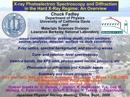
Chuck Fadley X-ray Photoelectron Spectroscopy and Diffraction in ...
Chuck Fadley X-ray Photoelectron Spectroscopy and Diffraction in ...
Chuck Fadley X-ray Photoelectron Spectroscopy and Diffraction in ...

You also want an ePaper? Increase the reach of your titles
YUMPU automatically turns print PDFs into web optimized ePapers that Google loves.
X-<strong>ray</strong> <strong>Photoelectron</strong> <strong>Spectroscopy</strong> <strong>and</strong> <strong>Diffraction</strong><br />
<strong>in</strong> the Hard X-Ray Regime: An Overview<br />
<strong>Chuck</strong> <strong>Fadley</strong><br />
Department of Physics<br />
University of California Davis<br />
<strong>and</strong><br />
Materials Sciences Division<br />
Lawrence Berkeley National Laboratory<br />
Basic considerations: prob<strong>in</strong>g depth, cross sections,<br />
source, analyzer, detector, surface vs. bulk sensitivity<br />
X-<strong>ray</strong> optics, spectral background, <strong>and</strong> st<strong>and</strong><strong>in</strong>g waves<br />
Core- <strong>and</strong> valence- level spectroscopy<br />
Valence b<strong>and</strong>s, the XPS limit, photon wave vector, phonons, etc.<br />
<strong>Photoelectron</strong> diffraction <strong>and</strong> Kikuchi b<strong>and</strong>s<br />
Summary <strong>and</strong> future prospects<br />
Plus see: Nucl. Inst. <strong>and</strong> Meth. A, Volume 547, Issue 1, Pages 1-238 (2005)<br />
2 nd Int’l Workshop-2006, Program/Abstrasts<br />
http://haxpes2006.spr<strong>in</strong>g8.or.jp/<br />
Special thanks to: C. Dallera, T. Hattori, K. Kobayashi, T. L. Lee, R.<br />
Moberg, G. Panaccione, O. Schaff, S. Suga, Y. Takata, J. Zegenhagen<br />
Japanese Physical Society Meet<strong>in</strong>g, Chiba, Sept., 2006
And 101 years later:<br />
Photoemission/photoelectron spectroscopy:<br />
UPS, XPS, ARPES<br />
<strong>Photoelectron</strong> diffraction:<br />
PD, XPD, PhD<br />
Typical photon energies: 5------------1500 eV<br />
laser, VUV soft x-<strong>ray</strong><br />
ΔE: ≤1 meV ∼50 meV<br />
Hard x-<strong>ray</strong> photoemission:<br />
HAXPES, HXPS, HIKE,…<br />
Photon energies from ∼5-15 keV?<br />
ΔE ∼50-75 meV→10 meV<br />
Why? To probe more bulklike properties, deeper <strong>in</strong>to multilayer structures,<br />
new physics, new applications…<br />
To date:<br />
• HAXPES2004 Workshop-ESRF (J. Zegenhagen)<br />
Nucl. Inst. <strong>and</strong> Meth. A, Volume 547, Issue 1, Pages 1-238 (2005)<br />
• HAXPES2006 Workshop-SPr<strong>in</strong>g8 (S. Suga, K. Kobayashi)<br />
Program/Abstracts @ http://haxpes2006.spr<strong>in</strong>g8.or.jp/<br />
• 20 published papers on “hard x-<strong>ray</strong> photoemission”, most from Japan<br />
• Talks by Tjeng, Suga, Sekiyama this morn<strong>in</strong>g,….
A first experiment<br />
SPEAR<br />
hν = 8,000 eV<br />
CMA, s<strong>in</strong>gle-channel det.<br />
25 cts./sec<br />
Siegbahn et al., late 1950s, then Pianetta, L<strong>in</strong>dau, Nature 250, 214 (1974)
Outl<strong>in</strong>e<br />
Basic considerations: prob<strong>in</strong>g depth, cross sections,<br />
source, analyzer, detector, surface vs. bulk sensitivity<br />
X-<strong>ray</strong> optics, spectral background<br />
St<strong>and</strong><strong>in</strong>g waves<br />
Core <strong>and</strong> valence spectroscopy<br />
Valence b<strong>and</strong>s, the XPS limit, photon wave vector, phonons, etc.<br />
<strong>Photoelectron</strong> diffraction <strong>and</strong> Kikuchi b<strong>and</strong>s<br />
Summary <strong>and</strong> future prospects
Electron <strong>in</strong>elastic mean free paths <strong>in</strong> solids—the “universal curve”<br />
Seah & Dench, Surf. Int. Anal. 1, 2 (1979)
Electron <strong>in</strong>elastic mean free paths <strong>in</strong> solids—the “universal curve”<br />
Graphite<br />
Germanium<br />
Tanuma, Powell, Penn, Surf. Interface Analysis, 17, 911-926 (1991);<br />
36, 1 (2004) <strong>and</strong> refs. there<strong>in</strong>
How much deeper do we<br />
probe at 5-10 keV?<br />
(nm)<br />
8<br />
7<br />
Typical elements:<br />
50-200 A<br />
• 6.93 nm<br />
Au<br />
Inelastic attenuation length<br />
TPP-2M formula<br />
of Tanuma, Powell, Penn<br />
6<br />
5<br />
∝ (E k<strong>in</strong> ) 0.75<br />
• 4.72 nm<br />
• 5.86 nm<br />
• 3.48 nm<br />
4-5x deeper<br />
than normal<br />
XPS<br />
• 2.07 nm<br />
15-20x deeper<br />
than normal<br />
ARPES<br />
| | | | |<br />
4000 6000 8000 10,000<br />
http://www.ss.teen.setsunan.ac.jp/e-imfp.html
Detection of SiO 2 /Si Interface Through Thick Overlayer<br />
Si 1s<br />
<strong>Photoelectron</strong>s<br />
Hard X-<strong>ray</strong><br />
NiGe<br />
SiO 2<br />
Si sub.<br />
Θ<br />
7∼15 nm<br />
12 nm<br />
Intensity (arb. units)<br />
Si 1s<br />
Θ = 80º<br />
NiGe Layer<br />
Thickness<br />
7 nm<br />
12 nm<br />
15 nm<br />
hν = 7935 eV<br />
SiO 2<br />
Si<br />
1850 1846 1842 1838 1834<br />
B<strong>in</strong>d<strong>in</strong>g energy (eV)<br />
H. Kondo et al. (Nagoya Univ.) unpublished.
High-k Dielectric Layers-post-deposition thermal anneal<strong>in</strong>g (PDA)<br />
temperature dependence of LaOx(4 nm)/Si(100) <strong>in</strong>terfaces (room temp<br />
deposition, 10m<strong>in</strong> anneal<strong>in</strong>g <strong>in</strong> N 2 ambient at 300 C, 400 C,<strong>and</strong> 500 C)<br />
La silicate formation by anneal<strong>in</strong>g<br />
Formation of <strong>in</strong>terface transition layers<br />
La Silicate (Si-O-La) is already formed by room<br />
temperature deposition. Amount of the silicate<br />
rapidly <strong>in</strong>creases by anneal<strong>in</strong>g.<br />
Electronegativities χ Si (1.8) > χ La (1.2)<br />
H. Nohira, et al., ECS Transactions, Vol. 1 (2005) pp. 87-95.
E k<strong>in</strong> ≈ 500-1000 eV<br />
Inner potential<br />
f(θ scat )<br />
Vary<strong>in</strong>g surface sensitivity for lower<br />
electron takeoff angles<br />
•<br />
Simplest <strong>in</strong>terpretation:<br />
Average emission depth = Λ <strong>in</strong>elastic s<strong>in</strong>θ takeoff<br />
How valid?<br />
E.g.: A. Jablonski <strong>and</strong> C. J. Powell,<br />
J. Vac. Sci. Tech. A 21, 274 (2003):<br />
→ Mean Emission Depth (MED)<br />
more relevant than Λ <strong>in</strong>elastic<br />
θ takeoff<br />
>20-30°<br />
E k<strong>in</strong> ≈ 10,000 eV<br />
PD modulations<br />
weaker<br />
f(θ scat )<br />
•<br />
θ takeoff<br />
down<br />
to 5-10°<br />
Simpler analysis<br />
Cleaner bulk & surface dist<strong>in</strong>ction<br />
C. J. Powell, W. Werner et al., priv. comm.;<br />
C.S.F., Nucl. Inst. & Meth. A 547, 24 (2005)
Variable takeoff-angle Si 1s photoelectron spectra<br />
from NiGe(12-nm)/SiO 2 (12-nm)/Si(100)<br />
Si 1s<br />
Si 1s<br />
8 keV<br />
hν = 7935 eV<br />
Si-O<br />
Si-Si<br />
Hard X-<strong>ray</strong><br />
NiGe<br />
SiO 2<br />
Si sub.<br />
Θ<br />
7∼15 nm<br />
12 nm<br />
Intensity [a. u .]<br />
More bulk<br />
sensitive<br />
More <strong>in</strong>terface sensitive<br />
θ = 80º<br />
35º<br />
12º<br />
1848<br />
1844<br />
1840<br />
1836<br />
B<strong>in</strong>d<strong>in</strong>g energy [eV]<br />
T. Hattori et al., Int. J. High Speed Electronics 16 (2006) 353.
<strong>Photoelectron</strong> <strong>in</strong>tensities from a semi-<strong>in</strong>f<strong>in</strong>ite substrate--<br />
atom Q with subshell nlj (e.g. Au4f 7/2 )<br />
I(Qnlj) = (<strong>in</strong>cident flux) × (area of illum<strong>in</strong>ated sample seen by analyzer)<br />
(Qnlj differential cross section) × (solid angle accepted by analyzer) ×<br />
(density of atoms Q) × (photoelectron <strong>in</strong>elastic attenuation length) ×<br />
(overall detection efficiency)<br />
I(Qnlj) = I 0 (hν) × (dσ Qnlj (hν→E k<strong>in</strong> )/dΩ) ×ρ Q ×Λ e (E k<strong>in</strong> ≈ hν) × A 0 /s<strong>in</strong>θ <strong>in</strong>c × Ω 0 × D 0<br />
Sample brightness = B 0<br />
Energy-dep. analyzer prop.<br />
Given atom @ high energy--lower l subshells favored (n- l -1 radial nodes) :<br />
dσ Qnlj (hν)/dΩ ∝1/(hν) N ≈1/(E k<strong>in</strong> ) N → For Au: 1/(E k<strong>in</strong> ) ∼2.0 for s subshells<br />
1/(E k<strong>in</strong> ) ∼2.5 for p subshells<br />
1/(E k<strong>in</strong> ) ∼3.0-3.5 for d subshells<br />
1/(E k<strong>in</strong> ) ∼4.0-4.5 for f subshell<br />
<strong>and</strong> Λ e (hν→E k<strong>in</strong> ) ∝ (E k<strong>in</strong> ) 0.75<br />
So <strong>in</strong>tensity per <strong>in</strong>cident photon falls off as 1/(E k<strong>in</strong> ) ∼1.25-3.75 !<br />
What can you do with the source, the analyzer+detector<br />
S.T. Manson<br />
10 11 -10 12 /s <strong>in</strong>to A 0 /s<strong>in</strong>θ <strong>in</strong>c<br />
a small spot<br />
C.J. Powell
Photon energy dependence of cross sections for gold<br />
Subshell Cross Section (Barns)<br />
1000000<br />
100000<br />
10000<br />
1000<br />
100<br />
10<br />
5p 3/2<br />
5d<br />
4f<br />
Au cross sections--Scofield<br />
5s,5p 1/2<br />
6s<br />
5s,p<br />
5d<br />
4f<br />
4s 1/2<br />
4p 1/2<br />
4p 3/2<br />
4d 3/2<br />
4d 5/2<br />
4f 5/2<br />
4f 7/2<br />
5s 1/2<br />
5p 1/2<br />
5p 3/2<br />
5d 3/2<br />
5d 5/2<br />
6s 1/2<br />
1<br />
0 2000 4000 6000 8000 10000 12000 14000 16000<br />
Photon Energy (eV)
Changes <strong>in</strong> relative cross<br />
section with photon energy<br />
Kunz et al., Nucl. Inst. & Meth. A 547, 73 (2005)
<strong>Photoelectron</strong> <strong>in</strong>tensities from a semi-<strong>in</strong>f<strong>in</strong>ite substrate--<br />
atom Q with subshell nlj (e.g. Au4f 7/2 )<br />
I(Qnlj) = (<strong>in</strong>cident flux) × (area of illum<strong>in</strong>ated sample seen by analyzer)<br />
(Qnlj differential cross section) × (solid angle accepted by analyzer) ×<br />
(density of atoms Q) × (photoelectron <strong>in</strong>elastic attenuation length) ×<br />
(overall detection efficiency)<br />
I(Qnlj) = I 0 (hν) × (dσ Qnlj (hν→E k<strong>in</strong> )/dΩ) ×ρ Q ×Λ e (E k<strong>in</strong> ≈ hν) × A 0 /s<strong>in</strong>θ <strong>in</strong>c × Ω 0 × D 0<br />
Sample brightness = B 0<br />
Energy-dep. analyzer prop.<br />
Given atom @ high energy--lower l subshells favored (n- l -1 radial nodes) :<br />
dσ Qnlj (hν)/dΩ ∝1/(hν) N ≈1/(E k<strong>in</strong> ) N → For Au: 1/(E k<strong>in</strong> ) ∼2.0 for s subshells<br />
1/(E k<strong>in</strong> ) ∼2.5 for p subshells<br />
1/(E k<strong>in</strong> ) ∼3.0-3.5 for d subshells<br />
1/(E k<strong>in</strong> ) ∼4.0-4.5 for f subshell<br />
<strong>and</strong> Λ e (hν→E k<strong>in</strong> ) ∝ (E k<strong>in</strong> ) 0.75<br />
So <strong>in</strong>tensity per <strong>in</strong>cident photon falls off as 1/(E k<strong>in</strong> ) ∼1.25-3.75 !<br />
What can you do with the source, the analyzer+detector<br />
S.T. Manson<br />
10 11 -10 12 /s <strong>in</strong>to A 0 /s<strong>in</strong>θ <strong>in</strong>c<br />
a small spot<br />
C.J. Powell
One experimental setup: SPr<strong>in</strong>g-8 8 BL29XU<br />
Y. Takata et al., Nuclear Instrum. <strong>and</strong> Methods A547, 50 (2005).<br />
T. Ishikawa et al., Nuclear Instrum. <strong>and</strong> Methods A547, 42 (2005).<br />
★ Excitation energy: 5.95 or 7.94keV, Δ(hν): 40-60meV<br />
★ Photon flux: 10 11 photons/sec @ 55(Hor.)x 50(Vert.) μm 2<br />
★ Analyzer: R4000-10kV (Gammadata-Scienta)<br />
Other mfrs.: MBS <strong>and</strong> Specs; Another project: Suga et al., ∼6x more flux
High Energy Resolution & High Throughput<br />
Au VB @ hν=5.95 keV<br />
ΔE=75<br />
meV<br />
at 5.95keV<br />
(E/ΔE=79000)<br />
ΔE=90meV<br />
at 7.94keV<br />
(E/ΔE=88000)<br />
E pass<br />
= 200eV<br />
220sec<br />
ΔE=208 meV<br />
E pass<br />
= 200eV<br />
30sec<br />
E pass<br />
=50eV<br />
335 meV<br />
Lorentzian<br />
Y. Takata et al., Nuclear Instrum. <strong>and</strong> Methods. A547, 50 (2005)
HAXPES/HXPS <strong>in</strong> the World<br />
• •<br />
•<br />
•<br />
•<br />
ESRF—Castro et al.<br />
Panaccione et al.<br />
Zegenhagen et al.<br />
Hasylab—Drube et al.<br />
BESSY---Bressler,Svensson et al.<br />
Felser, Fecher et al.<br />
SPr<strong>in</strong>g8—Kobayashi et al.<br />
Takata et al.<br />
Suga et al.<br />
???
<strong>Photoelectron</strong> <strong>in</strong>tensities from a semi-<strong>in</strong>f<strong>in</strong>ite substrate--<br />
atom Q with subshell nlj (e.g. Au4f 7/2 )<br />
I(Qnlj) = (<strong>in</strong>cident flux) × (area of illum<strong>in</strong>ated sample seen by analyzer)<br />
(Qnlj differential cross section) × (solid angle accepted by analyzer) ×<br />
(density of atoms Q) × (photoelectron <strong>in</strong>elastic attenuation length) ×<br />
(overall detection efficiency)<br />
I(Qnlj) = I 0 (hν) × (dσ Qnlj (hν→E k<strong>in</strong> )/dΩ) ×ρ Q ×Λ e (E k<strong>in</strong> ≈ hν) × A 0 /s<strong>in</strong>θ <strong>in</strong>c × Ω 0 × D 0<br />
Sample brightness = B 0<br />
Energy-dep. analyzer prop.<br />
Given atom @ high energy--lower l subshells favored (n- l -1 radial nodes) :<br />
dσ Qnlj (hν)/dΩ ∝1/(hν) N ≈1/(E k<strong>in</strong> ) N → For Au: 1/(E k<strong>in</strong> ) ∼2.0 for s subshells<br />
1/(E k<strong>in</strong> ) ∼2.5 for p subshells<br />
1/(E k<strong>in</strong> ) ∼3.0-3.5 for d subshells<br />
1/(E k<strong>in</strong> ) ∼4.0-4.5 for f subshell<br />
<strong>and</strong> Λ e (hν→E k<strong>in</strong> ) ∝ (E k<strong>in</strong> ) 0.75<br />
So <strong>in</strong>tensity per <strong>in</strong>cident photon falls off as 1/(E k<strong>in</strong> ) ∼1.25-3.75 !<br />
What can you do with the source, the analyzer+detector<br />
S.T. Manson<br />
10 11 -10 12 /s <strong>in</strong>to A 0 /s<strong>in</strong>θ <strong>in</strong>c<br />
a small spot<br />
C.J. Powell
Measurement of <strong>in</strong>elastic<br />
attenuation lengths<br />
º<br />
∝<br />
º<br />
º<br />
∝ E<br />
0.75 #<br />
k<strong>in</strong><br />
º<br />
∝ 0.75E<br />
0.50<br />
k<strong>in</strong><br />
#<br />
More accurate<br />
Dallara et al. NIMA 547, 113 (2005)
<strong>Photoelectron</strong> <strong>in</strong>tensities from a semi-<strong>in</strong>f<strong>in</strong>ite substrate--<br />
atom Q with subshell nlj (e.g. Au4f 7/2 )<br />
I(Qnlj) = (<strong>in</strong>cident flux) × (area of illum<strong>in</strong>ated sample seen by analyzer)<br />
(Qnlj differential cross section) × (solid angle accepted by analyzer) ×<br />
(density of atoms Q) × (photoelectron <strong>in</strong>elastic attenuation length) ×<br />
(overall detection efficiency)<br />
I(Qnlj) = I 0 (hν) × (dσ Qnlj (hν→E k<strong>in</strong> )/dΩ) ×ρ Q ×Λ e (E k<strong>in</strong> ≈ hν) × A 0 /s<strong>in</strong>θ <strong>in</strong>c × Ω 0 × D 0<br />
Sample brightness = B 0<br />
Energy-dep. analyzer prop.<br />
Given atom @ high energy--lower l subshells favored (n- l -1 radial nodes) :<br />
dσ Qnlj (hν)/dΩ ∝1/(hν) N ≈1/(E k<strong>in</strong> ) N → For Au: 1/(E k<strong>in</strong> ) ∼2.0 for s subshells<br />
1/(E k<strong>in</strong> ) ∼2.5 for p subshells<br />
1/(E k<strong>in</strong> ) ∼3.0-3.5 for d subshells<br />
1/(E k<strong>in</strong> ) ∼4.0-4.5 for f subshell<br />
<strong>and</strong> Λ e (hν→E k<strong>in</strong> ) ∝ (E k<strong>in</strong> ) 0.75<br />
So <strong>in</strong>tensity per <strong>in</strong>cident photon falls off as 1/(E k<strong>in</strong> ) ∼1.25-3.75 !<br />
What can you do with the source, the analyzer+detector<br />
S.T. Manson<br />
10 11 -10 12 /s <strong>in</strong>to A 0 /s<strong>in</strong>θ <strong>in</strong>c<br />
a small spot<br />
C.J. Powell
Quantitative analysis of peak <strong>in</strong>tensities us<strong>in</strong>g theoretical cross sections:<br />
La 0.7<br />
Sr 0.3<br />
MnO 3<br />
, hν = 7700 eV<br />
La4s<br />
Sr3s<br />
La4p: classis many-e - effect<br />
4p 5 4d n + configs. 4p 6 4d n-1 E<br />
1<br />
F<br />
Intensity (arb.units)<br />
5000<br />
Sr3p 1/2<br />
Sr3p 3/2<br />
La 4d<br />
La5s<br />
Sr4s<br />
Sr3d<br />
O2s,Sr4p,La5p<br />
Mn3s<br />
0<br />
Mn3p<br />
VB<br />
400 200 0<br />
B<strong>in</strong>d<strong>in</strong>g Energy (eV)<br />
Pard<strong>in</strong>i, Offi,<br />
Panaccione, CF, TBP
Quantitative analysis of peak <strong>in</strong>tensities us<strong>in</strong>g theoretical cross<br />
sections (Scofield): La 0.7 Sr 0.3 MnO 3 , hν = 7700 eV<br />
Concentration-weighted subshell cross sestion (Mb)<br />
1200<br />
1000<br />
800<br />
600<br />
400<br />
200<br />
0<br />
450<br />
400<br />
350<br />
300<br />
250<br />
200<br />
Mn3p<br />
150<br />
La5s<br />
Mn3s<br />
La4d<br />
Sr3s<br />
100<br />
50<br />
Sr4s Sr3d<br />
0<br />
0 5000 10000 15000 20000 25000<br />
La4p<br />
Core-level cross sections work very well→<br />
More accurate “bulk” quantitative analysis<br />
0 10000 20000 30000 40000 50000 60000 70000<br />
Core peak <strong>in</strong>tensity (a.u.)<br />
Pard<strong>in</strong>i, Offi,<br />
Panaccione, CF, TBP
Other considerations as energy <strong>in</strong>creases:<br />
--Atom recoil <strong>in</strong> core-level emission (ala Mőssbauer):<br />
•<br />
M<br />
1/2<br />
2 2<br />
⎛me<br />
⎞<br />
⎡E ⎛<br />
k<strong>in</strong><br />
2E ⎞<br />
k<strong>in</strong><br />
hν<br />
⎤ h ke<br />
-4 ⎡ E<br />
k<strong>in</strong>(eV)<br />
⎤<br />
E<br />
recoil<br />
(eV ) = hν<br />
⎜ 5.5 x 10<br />
2 2<br />
M<br />
⎟ ⎢ + ⎜ ⎟ + ⎥ ≈ ≈<br />
hν<br />
mc<br />
e<br />
2mc<br />
e<br />
2M<br />
⎢<br />
M(amu)<br />
⎥<br />
⎝ ⎠⎢ ⎣ ⎝ ⎠<br />
⎥⎦<br />
⎣ ⎦<br />
Fraction of transitions recoil free = f RF<br />
= exp(-3E recoil<br />
/2k B<br />
Θ D<br />
) at T = 0<br />
At 10 keV:<br />
= exp[-1.7x10 4 E recoil<br />
(eV)/Θ D<br />
(K)]<br />
Atom H C Ni Au<br />
E recoil<br />
6.0 eV 0.5 eV 0.1eV 0.03 eV<br />
Θ D<br />
(K) --- 2230 450 225<br />
f RF<br />
--- 0.02 0.02 0.10<br />
An extra energy shift/broaden<strong>in</strong>g? Yes-Takata et al., graphite!<br />
Source for electronic excitations?<br />
--Smear<strong>in</strong>g of coherent emission from valence b<strong>and</strong>s:<br />
Fraction of transitions that are “direct” with no phonon momentum k r phonon<br />
<strong>in</strong>volved: 1 st estimate ≈ Debye-Waller Factor = W(T) ≈ exp(-k<br />
2<br />
e<br />
)<br />
= exp(-CE k<strong>in</strong><br />
) (more later)
Experimental observation<br />
of atomic recoil <strong>in</strong> graphite:<br />
Theory us<strong>in</strong>g Debye model<br />
Takata et al.,<br />
arXiv:cond-mat/0609241 (11 Sep 2006)
Other considerations as energy <strong>in</strong>creases:<br />
--Atom recoil <strong>in</strong> core-level emission (ala Mőssbauer):<br />
•<br />
M<br />
1/2<br />
2 2<br />
⎛me<br />
⎞<br />
⎡E ⎛<br />
k<strong>in</strong><br />
2E ⎞<br />
k<strong>in</strong><br />
hν<br />
⎤ h ke<br />
-4 ⎡ E<br />
k<strong>in</strong>(eV)<br />
⎤<br />
E<br />
recoil<br />
(eV ) = hν<br />
⎜ 5.5 x 10<br />
2 2<br />
M<br />
⎟ ⎢ + ⎜ ⎟ + ⎥ ≈ ≈<br />
hν<br />
mc<br />
e<br />
2mc<br />
e<br />
2M<br />
⎢<br />
M(amu)<br />
⎥<br />
⎝ ⎠⎢ ⎣ ⎝ ⎠<br />
⎥⎦<br />
⎣ ⎦<br />
Fraction of transitions recoil free = f RF<br />
= exp(-3E recoil<br />
/2k B<br />
Θ D<br />
) at T = 0<br />
At 10 keV:<br />
= exp[-1.7x10 4 E recoil<br />
(eV)/Θ D<br />
(K)]<br />
Atom H C Ni Au<br />
E recoil<br />
6.0 eV 0.5 eV 0.1eV 0.03 eV<br />
Θ D<br />
(K) --- 2230 450 225<br />
f RF<br />
--- 0.02 0.02 0.10<br />
An extra energy shift/broaden<strong>in</strong>g? Yes-Takata et al., graphite!<br />
Source for electronic excitations?<br />
--Smear<strong>in</strong>g of coherent emission from valence b<strong>and</strong>s:<br />
Fraction of transitions that are “direct” with no phonon momentum k r phonon<br />
<strong>in</strong>volved: 1 st estimate ≈ Debye-Waller Factor = W(T) ≈ exp(-k<br />
2<br />
e<br />
)<br />
= exp(-C 1<br />
E k<strong>in</strong><br />
) exp(-C 2<br />
E k<strong>in</strong><br />
T) (more later)<br />
⎯⎯⎯→
Other considerations as energy <strong>in</strong>creases (cont’d) :<br />
Dipole<br />
--Non-dipole effects <strong>in</strong> matrix elements:<br />
r r r<br />
r r r<br />
r<br />
Int. ∝ Ψ | exp( ik • ) eˆ •∇| Ψ ≈ Ψ | (1 + ik • + ...) eˆ •∇| Ψ ≈ Ψ | eˆ<br />
•∇|<br />
Ψ<br />
f<br />
2 2 2<br />
hv i<br />
f hv<br />
i<br />
f<br />
• Photon momentum k r hv cannot always be neglected, e.g. <strong>in</strong><br />
r r r r r r r 2<br />
valence-b<strong>and</strong> studies: Int. ∝ u ˆ<br />
f<br />
exp( ikf • ) | exp( ikhv<br />
• r ) e • ∇ | uiexp( iki<br />
•<br />
)<br />
r r r r<br />
→ k + k + g = k<br />
• Additional non-dipole matrix elements: E2, M1,…<br />
i<br />
hv<br />
f<br />
i<br />
• And differential cross section more complex:<br />
φ<br />
θ p<br />
e - ê<br />
=<br />
light polarization<br />
dσ σ ⎡ β<br />
2 2<br />
⎤<br />
= 1 (3cos θ<br />
p<br />
1) ( δ γ cos θp )s<strong>in</strong>θpcosφ<br />
dΩ<br />
4π<br />
⎢<br />
+ − + +<br />
⎣ 2<br />
⎥<br />
⎦<br />
Dipole<br />
Non-Dipole<br />
≈ 1.0 at 4 keV electron energy<br />
Woodruff, Nucl. Inst. <strong>and</strong> Meth. A 547, 187 (2005)<br />
ˆk<br />
h ν
Outl<strong>in</strong>e<br />
Basic considerations: prob<strong>in</strong>g depth, cross sections,<br />
source, analyzer, detector, surface vs. bulk sensitivity<br />
X-<strong>ray</strong> optics, spectral background<br />
St<strong>and</strong><strong>in</strong>g waves<br />
Core <strong>and</strong> valence spectroscopy<br />
Valence b<strong>and</strong>s, the XPS limit, photon wave vector, phonons, etc.<br />
<strong>Photoelectron</strong> diffraction <strong>and</strong> Kikuchi b<strong>and</strong>s<br />
Summary <strong>and</strong> future prospects
Au 4f <strong>in</strong>tensity (counts/sec)→<br />
X-<strong>ray</strong> Optical Effects<br />
<strong>in</strong> Photoemission:<br />
The Beg<strong>in</strong>n<strong>in</strong>g<br />
B.L. Henke, Phys. Rev. A 6, 94 (1972)<br />
•Enhanced x-<strong>ray</strong> penetration depth as<br />
critical angle approached<br />
•Effects on average depth <strong>and</strong> <strong>in</strong>tensity<br />
<strong>in</strong> photoemission<br />
•Determ<strong>in</strong>ation of optical constants<br />
from data<br />
θ c<br />
<strong>in</strong>c<br />
θ <strong>in</strong>c<br />
e -<br />
Incidence angle (degrees)→<br />
X-<strong>ray</strong> attenuation length (Å)→<br />
Au 4f <strong>in</strong>tensity (normalized)→<br />
1487 eV 183 eV 109 eV<br />
Incid. angle (mrad)→<br />
Critical angle (mrad)→<br />
θ crit<br />
X-<strong>ray</strong> optical theory<br />
Experiment<br />
Incidence angle (mrad)→
Problem: <strong>in</strong>elastic<br />
backgrounds <strong>in</strong> core<br />
spectra with multi-keV<br />
excitation-<br />
Solution: reduction via<br />
total reflection<br />
Kawai et al., Spectrochim.<br />
Acta B 47, 983 (‘92)<br />
Chester & Jach, Phys. Rev.<br />
B 4817262 (’93)<br />
Jach & L<strong>and</strong>ree, Surf. & Int.<br />
Anal. 31, 768 (‘01)<br />
The JEOL JPS-9010MC<br />
e -<br />
lens
Surface Insensitivity & High Throughput<br />
<strong>in</strong>c<br />
<strong>Photoelectron</strong> Intensity<br />
SiO 2<br />
-0.8nm/Si(100)<br />
hν=7.94 keV<br />
θ=1 deg.<br />
30 sec!!<br />
Si 2p<br />
SiO 2<br />
Si<br />
7830 7835 7840<br />
K<strong>in</strong>etic Energy (eV)<br />
Takata et al., SPr<strong>in</strong>g8
Outl<strong>in</strong>e<br />
Basic considerations: prob<strong>in</strong>g depth, cross sections,<br />
source, analyzer, detector, surface vs. bulk sensitivity<br />
X-<strong>ray</strong> optics, spectral background<br />
St<strong>and</strong><strong>in</strong>g waves<br />
Core <strong>and</strong> valence spectroscopy<br />
Valence b<strong>and</strong>s, the XPS limit, photon wave vector, phonons, etc.<br />
<strong>Photoelectron</strong> diffraction <strong>and</strong> Kikuchi b<strong>and</strong>s<br />
Summary <strong>and</strong> future prospects
St<strong>and</strong><strong>in</strong>g wave formation <strong>in</strong> reflection from a surface,<br />
or s<strong>in</strong>gle-crystal Bragg planes + , or a multilayer mirror<br />
Incident<br />
Reflected<br />
1<br />
e - hν<br />
λ SW (|E 2 |) =<br />
λ x /2s<strong>in</strong>θ <strong>in</strong>c<br />
R<br />
• Rock<strong>in</strong>g curve:<br />
I(θ ) ∝ 1 + R(θ ) + 2 R(θ ) f cos[φ(θ ) −<br />
2πP]<br />
<strong>in</strong>c <strong>in</strong>c <strong>in</strong>c <strong>in</strong>c<br />
• Energy scan:<br />
I(hν ) ∝ 1 + R( hν ) + 2 R( hν ) f cos[φ( hν ) −<br />
2πP]<br />
with: f = coherent fraction, P = phase of atomic position<br />
% modulation ≈<br />
100 x 4√R<br />
∴ R = 5% → 90% mod.<br />
• Phase scan with wedge-shaped sample (“Swedge” method):<br />
+<br />
St<strong>and</strong><strong>in</strong>g waves via Bragg reflection of hard x-<strong>ray</strong>s: Batterman, Phys. Rev A 133, 759 (1964)
St<strong>and</strong><strong>in</strong>g waves <strong>in</strong> Bragg reflection from TiO 2 :<br />
Scann<strong>in</strong>g energy with<strong>in</strong> Bragg rock<strong>in</strong>g curve--hν = 3 keV<br />
St<strong>and</strong><strong>in</strong>g<br />
wave on Ti<br />
St<strong>and</strong><strong>in</strong>g<br />
wave on O<br />
Woicik, NIMA 547, 227 (2005)<br />
<strong>and</strong> earlier papers
0.009400<br />
0.008080<br />
0.006760<br />
0.005440<br />
0.004120<br />
0.002800<br />
Site-specific valence electronic structure of SrTiO3<br />
S. Thieß, T.-L. Lee, F. Bott<strong>in</strong>, B. Cowie <strong>and</strong> J. Zegenhagen<br />
Relative photon energy ΔE (eV)<br />
normalised Intensities<br />
Intensity [a.u.]<br />
0.6<br />
0.4<br />
0.2<br />
0.0<br />
B<strong>in</strong>d<strong>in</strong>g energy (eV)<br />
10 9 8 7 6 5 4 3<br />
E = 2.75 keV<br />
Ti<br />
Sr<br />
SrTiO 3<br />
valence b<strong>and</strong><br />
O 3<br />
ΔE<br />
+<br />
+<br />
10 9 8 7 6 5 4 3<br />
B<strong>in</strong>d<strong>in</strong>g energy (eV)<br />
Valence b<strong>and</strong> XSW<br />
_-<br />
-<br />
Ti<br />
2p<br />
+ 0.5<br />
Sr<br />
O<br />
Ti<br />
(111)<br />
Reflectivity<br />
0.8 0.6 0.4 0.2 0.0<br />
SrTiO 3<br />
(111)<br />
O<br />
Sr<br />
1s<br />
3p<br />
2.0 1.5 1.0 0.5 0.0<br />
normalised Intensity<br />
Core-level XSW<br />
0.6<br />
0.4<br />
0.2<br />
0.0<br />
Relative photon energy ΔE (eV)<br />
(112)
Prob<strong>in</strong>g Buried Interfaces<br />
with Soft X-<strong>ray</strong> St<strong>and</strong><strong>in</strong>g<br />
Wave/Wedge (“Swedge”)<br />
Method: core spectra<br />
<strong>and</strong> depth distributions<br />
X-<strong>ray</strong><br />
900 eV<br />
<strong>Photoelectron</strong><br />
Al 2 O 3 /Co 65 Pt 35 /Ru cap:<br />
Tunnel junction system<br />
(see Kaiser et al., PRL<br />
94, 247203 (2005)<br />
12Å Ru cap with Oxide surface<br />
15Å CoPt(65/35)<br />
30 sec oxidation<br />
Al 2 O 3 wedge<br />
θ Bragg<br />
Scanned st<strong>and</strong><strong>in</strong>g wave<br />
∼0.1 mm<br />
spot<br />
M Co<br />
Multilayer<br />
Mirror<br />
B 4 C<br />
W<br />
B 4 C<br />
W<br />
Sell, Yang, Watanabe,<br />
Mun, Park<strong>in</strong> et al., TBP<br />
SiO 2<br />
Si-wafer<br />
Scanned sample<br />
∼6.0 mm
Representative spectra:<br />
4100000<br />
4000000<br />
3900000<br />
3800000<br />
3700000<br />
3600000<br />
3500000<br />
3400000<br />
Co 2p<br />
Co<br />
500000<br />
450000<br />
400000<br />
350000<br />
300000<br />
Co 2+<br />
250000<br />
200000<br />
150000<br />
Pt 4f<br />
2200000<br />
2000000<br />
Ru 3d<br />
1800000<br />
1600000<br />
1400000<br />
1200000<br />
1000000<br />
800000<br />
600000<br />
400000<br />
200000<br />
0<br />
300 295 290 285 280 275 270 265<br />
B<strong>in</strong>d<strong>in</strong>g Energy (eV)<br />
784 782 780 778 776 774 772 770<br />
B<strong>in</strong>d<strong>in</strong>g Energy (eV)<br />
100000<br />
50000<br />
84 82 80 78 76 74 72 70 68 66 64 62 60<br />
Intensity (arb. unit)<br />
O 1s<br />
Adsorbed<br />
O<br />
RuO x<br />
B<strong>in</strong>d<strong>in</strong>g Energy (eV)<br />
B.C. Sell et al.<br />
40000<br />
35000<br />
30000<br />
25000<br />
20000<br />
15000<br />
10000<br />
VB<br />
5000<br />
536 534 532 530 528 526 524 522<br />
B<strong>in</strong>d<strong>in</strong>g Energy (eV)<br />
0<br />
12 10 8 6 4 2 0 -2 -4 -6<br />
B<strong>in</strong>d<strong>in</strong>g Energy (eV)
Co 2p spectrum dur<strong>in</strong>g a st<strong>and</strong><strong>in</strong>g wave scan<br />
2.4 eV<br />
7.0 eV<br />
Kl<strong>in</strong>genberg et al., Surf.<br />
Sci. 283, 13 (1997)
St<strong>and</strong><strong>in</strong>g waves from multilayers <strong>in</strong> the hard x-<strong>ray</strong> regime<br />
Electric Field Strength (|E| 2 )<br />
Reflectivity<br />
0.0 0.5 1.0<br />
(a)<br />
(c)<br />
R = 0.28<br />
hν = 1.0 keV<br />
0.0 5.0 10.0 15.0<br />
Incidence angle (°)<br />
2.5 Vac. B 4<br />
C/W Multilayer<br />
2.0<br />
1.5<br />
1.0<br />
0.5<br />
0.0<br />
-100 0 100 200 300 400 500<br />
Depth, z (Å)<br />
1.0 keV<br />
θ Bragg<br />
= 9.3 o<br />
Reflectivity<br />
0.0 0.5 1.0<br />
(b)<br />
(d)<br />
Electric Field Strength (|E| 2 )<br />
R = 0.80<br />
hν = 10.0 keV<br />
0.0 1.0 2.0 3.0<br />
Incidence angle (°)<br />
4.0 Vac. B 4<br />
C/W Multilayer<br />
3.5<br />
3.0<br />
2.5<br />
2.0<br />
1.5<br />
1.0<br />
0.5<br />
10.0 keV<br />
θ Bragg<br />
= 0.93 o<br />
0.0<br />
-100 0 100 200 300 400 500<br />
Depth, z (Å)<br />
S.H. Yang
Outl<strong>in</strong>e<br />
Basic considerations: prob<strong>in</strong>g depth, cross sections,<br />
source, analyzer, detector, surface vs. bulk sensitivity<br />
X-<strong>ray</strong> optics, spectral background<br />
St<strong>and</strong><strong>in</strong>g waves<br />
Core <strong>and</strong> valence spectroscopy<br />
Valence b<strong>and</strong>s, the XPS limit, photon wave vector, phonons, etc.<br />
<strong>Photoelectron</strong> diffraction <strong>and</strong> Kikuchi b<strong>and</strong>s<br />
Summary <strong>and</strong> future prospects
LaMnO 3 th<strong>in</strong> film--2p core levels<br />
with vary<strong>in</strong>g degrees of surface sensitivity<br />
“Surface”<br />
“Near-Surface”<br />
“Bulk”<br />
Bulkassociated<br />
screen<strong>in</strong>g<br />
feature<br />
Horiba et al., PRL 93, 236401 (2004)
Electronic Structure of Stra<strong>in</strong>ed Manganite Th<strong>in</strong> Films with Room Temperature<br />
Ferromagnetism Investigated by Hard X-<strong>ray</strong> Photoemission <strong>Spectroscopy</strong>:<br />
La 0.85<br />
Ba 0.15<br />
MnO 3<br />
5.95 keV<br />
Stra<strong>in</strong>/Mag<br />
netismassociated<br />
screen<strong>in</strong>g<br />
feature<br />
Tanaka et al., Spr<strong>in</strong>g8, PRB, <strong>in</strong> press
Fractured “cubic” La 0.7<br />
Sr 0.3<br />
MnO 3<br />
T = 150K<br />
Manella et al., TBP<br />
Pard<strong>in</strong>i, Offi, Panaccione, CF, TBP
Electronic Structure of Bulk Manganite Crystals with No Room Temperature<br />
Remanent FM Investigated by Hard X-<strong>ray</strong> Photoemission <strong>Spectroscopy</strong>:<br />
“Cubic” La 0.7<br />
Sr 0.3<br />
MnO 3<br />
—fractured <strong>in</strong> situ<br />
Intensity (arb.units)<br />
30000<br />
25000<br />
hν = 7700 eV<br />
∼ 0.5 eV<br />
Opposite<br />
Direction<br />
∼ No shift<br />
T<br />
150<br />
300<br />
423<br />
T C<br />
Structural<br />
<strong>and</strong>/or<br />
SRMOassociated<br />
screen<strong>in</strong>g<br />
feature?<br />
20000<br />
665 660 655 650 645 640 635<br />
B<strong>in</strong>d<strong>in</strong>g energy (eV)<br />
Pard<strong>in</strong>i, Offi, Panaccione, CF, TBP
Temperature-<br />
Dependent<br />
Soft X-Ray<br />
Photoemission :<br />
La 0.7<br />
Sr 0.3<br />
MnO 3<br />
(a)<br />
O more positive<br />
Mn higher sp<strong>in</strong>,<br />
more negative<br />
Mannella et al.,<br />
Phys. Rev. Lett. 92,<br />
166401 (2004)<br />
<strong>Photoelectron</strong> Intensity (a.u.)<br />
(c)<br />
BE Displacement (meV)<br />
1000<br />
800<br />
600<br />
400<br />
200<br />
LSMO, x = 0.3, T dependence of Mn 3s<br />
T = 135 K<br />
T max = 500 K<br />
T C = 370 K<br />
T = 110 K<br />
0<br />
96<br />
94<br />
92<br />
90<br />
ΔE 3s<br />
88<br />
86<br />
84<br />
82<br />
B<strong>in</strong>d<strong>in</strong>g Energy (eV)<br />
Mn 3s<br />
hv = 212 eV<br />
Longer<br />
times<br />
Mn 3s<br />
hv = 212 eV<br />
80<br />
-200<br />
100 150 200 250 300 350 400 450 500 550<br />
Temperature (K)<br />
T<br />
I<br />
M<br />
E<br />
78<br />
T dependence of Mn 3s b<strong>in</strong>d<strong>in</strong>g energies<br />
(b)<br />
<strong>Photoelectron</strong> Intensity (a.u.)<br />
T c<br />
T sat Change <strong>in</strong> ΔE 3s<br />
Average 3s BE<br />
TIME→<br />
T sat<br />
(d)<br />
LSMO, x = 0.3, T dependence of O 1s<br />
T = 135 K<br />
T max = 500 K<br />
T C = 370 K<br />
T = 110 K<br />
533 532 531<br />
BE Displacement (meV)<br />
400<br />
300<br />
200<br />
100<br />
0<br />
“Bulk”<br />
“Surface”<br />
530 529 528<br />
B<strong>in</strong>d<strong>in</strong>g Energy (eV)<br />
O 1s-”bulk”<br />
hv = 652 eV<br />
O1s<br />
T c<br />
O 1s<br />
hv = 652 eV<br />
T<br />
I<br />
M<br />
E<br />
527 526 525<br />
T dependence of O 1s b<strong>in</strong>d<strong>in</strong>g energy<br />
TIME→<br />
-100<br />
100 150 200 250 300 350 400 450 500 550<br />
Temperature (K)<br />
T sat
e<br />
Stra<strong>in</strong>/Mag<br />
netismassociated<br />
screen<strong>in</strong>g<br />
feature<br />
Pard<strong>in</strong>i, Offi,<br />
Panaccione, CF, TBP<br />
T = 110 K (start)<br />
T = 500 K (T max<br />
)<br />
T = 110 K (start)<br />
T = 500 K<br />
Mannella et al.,<br />
Phys. Rev. Lett. 92,<br />
166401 (2004)<br />
Qualitat. the<br />
same, but<br />
still some<br />
surface<br />
<strong>in</strong>fluence?
More dramatic screen<strong>in</strong>g effects <strong>in</strong> strongly correlated materials—<br />
high T C Nd 2-x<br />
Ce x<br />
CuO 4<br />
(5.9keV)<br />
(1.5keV)<br />
M. Taguchi et al., Phys. Rev. Lett. 95, 17702 (2005).
(6.0 keV)<br />
(1.5 keV)<br />
Evidence for a suppressed core-hole<br />
screen<strong>in</strong>g on the surface of hightemperature<br />
superconductors<br />
La 2-x<br />
Sr x<br />
CuO 4<br />
<strong>and</strong> Nd 2-x<br />
Ce x<br />
CuO 4<br />
Intense screened/shakedown peak <strong>in</strong> e-<br />
doped cuprates<br />
Zhang-Rice s<strong>in</strong>glet <strong>in</strong> LCO not <strong>in</strong> NCCO<br />
Screen<strong>in</strong>g due to delocalized coherent<br />
state at E F<br />
Screen<strong>in</strong>g with<strong>in</strong> the first 15 Å of the<br />
surface is different from the bulk!<br />
M. Taguchi et al.,<br />
PRL 95, 177002 (2005)
V 2 O 3 --2p core level--transfer of spectral weight across<br />
the metal-<strong>in</strong>sulator transition<br />
Photoemission Intensity (Arb. Units)<br />
V 2p core level--hν = 5934 eV<br />
300 K (PM phase)<br />
140 K (AFI phase)<br />
Difference<br />
Photoemission Intensity (Arb. Units)<br />
T= 190 K<br />
T= 180 K<br />
T= 170 K<br />
T= 155 K<br />
T= 145 K<br />
hν = 5934 eV<br />
V 2p 3/2<br />
525 520 515 510<br />
B<strong>in</strong>d<strong>in</strong>g Energy (eV)<br />
518 516 514 512<br />
B<strong>in</strong>d<strong>in</strong>g Energy (eV)<br />
G. Panaccioned et al., VOLPE @ ESRF
Core <strong>and</strong> valence effects <strong>in</strong> V 2 O 3<br />
Photoemission Intensity (Arb. units)<br />
QP peak<br />
V 3d<br />
Sample 1 (flat)<br />
Sample 2 (rough)<br />
Polished<br />
Screen<strong>in</strong>g/<br />
Shakedown<br />
V 2p 3/2<br />
G. Panaccione et al., VOLPE ESRF<br />
2.5 2.0 1.5 1.0 0.5 0.0<br />
B<strong>in</strong>d<strong>in</strong>g Energy (eV)<br />
514 513 512<br />
B<strong>in</strong>d<strong>in</strong>g energy (eV)<br />
See also: M. Taguchi et al. PRB 71, 155102 (2005)
Valence effects <strong>in</strong> the metal-to-<strong>in</strong>sulator transition of VO 2<br />
Photoemission <strong>in</strong>tensity (arb. units)<br />
a<br />
12 8 4 0<br />
b<br />
O 2p<br />
valence<br />
b<strong>and</strong><br />
3 2 1 0 -1<br />
c<br />
1<br />
B<strong>in</strong>d<strong>in</strong>g energy (eV)<br />
Metal<br />
Insulator<br />
V 3d<br />
350 K<br />
PES data<br />
PES/FD<br />
0<br />
O 2p valence b<strong>and</strong> : clear change<br />
I: two peaks at 7.3 <strong>and</strong> 5.2 eV.<br />
7.3 eV peak shifts toward E F<br />
by<br />
0.6 eV. The high E B<br />
tail is<br />
enhanced around 9 eV.<br />
⇐<strong>in</strong>creased hybridization <strong>in</strong> the<br />
M phase. The threshold of the<br />
non bond<strong>in</strong>g peak between 5 <strong>and</strong><br />
2.7 eV shifts by 0.3 eV toward E F<br />
.<br />
3d peak is at 0.9 eV <strong>in</strong> I phase.<br />
M<strong>in</strong>imum gap is 0.28 eV. (π b<strong>and</strong> is<br />
expected ∼0.5 eV above E F<br />
.<br />
(Interb<strong>and</strong> gap can be 0.78 eV.)<br />
M phase: FD cut off. QP DOS<br />
<strong>in</strong>creases beyond E F<br />
. Higher<br />
energy tail of 3d spectra is due to<br />
the <strong>in</strong>coherent state. 0.9 eV peak<br />
<strong>in</strong> I phase is a coherent QP.<br />
Crystal distortion⇒b<strong>and</strong> changes<br />
⇒trigger MIT (renorm. Peierls Ins.)<br />
Suga et al.
Outl<strong>in</strong>e<br />
Basic considerations: prob<strong>in</strong>g depth, cross sections,<br />
source, analyzer, detector, surface vs. bulk sensitivity<br />
X-<strong>ray</strong> optics, spectral background<br />
St<strong>and</strong><strong>in</strong>g waves<br />
Core <strong>and</strong> valence spectroscopy<br />
Valence b<strong>and</strong>s, the XPS limit, photon wave vector, phonons, etc.<br />
<strong>Photoelectron</strong> diffraction <strong>and</strong> Kikuchi b<strong>and</strong>s<br />
Summary <strong>and</strong> future prospects
Valence-B<strong>and</strong> Photoemission at High Energy--<br />
What & Where is the “XPS Limit”?:<br />
Additional effects at higher energies:<br />
• non-dipole--the photon momentum<br />
• angular acceptance→B.Z. averag<strong>in</strong>g<br />
• lattice recoil, phonon creation→more<br />
k hν @<br />
1,253 eV<br />
k hν @<br />
10,000 eV<br />
B.Z. averag<strong>in</strong>g, ∼Debye-Waller factor = W(T) ≈ exp[-(k f ) 2 ]<br />
….the “XPS limit” of full B.Z. averag<strong>in</strong>g <strong>and</strong><br />
D.O.S. sensitivity<br />
Hussa<strong>in</strong> et al., Phys.<br />
Rev. B 22, 3750 (‘80)
XPS <strong>and</strong> HXPS <strong>in</strong> k space:<br />
hν = 1254 eV<br />
r r r r<br />
f<br />
ki<br />
+ g = k −kh<br />
ν<br />
hν = 10,000 eV<br />
r<br />
g = 26(2 π / a)yˆ<br />
f<br />
k r<br />
k f = 25.80 (2π/a), k hν<br />
= 2.54(2π/a)<br />
g r<br />
ACCEPTANCE<br />
CONE OF ±0.5°<br />
−k r<br />
h ν<br />
Angular resolutions<br />
of 0.02º with an acceptance<br />
±2º may be possible!<br />
B. Wannberg, P. Balzer
Gold Valence Spectrum<br />
In the XPS Limit<br />
Intensity (a.u.)<br />
XPS<br />
Broadened<br />
Theo. DOS<br />
10 8 6 4 2 0<br />
B<strong>in</strong>d<strong>in</strong>g energy (eV)<br />
E F<br />
15<br />
10<br />
Gold Valence Spectrum<br />
300 (b) K<br />
D.W.<br />
factor<br />
≈ 6x10 -6 !<br />
Siegbahn XPS @ 1.487 keV<br />
Silver Valence Spectrum<br />
5<br />
0<br />
Fixed mode<br />
Measurement Time 3:40 x1<br />
5938<br />
5940<br />
5942<br />
5944<br />
5946<br />
5948<br />
5950<br />
Intensity (a.u.)<br />
XPS<br />
Broadened<br />
Theo. DOS<br />
E F<br />
eV<br />
Measurement time: 3 m<strong>in</strong> 40 s<br />
Total resolution: ca. 80 meV<br />
Takata et al., SPr<strong>in</strong>g8 @ 5.495 keV<br />
10 8 6 4 2 0<br />
B<strong>in</strong>d<strong>in</strong>g energy (eV)
In the XPS<br />
Limit—<br />
Comparison to<br />
theoretical<br />
DOSs<br />
15<br />
10<br />
Total DOS<br />
Expt.<br />
(b)<br />
Takata et al.,<br />
SPr<strong>in</strong>g8 @<br />
5.495 keV<br />
5<br />
High energy<br />
suggests analysis as:<br />
B<strong>and</strong> / MO<br />
dσ<br />
dσ<br />
∝ |P |<br />
AO<br />
j 2 Aλ<br />
∑ Aλj<br />
dΩ Atom A dΩ<br />
Orbital λ<br />
with P<br />
Aλj<br />
=<br />
0<br />
5938<br />
projected density of states<br />
or MO population analysis<br />
Fixed mode<br />
Measurement Time 3:40 x1<br />
5940<br />
5942<br />
5944<br />
5946<br />
eV<br />
5948<br />
5950<br />
Cross sec.<br />
6s x 5 1.00<br />
6p x 5 -----<br />
5d total 3.88<br />
5d e g<br />
5d t 2g<br />
Z. Y<strong>in</strong><br />
W.E. Pickett<br />
E F
Normalized Intensity<br />
In the XPS Limit<br />
SiO 2 -0.58nm/Si(100)<br />
@0.85keV<br />
(Exp.)<br />
SiO 2<br />
@7.94keV<br />
(Exp.)<br />
a<br />
20 15 10 5 0<br />
b<br />
c<br />
B<strong>in</strong>d<strong>in</strong>g Energy (eV)<br />
XPS—<br />
850 eV<br />
HXPS—<br />
7940 eV<br />
300 sec!!<br />
Theory:<br />
Si DOS<br />
s<br />
p<br />
a b c<br />
σ Si3s<br />
(8 keV) = 14.9 Barns<br />
∼1/27<br />
σ Si3p<br />
(8 keV) = 0.54 Barns<br />
Takata et al.,<br />
Appl.Phys.Lett.<br />
84, 4310 (2004)<br />
Papaconstantopoulos
W at room temp.—not<br />
quite the XPS limit: Effect<br />
of photon momentum on k<br />
conservation: W(110) at<br />
1253.6 eV <strong>and</strong> room temp.<br />
W(001)<br />
300 K<br />
hν<br />
hν<br />
hν<br />
Symmetry-related<br />
spectra shifted by<br />
6.0° for best match.<br />
Calculated 4.8°<br />
due to k hν<br />
Hussa<strong>in</strong> et al.,<br />
Phys. Rev. 22,<br />
3750 (1980)
Suppression<br />
of direct-transition<br />
effects with<br />
temperature:<br />
W(110) at 1253.6 eV<br />
Hussa<strong>in</strong> et al.,<br />
Phys. Rev. 22,<br />
3750 (1980)
Alum<strong>in</strong>um soft x-<strong>ray</strong> valence spectra: Direct transitions to >710 eV<br />
Surface<br />
state<br />
300 K<br />
W = 0.19<br />
Surface—<br />
less affected?<br />
Hofmann et al., PRB 66, 245422 (2002)
T = 300K, T/Θ Debye<br />
= 0.75<br />
B<strong>in</strong>d<strong>in</strong>g energy (eV)<br />
12 10 8 6 4 2 0 -2<br />
B<strong>in</strong>d<strong>in</strong>g energy (eV)<br />
12 10 8 6 4 2 0 -2<br />
90 95 100 105<br />
Emission angle (deg)<br />
470K, 1.18 607K, 1.52 780K, 1.95<br />
90 95 100 105<br />
Emission angle (deg)<br />
90 95 100 105<br />
Emission angle (deg)<br />
90 95 100 105<br />
Emission angle (deg)<br />
780K<br />
607K<br />
470K<br />
300K<br />
12 10 8 6 4 2 0 2<br />
780K 780K, .22<br />
607K, .31<br />
470K 470K, .40<br />
300K, D.W. = 0.55<br />
W(110)<br />
T-Dep. Soft X-Ray<br />
ARPES<br />
hν = 260 eV<br />
90º = normal<br />
800 angle channels<br />
Θ Debye<br />
= 400K<br />
L. Pluc<strong>in</strong>ski<br />
B.C. Sell<br />
Absolute photocurrent-20 channels (a.u.)<br />
Absolute photocurrent-20 channels (a.u.)<br />
B<strong>in</strong>d<strong>in</strong>g energy (eV)<br />
12 10 8 6 4 2 0 -2<br />
B<strong>in</strong>d<strong>in</strong>g energy (eV)<br />
12 10 8 6 4 2 0 -2
The W B<strong>and</strong><br />
Structure<br />
(Christensen &<br />
Feuerbacher;<br />
Byl<strong>and</strong>er &<br />
Kle<strong>in</strong>man)<br />
“Gap”
W(110)<br />
Soft X-Ray ARPES<br />
Compared to simple DT theory<br />
hν = 260 eV<br />
90º = normal<br />
T = 300K<br />
Free-e - DT<br />
Theory<br />
“Gap”<br />
|<br />
Γ<br />
|<br />
N<br />
[110]<br />
L. Pluc<strong>in</strong>ski<br />
Free-e - DT<br />
Theory<br />
+ Secondary cones?
T = 300K, T/Θ 300K Debye<br />
= 0.75 470K, 1.18 607K, 1.52 780K, 780K 1.95<br />
“Gap”<br />
|<br />
N<br />
|<br />
Γ<br />
Absolute photocurrent-20 channels (a.u.)<br />
D.O.S.<br />
14 12 10 8 6 4 2 0<br />
780K, .22<br />
607K, .31<br />
470K, .40<br />
300K, D.W. = .55<br />
W(110)<br />
Not-So-Soft X-Ray ARPES<br />
hν = 870 eV<br />
90º = normal<br />
800 angle channels<br />
Θ Debye<br />
= 400K<br />
L. Pluc<strong>in</strong>ski
W(110) X-Ray ARPES<br />
Not-So-Soft X-Ray ARPES<br />
Compared to simple DT theory<br />
hν = 870 eV & 900 eV<br />
90º = normal<br />
T = 300K<br />
L. Pluc<strong>in</strong>ski<br />
|<br />
N<br />
870 eV<br />
|<br />
Γ<br />
870 eV 900 eV
Now take it up to 10 keV:<br />
hν = 870 eV<br />
T = 780K<br />
W ≈ 0.21<br />
hν = 10,000 eV<br />
r<br />
g = 26(2 π / a)yˆ<br />
f<br />
k r<br />
k f = 25.80 (2π/a), k hν<br />
= 2.54(2π/a)<br />
g r<br />
ACCEPTANCE<br />
CONE OF ±0.5°<br />
−k r<br />
h ν<br />
Θ Debye = 310K, (10 -20 cm 2 ) = 5.34 + 0.0583T 0.0583T<br />
Debye-Waller Factor = W(T) ≈ exp(-k e<br />
2<br />
)<br />
High T<br />
⎯⎯⎯→<br />
High T<br />
⎯⎯⎯→<br />
= exp(-C 1<br />
E k<strong>in</strong><br />
) exp(-C 2<br />
E k<strong>in</strong><br />
T)<br />
W at 4K: W ≈ 0.21, ≈ 21% direct<br />
at 77K: W ≈ 0.16, ≈ 16% direct<br />
at 300K: W ≈ 0.01, ≈ 1% direct<br />
Correlated vibrations <strong>and</strong> a better theory (e.g. Phys. Rev. B 35, 1147<br />
(‘87) <strong>and</strong> 53, 7524 (’96) + 54, 14703 (‘96)) may suggest higher DT<br />
percentages, but needs further E&T study
Quantitative systematics—Tungsten :<br />
Debye-Waller Factor =<br />
sensitive<br />
More than<br />
50% b<strong>and</strong>
Outl<strong>in</strong>e<br />
Basic considerations: prob<strong>in</strong>g depth, cross sections,<br />
source, analyzer, detector, surface vs. bulk sensitivity<br />
X-<strong>ray</strong> optics, spectral background<br />
St<strong>and</strong><strong>in</strong>g waves<br />
Core <strong>and</strong> valence spectroscopy<br />
Valence b<strong>and</strong>s, the XPS limit, photon wave vector, phonons, etc.<br />
<strong>Photoelectron</strong> diffraction <strong>and</strong> Kikuchi b<strong>and</strong>s<br />
Summary <strong>and</strong> future prospects
<strong>Photoelectron</strong><br />
diffraction→<br />
holography:<br />
Elementspecific<br />
short-range<br />
atomic<br />
structure<br />
FORWARD SCATT. = “O TH ORDER”<br />
θ scat<br />
HIGHER ORDERS<br />
Bond & Low-Index<br />
Directions<br />
Bond Lengths<br />
&<br />
Atomic<br />
Positions<br />
→Holographic<br />
fr<strong>in</strong>ges
<strong>Photoelectron</strong> diffraction: F<strong>in</strong>e structure at ∼1 keV energy<br />
φ = 0°<br />
[001]<br />
hν<br />
θ <strong>in</strong>c<br />
[011]<br />
φ<br />
W(011)<br />
e -<br />
θ<br />
AZIMUTHAL ANGLE φ
XPD @ 1 keV<br />
B 1s from hex-BN<br />
monolayer on<br />
Ni(111)<br />
N on-top on Ni(111)<br />
B fcc on Ni(111), 0.1 Å below N<br />
Expt.-Osterwalder et al<br />
Theory-Osterwalder et al.<br />
Program by Kaduwela
X-<strong>ray</strong> <strong>Photoelectron</strong> <strong>Diffraction</strong><br />
from Diamond Lattice (111) Surfaces<br />
Fwd.<br />
scatt.<br />
Lattice<br />
Constants<br />
3.57Å<br />
Kikuchi<br />
b<strong>and</strong><br />
C 1s (964eV) from diamond(111)<br />
Widths of Kikuchi b<strong>and</strong>s<br />
scale <strong>in</strong>versely with<br />
<strong>in</strong>terplanar spac<strong>in</strong>g<br />
And will scale directly with<br />
photoelectron wavelength,<br />
e.g at 10 keV<br />
Fwd.<br />
scatt.<br />
5.43Å<br />
Kikuchi<br />
b<strong>and</strong><br />
Si 2p (1154eV) from Si(111)<br />
J. Osterwalder, R. Fasel, A.<br />
Stuck, P. Aebi, L. Schlapbach,<br />
JESRP 68, 1 (1994)
Small-cluster simulations of photoelectron diffraction<br />
W(100)<br />
Expt.—<br />
Effects of<br />
∼50% seen<br />
<strong>in</strong> TiS 2<br />
(Takata et al.)<br />
Theory:<br />
Emitter<br />
E k<strong>in</strong><br />
= 1500 eV E k<strong>in</strong><br />
= 6000 eV E k<strong>in</strong><br />
= 10,000 eV<br />
J. Garcia de Abajo, EDAC onl<strong>in</strong>e program for PD:<br />
http://csic.sw.ehu.es/jga/software/edac/<strong>in</strong>dex.html
Statistics: Growth of HAXPES User<br />
Beamtime at SPr<strong>in</strong>g8<br />
No.o f A c c e pte d P ro po sals<br />
HX-PES User Beam time Shifts<br />
30<br />
25<br />
20<br />
15<br />
180<br />
160<br />
140<br />
120<br />
100<br />
80<br />
TotalS h ifts<br />
User Shifts<br />
In te rn al R & D<br />
Shifts<br />
10<br />
60<br />
5<br />
40<br />
20<br />
0<br />
2004A 2004B 2005A 2005B 2006A<br />
0<br />
2004A 2004B 2005A 2005B 2006A<br />
Ma<strong>in</strong> Beaml<strong>in</strong>e BL47XU. Partly we use Bl29XU, BL39XU, <strong>and</strong> BL22XU.<br />
K. Kobayashi
Outl<strong>in</strong>e<br />
Basic considerations: prob<strong>in</strong>g depth, cross sections,<br />
source, analyzer, detector, surface vs. bulk sensitivity<br />
X-<strong>ray</strong> optics, spectral background<br />
St<strong>and</strong><strong>in</strong>g waves<br />
Core <strong>and</strong> valence spectroscopy<br />
Valence b<strong>and</strong>s, the XPS limit, photon wave vector, phonons, etc.<br />
<strong>Photoelectron</strong> diffraction <strong>and</strong> Kikuchi b<strong>and</strong>s<br />
Summary <strong>and</strong> future prospects
SUMMARY AND FUTURE PROSPECTS<br />
Basic <strong>in</strong>tensity/resolution considerations:<br />
Source, analyzer, detector—several work<strong>in</strong>g systems<br />
Much more a bulk probe, ∼ 50 meV→10 meV resolution, recoil limit?<br />
Quantitative analysis simpler<br />
Spectral background, surface vs. bulk: graz<strong>in</strong>g <strong>in</strong>cidence, variable takeoff<br />
Prob<strong>in</strong>g multilayer nanostructures/devices: many applied systems<br />
X-<strong>ray</strong> optics <strong>and</strong> st<strong>and</strong><strong>in</strong>g waves (SWs):<br />
Prob<strong>in</strong>g site-specific DOSs via Bragg-reflection SWs<br />
Prob<strong>in</strong>g buried layers <strong>and</strong> <strong>in</strong>terfaces via multilayer SWs<br />
Core <strong>and</strong> valence level spectroscopy<br />
High resolution core spectra: ∼ 50 meV<br />
Observation of new screened peaks <strong>in</strong> TM 2p <strong>and</strong> valence spectra of oxides, SC<br />
materials: surface vs. bulk electron screen<strong>in</strong>g<br />
MCD <strong>and</strong> sp<strong>in</strong>-resolved PS--future<br />
Valence b<strong>and</strong>s, the XPS limit, photon wave vector, phonons<br />
Expect DOS-like spectra often, but with cryocool<strong>in</strong>g <strong>and</strong> high angular resolution ≤<br />
0.1º, b<strong>and</strong> mapp<strong>in</strong>g possible up to at least 1 keV,<br />
maybe higher—but 10 keV likely smeared out<br />
High resolution VB DOS spectra—partial DOS determ<strong>in</strong>ations<br />
<strong>Photoelectron</strong> diffraction (short-range)←→Kikuchi b<strong>and</strong>s (long-range)<br />
In both core <strong>and</strong> valence emission,<br />
Sensitive probe of local structure <strong>in</strong> bulk, e.g. dopants<br />
----------------------------------<br />
Plus see: Nucl. Inst. <strong>and</strong> Meth. A, Volume 547, Issue 1, Pages 1-238 (2005)<br />
2nd Int’l Workshop-2006, Program/Abstracts http://haxpes2006.spr<strong>in</strong>g8.or.jp/