DP83223 TWISTER(TM) High Speed Networking Transceiver Device
DP83223 TWISTER(TM) High Speed Networking Transceiver Device
DP83223 TWISTER(TM) High Speed Networking Transceiver Device

Create successful ePaper yourself
Turn your PDF publications into a flip-book with our unique Google optimized e-Paper software.
April, 1997<br />
<strong>DP83223</strong><br />
<strong>DP83223</strong> <strong>TWISTER</strong> <strong>High</strong> <strong>Speed</strong> <strong>Networking</strong> <strong>Transceiver</strong> <strong>Device</strong><br />
General Description<br />
The <strong>DP83223</strong> Twisted Pair <strong>Transceiver</strong> is an integrated<br />
circuit capable of driving and receiving three-level (MLT-3)<br />
encoded datastreams. The <strong>DP83223</strong> <strong>Transceiver</strong> is<br />
designed to interface directly with National<br />
Semiconductor’s Fast Ethernet and FDDI Chip Sets or<br />
similar Physical Layer silicon allowing low cost data links<br />
over copper based media. The <strong>DP83223</strong> allows links of up<br />
to 100 meters over Shielded Twisted Pair (Type-1A STP)<br />
and Category-5 datagrade Unshielded Twisted Pair (Cat-5<br />
UTP) or equivalent. The <strong>DP83223</strong> is available in a 28 pin<br />
PLCC package and a 32 pin PQFP package.<br />
Features<br />
■ Compatible with ANSI X3.263 TP-PMD draft standard<br />
■ Allows use of Type 1 STP and Category 5 UTP cables<br />
■ Requires a single +5V supply<br />
■ Integrated transmitter and receiver with adaptive equalization<br />
circuit<br />
■ Isolated TX and RX power supplies for minimum noise<br />
coupling<br />
■ Loopback feature for board diagnostics<br />
■ Digitally Synthesized transmit signal transition time control<br />
for reduced EMI<br />
■ Programmable transmit voltage amplitude<br />
■ Suitable for 100BASE-TX Fast Ethernet and Twisted<br />
Pair FDDI applications<br />
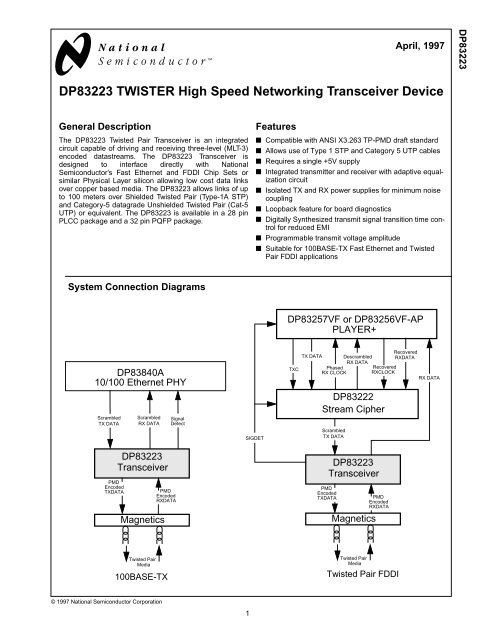
System Connection Diagrams<br />
DP83257VF or DP83256VF-AP<br />
PLAYER+<br />
DP83840A<br />
10/100 Ethernet PHY<br />
Scrambled<br />
TX DATA<br />
PMD<br />
Encoded<br />
TXDATA<br />
Scrambled<br />
RX DATA<br />
<strong>DP83223</strong><br />
<strong>Transceiver</strong><br />
Magnetics<br />
PMD<br />
Encoded<br />
RXDATA<br />
Signal<br />
Detect<br />
SIGDET<br />
TXC<br />
TX DATA<br />
Phased<br />
RX CLOCK<br />
DP83222<br />
Stream Cipher<br />
Scrambled<br />
TX DATA<br />
<strong>DP83223</strong><br />
<strong>Transceiver</strong><br />
PMD<br />
Encoded<br />
TXDATA<br />
Descrambled<br />
RX DATA<br />
Magnetics<br />
Recovered<br />
RXCLOCK<br />
PMD<br />
Encoded<br />
RXDATA<br />
Recovered<br />
RXDATA<br />
RX DATA<br />
Twisted Pair<br />
Media<br />
100BASE-TX<br />
Twisted Pair<br />
Media<br />
Twisted Pair FDDI<br />
© 1997 National Semiconductor Corporation<br />
1
General Description (Continued)<br />
Table of Contents<br />
1.0 Connection Diagram<br />
2.0 Pin Description<br />
3.0 Functional Description<br />
3.1 Overview<br />
3.2 MLT-3 Encoding<br />
3.3 Transition Time Control<br />
3.4 Adaptive Equalization<br />
3.5 Jitter Performance<br />
4.0 DC and AC Specifications<br />
4.1 TRANSMIT TIMING<br />
4.2 RECEIVE PROPAGATION DELAY<br />
4.3 LOOPBACK PROPAGATION DELAY<br />
4.4 SIGNAL DETECT TIMING<br />
4.5 ADAPTIVE EQUALIZER TIMING<br />
<strong>DP83223</strong><br />
Block Diagram<br />
TXREF<br />
PMRD+<br />
Programmable<br />
Current Output<br />
Driver<br />
LB<br />
TXO+<br />
PMRD-<br />
TXO-<br />
EQSEL<br />
PMID +<br />
RXI +<br />
RXI -<br />
CDET<br />
Equalizer Amp/<br />
Signal Detect<br />
DATA<br />
Comparators/<br />
Control Logic<br />
SD<br />
MUX LOGIC<br />
PMID -<br />
SD+<br />
LBEN<br />
SD-<br />
Revision A<br />
2
1.0 Connection Diagram<br />
<strong>DP83223</strong><br />
RXGND<br />
RXI+<br />
RXI-<br />
TXV CC<br />
TXREF<br />
TXGND<br />
TXO-<br />
TXO+<br />
TXGND<br />
TXV CC<br />
PMID+<br />
PMID-<br />
EXTV CC<br />
GND<br />
SD-<br />
SD+<br />
LBEN<br />
ENCSEL<br />
GND<br />
PMRD+<br />
PMRD-<br />
EQSEL<br />
CDET<br />
RXGND<br />
4 3 2 1 28 27 26<br />
5<br />
6<br />
25<br />
24<br />
7<br />
8<br />
9<br />
<strong>DP83223</strong>V<br />
23<br />
22<br />
21<br />
10<br />
11<br />
20<br />
19<br />
12 13 14 15 16 17 18<br />
V CC<br />
RXV CC<br />
RXV CC<br />
V CC<br />
28 Pin PLCC<br />
Order Number <strong>DP83223</strong>V<br />
See NS Package Number V28A<br />
RXGND<br />
RXI+<br />
RXI-<br />
TXREF<br />
TXGND<br />
PMID-<br />
TXO-<br />
TXO+<br />
EXTV CC<br />
GND<br />
TXGND<br />
SD-<br />
SD+<br />
N/C<br />
LBEN<br />
ENCSEL<br />
PMRD+<br />
PMRD-<br />
EQSEL<br />
CDET<br />
RXGND<br />
28 27 26<br />
25<br />
TXV CC<br />
1<br />
24<br />
2<br />
23<br />
3<br />
22<br />
4<br />
5<br />
<strong>DP83223</strong>VBE<br />
21<br />
20<br />
6<br />
19<br />
TXV CC<br />
7<br />
18<br />
8<br />
17<br />
9 10 11 12 13 14 15 16<br />
V CC<br />
GND<br />
N/C<br />
N/C<br />
RXV CC<br />
RXV CC<br />
V CC<br />
32 31 30<br />
29<br />
N/C<br />
PMID+<br />
32 Pin PQFP<br />
Order Number <strong>DP83223</strong>VBE<br />
See NS Package Number VBE32A<br />
3
2.0 Pin Description<br />
<strong>DP83223</strong> Pinout Summary<br />
<strong>DP83223</strong><br />
Symbol Pin No<br />
Type<br />
Description<br />
PLCC(PQFP)<br />
V CC 13,26 (10, 25) Supply Vcc: Positive power supply for the ECL compatible circuitry. The<br />
<strong>Transceiver</strong> operates from a single +5VDC power supply.<br />
GND 14, 22(11 ,20) Supply GND: Return path for the ECL compatible circuitry power supply.<br />
RXVcc 4, 27(26, 31) Supply Receive Vcc: Positive power supply for the small signal receive circuitry.<br />
This power supply is intentionally separated from others to eliminate<br />
receive errors due to coupled supply noise.<br />
RXGND 3, 28(27, 30) Supply Receive GND: Return path for the receive power supply circuitry. This<br />
power supply return is intentionally separated from others to eliminate<br />
receive errors due to coupled supply noise.<br />
TXVcc 5, 11(1, 7) Supply Transmit Vcc: Positive power supply required by the analog portion of the<br />
transmit circuitry. This power supply is intentionally separated from the<br />
others to prevent supply noise from coupling to the transmit outputs.<br />
TXGND 7, 10(3, 6) Supply Transmit GND: Return path for the analog transmit power supply circuitry.<br />
This supply return is intentionally separated from others to prevent supply<br />
noise from being coupled to the transmit outputs.<br />
EXTVcc 23(21) Supply External Vcc: Positive power supply for ECL output circuitry.<br />
RXI+/- 2, 1(29, 28) Differential Receive Data Inputs: Balanced differential line receiver inputs.<br />
Voltage In<br />
PMID+/- 25, 24(23, 22) ECL Out Physical Media Indicate Data: Differential ECL compatible outputs<br />
source the recovered receive data back to the Physical Layer device or to<br />
a separate clock recovery device.<br />
PMRD+/- 15, 16(12,13) ECL In Physical Media Request Data: Differential ECL compatible inputs which<br />
receive data from Physical Layer <strong>Device</strong>.<br />
TXO+/- 9, 8(5,4) Differential<br />
Current<br />
Out<br />
Transmit Data Outputs: Differential current driver outputs which drive<br />
MLT-3 encoded data over twisted pair cable. These outputs provide<br />
controlled rise and fall times designed to filter the transmitters output which<br />
helps to reduce associated EMI.<br />
SD+/- 20, 21(18, 19) ECL Out Signal Detect Outputs: Differential ECL compatible Signal Detect outputs<br />
indicating that either a signal with the proper amplitude is present at the<br />
RXI+/- inputs or that Loopback mode has been selected.<br />
TXREF 6(2) Current<br />
Out<br />
Transmit Amplitude Reference: Reference current pin allowing<br />
adjustment of TXO+/- transmit amplitude. By placing a resistor between<br />
this pin and GND, a reference current is setup which results in a given<br />
transmit amplitude for a given application. Refer to Functional Description<br />
in Section 3.1 for reference current equations.<br />
ENCSEL 12(9) CMOS In Encode Select Input: The TTL compatible CMOS Encode Select input<br />
controls the encoded state of the signal at the TXO+/- outputs. A logic low<br />
level at this input causes the TXO outputs to become MLT-3 encoded with<br />
the receiver programmed to accept MLT-3 encoded data. This is the<br />
recommended mode of operation. A logic high level causes the TXO pins<br />
to output standard two-level binary code and the receiver is conditioned to<br />
receive a two-level binary signal. The <strong>DP83223</strong>V does not guarantee this<br />
mode(binary) of operation.<br />
LBEN 19(17) CMOS In Loopback Enable: TTL compatible CMOS Loopback Enable input pin<br />
selects the internal loopback path which routes the PMRD+/- data to the<br />
PMID+/- differential outputs and forces Signal Detect true. During<br />
loopback, data present at the RXI+/- inputs is ignored. However, binary<br />
data is still transmitted by the TXO+/- outputs (regardless of the state of the<br />
ENCSEL input). Loopback mode is selected when LBEN is forced high.<br />
Normal operation occurs when LBEN is forced low.<br />
4
2.0 Pin Description (Continued)<br />
Symbol<br />
Pin No<br />
PLCC(PQFP)<br />
Type<br />
EQSEL 17(14) 3-Level Select<br />
Description<br />
Equalization Select: This three level Equalization Select input controls the<br />
mode of receiver equalization. Forcing a median voltage level,<br />
accomplished by allowing EQSEL to float, selects the adaptive<br />
equalization mode which automatically regulates the equalization effects<br />
based on signal degradation caused by the media. The other two levels are<br />
intended as test modes and are not a guaranteed mode of operation.<br />
Forcing a voltage less than 1.5V, selects full equalization which provides<br />
fixed equalization for a maximum length of cable. Forcing a voltage greater<br />
than 3.0V turns the receive equalizer off.<br />
CDET 18(15) CMOS In Cable Detect Bar: The active low Cable Detect CMOS input is provided to<br />
support the option of external Cable Detection circuitry (wire fault). With<br />
CDET low, the transceiver functions normally. With CDET high, the signal<br />
detect output is forced low which inhibits data reception by the PHY and<br />
the PMID outputs are forced to ECL static levels. The exception is in the<br />
case of Loopback when the Signal Detect output is forced high regardless<br />
of all other conditions. Please refer to the National Semiconductor Common<br />
Magnetics application note for further detail regarding the proper use<br />
of the <strong>DP83223</strong> in a 10/100 Ethernet application.<br />
<strong>DP83223</strong><br />
Revision A<br />
5
3.0 Functional Description<br />
3.1 Overview<br />
The <strong>DP83223</strong> transceiver consists of the major functional<br />
blocks shown in the “Block Diagram”. The Transmit section<br />
consists of an ECL input buffer for PMRD+/- and the<br />
Programmable Current Output Driver. The Programmable<br />
Current Output Driver can be configured to convert the<br />
incoming binary datastream to a current sourced MLT-3<br />
encoded datastream.<br />
The transmit amplitude of the signal presented at the TXO<br />
output pins can be controlled by varying the value of resistance<br />
between TXREF and GND. This TXREF resister,<br />
R REF , sets up a reference current which determines the<br />
final output current at TXO+/- as described by:<br />
I TXO = 20.48<br />
R REF<br />
encoding theoretically provides an additional 3dB reduction<br />
in EMI emissions depending on the measurement<br />
technique and system design/layout.<br />
The effect of MLT-3 encoding is the reduction of energy on<br />
the media in the critical frequency range of 20MHz to<br />
100MHz. This is achieved by trading line frequency for<br />
line voltage complexity. When a binary data stream is<br />
MLT-3 encoded, the result is a shift, in part, of some frequency<br />
components of the signal.<br />
See Figure 3-1, the second ‘high’ pulse in the binary<br />
waveform is transformed by an inversion to the ‘-1’ level in<br />
the MLT-3 waveform. This inversion corresponds to a certain<br />
decrease in energy from the original binary frequency<br />
component. The decrease in energy at the critical frequency<br />
of 62.5MHz is appreciable (3dB to 6dB).<br />
<strong>DP83223</strong><br />
The following equation yields the differential peak-peak<br />
transmit voltage for a given characteristic cable impedance:<br />
Binary<br />
1 0 1 0 0 1 1 0<br />
1 1<br />
V OUTpk-pkdiff = I TXO * Z cable<br />
2<br />
The transition times at the TXO+/- outputs are of special<br />
interest. These matched rise and fall times are digitally<br />
synthesized to reduce EMI emissions at the media interface<br />
and on the media. The controlled transition times<br />
also significantly reduce the design complexity and cost<br />
by minimizing external filtering.<br />
The Receive section consists of the following functional<br />
blocks: a differential input Equalization Amplifier with Signal<br />
Detect circuitry, signal Comparators with Control<br />
Logic, Loopback Multiplexer Logic, and differential ECL<br />
output drivers for PMID and Signal Detect.<br />
In adaptive or full equalization mode, as selected by the<br />
EQSEL input pin, the receive data is first equalized and<br />
then amplified for signal detection. If the receive equalizer<br />
is turned off, the data is then only amplified for signal<br />
detection.<br />
The Comparator and Control Logic Block performs several<br />
functions. Primarily, the comparators quantize and<br />
convert incoming MLT-3 into binary. The control logic<br />
receives input from CDET and ENCSEL enabling final signal<br />
detect indication and control of data conversion/regeneration.<br />
The Loopback Mux logic performs the function of routing<br />
the transmit data at the PMRD+/- inputs to either the<br />
PMID+/- pins (loopback enabled) or directly to the TXO+/-<br />
current outputs (normal operation).<br />
Finally, ECL output drivers are used to drive both PMID+/-<br />
receive data and SD+/- Signal Detect data to the appropriate<br />
Physical Layer device.<br />
3.2 MLT-3 Encoding<br />
The decision to incorporate MLT-3 (Multi-Level-Transmit /<br />
3 levels) signal encoding into the ANSI X3.263 Twisted<br />
Pair Standard is based solely on the issue of Electro-Magnetic<br />
Compatibility (EMC). Scrambling the datastream, via<br />
the Stream Cipher function, reduces EMI emissions at key<br />
frequencies by approximately 20dB. Although 20dB is significant,<br />
it may be insufficient to pass the FCC Class B<br />
radiation limit (with margin) for NRZI signalling at the standard<br />
transmit amplitude of 2.0V. The inclusion of MLT-3<br />
MLT-3<br />
Figure 3-1. Example of Binary vs. MLT-3<br />
The power spectrum plots in Figure 3-2 and Figure 3-3<br />
provide a clear comparison between scrambled binary<br />
and scrambled MLT-3 respectively. It should be noted that<br />
FCC Class B limits relate to radiated emissions and not<br />
the direct power spectrum. The plots in Figure 3-2 and<br />
Figure 3-3 are intended strictly for use as a general comparison<br />
between Binary and MLT-3 and should not be<br />
interpreted as absolute EMI performance indicators.<br />
10 dB / div<br />
1 0 -1 0 0 1 1 0 -1 -1<br />
0 MHz 125MHz 250MHz<br />
Figure 3-2. 1V Binary Power Spectrum<br />
Revision A<br />
6
3.0 Functional Description (Continued)<br />
10 dB / div<br />
0 MHz 125MHz 250MHz<br />
Figure 3-3. 2V MLT-3 Power Spectrum<br />
3.3 Transition Time Control<br />
The <strong>DP83223</strong> <strong>TWISTER</strong> incorporates a unique feature<br />
which virtually eliminates the need for external filtering of<br />
the transmitted signal. The transition times of the TXO<br />
output signals are digitally synthesized resulting in closely<br />
matched and controlled rise and fall times (Refer to Figure<br />
3-4). These controlled transition times, in conjunction<br />
with the associated magnetics, result in typical rise and<br />
fall times of greater than 3ns. These transition times lie<br />
within the range specified in the X3.263 Twisted Pair PMD<br />
standard.<br />
Figure 3-4. Controlled TXO Transitions<br />
3.4 Adaptive Equalization<br />
When transmitting data at high speeds over copper<br />
twisted pair cable, frequency dependent attenuation<br />
becomes a concern. In Twisted Pair Fast Ethernet or<br />
FDDI signalling the frequency content of the transmitted<br />
signal can vary greatly during normal operation based primarily<br />
on the randomness of the scrambled data stream.<br />
This variation in signal attenuation caused by frequency<br />
variations must be compensated for to ensure the integrity<br />
of the transmission.<br />
In order to ensure quality transmission when employing<br />
MLT-3 encoding, the compensation must be able to adapt<br />
to various cable lengths and cable types depending on the<br />
installed environment. In a fixed equalization system, the<br />
selection of long cable lengths for a given implementation,<br />
requires significant compensation which will over-compensate<br />
for shorter, lower attenuation lengths. Conversely,<br />
the selection of short or intermediate cable lengths requiring<br />
less compensation will cause serious under-compensation<br />
for longer length cables. Therefore, the<br />
compensation (equalization) must be adaptive to ensure<br />
proper conditioning of the received signal independent of<br />
cable length.<br />
The combination of choosing MLT-3 as the signal encoding<br />
scheme, in conjunction with a requirement for adaptive<br />
equalization, demands that compensation occur at the<br />
receive end of the transmission network. In order to implement<br />
receiver adaptive equalization, a known relationship<br />
between transmit output amplitude and a receive input<br />
reference must be specified and controlled. Nominal<br />
transmit output amplitude, as specified by the ANSI<br />
X3.263 TP-PMD document, is 2.0V peak to peak differential.<br />
The <strong>DP83223</strong> <strong>TWISTER</strong> incorporates a fixed nominal<br />
receive input reference. Given these two parameters, the<br />
adaptive equalization can determine the approximate<br />
cable length via signal attenuation at certain frequencies<br />
and actively compensate for cable length variations.<br />
Since the <strong>DP83223</strong> <strong>TWISTER</strong> transceiver’s receive input<br />
reference is fixed at approximately 1.45V and the transmit<br />
amplitude is fixed at 2.0V, an attenuation factor is<br />
required. This attenuation is accomplished by a simple<br />
resistive voltage divider placed at the RXI+/- inputs, which<br />
also serves as the forward termination for the transmission<br />
line (Refer to Figure 4-3). Because the voltage<br />
divider attenuates any noise along with the received signal,<br />
the Signal-to-Noise ratio is not decreased. An additional<br />
benefit is gained by including the voltage divider,<br />
where any insertion loss caused by the media coupling<br />
magnetics can be compensated for by adjusting the voltage<br />
divider ratio. This will ensure appropriate signal transfer<br />
and optimal adaptive equalization.<br />
For additional information regarding the interdependencies<br />
between the adaptive equalizer and the receive<br />
attenuation/termination circuit, refer to the NSC application<br />
note entitled “<strong>DP83223</strong> Adaptive Equalizer Considerations”.<br />
3.5 Jitter Performance<br />
This section briefly presents the typical jitter performance<br />
exhibited by the <strong>DP83223</strong> <strong>TWISTER</strong> transceiver. The<br />
<strong>DP83223</strong> <strong>TWISTER</strong> was subjected to the near worstcase<br />
condition of 110 Meters of Category 5 cable connected<br />
to two lengths of 10Meter cable via two 110<br />
punchdown blocks (totalling 130 Meters). The <strong>DP83223</strong><br />
<strong>DP83223</strong><br />
Revision A<br />
7
3.0 Functional Description (Continued)<br />
<strong>TWISTER</strong> was loaded with pseudo random data (PRBS-<br />
23) approximating actual packet data encrypted via the<br />
stream cipher algorithm. The typical peak-peak total jitter<br />
resulting from the combination of the transmitter, cable<br />
plant, and receiver is only 1.9ns Pk-Pk (MLT-3, room<br />
temp., nominal Vcc) as illustrated in Figure 3-5. Because<br />
the maximum eye opening is 8ns, The <strong>DP83223</strong> has little<br />
impact on the total jitter budget.<br />
<strong>DP83223</strong><br />
2ns / div<br />
Figure 3-5. MLT-3 Total Jitter=1.9ns Pk-Pk<br />
Revision A<br />
8
4.0 DC and AC Specifications<br />
Absolute Maximum Ratings<br />
Supply Voltage (V CC )<br />
-0.5 V to 7.0 V<br />
Recieved Power (RXV CC V)<br />
-0.5 V to 7.0 V<br />
Transmitted Power (RXV CC V) -0.5 V to 7.0V<br />
Storage Temperature Range (T STG ) -65 o C to 150 o C<br />
Power Dissipation (P D )<br />
1.575 W<br />
I ECl<br />
-50 mA<br />
Lead Temp. (T L ) (Soldering, 10 sec)<br />
260 o C<br />
ESD Rating<br />
(R ZAP = 1.5k, C ZAP = 120 pF)<br />
Recommended Operating Conditions<br />
2.0 KV<br />
Supply voltage (V DD ) 5 Volts + 5%<br />
Ambient Temperature (T A )<br />
0 to 70 o C<br />
Note: Absolute maximum ratings are those values beyond<br />
which the safety of the device cannot be guaranteed. They<br />
are not meant to imply that the device should be operated<br />
at these limits.<br />
<strong>DP83223</strong><br />
DC Specifications TA = 0 o C to 70 o C, VCC = 5 V 5%, unless otherwise specified<br />
Symbol Parameter Conditions Min Max Units<br />
I IHt TTL <strong>High</strong> Level Input V IN = Vcc 10 uA<br />
I ILt TTL Low Level Input V IN = GND -10 uA<br />
I IHcdet CDET <strong>High</strong> Level Input V IN = Vcc 10 uA<br />
I ILcdet CDET Low Level Input V IN = GND -10 uA<br />
I IHeqsel EQSEL <strong>High</strong> Level Input V IN = Vcc 800 uA<br />
I ILeqsel EQSEL Low Level Input V IN = GND -800 uA<br />
I IHe ECL <strong>High</strong> Level Input V IN = Vcc - 830 mV 50 uA<br />
I ILe ECL Low Level Input V IN = Vcc - 1570mV 1 uA<br />
V IHt TTL <strong>High</strong> Level Input 2 V<br />
V ILt TTL Low Level Input 0.8 V<br />
V IHcdet CDET <strong>High</strong> Level Input note 2 Vcc-1 V<br />
V ILcdet CDET Low Level Input note 2 1 V<br />
V IMeqsel EQSEL Mid Level Input note 3 Vcc / 2 V<br />
V IHe ECL <strong>High</strong> Level Input Vcc-<br />
1165<br />
V ILe ECL Low Level Input Vcc-<br />
1810<br />
V OHe ECL <strong>High</strong> Level Output Vcc-<br />
1075<br />
V OLe ECL Low Level Output Vcc-<br />
1860<br />
Vcc-880<br />
Vcc-<br />
1475<br />
Vcc-830<br />
Vcc-<br />
1570<br />
mV<br />
mV<br />
mV<br />
mV<br />
I CC Dynamic Supply Current notes 4 & 5, Figure 4-1 135 mA<br />
I TXO Transmit Current note 6, Figure 4-1 38.2 40 41.8 mA<br />
I TX-<br />
Omatch<br />
Transmit Current Matching note 7, Figure 4-1 -2 2 %<br />
SD THon Sig Det Assert Threshold note 8, Figure 4-2 700 mV<br />
SD THoff Sig Det De-assert Threshold notes 1 & 9, Figure 4-2 200 mV<br />
R INdiff RXI differential input resistance 7 9 KΩ<br />
9
4.0 DC and AC Specifications (Continued)<br />
Note 1:Guaranteed by characterization over process, temperature, and Vcc.<br />
Note 2:It is recommended that the CDET control input be tied directly to Vcc or GND to ensure proper operation. If CDET is to be driven from a gate, it is<br />
recommended that the gate be capable of true CMOS logic levels.<br />
Note 3:The median voltage level for EQSEL is normally accomplished by floating that pin.<br />
Note 4:ICC is a measure of total device current in normal MLT-3 mode with a 125Mb/s random data pattern applied to the PMRD+/- inputs to allow the<br />
TXO+/- outputs to switch at a nominal 2V pk-pk differential amplitude into a standard 50Ω differential load. ICC is minus the current through the PECL inputs.<br />
<strong>Device</strong> configuration: LBEN=0, CDET=0, ENCSEL=0, EQSEL=float, PMRD+/-=125Mb/s data, RXI+/-=125Mb/s data.<br />
Note 5:ICC does not include the current through the PECL outputs. Standard 50Ω Thevenin equivalent PECL terminations (figure 10) require approximately<br />
14 mA per pin, or a total of 56 mA. 100Ω PECL terminations require approximately 7 mA per pin, or a total of 28 mA. These external PECL termination current<br />
requirements should be considered when analyzing system power requirements.<br />
Note 6:TXO output current is a measure of the total differential current present at the TXO+/- outputs into a standard 50Ω differential load. <strong>Device</strong> configuration:<br />
R REF =510Ω, LBEN=0, CDET=0, ENCSEL=0, EQSEL=float, RXI+/-=static.<br />
Note 7:I TXOmatch refers to the percentage of mismatch in current between TXO+ and TXO- referenced to the total output current as defined by:<br />
<strong>DP83223</strong><br />
I TXOmatch =<br />
I TXO+ - I TXO-<br />
I TXO+ +I TXOx<br />
100<br />
<strong>Device</strong> configuration: R REF =510Ω, ENCSEL=0, PMRD+=0, PMRD-=1.<br />
Note 8:Signal Detect Assert Threshold is a measure of the pk-pk differential signal amplitude at the RXI+/- inputs of the RJ45 required to cause the Signal<br />
Detect differential output to assert. <strong>Device</strong> configuration: LBEN=0, CDET=0, ENCSEL=0, EQSEL=float, PMRD+/-=static, RXI+/-=125Mb/s data with swept<br />
amplitude.<br />
Note 9:Signal Detect De-assert Threshold is a measure of the pk-pk differential signal amplitude at the RXI+/- inputs of the RJ45 required to cause the Signal<br />
Detect differential output to de-assert. <strong>Device</strong> configuration: LBEN=0, CDET=0, ENCSEL=0, EQSEL=float, PMRD+/-=static, RXI+/-=125Mb/s data with<br />
swept amplitude<br />
ICC<br />
ICC external<br />
TXVCC RXVCC VCC EXTVCC<br />
+<br />
VCC<br />
-<br />
TXREF<br />
<strong>DP83223</strong><br />
SD+<br />
SD-<br />
PMID+<br />
PMID-<br />
510Ω<br />
TXGND RXGND GND<br />
TXO+ TXO-<br />
50Ω<br />
50Ω 50Ω<br />
50Ω<br />
25Ω<br />
25Ω<br />
+<br />
VCC - 2V<br />
-<br />
Figure 4-1. ICC / Load Diagram<br />
10
4.0 DC and AC Specifications (Continued)<br />
<strong>DP83223</strong><br />
Active PMID<br />
Inactive PMID<br />
SD THoff<br />
SD THon<br />
Post Equalized Signal Detect Voltage<br />
Figure 4-2. Post Equalized Signal Detect Voltage<br />
V CC<br />
Data from<br />
PHY<br />
<strong>Device</strong><br />
SD To PHY<br />
<strong>Device</strong><br />
Data to PHY or<br />
Clock Recovery<br />
<strong>Device</strong><br />
0.01uF<br />
float<br />
VCC<br />
PMRD+<br />
PMRD-<br />
SD+<br />
SD-<br />
PMID+<br />
PMID-<br />
EQSEL<br />
ENCSEL<br />
CDET<br />
LBEN<br />
GND<br />
<strong>DP83223</strong><br />
EXTVCC<br />
VCC<br />
TXVCC<br />
TXO+<br />
RXVCC<br />
RXI+<br />
TXO-<br />
RXI-<br />
RXGND<br />
TXGND<br />
TXREF<br />
FB<br />
50Ω<br />
0.01uF<br />
50Ω<br />
12.1Ω 12.1Ω<br />
37.9Ω 37.9Ω<br />
Contact National Semiconductor<br />
for further information relating to<br />
available magnetics modules<br />
Transmit<br />
Magnetics<br />
Receive<br />
Magnetics<br />
1<br />
2<br />
3<br />
4<br />
5<br />
6<br />
7<br />
8<br />
RJ-45<br />
The Receive Attenuation / Termination network<br />
must be optimized to compensate for the insertion<br />
loss of the receive magnetics.<br />
Please refer to the National Semiconductor Application Note<br />
entitled “<strong>DP83223</strong> Adaptive Equalization Considerations”<br />
for further detail. The values provided in this example<br />
are targeted to match an insertion loss of approximately<br />
0.4dB (approximately 90mV pk-pk differential of loss for<br />
a typical scrambled IDLE line state) which will result in<br />
a final amplitude of approximately 1.45V pk-pk differential<br />
as seen across the RXI+/- inputs for zero Meters of cable.<br />
0.01uF<br />
R REF<br />
*510Ω<br />
Common Mode Noise Filter<br />
GND<br />
*The Rref resistor value may need to be adjusted<br />
to compensate for transmit magnetics insertion<br />
loss in order to achieve the standard specific<br />
2.0V pk-pk differential TXO+/- output amplitude<br />
as measured across the RJ45 transmit pins.<br />
The PMRD, SD and PMID 100K ECL differential signal must be<br />
terminated into a standard ECL load of 50Ω to VCC-2.0V or equivalent:<br />
i.e. Thevenin of 130Ω to GND accompanied by 82Ω to VCC<br />
All resistors are 1/10th Wt, 1% tolerance<br />
All capacitors are 16V ceramic<br />
FB<br />
= Murata # BLM31A02PT (1206 package)<br />
Figure 4-3. Typical Schematic for 100BASE-TX signalling over Cat-5 UTP 100Ω cable<br />
11
4.0 DC and AC Specifications (Continued)<br />
4.1 TRANSMIT TIMING<br />
<strong>DP83223</strong><br />
PMRD+<br />
1<br />
0<br />
-1<br />
PMID-<br />
PMRD-<br />
T1.3 T1.1 T1.1<br />
10% - 90%<br />
TXO+<br />
TXO-<br />
TXO-<br />
TXO+<br />
Number Parameter Min Typ Max Units<br />
T1.1 TXO Output Rise and Fall 2.25 2.75 3.25 ns<br />
T1.2 TXO Rise / Fall Symmetry 500 ps<br />
T1.3 TX prop delay 7 ns<br />
T1.4 Transmit Jitter 1.4 ns<br />
Note: TXO Output Rise and Fall time is a measure of the transition time for all MLT-3 transitions from 10% to 90%. This measurement is conducted directly<br />
at the TXO+/- outputs and does not include the additional bandwidth limiting effects of an isolation transformer. Each of the four possible MLT-3 transitions<br />
is measured (see figure 2 for MLT-3 waveform example). The TXO+/- outputs are configured to switch at a nominal 2V pk-pk differential amplitude into a<br />
standard 50Ω differential load. <strong>Device</strong> configuration: LBEN=0, CDET=0, ENCSEL=0, EQSEL=float, PMRD+/-=125Mb/s data, RXI+/-=static.<br />
Note: : t TXr/fsym TXO Rise and Fall Symmetry is the difference between the maximum and minimum of all rise and fall times. <strong>Device</strong> configuration: LBEN=0,<br />
CDET=0, ENCSEL=0, EQSEL=float, PMRD+/-=125Mb/s data, RXI+/-=static.<br />
Note: : The Transmit channel propagation delay is a measure of the time delay imposed on the transmit data as it passes from the PMRD+/- inputs to the<br />
TXO+/- outputs. <strong>Device</strong> configuration: LBEN=0, CDET=0, ENCSEL=0, EQSEL=float, PMRD+/-=125Mb/s data, RXI+/-=static.<br />
Note: Transmit Jitter is a measure of the total jitter as measured differentially across the TXO+/- outputs of the device. This includes the cumulative effect<br />
of Duty Cycle Distortion (DCD), Data Dependent Jitter (DDJ), and Random Jitter (RJ). <strong>Device</strong> configuration: LBEN=0, CDET=0, ENCSEL=0, EQSEL=float,<br />
PMRD+/-=125Mb/s data (pseudo random ^15), RXI+/-=125Mb/s data in order to induce a worst case system level noise environment.<br />
Note: T1.1, T1.2 and T1.4 are guaranteed by characterization over process, temperature, and Vcc.<br />
4.2 RECEIVE PROPAGATION DELAY<br />
RXI+<br />
PMID+<br />
T2.1<br />
RXI-<br />
Number Parameter Min Typ Max Units<br />
T2.1 Receive Propagation Delay 7 ns<br />
Note: The Receive channel propagation delay is a measure of the time delay imposed on the receive data as it passes from the RXI+/- inputs to the PMID+/-<br />
outputs. This measurement is taken after the device has had sufficient time for the receive adaptive equalizer to converge. <strong>Device</strong> configuration: LBEN=0,<br />
CDET=0, ENCSEL=0, EQSEL=float, PMRD+/-=static, RXI+/-=125Mb/s data.<br />
12
4.3 LOOPBACK PROPAGATION DELAY<br />
PMRD+<br />
PMID+<br />
T3.1<br />
PMRD-<br />
PMID-<br />
Number Parameter Min Typ Max Units<br />
T3.1 Loopback Propagation Delay 7 ns<br />
4.4 SIGNAL DETECT TIMING<br />
RXI +/-<br />
static<br />
signal<br />
static<br />
T4.1 T4.2<br />
Do Not Use<br />
SD+<br />
Number Parameter Min Typ Max Units<br />
T4.1 Signal Detect Turn-On Time 40 100 us<br />
T4.2 Signal Detect Turn-Off Time 12 50 us<br />
Note: The Signal Detect Assert Time is a measure of the time required for Signal Detect to assert after the RXI+/- inputs are provided with a receive signal<br />
with sufficient amplitude to meet the Signal Detect Assert Threshold parameter. <strong>Device</strong> configuration: LBEN=0, CDET=0, ENCSEL=0, EQSEL=float, PM-<br />
RD+/-=static, RXI+/-=125Mb/s data with amplitude greater than 700mV pk-pk differential.<br />
Note: The Signal Detect De-assert Time is a measure of the time required for Signal Detect to deassert after the RXI+/- inputs are provided with a receive<br />
signal with sufficient amplitude to meet the Signal Detect Deassert Threshold parameter. <strong>Device</strong> configuration: LBEN=0, CDET=0, ENCSEL=0,<br />
EQSEL=float, PMRD+/-=static, RXI+/-=125Mb/s data with amplitude less than 200mV pk-pk differential.<br />
4.5 ADAPTIVE EQUALIZER TIMING<br />
Number Parameter Min Typ Max Units<br />
T5.1 Total Jitter (TX+RX) 2 3.5 ns<br />
Note: Total Receive Jitter is a measure of the total accumulated jitter as measured differentially across the PMID+/- receive outputs of the device. This parameter<br />
is guaranteed by an ATE adaptive equalizer jitter measurement (done at worst case conditions) and a system level characterization over temperature<br />
and Vcc. The ATE measurement has been empirically correlated with the system level jitter measurement, which includes all transmit jitter (as described in<br />
T1.3) as well as all jitter induced by a worst case Cat-5 cable plant and the additional Jitter induced by the receive operation of the device. <strong>Device</strong> configuration:<br />
LBEN=0, CDET=0, ENCSEL=0, EQSEL=float, PMRD+/-=125Mb/s data, RXI+/-=125Mb/s data.
LIFE SUPPORT POLICY<br />
NATIONAL'S PRODUCTS ARE NOT AUTHORIZED FOR USE AS CRITICAL COMPONENTS IN LIFE SUPPORT<br />
DEVICES OR SYSTEMS WITHOUT THE EXPRESS WRITTEN APPROVAL OF THE PRESIDENT OF NATIONAL<br />
SEMICONDUCTOR CORPORATION. As used herein:<br />
1. Life support devices or systems we do or systems<br />
which, (a) are intended for surgical implant into the<br />
body, or (b) support or sustain life, and whose failure to<br />
perform, when properly used in accordance with<br />
instructions for use provided in the labeling, can be<br />
reasonably expected to result in a significant injury to<br />
the user.<br />
2. A critical component is any component of a life support<br />
device or system whose failure to perform can be<br />
reasonably expected to cause the failure of the life support<br />
device or system, or to affect its safety or effectiveness.<br />
National Semiconductor<br />
Corporation<br />
National Semiconductor<br />
Corporation<br />
Europe<br />
Fax:(+49) 0-180-530 85 86<br />
Email:cnjwge@tevm2.nsc.com<br />
Duetsch Tel: (+49) 0-180-530 85 86<br />
English Tel: (+49) 0-180-532 78 32<br />
Francais Tel: (+49) 0-180-532 93 58<br />
Italiano Tel: (+49) 0-180-534 16 80<br />
National Semiconductor<br />
Corporation<br />
Japan Ltd.<br />
Tel: 81-043-299-2308<br />
Fax: 81-043-299-2408<br />
National Semiconductor<br />
Corporation<br />
Hong Kong Ltd.<br />
13th Floor, Straight Block,<br />
Ocean Centre, 5 Canton Rd.<br />
Tsimshatsui, Kowloon<br />
Hong Kong<br />
Tel: (852) 2737-1600<br />
Fax: (852) 2736-9960<br />
1111 West Bardin Road<br />
Arlington, TX 76017<br />
Tel: 1(800) 272-9959<br />
Fax: 1(800) 737-7018<br />
Do Not Use