Application Note for FSA03 FALCOM Smart Antenna
Application Note for FSA03 FALCOM Smart Antenna
Application Note for FSA03 FALCOM Smart Antenna

Create successful ePaper yourself
Turn your PDF publications into a flip-book with our unique Google optimized e-Paper software.
This document is available at HTTP://WWW.<strong>FALCOM</strong>.DE/<br />
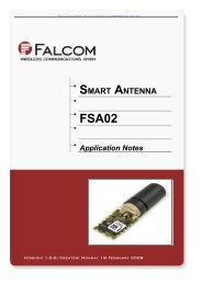
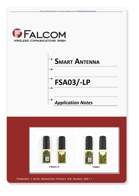
SMART ANTENNA<br />
<strong>FSA03</strong>/-LP<br />
<strong>Application</strong> <strong>Note</strong>s<br />
Version: 1.0.5; Modified: Friday 25 March 2011
<strong>FALCOM</strong> SMART ANTENNAS <strong>FSA03</strong>/-LP VERSION 1.0.5<br />
Table of contents<br />
1 INTRODUCTION....................................................................................3<br />
1.1 GENERAL..................................................................................................................................3<br />
1.2 TECHNICAL DATA (IN BRIEF).............................................................................................................3<br />
1.3 SIGNAL LEVELS............................................................................................................................3<br />
2 SECURITY..............................................................................................5<br />
2.1 ELECTROSTATIC DISCHARGE (ESD)....................................................................................................5<br />
2.2 SOLDERING METHOD.....................................................................................................................5<br />
3 SCHEMATICS.........................................................................................6<br />
Version history:<br />
This table provides a summary of the document revisions.<br />
Number Author Changes Modified<br />
1.0.5 F. Beqiri - USB interface is now supported. 25/03/2011<br />
1.0.4 F. Beqiri - Picture changed to the <strong>FSA03</strong> new hardware verson 02b and added <strong>for</strong> <strong>FSA03</strong>-LP. Power<br />
consumptions <strong>for</strong> both modules added.<br />
1.0.3 F. Beqiri - Maximum input voltage at VBATT pin changed from 4.8 V to 3.6 V - see Table 1 in chapter 1.3.<br />
- Baud Rate Option: 38400 bps<br />
- Added new Side-view <strong>for</strong> Hardware revision 02b and higher.<br />
09/11/2010<br />
14/09/2010<br />
1.0.2 F. Beqiri - Added side view 18/02/2010<br />
1.0.1 F. Beqiri - Updated chapter "Soldering method" 05/05/2009<br />
1.0.0 F. Beqiri - Initial version 07/10/2008<br />
This confidential document is a property of <strong>FALCOM</strong> and may not be copied or circulated without previous permission.<br />
Page 2
<strong>FALCOM</strong> SMART ANTENNAS <strong>FSA03</strong>/-LP VERSION 1.0.5<br />
1 INTRODUCTION<br />
This application note comprises a brief description of the operation of the <strong>FALCOM</strong> <strong>Smart</strong><br />
<strong>Antenna</strong>s <strong>FSA03</strong> and <strong>FSA03</strong>-LP, the Pad-Design and an application circuit.<br />
1.1 General<br />
The <strong>Smart</strong> <strong>Antenna</strong> operates from internal ROM.<br />
1.2 Technical data (in brief)<br />
The <strong>FSA03</strong> architecture is based on the UBX-G5010 and <strong>FSA03</strong>-LP on UBX-G6010 the single chip from ublox,<br />
<strong>for</strong> more in<strong>for</strong>mation about both chips and the u-blox5/6 protocol specifications, please refer to<br />
the u-blox website: www.u-blox.com<br />
� Temperature Range:<br />
� Power Consumption:<br />
� Directive:<br />
� ROM:<br />
➢ Operation: -40 to 85°C.<br />
➢ <strong>FSA03</strong>: avarage. 43 mA @ 3.3 V DC; Temp. 23° C.<br />
➢ <strong>FSA03</strong>-LP: avarage. 43 mA @ 3.3 V DC; Temp. 23° C.<br />
➢ RoHS compliant (lead-free) and green (no halogens).<br />
➢ Output NMEA messages.<br />
- Baudrate: (default=9600 bps; option=38400),<br />
- RMC, GGA, GSA, GSV, VTG, GLL<br />
This confidential document is a property of <strong>FALCOM</strong> and may not be copied or circulated without previous permission.<br />
Page 3
<strong>FALCOM</strong> SMART ANTENNAS <strong>FSA03</strong>/-LP VERSION 1.0.5<br />
1.3 Signal levels<br />
The names and position of the pads can be seen from the Pad-Design, which is added in<br />
chapter 3, “Schematics“. The NC-pins in this schematic are not connected.<br />
Pin name Level Function<br />
RES 3.3 V CMOS Input<br />
TM 3.3 V CMOS Output<br />
VBATT 1.4 V – 3.6 VDC Input<br />
GND 0 V -<br />
VCC 3.3 VDC ±5 % Input<br />
GND 0 V -<br />
USB_DM 3.3 V USB Data Line Minus<br />
USB_DP 3.3 V USB Data Line Plus<br />
VDD_USB 3.3 VDC ±5 % Supply voltage <strong>for</strong> internal USB-Transceiver<br />
TX 3.3 V CMOS Output<br />
RX 3.3 V CMOS Input<br />
Table 1: Signal levels and their function<br />
This confidential document is a property of <strong>FALCOM</strong> and may not be copied or circulated without previous permission.<br />
Page 4
<strong>FALCOM</strong> SMART ANTENNAS <strong>FSA03</strong>/-LP VERSION 1.0.5<br />
2 SECURITY<br />
This chapter contains important in<strong>for</strong>mation <strong>for</strong> the safe and reliable use of the GPS receiver.<br />
Please read this chapter carefully be<strong>for</strong>e starting to use this GPS receiver.<br />
2.1 Electrostatic Discharge (ESD)<br />
The <strong>FSA03</strong>/-LP <strong>Smart</strong> <strong>Antenna</strong>s contain class 1 devices. The <strong>FSA03</strong>/-LP <strong>Smart</strong> <strong>Antenna</strong>s contain<br />
components that can be damaged or destroyed by electrostatic discharge. When handling the<br />
modules, observe the necessary safety precautions against electrostatic discharge (ESD), in<br />
accordance with EN 61340-5-1 and the following. The following Electrostatic Discharge (ESD)<br />
precautions are recommended:<br />
• Protective outer garments.<br />
• Handle device in ESD safeguarded work area.<br />
• Transport device in ESD shielded containers.<br />
• Monitor and test all ESD protection equipment.<br />
• Treat the <strong>FSA03</strong>/-LP <strong>Smart</strong> <strong>Antenna</strong> sas extremely sensitive to ESD.<br />
2.2 Soldering method<br />
The <strong>FSA03</strong>/-LP <strong>Smart</strong> <strong>Antenna</strong>s must be soldered only manually with a soldering iron. The<br />
soldered connection / pad design should be in accordance with IPC-A-610D - Chapter 8.2.4.<br />
References<br />
Customers may refer to following IPC standard <strong>for</strong> more details:<br />
➢ IPC-A-610D chapter 8.2.4, "Castellated Terminations".<br />
This confidential document is a property of <strong>FALCOM</strong> and may not be copied or circulated without previous permission.<br />
Page 5
VDD_USB<br />
USB_DP<br />
USB_DM
Top View<br />
VDD_USB USB_DP USB_DM
Side View<br />
(Hardware Revision 02b and higher)
Side View<br />
(Hardware Revision 02a and lower)
1<br />
1<br />
2<br />
2<br />
3<br />
3<br />
4<br />
C1<br />
VCC<br />
A 100nF<br />
A<br />
J1<br />
C2 C3<br />
DB9<br />
SKT<br />
1<br />
6<br />
2<br />
7<br />
3<br />
8<br />
4<br />
9<br />
5<br />
BLM11<br />
R1<br />
BLM11<br />
R3<br />
100nF<br />
TXA_RS232<br />
RXA_RS232<br />
C4<br />
100nF<br />
100nF<br />
3<br />
7<br />
13<br />
8<br />
2<br />
4<br />
5<br />
6<br />
C5<br />
100nF<br />
MAX3221<br />
P228_Rev01a<br />
B R10 0R#<br />
B<br />
TP2<br />
U2<br />
MIC5205<br />
TP3<br />
1<br />
C<br />
J3<br />
1<br />
2<br />
3<br />
4<br />
STVB_1mm_NOKIA<br />
VC5<br />
C8<br />
100nF<br />
1<br />
3<br />
IN<br />
EN<br />
OUT<br />
5<br />
R12<br />
10k<br />
C6<br />
33UF/4V<br />
VCC<br />
C7<br />
220nF<br />
2<br />
J2<br />
ML621S/F9D<br />
R11<br />
750R<br />
D2<br />
MBR0520<br />
VCC<br />
C<br />
GND<br />
2<br />
ADJ<br />
4<br />
R9 0R#<br />
R13<br />
18k<br />
U3<br />
EN 1<br />
V+<br />
V-<br />
C1+<br />
C1-<br />
C2+<br />
C2- GND 14<br />
T1IN 11<br />
FORCEON 12<br />
T1OUT<br />
INVALID 10<br />
VCC<br />
R1IN R1OUT<br />
9<br />
15<br />
FORCEOFF<br />
16<br />
C9<br />
470pF<br />
D D<br />
TP_N1<br />
4<br />
TP4<br />
100R<br />
100R<br />
VCC<br />
Justiermarken<br />
JUST1<br />
JUST2<br />
5<br />
R2<br />
R4<br />
5<br />
TXA<br />
RXA<br />
R7<br />
0R<br />
Title<br />
6<br />
U1<br />
9<br />
USB_DM<br />
7<br />
VCC<br />
USB_DP<br />
10 VDD_USB<br />
12<br />
TX<br />
11<br />
RX<br />
13<br />
USB_DP<br />
USB_DM<br />
<strong>FALCOM</strong><br />
Gewerbering 6<br />
98704 Langewiesen<br />
RES 1<br />
NC 2<br />
NC 3<br />
TM 4<br />
VBATT<br />
5<br />
GND 6<br />
GND 8<br />
2<br />
1<br />
VBATT<br />
SW2<br />
SW DIP-2<br />
<strong>FSA03</strong> - <strong>Application</strong>-Circuitry<br />
Date: Monday, August 11, 2008 Sheet 1 of 1<br />
6<br />
7<br />
8<br />
7<br />
SW1<br />
SW SPST<br />
R6<br />
470R<br />
D1<br />
LED<br />
VBATT<br />
Size Document Number R ev<br />
A<br />
01b<br />
8