XF55-AVL Hardware description Preliminary - Falcom
XF55-AVL Hardware description Preliminary - Falcom
XF55-AVL Hardware description Preliminary - Falcom

Create successful ePaper yourself
Turn your PDF publications into a flip-book with our unique Google optimized e-Paper software.
Version 0.01<br />
This document is available at HTTP://WWW.FALCOM.DE/ .<br />
<strong>XF55</strong>-<strong>AVL</strong><br />
<strong>Hardware</strong> <strong>description</strong><br />
<strong>Preliminary</strong>
<strong>XF55</strong>-<strong>AVL</strong> HARDWARE DESCRIPTION VERSION 0.01<br />
Index of contents<br />
0 INTRODUCTION ..............................................................6<br />
0.1 GENERAL........................................................................................................................................ 6<br />
0.2 CIRCUIT CONCEPT........................................................................................................................... 7<br />
0.3 USED ABBREVIATIONS.................................................................................................................... 9<br />
0.4 RELATED DOCUMENTS.................................................................................................................. 11<br />
1 SECURITY .......................................................................12<br />
1.1 GENERAL INFORMATION............................................................................................................... 12<br />
1.2 EXPOSURE TO RF ENERGY............................................................................................................ 12<br />
1.3 EFFICIENT MODEM OPERATION..................................................................................................... 12<br />
1.4 ANTENNA CARE AND REPLACEMENT ............................................................................................ 13<br />
1.5 DRIVING ....................................................................................................................................... 13<br />
1.6 ELECTRONIC DEVICES................................................................................................................... 13<br />
1.7 VEHICLE ELECTRONIC EQUIPMENT ............................................................................................... 13<br />
1.8 MEDICAL ELECTRONIC EQUIPMENT .............................................................................................. 13<br />
1.9 AIRCRAFT..................................................................................................................................... 13<br />
1.10 CHILDREN .................................................................................................................................... 14<br />
1.11 BLASTING AREAS.......................................................................................................................... 14<br />
1.12 POTENTIALLY EXPLOSIVE ATMOSPHERES ..................................................................................... 14<br />
1.13 NON-IONIZING RADIATION............................................................................................................ 14<br />
2 SAFETY STANDARDS...................................................15<br />
3 TECHNICAL DATA........................................................16<br />
3.1 GENERAL SPECIFICATIONS OF MODULE <strong>XF55</strong>-<strong>AVL</strong> ..................................................................... 16<br />
3.1.1 Power consumption ..................................................................................................................... 16<br />
3.2 TECHNICAL SPECIFICATIONS OF GSM/GPRS ENGINE................................................................... 18<br />
3.3 TECHNICAL SPECIFICATIONS OF GPS RECEIVER ........................................................................... 20<br />
4 GSM/GPRS APPLICATION INTERFACE..................23<br />
4.1 DESCRIPTION OF OPERATING MODES ............................................................................................ 23<br />
4.1.1 Normal mode operation ............................................................................................................... 23<br />
4.1.1.1 GSM/GPRS SLEEP ...................................................................................................................................... 23<br />
4.1.1.2 GSM IDLE.................................................................................................................................................... 23<br />
4.1.1.3 GSM TALK................................................................................................................................................... 23<br />
4.1.1.4 GPRS IDLE .................................................................................................................................................. 23<br />
4.1.1.5 GPRS DATA................................................................................................................................................. 24<br />
4.1.2 Power down ................................................................................................................................. 24<br />
4.1.3 Alarm mode ................................................................................................................................. 24<br />
4.1.4 Charge-only mode ....................................................................................................................... 24<br />
4.1.5 Charge mode during normal operation ........................................................................................ 24<br />
4.2 DESCRIPTION OF THE 80-PIN DOUBLE-ROW CONNECTOR .............................................................. 24<br />
4.3 DESCRIPTION OF THE 50-PIN DOUBLE-ROW CONNECTOR .............................................................. 28<br />
4.3.1 Special pin <strong>description</strong>................................................................................................................. 32<br />
4.3.1.1 Power supply................................................................................................................................................ 32<br />
4.3.1.2 Power supply pins (41…50, 53, and 54) on the board-to-board connectors................................................ 32<br />
4.3.1.3 Minimizing power losses .............................................................................................................................. 33<br />
4.3.1.4 Monitoring power supply ............................................................................................................................. 34<br />
4.3.2 Power up/down scenarios ............................................................................................................ 34<br />
4.3.2.1 Turn on the GSM/GPRS part of <strong>XF55</strong>-<strong>AVL</strong> ................................................................................................. 34<br />
4.3.2.2 Turn on the GSM/GPRS part of <strong>XF55</strong>-<strong>AVL</strong> using the ignition line GSM_IGT (Power on).......................... 34<br />
4.3.2.3 Timing of the ignition process ...................................................................................................................... 35<br />
4.3.2.4 Turn on the GSM/GPRS part of <strong>XF55</strong>-<strong>AVL</strong> using the GSM_POWER signal ............................................... 36<br />
4.3.2.5 Turn on the GSM/GPRS part of <strong>XF55</strong>-<strong>AVL</strong> using the RTC (Alarm mode)................................................... 36<br />
4.3.3 Turn off the GSM/GPRS part of <strong>XF55</strong>-<strong>AVL</strong> .............................................................................. 37<br />
4.3.3.1 Turn off GSM/GPRS part of the <strong>XF55</strong>-<strong>AVL</strong> module using AT command ..................................................... 38<br />
This confidential document is a property of FALCOM GmbH and may not be copied or circulated without previous permission.<br />
Page 1
<strong>XF55</strong>-<strong>AVL</strong> HARDWARE DESCRIPTION VERSION 0.01<br />
4.3.3.2 Maximum number of turn-on/turn-off cycles................................................................................................ 38<br />
4.3.3.3 Emergency shutdown using GSM_EMERGOFF pin.................................................................................... 38<br />
4.3.4 Automatic shutdown.................................................................................................................... 39<br />
4.3.4.1 Temperature dependent shutdown................................................................................................................ 40<br />
4.3.4.2 Temperature control during emergency call ................................................................................................ 41<br />
4.3.4.3 Under voltage shutdown if battery NTC is present....................................................................................... 41<br />
4.3.4.4 Under voltage shutdown if no battery NTC is present.................................................................................. 41<br />
4.3.4.5 Over voltage shutdown................................................................................................................................. 41<br />
4.4 AUTOMATIC GPRS MULTISLOT CLASS CHANGE.......................................................................... 42<br />
4.5 GSM CHARGING CONTROL........................................................................................................... 42<br />
4.5.1 Battery pack characteristics ......................................................................................................... 43<br />
4.5.2 Recommended battery pack specification ................................................................................... 45<br />
4.5.3 Implemented charging technique................................................................................................. 45<br />
4.5.3.1 Trickle charging........................................................................................................................................... 45<br />
4.5.3.2 Fast charging ............................................................................................................................................... 46<br />
4.5.4 Operating modes during charging................................................................................................ 47<br />
4.5.4.1 Comparison Charge-only and Charge mode................................................................................................ 47<br />
4.5.5 Charger requirements................................................................................................................... 48<br />
4.6 POWER SAVING............................................................................................................................. 49<br />
4.6.1 No power saving (AT+CFUN=1)................................................................................................ 49<br />
4.6.2 NON-CYCLIC SLEEP mode (AT+CFUN=0) ............................................................................ 49<br />
4.6.3 CYCLIC SLEEP mode (AT+CFUN=5, 6, 7, 8) .......................................................................... 49<br />
4.6.4 CYCLIC SLEEP mode AT+CFUN=9......................................................................................... 50<br />
4.6.5 Timing of the GSM_CTS signal in CYCLIC SLEEP modes ...................................................... 50<br />
4.6.6 Wake up <strong>XF55</strong>-<strong>AVL</strong> from SLEEP mode .................................................................................... 52<br />
4.7 SUMMARY OF STATE TRANSITIONS (EXCEPT SLEEP MODE)......................................................... 53<br />
4.8 RTC BACKUP FOR GSM/GPRS PART OF <strong>XF55</strong>-<strong>AVL</strong>................................................................... 54<br />
4.9 FEATURES SUPPORTED ON THE SERIAL INTERFACE OF GSM/GPRS PART..................................... 55<br />
4.10 AUDIO INTERFACES ...................................................................................................................... 56<br />
4.10.1 Microphone circuit....................................................................................................................... 57<br />
4.10.2 Speech processing........................................................................................................................ 58<br />
4.10.3 DAI timing................................................................................................................................... 58<br />
4.10.4 SIM interface ............................................................................................................................... 60<br />
4.10.4.1 Requirements for using the GSM_CCIN pin ................................................................................................ 60<br />
4.10.4.2 Design considerations for SIM card holder ................................................................................................. 61<br />
4.11 CONTROL SIGNALS ....................................................................................................................... 63<br />
4.11.1 Inputs ........................................................................................................................................... 63<br />
4.11.2 Outputs ........................................................................................................................................ 63<br />
4.11.2.1 Synchronization signal ................................................................................................................................. 63<br />
4.11.2.2 Using the GSM_SYNC pin to control a status LED...................................................................................... 64<br />
4.11.2.3 Behaviour of the GSM_RING0 line (ASC0 interface only)...........................................................................65<br />
5 GPS APPLICATION INTERFACE...............................67<br />
5.1 SIGNAL PROCESSING OPERATION OF GPS RECEIVER.................................................................... 67<br />
5.2 DESCRIPTION OF OPERATING MODES ............................................................................................ 68<br />
5.2.1 Normal Operation ........................................................................................................................ 68<br />
5.2.2 Trickle Power Operation.............................................................................................................. 68<br />
5.2.3 Push-to-Fix Mode ........................................................................................................................ 70<br />
5.3 NMEA INPUT MESSAGE FOR TRICKLE POWER MODE................................................................... 70<br />
5.4 INTEGRATED GPS RECEIVER ARCHITECTURE .............................................................................. 72<br />
5.4.1 Description of GPS receiving signals .......................................................................................... 73<br />
5.5 GPS INPUT SIGNALS ..................................................................................................................... 73<br />
5.6 CONFIGURATION AND TIMING SIGNALS ........................................................................................ 74<br />
5.6.1 Serial communication signals ...................................................................................................... 75<br />
5.6.2 General purpose input/output....................................................................................................... 76<br />
5.6.3 General purpose input.................................................................................................................. 76<br />
5.6.4 General purpose Output............................................................................................................... 77<br />
6 HARDWARE INTERFACES .........................................78<br />
6.1 DETERMINING THE EXTERNAL EQUIPMENT TYPE......................................................................... 78<br />
6.2 INTERFACES OVERVIEW................................................................................................................ 79<br />
This confidential document is a property of FALCOM GmbH and may not be copied or circulated without previous permission.<br />
Page 2
<strong>XF55</strong>-<strong>AVL</strong> HARDWARE DESCRIPTION VERSION 0.01<br />
6.2.1 Interface A (80-pin board to board connector) ............................................................................ 80<br />
6.2.2 Interface B (50-pin board to board connector)............................................................................. 80<br />
6.2.3 Interface C (GSM antenna installation) ....................................................................................... 81<br />
6.2.3.1 GSM antenna connector............................................................................................................................... 81<br />
6.2.4 Interface D (GPS antenna interface)............................................................................................ 81<br />
6.2.5 Interface E (Mounting holes)....................................................................................................... 82<br />
7 ELECTRICAL, RELIABILITY AND RADIO<br />
CHARACTERISTICS .....................................................84<br />
7.1 ABSOLUTE MAXIMUM RATINGS .................................................................................................... 84<br />
7.2 OPERATING TEMPERATURES......................................................................................................... 84<br />
7.3 ELECTRICAL CHARACTERISTICS OF THE VOICE BAND PART .......................................................... 85<br />
7.3.1 Setting audio parameters by AT commands ................................................................................ 85<br />
7.3.2 Audio programming model.......................................................................................................... 85<br />
7.3.3 Characteristics of audio modes .................................................................................................... 86<br />
7.3.4 Voice band receive path............................................................................................................... 87<br />
7.3.5 Voice band transmit path ............................................................................................................. 88<br />
7.4 AIR INTERFACE OF THE <strong>XF55</strong>-<strong>AVL</strong> GSM/GPRS PART................................................................ 88<br />
7.5 ELECTROSTATIC DISCHARGE ........................................................................................................ 89<br />
7.6 RELIABILITY CHARACTERISTICS ................................................................................................... 90<br />
8 HOUSING .........................................................................91<br />
9 REFERENCE EQUIPMENT FOR TEST .....................92<br />
10 LIST OF PARTS AND ACCESSORIES........................93<br />
11 APPENDIX .......................................................................95<br />
11.1 80-PIN BOARD-TO-BOARD CONNECTOR......................................................................................... 95<br />
11.2 50-PIN BOARD-TO-BOARD CONNECTOR......................................................................................... 96<br />
11.3 GSM AND GPS ANTENNA CONNECTORS ...................................................................................... 97<br />
11.4 GSM ANTENNA PAD ..................................................................................................................... 98<br />
11.5 FIRMWARE INTERFACE................................................................................................................. 98<br />
11.5.1 XTrac firmware <strong>description</strong>......................................................................................................... 98<br />
11.5.1.1 SiRFXTrac2 firmware default settings ......................................................................................................... 99<br />
11.5.1.2 Advanced Power Management (AMP) ......................................................................................................... 99<br />
This confidential document is a property of FALCOM GmbH and may not be copied or circulated without previous permission.<br />
Page 3
<strong>XF55</strong>-<strong>AVL</strong> HARDWARE DESCRIPTION VERSION 0.01<br />
Version history:<br />
Version number Author Changes<br />
0.00 Fadil Beqiri Initial version<br />
Chapter 5.6.4 corrected.<br />
0.01 Fadil Beqiri<br />
Chapter “Type approval” removed<br />
Power consumption (Table 2)<br />
updated.<br />
This confidential document is a property of FALCOM GmbH and may not be copied or circulated without previous permission.<br />
Page 4
<strong>XF55</strong>-<strong>AVL</strong> HARDWARE DESCRIPTION VERSION 0.01<br />
Cautions<br />
Information furnished herein by FALCOM are accurate and reliable.<br />
However, no responsibility is assumed for its use.<br />
Please read carefully the safety precautions.<br />
If you have any technical questions regarding this document or the<br />
product described in it, please contact your vendor.<br />
General information about FALCOM and its range of products is<br />
available at the following Internet address: http://www.falcom.de/.<br />
Trademarks<br />
Some mentioned products are registered trademarks of their respective<br />
companies.<br />
Copyright<br />
This manual is copyrighted by FALCOM GmbH with all rights reserved.<br />
No part of this user’s guide may be produced in any form without the<br />
prior written permission of FALCOM GmbH.<br />
FALCOM GmbH.<br />
No patent liability is assumed with respect to the use of the information<br />
contained herein.<br />
This confidential document is a property of FALCOM GmbH and may not be copied or circulated without previous permission.<br />
Page 5
<strong>XF55</strong>-<strong>AVL</strong> HARDWARE DESCRIPTION VERSION 0.01<br />
0 Introduction<br />
0.1 General<br />
This <strong>description</strong> is focused on the GSM/GPRS and GPS module <strong>XF55</strong>-<strong>AVL</strong><br />
from FALCOM GmbH. It contains short information about purpose and use of<br />
the <strong>XF55</strong>-<strong>AVL</strong> concept. This guide completes information needed to prepare<br />
and build applications incorporating the <strong>XF55</strong>-<strong>AVL</strong> module.<br />
In order quickly to start and immediately and comprehensive to use all<br />
functions and to avoid any mistakes of <strong>XF55</strong>-<strong>AVL</strong> module on your utilization,<br />
we recommend to read the following references and suggestions for using your<br />
new <strong>XF55</strong>-<strong>AVL</strong> module.<br />
The <strong>XF55</strong>-<strong>AVL</strong> is designed to be used on any GSM network. This single and<br />
very small (35 x 53 x 5 mm) compact device is Tri-band GSM/GPRS engine<br />
that works on the three frequencies GSM 900MHz, GSM 1800 MHz and GSM<br />
1900 MHz, it supports also state-of-art GPS technology for satellite navigation.<br />
<strong>XF55</strong>-<strong>AVL</strong> features GPRS multislot class 10 and supports the GPRS coding<br />
schemes CS-1, CS-2, CS-3 and CS-4. The <strong>XF55</strong>-<strong>AVL</strong> is combined<br />
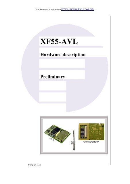
GSM/GPRS and GPS device. Figure 1 shows the front and backside of the<br />
<strong>XF55</strong>-<strong>AVL</strong> module.<br />
a) top view b) bottom view<br />
Figure 1: Top and bottom view of <strong>XF55</strong>-<strong>AVL</strong> module<br />
The compact design of the <strong>XF55</strong>-<strong>AVL</strong> module makes it easy to integrate<br />
GSM/GPRS and GPS as an all-in-one solution. The <strong>XF55</strong>-<strong>AVL</strong> is designed for<br />
application that prefers to use board-to-board connection to the main PCB<br />
application platform. Due to its summit form factor it offers a highperformance<br />
combination between small form factor and improved flexibility<br />
for smaller and medium-sized projects. The combination of these two<br />
technologies in such a small form-factor device will make many new asset<br />
tracking applications possible, particularly in the fields of transportation,<br />
logistics and security. This combination concept builds perfect basis for the<br />
design tracking solutions for applications such as fleet management, vehicle<br />
tracking, navigation, emergency calling, location-based services and others. It<br />
saves significantly both time and cost for integration of additional hardware<br />
components.<br />
This confidential document is a property of FALCOM GmbH and may not be copied or circulated without previous permission.<br />
Page 6
<strong>XF55</strong>-<strong>AVL</strong> HARDWARE DESCRIPTION VERSION 0.01<br />
The integrated GPS module provides more then enough precise location<br />
information using satellite signals to enable users to determine where they are<br />
anywhere in the world. The <strong>XF55</strong>-<strong>AVL</strong> module has also an integrated TCXO<br />
that allows the support for high sensitivity SiRFXTrac2 software.<br />
An integrated Combo-Memory into the <strong>XF55</strong>-<strong>AVL</strong> module of GPS part,<br />
combination Flash and SRAM is high-performance memory solution that<br />
significantly improves the system performance. It saves the <strong>XF55</strong>-<strong>AVL</strong><br />
software in its flash memory section and static RAM section provides the<br />
additional storage capacity.<br />
A compact “stacked FLASH/SRAM” device stores the <strong>XF55</strong>-<strong>AVL</strong> software in<br />
the flash memory section of GSM/GPRS part, and static RAM section provides<br />
the additional storage capacity required by GPRS connectivity.<br />
The physical interface to the module application is made through board-toboard<br />
connector. This is required for controlling the unit, receiving GPS<br />
location data, transferring data and audio signals and providing power supply<br />
lines. <strong>XF55</strong>-<strong>AVL</strong> provides two serial GSM interfaces (ASC0-provided on the<br />
80-pin connector and ASC1 provided on the 50-pin connector) and two serial<br />
GPS interfaces (Serial data 1 and Serial data 2) giving you maximum flexibility<br />
for easy integration with the Man-Machine Interface (MMI). For battery<br />
powered applications, <strong>XF55</strong>-<strong>AVL</strong> features a charging control which can be<br />
used to charge a Li-Ion battery. The charging circuit must be implemented<br />
external the module on your application platform.<br />
0.2 Circuit concept<br />
The <strong>XF55</strong>-<strong>AVL</strong> architecture includes the following major functional components<br />
(see figure 2):<br />
� Architecture integrates:<br />
� high-performance Tri Band GSM/GPRS core (operating at 26MHz)<br />
� 12 parallel channel low-power GPS core (operating at L1 1575.42<br />
MHz and C/A code 1,023 MHz chip rate)<br />
� ARM7TDMI Processor (at speed 25MHz) that controls all<br />
functions of the system<br />
� Power Control circuitry<br />
� 2 x Audio channels<br />
� Interface circuitry<br />
� Combo-Memory (2MB - 512KB) for loading software.<br />
� Physical interfaces:<br />
� 80-pin board-to-board connector (Type Hirose DF12C) serves as<br />
physical interface to the host application.<br />
� 50-pin board-to-board connector (Type Hirose DF12C) serves as<br />
physical interface for GSM/GPRS part to the host application.<br />
� provided pins for an external SIM card reader.<br />
� an ultra-miniature SMT GSM/GPRS antenna connector (Type<br />
U.FL-R-SMT) supplied from Hirose Ltd.<br />
This confidential document is a property of FALCOM GmbH and may not be copied or circulated without previous permission.<br />
Page 7
<strong>XF55</strong>-<strong>AVL</strong> HARDWARE DESCRIPTION VERSION 0.01<br />
� an ultra-miniature SMT GPS antenna connector (Type U.FL-R-<br />
SMT) supplied from Hirose Ltd.<br />
Figure 2: Architecture of the <strong>XF55</strong>-<strong>AVL</strong> module<br />
Please note that the GPS part of <strong>XF55</strong>-<strong>AVL</strong> operates with SiRF GSW2,<br />
version 2.32. There is no <strong>AVL</strong> software included in the delivery pack.<br />
Figure 3: Architecture of the <strong>XF55</strong>-<strong>AVL</strong> module operating with <strong>AVL</strong> or TCP/IP<br />
software application (optional)<br />
This confidential document is a property of FALCOM GmbH and may not be copied or circulated without previous permission.<br />
Page 8
<strong>XF55</strong>-<strong>AVL</strong> HARDWARE DESCRIPTION VERSION 0.01<br />
0.3 Used abbreviations<br />
Abbreviation Description<br />
AD Analog/Digita<br />
ADC Analog-to-Digital Converter<br />
AFC Automatic Frequency Control<br />
AGC Automatic Gain Control<br />
AMP Advanced Power Management<br />
ANSI American National Standards Institute<br />
ARFCN Absolute Radio Frequency Channel Number<br />
ARP Antenna Reference Point<br />
ASC0/ASC1 Asynchronous Controller. Abbreviations used for first and second<br />
serial interface of <strong>XF55</strong>-<strong>AVL</strong><br />
ASIC Application Specific Integrated Circuit<br />
B Thermistor Constant<br />
B2B Board-to-board connector<br />
BER Bit Error Rate<br />
BTS Base Transceiver Station<br />
CB or CBM Cell Broadcast Message<br />
CE Conformité Européene (European Conformity)<br />
CHAP Challenge Handshake Authentication Protocol<br />
CPU Central Processing Unit<br />
CS Coding Scheme<br />
CSD Circuit Switched Data<br />
CTS Clear to Send<br />
DAC Digital-to-Analog Converter<br />
DAI Digital Audio Interface<br />
dBW Decibel per Watt<br />
dBm0 Digital level, 3.14 dBm0 corresponds to full scale, see ITU G.711,<br />
A-law<br />
DCE Data Communication Equipment (typically modems, e.g. <strong>XF55</strong>-<br />
<strong>AVL</strong> GSM engine)<br />
DCS 1800 Digital Cellular System, also referred to as PCN<br />
DGPS Differential GPS<br />
DOP Dilution of Precision<br />
DRX Discontinuous Reception<br />
DSP Digital Signal Processor<br />
DSR Data Set Ready<br />
DTE Data Terminal Equipment (typically computer, terminal, printer or,<br />
for example, GSM application)<br />
DTR Data Terminal Ready<br />
DTX Discontinuous Transmission<br />
EFR Enhanced Full Rate<br />
EGSM Enhanced GSM<br />
EMC Electromagnetic Compatibility<br />
ESD Electrostatic Discharge<br />
ETS European Telecommunication Standard<br />
FCC Federal Communications Commission (U.S.)<br />
FDMA Frequency Division Multiple Access<br />
This confidential document is a property of FALCOM GmbH and may not be copied or circulated without previous permission.<br />
Page 9
<strong>XF55</strong>-<strong>AVL</strong> HARDWARE DESCRIPTION VERSION 0.01<br />
Abbreviation Description<br />
FR Full Rate<br />
GGA GPS Fixed Data<br />
GMSK Gaussian Minimum Shift Keying<br />
GPRS General Packet Radio Service<br />
GPS Global Positioning System<br />
GSM Global Standard for Mobile Communications<br />
HiZ High Impedance<br />
HR Half Rate<br />
I/O Input/Output<br />
IC Integrated Circuit<br />
IF Intermediate Frequency<br />
IMEI International Mobile Equipment Identity<br />
ISO International Standards Organization<br />
ITU International Telecommunications Union<br />
kbps kbits per second<br />
LED Light Emitting Diode<br />
Li-Ion Lithium-Ion<br />
LNA Low Noise Amplifier<br />
Mbps Mbits per second<br />
MMI Man Machine Interface<br />
MO Mobile Originated<br />
MS Mobile Station (GSM engine), also referred to as TE<br />
MSISDN Mobile Station International ISDN number<br />
MSK Minimum Shift Key<br />
MT Mobile Terminated<br />
NTC Negative Temperature Coefficient<br />
NMEA National Maritime Electronics Association<br />
OEM Original Equipment Manufacturer<br />
PA Power Amplifier<br />
PAP Password Authentication Protocol<br />
PBCCH Packet Switched Broadcast Control Channel<br />
PCB Printed Circuit Board<br />
PCL Power Control Level<br />
PCM Pulse Code Modulation<br />
PCN Personal Communications Network, also referred to as DCS 1800<br />
PCS Personal Communication System, also referred to as GSM 1900<br />
PDU Protocol Data Unit<br />
PLL Phase Locked Loop<br />
PPP Point-to-point protocol<br />
PRN Pseudo-Random Noise Number. The identity of GPS satellites<br />
PSU Power Supply Unit<br />
R&TTE Radio and Telecommunication Terminal Equipment<br />
RAM Random Access Memory<br />
RF Radio Frequency<br />
RMS Root Mean Square (value)<br />
ROM Read-only Memory<br />
RP Receive Protocol<br />
RTC Real Time Clock<br />
This confidential document is a property of FALCOM GmbH and may not be copied or circulated without previous permission.<br />
Page 10
<strong>XF55</strong>-<strong>AVL</strong> HARDWARE DESCRIPTION VERSION 0.01<br />
Abbreviation Description<br />
RTCM Radio Technical Commission for Maritime Services<br />
Rx Receive Direction<br />
SA Selective Availability<br />
SAR Specific Absorption Rate<br />
SELV Safety Extra Low Voltage<br />
SIM Subscriber Identification Module<br />
SMS Short Message Service<br />
SRAM Static Random Access Memory<br />
TA Terminal adapter (e.g. GSM engine)<br />
TDMA Time Division Multiple Access<br />
TE Terminal Equipment, also referred to as DTE<br />
Tx Transmit Direction<br />
UART Universal asynchronous receiver-transmitter<br />
URC Unsolicited Result Code<br />
USSD Unstructured Supplementary Service Data<br />
VSWR Voltage Standing Wave Ratio<br />
WAAS Wide Area Augmentation System<br />
FD SIM fix dialing phonebook<br />
LD SIM last dialing phonebook (list of numbers most recently dialed)<br />
MC Mobile Equipment list of unanswered MT calls (missed calls)<br />
ME Mobile Equipment phonebook<br />
ON Own numbers (MSISDNs) stored on SIM or ME<br />
RC Mobile Equipment list of received calls<br />
SM SIM phonebook<br />
Table 1: Used abbreviations<br />
0.4 Related documents<br />
1. ETSI GSM 07.05: “Use of Data Terminal Equipment–Data Circuit<br />
terminating Equipment interface for Short Message Service and Cell<br />
Broadcast Service”<br />
2. ETSI GSM 07.07 “AT command set for GSM Mobile Equipment”<br />
3. ITU-T V.25ter “Serial asynchronous automatic dialling and control”<br />
4. xf55_at_command_set.pdf<br />
5. gprs_startup_user_guide.pdf<br />
6. SiRF binary and NMEA protocol specification;<br />
www.falcom.de/download/manuals/SiRF<br />
7. xf55-avl_using_stepp_II_1.6.2_sw.pdf<br />
8. xf55_avl_tcp_ip_software_manual.pdf<br />
9. Multiplexer User's Guide (in preparation)<br />
10. Application Note 14: Audio and Battery Parameter Download (in<br />
preparation)<br />
11. Application Note 02: Audio Interface Design (in preparation)<br />
12. falcom_eCos_SDK_user_guide.pdf<br />
13. universal_evaluation_board_manual.pdf<br />
14. xf55_avl_getting_started.pdf<br />
15. xf55_avl_using_V2.0RC1_sw.pdf<br />
16. Application Note 01: Interrupt control<br />
This confidential document is a property of FALCOM GmbH and may not be copied or circulated without previous permission.<br />
Page 11
<strong>XF55</strong>-<strong>AVL</strong> HARDWARE DESCRIPTION VERSION 0.01<br />
1 Security<br />
IMPORTANT FOR THE EFFICIENT AND SAFE OPERATION OF YOUR<br />
GSM-MODEM, READ THIS INFORMATION BEFORE USE!<br />
Your cellular engine <strong>XF55</strong>-<strong>AVL</strong> is one of the most exciting and innovative<br />
electronic products ever developed. With it you can stay in contact with your<br />
office, your home, emergency services and others, wherever service is<br />
provided.<br />
This chapter contains important information for the safe and reliable use of the<br />
<strong>XF55</strong>-<strong>AVL</strong> module. Please read this chapter carefully before starting to use the<br />
cellular engine <strong>XF55</strong>-<strong>AVL</strong>.<br />
1.1 General information<br />
Your <strong>XF55</strong>-<strong>AVL</strong> device utilize the GSM/GPS standard for cellular technology.<br />
GSM is a newer radio frequency („RF“) technology than the current FM<br />
technology that has been used for radio communications for decades. The GSM<br />
standard has been established for use in the European community and<br />
elsewhere. Your <strong>XF55</strong>-<strong>AVL</strong> is actually a low power radio transmitter and<br />
receiver. It sends out and receives radio frequency energy. When you use your<br />
modem, the cellular system handling your calls controls both the radio<br />
frequency and the power level of your cellular modem.<br />
1.2 Exposure to RF energy<br />
There has been some public concern about possible health effects of using<br />
GSM modem. Although research on health effects from RF energy has focused<br />
for many years on the current RF technology, scientists have begun research<br />
regarding newer radio technologies, such as GSM. After existing research had<br />
been reviewed, and after compliance to all applicable safety standards had been<br />
tested, it has been concluded that the product is fit for use.<br />
If you are concerned about exposure to RF energy there are things you can do<br />
to minimize exposure. Obviously, limiting the duration of your calls will<br />
reduce your exposure to RF energy. In addition, you can reduce RF exposure<br />
by operating your cellular modem efficiently by following the guidelines<br />
below.<br />
1.3 Efficient modem operation<br />
In order to operate your modem at the lowest power level, consistent with<br />
satisfactory call quality please take note of the following hints.<br />
� If your modem has an extendible antenna, extend it fully. Some models<br />
allow you to place a call with the antenna retracted. However, your modem<br />
operates more efficiently with the antenna fully extended.<br />
� Do not hold the antenna when the modem is „IN USE“. Holding the<br />
antenna affects call quality and may cause the modem to operate at a<br />
higher power level than needed.<br />
This confidential document is a property of FALCOM GmbH and may not be copied or circulated without previous permission.<br />
Page 12
<strong>XF55</strong>-<strong>AVL</strong> HARDWARE DESCRIPTION VERSION 0.01<br />
1.4 Antenna care and replacement<br />
Do not use the modem with a damaged antenna. If a damaged antenna comes<br />
into contact with the skin, a minor burn may result. Replace a damaged antenna<br />
immediately. Consult your manual to see if you may change the antenna<br />
yourself. If so, use only a manufacturer antenna. Otherwise, have your antenna<br />
repaired by a qualified technician.<br />
Use only the supplied (if there is one) or approved antenna. Unauthorized<br />
antennas, modifications or attachments could damage the modem and may<br />
contravene local RF emission regulations.<br />
1.5 Driving<br />
Check the laws and regulations on the use of cellular devices in the area where<br />
you drive. Always obey them. Also, when using your modem while driving,<br />
please pay full attention to driving, pull off the road and park before making or<br />
answering a call if driving conditions so require. When applications are<br />
prepared for mobile use they should fulfil road-safety instructions of the<br />
current law!<br />
1.6 Electronic devices<br />
Most electronic equipment, for example in hospitals and motor vehicles is<br />
shielded from RF energy. However, RF energy may affect some<br />
malfunctioning or improperly shielded electronic equipment.<br />
1.7 Vehicle electronic equipment<br />
Check your vehicle manufacturer’s representative to determine if any on board<br />
electronic equipment is adequately shielded from RF energy.<br />
1.8 Medical electronic equipment<br />
Consult the manufacturer of any personal medical devices (such as<br />
pacemakers, hearing aids, etc.) to determine if they are adequately shielded<br />
from external RF energy.<br />
Turn your <strong>XF55</strong>-<strong>AVL</strong> device OFF in health care facilities when any<br />
regulations posted in the area instruct you to do so. Hospitals or health care<br />
facilities may be using RF monitoring equipment.<br />
1.9 Aircraft<br />
Turn your <strong>XF55</strong>-<strong>AVL</strong> OFF before boarding any aircraft.<br />
Use it on the ground only with crew permission.<br />
Do not use it in the air.<br />
To prevent possible interference with aircraft systems, Federal Aviation<br />
Administration (FAA) regulations require you to have permission from a crew<br />
member to use your modem while the plane is on the ground. To prevent<br />
interference with cellular systems, local RF regulations prohibit using your<br />
modem whilst airborne.<br />
This confidential document is a property of FALCOM GmbH and may not be copied or circulated without previous permission.<br />
Page 13
<strong>XF55</strong>-<strong>AVL</strong> HARDWARE DESCRIPTION VERSION 0.01<br />
1.10 Children<br />
Do not allow children to play with your <strong>XF55</strong>-<strong>AVL</strong> device. It is not a toy.<br />
Children could hurt themselves or others (by poking themselves or others in the<br />
eye with the antenna, for example). Children could damage the modem or<br />
make calls that increase your modem bills.<br />
1.11 Blasting areas<br />
To avoid interfering with blasting operations, turn your unit OFF when in a<br />
“blasting area” or in areas posted: „turn off two-way radio“. Construction crew<br />
often uses remote control RF devices to set off explosives.<br />
1.12 Potentially explosive atmospheres<br />
Turn your <strong>XF55</strong>-<strong>AVL</strong> device OFF when in any area with a potentially<br />
explosive atmosphere. It is rare, but your modems or their accessories could<br />
generate sparks. Sparks in such areas could cause an explosion or fire resulting<br />
in bodily injury or even death.<br />
Areas with a potentially explosive atmosphere are often, but not always, clearly<br />
marked. They include fuelling areas such as petrol stations; below decks on<br />
boats; fuel or chemical transfer or storage facilities; and areas where the air<br />
contains chemicals or particles, such as grain, dust or metal powders.<br />
Do not transport or store flammable gas, liquid or explosives, in the<br />
compartment of your vehicle which contains your modem or accessories.<br />
Before using your modem in a vehicle powered by liquefied petroleum gas<br />
(such as propane or butane) ensure that the vehicle complies with the relevant<br />
fire and safety regulations of the country in which the vehicle is to be used.<br />
1.13 Non-ionizing radiation<br />
As with other mobile radio transmitting equipment users are advised that for<br />
satisfactory operation and for the safety of personnel, it is recommended that<br />
no part of the human body be allowed to come too close to the antenna during<br />
operation of the equipment.<br />
The radio equipment shall be connected to the antenna via a non-radiating 50<br />
Ohm coaxial cable.<br />
The antenna shall be mounted in such a position that no part of the human body<br />
will normally rest close to any part of the antenna. It is also recommended to<br />
use the equipment not close to medical devices as for example hearing aids and<br />
pacemakers.<br />
This confidential document is a property of FALCOM GmbH and may not be copied or circulated without previous permission.<br />
Page 14
<strong>XF55</strong>-<strong>AVL</strong> HARDWARE DESCRIPTION VERSION 0.01<br />
2 Safety standards<br />
Your GSM/GPS module complies with all applicable RF safety standards.<br />
The embedded GMS/GPS module meet the safety standards for RF receivers<br />
and the standards and recommendations for the protection of public exposure<br />
to RF electromagnetic energy established by government bodies and<br />
professional organizations, such as directives of the European Community,<br />
Directorate General V in matters of radio frequency electromagnetic energy.<br />
This confidential document is a property of FALCOM GmbH and may not be copied or circulated without previous permission.<br />
Page 15
<strong>XF55</strong>-<strong>AVL</strong> HARDWARE DESCRIPTION VERSION 0.01<br />
3 Technical data<br />
3.1 General specifications of module <strong>XF55</strong>-<strong>AVL</strong><br />
� Power supply:<br />
� Power saving (GSM):<br />
� Power saving (GPS)<br />
� Charging<br />
� Temperature range:<br />
� Evaluation kit<br />
� Physical characteristics:<br />
� Firmware upgrade<br />
3.1.1 Power consumption<br />
� Supply voltage 3.3 V...4.8 V for the GSM/GPRS<br />
module<br />
� Separate power supply source: 3.3 V ± 5 % for<br />
the GPS device<br />
� Minimizes power consumption in SLEEP mode<br />
to 3 mA<br />
� TricklePower mode reduces power to
<strong>XF55</strong>-<strong>AVL</strong> HARDWARE DESCRIPTION VERSION 0.01<br />
GSM<br />
GPRS<br />
Peak supply<br />
current.<br />
Supply voltage 3.14 3.3 3.46 V<br />
Antenna<br />
voltage<br />
2.32 firmware<br />
XTrac firmware<br />
Average supply current<br />
50 100 µA POWER DOWN mode<br />
3 mA SLEEP mode @ DRX = 6<br />
MODE BAND<br />
15 mA IDLE mode EGSM 900<br />
15 GSM 1800/1900<br />
260 EGSM 900 *)<br />
180<br />
mA TALK mode<br />
GSM 1800/1900 **)<br />
15<br />
15<br />
mA IDLE GPRS<br />
EGSM 900<br />
GSM 1800/1900<br />
300 EGSM 900 *)<br />
230<br />
mA<br />
DATA mode GPRS,<br />
(4 Rx, 1 Tx) GSM 1800/1900 **)<br />
450 EGSM 900 *)<br />
320<br />
mA<br />
DATA mode GPRS,<br />
(3 Rx, 2 Tx) GSM 1800/1900 **)<br />
1.6 A<br />
Power control level *)<br />
During transmission slot every 4.6 ms.<br />
60 74<br />
0.65 13 69<br />
0.65 69<br />
71 84<br />
68 88<br />
3 V<br />
GPS engine<br />
mA<br />
mA<br />
Voltage must stay within the min/max<br />
values, including voltage drop, ripple, and<br />
spikes.<br />
Table 2: Power consumption of GSM/GPRS and GPS parts<br />
________________________________________________<br />
*) in transmit/receive mode at maximum power level (5)<br />
**) in transmit/receive mode at maximum power level (0)<br />
***) Time between fixes<br />
GPS_VCC_RF pin connected to<br />
GPS_VANT pin. The current<br />
consumption of connected active GPS is 3<br />
mA.<br />
Power mode <strong>description</strong><br />
During signal receiving in continuous<br />
mode (GPS fix is already obtained)<br />
During signal receiving in TricklePower<br />
mode (GPS fix is obtained)<br />
TricklePower Mode settings:<br />
Total period = 2000 ms<br />
Tracking State = 240 ms<br />
CPU mode = 630 ms<br />
Trickle State = 1130 ms<br />
During signal receiving in Push-To-Fix<br />
mode (GPS fix is already obtained)<br />
During signal receiving in continuous<br />
mode (GPS fix is already obtained)<br />
During signal receiving in APM mode<br />
APM Mode settings:<br />
AMP enable = True<br />
Num AMP cycle before sleep = 0<br />
Time between fixes = 30 sec<br />
Power Duty cycle = 50 %<br />
Timing priority preference = Tbf ***)<br />
Accuracy Priority preference = no preference<br />
This confidential document is a property of FALCOM GmbH and may not be copied or circulated without previous permission.<br />
Page 17
<strong>XF55</strong>-<strong>AVL</strong> HARDWARE DESCRIPTION VERSION 0.01<br />
3.2 Technical specifications of GSM/GPRS engine<br />
� Frequency bands:<br />
� GSM class:<br />
� Transmit power:<br />
� GPRS connectivity:<br />
� DATA:<br />
� SMS:<br />
� MMS:<br />
GPRS ⇒<br />
CSD ⇒<br />
WAP ⇒<br />
� Tri band: EGSM 900, GSM 1800, GSM 1900<br />
� Compliant to GSM Phase 2/2+<br />
� Small MS<br />
� Class 4 (2 W) at EGSM900<br />
� Class 1 (1 W) at GSM1800 and GSM 1900<br />
� GPRS multi-slot class 10<br />
� GPRS mobile station class B<br />
� GPRS data downlink transfer: max. 85.6 kbps<br />
(see table 3).<br />
� GPRS data uplink transfer: max. 42.8 kbps (see<br />
table 3).<br />
� Coding scheme: CS-1, CS-2, CS-3 and CS-4.<br />
� <strong>XF55</strong>-<strong>AVL</strong> supports two protocols PAP<br />
(Password Authentication Protocol) and CHAP<br />
(Challenge Handshake Authentication Protocol)<br />
commonly used for PPP connections.<br />
� Supports of Packet Switched Broadcast Control<br />
Channel (PBCCH) allows you to benefit from<br />
enhanced GPRS performance when offered by<br />
the network operators.<br />
� CSD transmission rates: 2.4, 4.8, 9.6, 14.4 kbps,<br />
non-transparent, V.110.<br />
� Unstructured Supplementary Services Data<br />
(USSD) support.<br />
� WAP compliant.<br />
� MT, MO, CB, Text and PDU mode<br />
� SMS storage: SIM card plus 25 SMS locations in<br />
the mobile equipment<br />
� Transmission of SMS alternatively over CSD or<br />
GPRS. Preferred mode can be user-defined.<br />
� MMS compliant<br />
This confidential document is a property of FALCOM GmbH and may not be copied or circulated without previous permission.<br />
Page 18
<strong>XF55</strong>-<strong>AVL</strong> HARDWARE DESCRIPTION VERSION 0.01<br />
� FAX:<br />
� SIM interface:<br />
� Casing:<br />
� Temperature control<br />
and auto switch-off:<br />
� External antenna:<br />
� Audio interfaces:<br />
� Audio features:<br />
� Group 3: class 1, class 2<br />
� Supported SIM card: 3 V<br />
� External SIM card reader has to be connected<br />
via interface connector (note that card reader is<br />
not part of module <strong>XF55</strong>-<strong>AVL</strong>)<br />
� Fully shield<br />
� Two serial interfaces (ASC0, ASC1):<br />
� Constant temperature control prevents damage to<br />
module <strong>XF55</strong>-<strong>AVL</strong> when the specified<br />
temperature is exceeded. When an emergency<br />
call is in progress the automatic temperature<br />
shutdown functionality is deactivated. (see<br />
chapter 7.2 for further details)<br />
� Connected via 50 Ohm antenna connector or<br />
antenna pad.<br />
� Two analogue audio interfaces, one digital audio<br />
interface (DAI)<br />
Speech codec modes:<br />
� Half Rate (ETS 06.20)<br />
� Full Rate (ETS 06.10)<br />
� Enhanced Full Rate (ETS 06.50/06.60/06.80)<br />
� Adaptive Multi Rate (AMR)<br />
Handsfree operation<br />
� Echo cancellation<br />
� Noise reduction<br />
� 2.65V level, bi-directional bus for AT<br />
commands and data<br />
� ASC0↔full-featured 8-wire serial interface.<br />
Supports RTS0/CTS0 hardware handshake and<br />
software XON/XOFF flow control. Multiplex<br />
ability according to GSM 07.10 Multiplexer<br />
Protocol.<br />
� ASC1↔4-wire serial interface. Supports<br />
RTS1/CTS1 hardware handshake and software<br />
XON/XOFF flow control.<br />
� Baud rate: 300 bps ... 230 kbps on ASC0 and<br />
ASC1<br />
This confidential document is a property of FALCOM GmbH and may not be copied or circulated without previous permission.<br />
Page 19
<strong>XF55</strong>-<strong>AVL</strong> HARDWARE DESCRIPTION VERSION 0.01<br />
� Phonebook management:<br />
� SIM Application Toolkit:<br />
� Ringing tones:<br />
� Real time clock:<br />
� Timer function:<br />
� Internal memory:<br />
� Support of TTY/CTM:<br />
� Autobauding (on ASC0 only) detects 1200,<br />
2400, 4800, 9600, 19200, 38400, 57600, 115200,<br />
230400 bps<br />
� Supported phonebook types: SM, FD, LD, MC,<br />
RC, ON, ME<br />
� Supports SAT class 3, GSM 11.14 Release 98<br />
� Offers a choice of 7 different ringing<br />
tones/melodies, easily selectable with AT<br />
command<br />
� Implemented<br />
� Programmable via AT command<br />
� Stacked Flash/SRAM<br />
� To benefit from TTY communication via GSM,<br />
CTM equipment can be connected to one of the<br />
three audio interfaces.<br />
Coding scheme 1 Timeslot 2 Timeslots 4 Timeslots<br />
CS-1: 9.05 kbps 18.1 kbps 36.2 kbps<br />
CS-2: 13.4 kbps 26.8 kbps 53.6 kbps<br />
CS-3: 15.6 kbps 31.2 kbps 62.4 kbps<br />
CS-4: 21.4 kbps 42.8 kbps 85.6 kbps<br />
Table 3: Coding schemes and maximum net data rates over air interface<br />
Please note that the values listed above are the maximum ratings which, in practice, are<br />
influenced by a great variety of factors, primarily, for example, traffic variations and network<br />
coverage.<br />
3.3 Technical specifications of GPS receiver<br />
� GPS features:<br />
� Accuracy:<br />
� OEM single board 12 channel GPS receiver, L1<br />
1575.42 MHz, C/A code 1,023 MHz chip rate.<br />
� GPS receiver with SiRFstarIIe/LP chip set<br />
� Processor type ARM7/TDMI<br />
� SiRF GSW2, version 2.32<br />
� Position 10 meters CEP without SA.<br />
This confidential document is a property of FALCOM GmbH and may not be copied or circulated without previous permission.<br />
Page 20
<strong>XF55</strong>-<strong>AVL</strong> HARDWARE DESCRIPTION VERSION 0.01<br />
� DGPS Accuracy:<br />
� Datum:<br />
� Sensitivity*:<br />
� Velocity 0.1 meters/second, without SA<br />
� Time 1 microsecond synchronized to GPS time<br />
� Position 1 to 5 meters, typical.<br />
� Velocity 0.05 meters/second, typical<br />
� WGS-84.<br />
� Tracking 16 dBHz.<br />
� Hot Start 23 dBHz<br />
� Warm Start 28 dBHz<br />
� Cold Start 32 dBHz<br />
• The sensitivity value is specified at the correlator. On a GPS Evaluation Receiver<br />
using SiRFXTrac2 firmware with the supplied antenna, 32 dBHz is equivalent to<br />
-142 dBm or -172 dBW. Other board and antenna characteristics will vary.<br />
� Acquisition Rate:<br />
� Dynamic Conditions:<br />
� Backup battery power:<br />
� Casing:<br />
� Time – 1 PPS Pulse:<br />
� Supported protocols:<br />
� Cold start
<strong>XF55</strong>-<strong>AVL</strong> HARDWARE DESCRIPTION VERSION 0.01<br />
� Crystal oscillator (TCXO) specification:<br />
� Baud rate: 4800 bps on the GPS_SD1 port, 9600<br />
bps on the GPS_SD2 port (see chapter 11.5.1.1<br />
for SiRFXTrac2 software settings).<br />
� 8 data bits, no parity, 1 stop bit<br />
Typical phase noise density 1 Hz offset -57.0 dBc/Hz<br />
Typical phase noise density 10 Hz offset -88.0 dBc/Hz<br />
Typical phase noise density 100 Hz offset -112.0 dBc/Hz<br />
Typical phase noise density 1 kHz offset -130.0 dBc/Hz<br />
Typical phase noise density 10 kHz offset -140.0 dBc/Hz<br />
Load sensitivity ± 10 % load change 0.2 ± ppm<br />
Long term stability Frequency drift over 1 year 0.5 to 2.0 ± ppm<br />
� External antenna:<br />
� Memory:<br />
� Separate GPS antenna connector. See figure 37<br />
for details<br />
� Combo-Memory (2 MB Flash–512 KB SRAM)<br />
� Additional software options (can be obtained separately):<br />
� <strong>AVL</strong>: The integration of <strong>AVL</strong> software into the<br />
on-board Memory allows the module <strong>XF55</strong>-<br />
<strong>AVL</strong> a wide range of tracking solutions in<br />
applications that can locally and remotely be<br />
configured. The concept of the device is based<br />
on a simple implementation for a wide range of<br />
applications with low costs and high flexibility<br />
(see related documents [7 and 15])<br />
� TCP/IP: The integration of TCP/IP stack into the<br />
<strong>XF55</strong>-<strong>AVL</strong> converts it to a stand-alone client<br />
that can be connected to the internet through any<br />
GSM 900/1800/1900 network. The module can<br />
also send and receive data by GSM and GPRS<br />
network using TCP/IP stack. It supports SMS,<br />
DATA and FAX calls. The <strong>XF55</strong>-<strong>AVL</strong> using<br />
module TCP/IP can be easily controlled by using<br />
AT or IP commands (see related document [8])<br />
� SiRFXTrac2 (high sensitivity stand alone<br />
software) see section 11.5.1<br />
This confidential document is a property of FALCOM GmbH and may not be copied or circulated without previous permission.<br />
Page 22
<strong>XF55</strong>-<strong>AVL</strong> HARDWARE DESCRIPTION VERSION 0.01<br />
4 GSM/GPRS application interface<br />
4.1 Description of operating modes<br />
The chapter below briefly summarizes the various operating modes referred to<br />
in the following chapters. GPS operating modes are also described in chapter<br />
5.2.<br />
Definition of the GPRS class B mode of operation:<br />
The definition of GPRS class B mode is, the MS can be attached to both<br />
GPRS and other GSM services, but the MS can only operate one set of<br />
services at a time. Class B enables making or receiving a voice call, or<br />
sending/receiving an SMS during a GPRS connection. During voice calls or<br />
SMS, GPRS services are suspended and then resumed automatically after the<br />
call or SMS session has ended.<br />
4.1.1 Normal mode operation<br />
4.1.1.1 GSM/GPRS SLEEP<br />
Various power save modes set with AT+CFUN command. Software is active to<br />
minimum extent. If the module was registered to the GSM network in IDLE<br />
mode, it is registered and paging with the BTS in SLEEP mode, too. Power<br />
saving can be chosen at different levels: The NON-CYCLIC SLEEP mode<br />
(AT+CFUN=0) disables the AT interface. The CYCLIC SLEEP modes<br />
AT+CFUN=5,6,7,8 and 9 alternatively activate and deactivate the AT<br />
interfaces to allow permanent access to all AT commands.<br />
4.1.1.2 GSM IDLE<br />
Software is active. Once registered to the GSM network, paging with BTS is<br />
carried out. The module is ready to send and receive.<br />
4.1.1.3 GSM TALK<br />
Connection between two subscribers is in progress. Power consumption<br />
depends on network coverage individual settings, such as DTX off/on,<br />
FR/EFR/HR, hopping sequences, antenna.<br />
4.1.1.4 GPRS IDLE<br />
Module is ready for GPRS data transfer, but no data is currently sent or<br />
received. Power consumption depends on network settings and GPRS<br />
configuration (e.g. multislot settings).<br />
This confidential document is a property of FALCOM GmbH and may not be copied or circulated without previous permission.<br />
Page 23
<strong>XF55</strong>-<strong>AVL</strong> HARDWARE DESCRIPTION VERSION 0.01<br />
4.1.1.5 GPRS DATA<br />
GPRS data transfer in progress. Power consumption depends on network<br />
settings (e.g. power control level), uplink/downlink data rates and GPRS<br />
configuration (e.g. used multislot settings).<br />
4.1.2 Power down<br />
Normal shutdown after sending the AT^SMSO command. The Power Supply<br />
ASIC (PSU-ASIC) disconnects the supply voltage from the base band part of<br />
the circuit. Only a voltage regulator in the PSU-ASIC is active for powering<br />
the RTC. Software is not active. The serial interfaces are not accessible.<br />
Operating voltage (connected to GSM_BATT+) remains applied.<br />
4.1.3 Alarm mode<br />
Alarm mode restricted operation launched by RTC alert function while the<br />
module is in POWER DOWN mode. Module will not be registered to GSM<br />
network. Limited number of AT commands is accessible.<br />
4.1.4 Charge-only mode<br />
Limited operation for battery powered applications. Enables charging while<br />
module is detached from GSM network. Limited number of AT commands is<br />
accessible. There are several ways to launch Charge-only mode:<br />
� From POWER DOWN mode: Connect charger to the charger input<br />
pin of the external charging circuit and the GSM_POWER pin of<br />
module when <strong>XF55</strong>-<strong>AVL</strong> was powered down by AT^SMSO.<br />
� From Normal mode: Connect charger to the charger input pin of the<br />
external charging circuit and the GSM_POWER pin of module, then<br />
enter AT^SMSO.<br />
4.1.5 Charge mode during normal operation<br />
Normal operation (SLEEP, IDLE, TALK, GPRS IDLE, and GPRS DATA) and<br />
charging are running in parallel. Charge mode changes to Charge-only mode<br />
when the module is powered down before charging has been completed.<br />
4.2 Description of the 80-pin double-row connector<br />
Please note that the reference voltages listed in table 4 are the values measured<br />
directly on the <strong>XF55</strong>-<strong>AVL</strong> module. They do not apply to the accessories<br />
connected. If an input pin is specified for VIHmax = 3.3V, be sure never to<br />
exceed the stated voltage. The value 3.3 V is an absolute maximum rating. The<br />
Hirose DF12C board-to-board connector on <strong>XF55</strong>-<strong>AVL</strong> is a 80-pin double-row<br />
receptacle. The names and the position of the pins can be seen from figure 4<br />
below which shows the top view of <strong>XF55</strong>-<strong>AVL</strong>.<br />
Please note that, both application interfaces (80- and 50-pin connectors) of the<br />
<strong>XF55</strong>-<strong>AVL</strong> module could not concurrently be used. The second application<br />
interface (ASC1) is not included on the 80-pin connector, it is available on the<br />
50-pin connector for user applications.<br />
This confidential document is a property of FALCOM GmbH and may not be copied or circulated without previous permission.<br />
Page 24
<strong>XF55</strong>-<strong>AVL</strong> HARDWARE DESCRIPTION VERSION 0.01<br />
Figure 4: Pin assignment on the 80-pin connector (bottom view on <strong>XF55</strong>-<strong>AVL</strong>)<br />
PIN NAME I/O DISCRIPTION LEVEL<br />
1 GPS_VANT I<br />
Power supply for an active<br />
antenna. See chapter 5.5<br />
Up to +12 V DC/max. 25 mA<br />
2 GPS_VCC_RF O<br />
Supply voltage of RF<br />
section. See chapter 5.5<br />
+ 3.0 V DC/max. 25 mA<br />
3<br />
4<br />
GPS_VCC<br />
GPS_VCC<br />
I<br />
Main power supply. See<br />
chapter 5.5<br />
+ 3.3 V DC ±5 %/max: 100 mA<br />
5 GSM_RXDDAI I<br />
VOLmax = 0.2 V at I = 1 mA<br />
6 GSM_TFSDAI O Digital audio interface VOHmin = 2.35 V at I = -1 mA<br />
7 GSM_SCLK I<br />
VOHmax = 2.73 V<br />
8 GSM_TXDDAI O If not used leave all pins<br />
open.<br />
VILmax = 0.5 V<br />
VIHmin = 1.95 V, VIHmax = 3.3 V<br />
9 GSM_RFSDAI I<br />
IImax = 330 µA at VIN = 3.3 V<br />
10 GPS_OUT_A1<br />
11 GPS_OUT_A2<br />
12 GPS_OUT_A3<br />
13 GPS_OUT_A4<br />
14 GPS_OUT_A5<br />
15 GPS_OUT_A6<br />
16 GPS_OUT_A7<br />
17 GPS_OUT_A8<br />
18 GPS_IN_1<br />
19 GPS_IN_2<br />
20 GPS_IN_3<br />
21 GPS_IN_4<br />
22 GPS_IN_5<br />
23 GPS_IN_6<br />
24 GPS_IN_7<br />
25 GPS_IN_8<br />
26 GPS_GPIO15<br />
27 GPS_GPIO10<br />
28 GPS_GPIO7<br />
29 GPS_GPIO6<br />
30 GPS_GPIO5<br />
31 GPS_GPIO1<br />
32 GPS_GPIO0<br />
33 GPS_SDI1<br />
O<br />
34 GPS_SDO1 O<br />
35 GPS_TMARK<br />
I<br />
General propose outputs<br />
See chapter 5.6.4<br />
General propose inputs<br />
See chapter 5.6.3<br />
Output 3.3 V DC/50 mA<br />
Are configured as active low level<br />
I/O See chapter 5.6.2 CMOS 3.3 V DC<br />
I Serial Data Input A (first<br />
receive line). See chapter<br />
5.6.1<br />
Serial Data Output A (first<br />
transmit line). See chapter<br />
5.6.1<br />
O 1 PPS Time Mark Output.<br />
See chapter 5.6<br />
CMOS 3.3V DC level<br />
CMOS 3.3V DC level<br />
CMOS 3.3 V DC<br />
This confidential document is a property of FALCOM GmbH and may not be copied or circulated without previous permission.<br />
Page 25
<strong>XF55</strong>-<strong>AVL</strong> HARDWARE DESCRIPTION VERSION 0.01<br />
36 GPS_BOOTSEL<br />
I Boots in update mode, if<br />
high. See chapter 5.6<br />
Control output for Trickle-<br />
CMOS 3.3 V DC<br />
37 GPS_RFPC1 O Power Mode.<br />
See chapter 5.6<br />
+ 2.85 V DC / max. 25 mA<br />
38 GPS_M-RST I<br />
Reset the unit if Active<br />
Low. See chapter 5.6<br />
Supply voltage, e.g. for an<br />
external LED or level<br />
shifter. The external digital<br />
CMOS<br />
39 GSM_VDD O<br />
logic must not cause any<br />
spikes or glitches on voltage<br />
VDD. Not available in<br />
POWER DOWN mode.<br />
VDD signalizes the “ON”<br />
state of the module.<br />
If unused keep it open.<br />
VDDmin = 2.84 V, VDDmax = 2.96 V<br />
Imax = -10 mA<br />
CLmax = 1 µF<br />
40 GSM_VDDLP I/O<br />
Supplies the RTC with<br />
power via an external<br />
capacitor or buffer battery<br />
if no VBATT+ is applied.<br />
If not used leave it open.<br />
RI =1 kΩ<br />
VOmax 4.0 V (output)<br />
VImin = 2.2 V, VImax = 5.5 V (input)<br />
IItyp = 10 µA at BATT+ = 0 V<br />
Mobile in POWER DOWN mode:<br />
VImin = 1.2V<br />
41 GSM_GND<br />
42<br />
43<br />
44<br />
GSM_GND<br />
GSM_GND<br />
GSM_GND<br />
-<br />
Negative operating voltage<br />
(grounds).<br />
0 V<br />
45 GSM_GND<br />
46 GSM_VBATT<br />
47 GSM_VBATT<br />
48 GSM_VBATT<br />
49 GSM_VBATT<br />
50 GSM_VBATT<br />
51 GSM_SYNC O<br />
52<br />
GSM_BATT_<br />
TEMP<br />
I<br />
I<br />
Power supply input. 5<br />
BATT+ pins to be<br />
connected in parallel. 5<br />
GND pins to be connected<br />
in parallel. The power<br />
supply must be able to meet<br />
the requirements of current<br />
consumption in a Tx burst<br />
(up to 3 A). Sending with<br />
two timeslots doubles the<br />
duration of current pulses<br />
to 1154 µs (every 4.616 ms)!<br />
These pins are also linked<br />
to the GPS part, which<br />
power the RTC and SRAM<br />
of GPS receiver.<br />
Indicates increased current<br />
consumption during uplink<br />
transmission burst. Note<br />
that timing is different<br />
during handover.<br />
Alternatively used to<br />
control status LED (see<br />
chapter 4.11.2.2).<br />
If not used leave it open.<br />
Input to measure the<br />
battery temperature over<br />
NTC resistor. NTC should<br />
be installed inside or near<br />
battery pack to enable the<br />
charging algorithm and<br />
deliver temperature values.<br />
VI = 3.3 V to 4.8 V<br />
VInorm = 4.1 V<br />
Imax < 2 A (during Tx burst)<br />
1 x Tx, peak current 577 µs every<br />
4.616 ms<br />
2 x Tx, peak current 1154 µs every<br />
4.616 ms<br />
VOLmax = 0.2 V at I = 1 mA<br />
VOHmin = 2.35 V at I = -1 mA<br />
VOHmax = 2.73 V<br />
1 Tx, 877 µs impulse each 4.616 ms<br />
and<br />
2 Tx, 1454 µs impulse each<br />
4.616 ms, with 300 µs forward time.<br />
Connect NTC with RNTC ≈ 10 kΩ @<br />
25 °C to ground.<br />
This confidential document is a property of FALCOM GmbH and may not be copied or circulated without previous permission.<br />
Page 26
<strong>XF55</strong>-<strong>AVL</strong> HARDWARE DESCRIPTION VERSION 0.01<br />
53 GSM_POWER I<br />
If not used leave it open.<br />
This line signals to the<br />
processor that the charger<br />
is connected.<br />
If not used leave it open<br />
This line is a current source<br />
VImin = 3.0 V<br />
VImax = 15 V<br />
54 GSM_CHARGE O<br />
for the charge FET with a<br />
10 kΩ resistance between<br />
gate and source.<br />
If not used leave it open.<br />
IGSM_CHARGE = -300 µA ... –600 µA<br />
@ 3 V < VGSM_CHARGE < VLOAD<br />
O Serial Data Output B CMOS 3.3 V DC level<br />
55 GPS_SDO2<br />
(second transmit line). See<br />
chapter 5.6.1<br />
I Serial Data Input B (second CMOS 3.3 V DC level<br />
56 GPS_SDI2<br />
receive line). See chapter<br />
5.6.1<br />
57<br />
58<br />
59<br />
60<br />
61<br />
62<br />
63<br />
64<br />
GSM_RXDO<br />
GSM_TXDO<br />
GSM_DSRO<br />
GSM_RINGO<br />
GSM_RTSO<br />
GSM_DTRO<br />
GSM_CTSO<br />
GSM_DCDO<br />
O<br />
I<br />
O<br />
O<br />
I<br />
I<br />
O<br />
O<br />
First serial interface<br />
(ASC0) for AT commands<br />
or data stream.<br />
To avoid floating if output<br />
pins are high-impedance,<br />
use pull-up resistors tied to<br />
GSM_VDD or pull-down<br />
resistors tied to GND. See<br />
chapter 4.3.3.1.<br />
If not used leave it open.<br />
This line must be driven by<br />
an Open Drain or Open<br />
Collector driver.<br />
Emergency shutdown<br />
VOLmax = 0.2 V at I = 1 mA<br />
VOHmin = 2.35 V at I = -1 mA<br />
VOHmax = 2.73 V<br />
VILmax = 0.5 V<br />
VIHmin = 1.95 V, VIHmax=3.3 V<br />
GSM_DTR0, GSM_RTS0: Imax =<br />
-90 µA at VIN = 0 V<br />
GSM_TXD0: Imax = -30 µA at<br />
VIN = 0 V<br />
deactivates the power RI 22 kΩ<br />
supply to the module. The VILmax = 0.5 V at Imax = -100 µA<br />
module can be reset if /IGT VOpenmax = 2.73 V<br />
is activated after emergency Signal<br />
65<br />
GSM_EMERG<br />
OFF<br />
I<br />
shutdown. To switch the<br />
mobile off use the<br />
AT^SMSO command.<br />
To avoid floating if pin is<br />
high impedance, use pulldown<br />
resistor tied to GND.<br />
See chapter 4.3.3.1.<br />
/EMERGOFF also indicates<br />
the internal watchdog<br />
function.<br />
If not used leave it open.<br />
~~~ |______| ~~~ Active Low ≥<br />
3.2 s<br />
Watchdog:<br />
VOLmax = 0.35 V at I = 10 µA<br />
VOHmin= 2.25 V at I = -10 µA<br />
fOmin = 0.16 Hz<br />
fOmax = 1.55 Hz<br />
66 GSM_IGT I<br />
Input to switch the mobile<br />
ON. The line must be<br />
driven low by an Open<br />
Drain or Open Collector<br />
driver.<br />
RI ≈ 100 kΩ, CI ≈1 nF<br />
VILmax = 0.5 V at Imax = -20 µA<br />
VOpenmax = 2.3 V<br />
ON ~~~ |____| ~~~ Active Low ≥100 ms<br />
67 GSM_CCGND - SIM interface<br />
0 V (Ground)<br />
RI ≈ 100 kΩ<br />
68 GSM_CCIN I<br />
GSM_CCIN = high, SIM<br />
card holder closed (no card<br />
VILmax = 0.5 V<br />
VIHmin = 2.15 V at I = 20 µA,<br />
recognition) Maximum VIHmax = 3.3 V at I = 30 µA<br />
cable length 200 mm to SIM RO ≈ 47 Ω<br />
69 GSM_CCRST O<br />
card holder.<br />
All signals of SIM interface<br />
VOLmax = 0.25 V at I = 1 mA<br />
VOHmin = 2.3 V at I = -1 mA<br />
are protected against ESD VOHmax = 2.73 V<br />
This confidential document is a property of FALCOM GmbH and may not be copied or circulated without previous permission.<br />
Page 27
<strong>XF55</strong>-<strong>AVL</strong> HARDWARE DESCRIPTION VERSION 0.01<br />
70 GSM_CCDATA I/O<br />
71 GSM_CCCLK O<br />
72 GSM_CCVCC O<br />
73 GSM_MICN1 I(-)<br />
74 GSM_MICP1 I(+)<br />
75 GSM_MICP2 I(+)<br />
76 GSM_MICN2 I(-)<br />
77 GSM_EPN1 O(-)<br />
78 GSM_EPP1 O(+)<br />
79 GSM_EPP2 O(+)<br />
80 GSM_EPN2 O(-)<br />
with a special diode array.<br />
Usage of GSM_CCGND is<br />
mandatory.<br />
Balanced microphone<br />
input. To be decoupled with<br />
2 capacitors (CK = 100 nF),<br />
if connected to a<br />
microphone or another<br />
device.<br />
If not used leave both pins<br />
open.<br />
Balanced microphone<br />
input. Can be used to<br />
directly feed an active<br />
microphone.<br />
If used for another signal<br />
source, e.g. op amp, to be<br />
decoupled with capacitors.<br />
If not used leave both pins<br />
open.<br />
Analog audio interfaces.<br />
Balanced audio output. Can<br />
be used to directly operate<br />
an earpiece.<br />
If not used leave both pins<br />
open.<br />
Analog audio interfaces.<br />
The audio output is<br />
balanced and can directly<br />
operate an earpiece.<br />
If not used leave both pins<br />
open.<br />
RI ≈ 10 kΩ<br />
VILmax = 0.5 V<br />
VIHmin = 1.95 V, VIHmax = 3.3 V<br />
RO ≈ 220 Ω<br />
VOLmax = 0.4 V at I = 1 mA<br />
VOHmin = 2.15 V at I = -1 mA<br />
VOHmin = 2.55 V at I = -20 µA<br />
VOHmax = 2.96 V<br />
RO ≈ 220 Ω<br />
VOLmax = 0.4 V at I = 1 mA<br />
VOHmin = 2.15 V at I = -1 mA<br />
VOHmax = 2.73 V<br />
ROmax = 5 Ω<br />
GSM_CCVCCmin = 2.84 V,<br />
GSM_CCVCCmax = 2.96 V<br />
Imax = -20 mA<br />
RI ≈ 50k Ω differential<br />
VImax = 1.03 Vpp<br />
See also Table 30.<br />
RI = 2 kΩ differential<br />
VImax = 1.03 Vpp<br />
See also Table 30.<br />
VOmax = 3.7 Vpp<br />
See also Table 29.<br />
VOmax = 3.7 Vpp<br />
See also Table 29.<br />
Table 4: Pin <strong>description</strong> of 80-pin board-to-board connector (primary application interface)<br />
______________________________________________________<br />
CMOS 3.3 V level:<br />
Input High = 2.0 - 3.3 V DC; I_leakage = 2 µA<br />
Input Low = 0 - 0.8 V DC, I_leakage = 2 µA<br />
Output High = min. 2.4 V DC, Ioh = 2 mA<br />
Output Low = max 0.4 V DC, Ioh = 2 mA<br />
4.3 Description of the 50-pin double-row connector<br />
The Hirose DF12C board-to-board connector on <strong>XF55</strong>-<strong>AVL</strong> is a 50-pin<br />
double-row receptacle. The names and the positions of the pins can be seen<br />
from figure 5 below which shows the top view of <strong>XF55</strong>-<strong>AVL</strong>.<br />
This confidential document is a property of FALCOM GmbH and may not be copied or circulated without previous permission.<br />
Page 28
<strong>XF55</strong>-<strong>AVL</strong> HARDWARE DESCRIPTION VERSION 0.01<br />
Please note that, both interfaces (80- and 50-pin connectors) could not<br />
concurrently be used. The second application interface (ASC1) included on this<br />
interface is not provided on the 80-pin connector. So, it is always usable for<br />
controlling the GSM/GPRS applications. In order to use it connect<br />
corresponded lines to the host interface.<br />
Figure 5: Pin assignment (top view on <strong>XF55</strong>-<strong>AVL</strong>)<br />
PIN NAME I/O DISCRIPTION LEVEL<br />
1 GSM_CCCLK O<br />
2 GSM_CCVCC O<br />
3 GSM_CCDATA I/O<br />
4 GSM_CCRST O<br />
5 GSM_CCIN I<br />
6 GSM_CCGND<br />
7 GSM_RXDDAI I<br />
8 GSM_TFSDAI O<br />
9 GSM_SCLK I<br />
10 GSM_TXDDAI O<br />
11 GSM_RFSDAI I<br />
12<br />
GSM_BATT_<br />
TEMP<br />
I<br />
SIM interface<br />
GSM_CCIN = high, SIM<br />
card holder closed (no card<br />
recognition) Maximum<br />
cable length 200 mm to SIM<br />
card holder.<br />
All signals of SIM interface<br />
are protected against ESD<br />
with a special diode array.<br />
Usage of GSM_CCGND is<br />
mandatory.<br />
Digital audio interface<br />
If unused keep all pins<br />
open.<br />
Input to measure the<br />
battery temperature over<br />
NTC resistor. NTC should<br />
be installed inside or near<br />
battery pack to enable the<br />
RO ≈ 220 Ω<br />
VOLmax = 0.4 V at I = 1 mA<br />
VOHmin = 2.15 V at I = -1 mA<br />
VOHmax = 2.73 V<br />
ROmax = 5 Ω<br />
GSM_CCVCCmin = 2.84 V,<br />
GSM_CCVCCmax = 2.96 V<br />
Imax = -20 mA<br />
RI ≈10 kΩ<br />
VILmax = 0.5 V<br />
VIHmin = 1.95 V, VIHmax=3.3 V<br />
RO ≈ 220 Ω<br />
VOLmax = 0.4 V at I = 1 mA<br />
VOHmin = 2.15 V at I = -1 mA<br />
VOHmin = 2.55 V at I = -20 µA<br />
VOHmax = 2.96 V<br />
RO ≈ 47 Ω<br />
VOLmax = 0.25 V at I = 1 mA<br />
VOHmin = 2.3 V at I = -1 mA<br />
VOHmax = 2.73 V<br />
RI ≈ 100 kΩ<br />
VILmax = 0.5 V<br />
VIHmin = 2.15 V at I = 20 µA,<br />
VIHmax = 3.3 V at I = 30 µA<br />
0 V (Ground)<br />
VOLmax = 0.2 V at I = 1 mA<br />
VOHmin = 2.35 V at I = -1 mA<br />
VOHmax = 2.73 V<br />
VILmax = 0.5 V<br />
VIHmin = 1.95 V, VIHmax=3.3 V<br />
IImax = 330 µA at VIN = 3.3 V<br />
Connect NTC with RNTC≈ 10 kΩ @<br />
25 °C to ground.<br />
This confidential document is a property of FALCOM GmbH and may not be copied or circulated without previous permission.<br />
Page 29
<strong>XF55</strong>-<strong>AVL</strong> HARDWARE DESCRIPTION VERSION 0.01<br />
13 GSM_SYNC O<br />
15 GSM_RXDO O<br />
17 GSM_TXDO I<br />
59 GSM_DSRO O<br />
32 GSM_RINGO O<br />
34 GSM_RTSO I<br />
35 GSM_DTRO I<br />
37 GSM_CTSO O<br />
39 GSM_DCDO O<br />
14 GSM_RXD1 O<br />
16 GSM_TXD1 I<br />
36 GSM_RTS1 I<br />
38 GSM_CTS1 O<br />
18 GSM_VDDLP I/O<br />
19 GSM_POWER I<br />
20 GSM_CHARGE O<br />
21 GSM_GND<br />
22 GSM_GND<br />
23 GSM_GND<br />
24 GSM_GND<br />
25 GSM_GND<br />
42 GSM_GND<br />
26 GSM_VBATT<br />
27 GSM_VBATT<br />
-<br />
I<br />
charging algorithm and<br />
deliver temperature values.<br />
If not used leave it open.<br />
Indicates increased current<br />
consumption during uplink<br />
transmission burst. Note<br />
that timing is different<br />
during handover.<br />
Alternatively used to<br />
control status LED (see<br />
chapter 4.11.2.2).<br />
If not used leave it open.<br />
First serial interface<br />
(ASC0) for AT commands<br />
or data stream.<br />
To avoid floating if output<br />
pins are high-impedance,<br />
use pull-up resistors tied to<br />
GSM_VDD or pull-down<br />
resistors tied to GND. See<br />
chapter 4.3.2.2.<br />
If not used leave it open.<br />
Second serial interface for<br />
AT commands. To avoid<br />
floating if output pins are<br />
high-impedance, use pullup<br />
resistors tied to<br />
GSM_VDD or pull-down<br />
resistors tied to GND. See<br />
chapter 4.3.2.2.<br />
If not used leave it open.<br />
Supplies the RTC with<br />
power via an external<br />
capacitor or buffer battery<br />
if no VBATT+ is applied.<br />
If not used leave it open.<br />
This line signals to the<br />
processor that the charger<br />
is connected.<br />
If not used leave it open<br />
This line is a current source<br />
for the charge FET with a<br />
10 kΩ resistance between<br />
gate and source.<br />
If not used leave it open.<br />
Negative operating voltage<br />
(grounds).<br />
Power supply input.<br />
5 BATT+ pins to be<br />
connected in parallel.<br />
5 GND pins to be connected<br />
in parallel.<br />
Th l t b<br />
VOLmax = 0.2 V at I = 1 mA<br />
VOHmin = 2.35 V at I = -1 mA<br />
VOHmax = 2.73 V<br />
1 Tx, 877 µs impulse each 4.616 ms<br />
and<br />
2 Tx, 1454 µs impulse each<br />
4.616 ms, with 300 µs forward time.<br />
VOLmax = 0.2 V at I = 1 mA<br />
VOHmin = 2.35 V at I = -1 mA<br />
VOHmax = 2.73 V<br />
VILmax = 0.5 V<br />
VIHmin = 1.95 V, VIHmax = 3.3 V<br />
GSM_DTR0, GSM_RTS0: Imax =<br />
-90µA at VIN = 0 V<br />
GSM_TXD0: Imax = -30 µA at VIN<br />
= 0 V<br />
VOLmax = 0.2 V at I = 1 mA<br />
VOHmin = 2.35 V at I = -1 mA<br />
VOHmax = 2.73 V<br />
VILmax = 0.5 V<br />
VIHmin = 1.95 V, VIHmax = 3.3 V<br />
Imax = -90 µA at VIN = 0 V<br />
RI = 1 kΩ<br />
VOmax = 4.0 V (output)<br />
VImin = 2.2V, VImax = 5.5 V<br />
(input)<br />
IItyp = 10 µA at BATT+ = 0 V<br />
Mobile in POWER DOWN mode:<br />
VImin = 1.2 V<br />
VImin = 3.0 V<br />
VImax = 15 V<br />
IGSM_CHARGE = -300 µA ... –600 µA<br />
@ 3V < VGSM_CHARGE < VLOAD<br />
0 V<br />
VI = 3.3 V to 4.8 V<br />
VInorm = 4.1V<br />
Imax < 2 A (during Tx burst)<br />
1 x Tx, peak current 577 µs every<br />
4.616 ms<br />
This confidential document is a property of FALCOM GmbH and may not be copied or circulated without previous permission.<br />
Page 30
<strong>XF55</strong>-<strong>AVL</strong> HARDWARE DESCRIPTION VERSION 0.01<br />
28 GSM_VBATT<br />
29 GSM_VBATT<br />
30 GSM_VBATT<br />
31 GSM_VDD O<br />
40<br />
GSM_EMERG<br />
OFF<br />
41 GSM_IGT I<br />
43 GSM_MICN1 I(-)<br />
44 GSM_MICP1 I(+)<br />
45 GSM_MICP2 I(+)<br />
46 GSM_MICN2 I(-)<br />
I<br />
The power supply must be<br />
able to meet the<br />
requirements of current<br />
consumption in a Tx burst<br />
(up to 3 A).<br />
Sending with two timeslots<br />
doubles the duration of<br />
current pulses to 1154 µs<br />
(every 4.616 ms)!<br />
Supply voltage, e.g. for an<br />
external LED or level<br />
shifter. The external digital<br />
logic must not cause any<br />
spikes or glitches on voltage<br />
VDD. Not available in<br />
POWER DOWN mode.<br />
VDD signalizes the “ON”<br />
state of the module.<br />
If unused VDD keep pin<br />
open.<br />
This line must be driven by<br />
an Open Drain or Open<br />
Collector driver.<br />
Emergency shutdown<br />
deactivates the power<br />
supply to the module. The<br />
module can be reset if /IGT<br />
is activated after emergency<br />
shutdown. To switch the<br />
mobile off use the<br />
AT^SMSO command.<br />
To avoid floating if pin is<br />
high impedance, use pull-<br />
down resistor tied to GND.<br />
See chapter 4.3.3.1.<br />
/EMERGOFF also indicates<br />
the internal watchdog<br />
function.<br />
If not used leave it open.<br />
Input to switch the mobile<br />
ON. The line must be<br />
driven low by an Open<br />
Drain or Open Collector<br />
driver.<br />
Balanced microphone<br />
input. To be decoupled with<br />
2 capacitors (CK = 100 nF),<br />
if connected to a<br />
microphone or another<br />
device.<br />
If not used leave both pins<br />
open.<br />
Balanced microphone<br />
input. Can be used to<br />
directly feed an active<br />
microphone.<br />
If used for another signal<br />
source, e.g. op amp, to be<br />
decoupled with capacitors.<br />
If not used leave both pins<br />
open.<br />
2 x Tx, peak current 1154 µs every<br />
4.616 ms<br />
VDDmin = 2.84 V, VDDmax = 2.96 V<br />
Imax = -10 mA<br />
CLmax = 1 µF<br />
RI = 22 kΩ<br />
VILmax = 0.5 V at Imax = -100 µA<br />
VOpenmax = 2.73 V<br />
Signal ~~~ |______| ~~~ Active Low ≥<br />
3.2 s<br />
Watchdog:<br />
VOLmax = 0.35 V at I = 10 µA<br />
VOHmin = 2.25 V at I = -10 µA<br />
fOmin = 0.16 Hz<br />
fOmax = 1.55 Hz<br />
RI ≈ 100 kΩ, CI ≈ 1 nF<br />
VILmax = 0.5 V at Imax = -20 µA<br />
VOpenmax = 2.3 V<br />
ON ~~~ |____| ~~~ Active Low ≥ 100ms<br />
RI ≈ 50 kΩ differential<br />
VImax = 1.03 Vpp<br />
See also Table 30.<br />
RI = 2 kΩ differential<br />
VImax = 1.03 Vpp<br />
See also Table 30.<br />
This confidential document is a property of FALCOM GmbH and may not be copied or circulated without previous permission.<br />
Page 31
<strong>XF55</strong>-<strong>AVL</strong> HARDWARE DESCRIPTION VERSION 0.01<br />
47 GSM_EPN1 O(-)<br />
48 GSM_EPP1 O(+)<br />
49 GSM_EPP2 O(+)<br />
50 GSM_EPN2 O(-)<br />
Analog audio interfaces<br />
Balanced audio output. Can<br />
be used to directly operate<br />
an earpiece.<br />
If not used leave both pins<br />
open.<br />
Analog audio interfaces.<br />
The audio output is<br />
balanced and can directly<br />
operate an earpiece.<br />
If not used leave both pins<br />
open.<br />
VOmax = 3.7 Vpp<br />
See also Table 29.<br />
VOmax = 3.7 Vpp<br />
See also Table 29.<br />
Table 5: Pin <strong>description</strong> of 50-pin board-to-board connector (second application interface)<br />
4.3.1 Special pin <strong>description</strong><br />
4.3.1.1 Power supply<br />
The power supply for the GSM/GPRS part of the <strong>XF55</strong>-<strong>AVL</strong> module has to be<br />
a single voltage source of VGSM_BATT+ = 3.3 V...4.8 V. It must be able to<br />
provide sufficient current in a transmit burst which typically rises to 1.6 A.<br />
All the key functions for supplying power to the device are handled by an<br />
ASIC power supply. The ASIC provides the following features:<br />
� Stabilizes the supply voltages for the GSM base band using low drop<br />
linear voltage regulators.<br />
� Controls the module’s power up and power down procedures.<br />
� A watchdog logic implemented in the base band processor periodically<br />
sends signals to the ASIC, allowing it to maintain the supply voltage for<br />
all digital <strong>XF55</strong>-<strong>AVL</strong> components. Whenever the watchdog pulses fail to<br />
arrive constantly, the module is turned off.<br />
� Delivers, across the GSM_VDD pin, a regulated voltage of 2.9 V. The<br />
output voltage GSM_VDD may be used to supply, for example, an<br />
external LED or a level shifter. However, the external circuitry must not<br />
cause any spikes or glitches on voltage GSM_VDD. This voltage is not<br />
available in POWER DOWN mode. Therefore, the GSM_VDD pin can<br />
be used to indicate whether or not GSM/GPRS part of the <strong>XF55</strong>-<strong>AVL</strong><br />
module is in POWER DOWN mode.<br />
� Provides power to the SIM interface.<br />
The RF power amplifier is driven directly from GSM_BATT+.<br />
4.3.1.2 Power supply pins (41…50, 53, and 54) on the board-to-board connectors<br />
Five GSM_BATT+ pins of the board-to-board connector are dedicated to<br />
connect the supply voltage, five GND pins are recommended for grounding.<br />
The values stated below must be measured directly at the reference points on<br />
the <strong>XF55</strong>-<strong>AVL</strong> board (TP GSM_BATT+ and TP GND illustrated in Figure 43).<br />
The GSM_POWER and GSM_CHARGE pins serve as control signals for<br />
charging a Li-Ion battery. GSM_VDDLP can be used to back up the RTC.<br />
Signal name I/O Parameter Description<br />
GSM_BATT+ I/O 3.3 V...4.8 V, Ityp ≤ 1.6 A during<br />
transmit burst. The minimum<br />
Positive operating<br />
voltage Reference<br />
This confidential document is a property of FALCOM GmbH and may not be copied or circulated without previous permission.<br />
Page 32
<strong>XF55</strong>-<strong>AVL</strong> HARDWARE DESCRIPTION VERSION 0.01<br />
operating voltage must not fall<br />
below 3.3 V, not even in case of<br />
voltage drop.<br />
points are the test<br />
points.<br />
GND - 0 V Ground<br />
GSM_POWER I This line signals to the<br />
processor that the<br />
charger is connected<br />
GSM_CHARGE O Control signal for<br />
external charging<br />
GSM_VDDLP I/O UOUT,max < VGSM_BATT+<br />
UIN = 2.0 V...5.5 V<br />
Ri = 1 kΩ Iin,max = 30 µA<br />
transistor<br />
Can be used to back<br />
up the RTC when<br />
VGSM_BATT+ is not<br />
applied. See chapter<br />
4.8<br />
Table 6: Pin <strong>description</strong> of 50-pin board-to-board connector (secondary application<br />
interface)<br />
4.3.1.3 Minimizing power losses<br />
When designing the power supply for your application please pay specific<br />
attention to power losses. Ensure that the input voltage VGSM_BATT+ never drops<br />
below 3.3 V on the GSM/GPRS part of the <strong>XF55</strong>-<strong>AVL</strong> board, not even in a<br />
transmit burst where current consumption can rise to typical peaks of 1.6 A. It<br />
should be noted that the GSM/GPRS part of the <strong>XF55</strong>-<strong>AVL</strong> module switches<br />
off when exceeding these limits. Any voltage drops that may occur in a<br />
transmit burst should not exceed 400 mV. For further details see Table 2. The<br />
best approach to reducing voltage drops is to use a board-to-board connection<br />
as recommended, and a low impedance power source. The resistance of the<br />
power supply lines on the host board and of a battery pack should also be<br />
considered.<br />
Note: If the application design requires an adapter cable between both<br />
board-to-board connectors, use a cable as short as possible in order<br />
to minimize power losses.<br />
Example: If the length of the cable reaches the maximum length of 200 mm,<br />
this connection may cause, for example, a resistance of 50 mΩ in the<br />
GSM_BATT+ line and 50 mΩ in the GND line. As a result, a 1.6 A<br />
transmit burst would add up to a total voltage drop of 160mV. Plus,<br />
if a battery packs is involved, further losses may occur due to the<br />
resistance across the battery lines and the internal resistance of the<br />
battery including its protective circuit.<br />
This confidential document is a property of FALCOM GmbH and may not be copied or circulated without previous permission.<br />
Page 33
<strong>XF55</strong>-<strong>AVL</strong> HARDWARE DESCRIPTION VERSION 0.01<br />
Figure 6: Power supply limits during transmit burst<br />
The input voltage VGSM_BATT+ must be measured directly at the test points on<br />
the <strong>XF55</strong>-<strong>AVL</strong> board (TP GSM_BATT+ and TP GND illustrated in Figure 43).<br />
4.3.1.4 Monitoring power supply<br />
To help you monitor the supply voltage you can use the AT^SBV command<br />
which returns the voltage measured at TP GSM_BATT+ and GND.<br />
The voltage is continuously measured at intervals depending on the operating<br />
mode on the RF interface. The duration of measuring ranges from 0.5 s in<br />
TALK/DATA mode up to 50 s when the GSM/GPRS part of the <strong>XF55</strong>-<strong>AVL</strong> is<br />
in IDLE mode or Limited Service (deregistered).<br />
The displayed voltage (in mV) is averaged over the last measuring period<br />
before the AT^SBV command was executed. For details please refer to [4].<br />
4.3.2 Power up/down scenarios<br />
In general, be sure not to turn on GSM/GPRS part of the <strong>XF55</strong>-<strong>AVL</strong> module<br />
while it is out of the operating range of voltage and temperature stated in<br />
chapters 4.2, 4.3 and 7.2. The GSM/GPRS part of the <strong>XF55</strong>-<strong>AVL</strong> would<br />
immediately switch off after having started and detected these inappropriate<br />
conditions.<br />
4.3.2.1 Turn on the GSM/GPRS part of <strong>XF55</strong>-<strong>AVL</strong><br />
The GSM/GPRS part of the <strong>XF55</strong>-<strong>AVL</strong> can be activated in a variety of ways,<br />
which are described in the following chapters:<br />
� via ignition line GSM_IGT: starts normal operating state (see chapters<br />
4.3.2.2 and 4.3.2.3)<br />
� via GSM_POWER line: starts charging algorithm (see chapters 4.5.4 and<br />
4.3.2.4)<br />
� via RTC interrupt: starts Alarm mode (see chapter 4.3.2.5)<br />
4.3.2.2 Turn on the GSM/GPRS part of <strong>XF55</strong>-<strong>AVL</strong> using the ignition line<br />
GSM_IGT (Power on)<br />
To switch on the <strong>XF55</strong>-<strong>AVL</strong> GSM/GPRS part the GSM_IGT (Ignition) signal<br />
needs to be driven to ground level for at least 100 ms and not earlier than<br />
10 ms after the last falling edge of GSM_VDD. This can be accomplished<br />
using an open drain/collector driver in order to avoid current flowing into this<br />
pin.<br />
This confidential document is a property of FALCOM GmbH and may not be copied or circulated without previous permission.<br />
Page 34
<strong>XF55</strong>-<strong>AVL</strong> HARDWARE DESCRIPTION VERSION 0.01<br />
Figure 7: Power-on by ignition signal<br />
If the module is configured to a fix baud rate, the GSM/GPRS part of the<br />
<strong>XF55</strong>-<strong>AVL</strong> will send the result code ^SYSSTART to indicate that it is ready to<br />
operate. This result code does not appear when autobauding is active. See<br />
chapter AT+IPR in [4].<br />
In a battery operated <strong>XF55</strong>-<strong>AVL</strong> application, the duration of the GSM_IGT<br />
signal must be 1 s minimum when the charger is connected and you may want<br />
to go from Charge only mode to Normal mode. For details please see the next<br />
chapter.<br />
4.3.2.3 Timing of the ignition process<br />
When designing your application platform take into account that powering up<br />
the GSM/GPRS part of the <strong>XF55</strong>-<strong>AVL</strong> module requires the following steps.<br />
� The ignition line cannot be operated until VGSM_BATT+ passes the level of<br />
3.0 V.<br />
� The ignition line shall not be operated earlier than 10 ms after the last<br />
falling edge of GSM_VDD.<br />
� 10 ms after VGSM_BATT+ has reached 3.0 V the ignition line can be<br />
switched low. The duration of the falling edge must not exceed 1 ms.<br />
� Another 100 ms are required to power up the module.<br />
� Ensure that VGSM_BATT+ does not fall below 3.0 V while the ignition line<br />
is driven. Otherwise the module cannot be activated.<br />
This confidential document is a property of FALCOM GmbH and may not be copied or circulated without previous permission.<br />
Page 35
<strong>XF55</strong>-<strong>AVL</strong> HARDWARE DESCRIPTION VERSION 0.01<br />
� If the GSM_VDDLP line is fed from an external power supply as<br />
explained in chapter 4.8, the GSM_IGT line is HiZ before the rising edge<br />
of GSM_BATT+.<br />
Figure 8: Timing of power-on process if GSM_VDDLP is not used<br />
Figure 9: Timing of power-on process if GSM_VDDLP is fed from external source<br />
4.3.2.4 Turn on the GSM/GPRS part of <strong>XF55</strong>-<strong>AVL</strong> using the GSM_POWER<br />
signal<br />
As detailed in chapter 4.5.4, the charging adapter can be connected regardless<br />
of the module’s operating mode (except for Alarm mode).<br />
If the charger is connected to the charger input of the external charging circuit<br />
and the module’s GSM_POWER pin while <strong>XF55</strong>-<strong>AVL</strong> is off, processor<br />
controlled fast charging starts (see chapter 4.5.3). The GSM/GPRS part of<br />
<strong>XF55</strong>-<strong>AVL</strong> enters a restricted mode, referred to as Charge-only mode where<br />
only the charging algorithm will be launched. During the Charge-only mode<br />
<strong>XF55</strong>-<strong>AVL</strong> is neither logged on to the GSM network nor are the serial<br />
interfaces fully accessible. To switch to normal operation and log on to the<br />
GSM network, the GSM_IGT line needs to be activated.<br />
4.3.2.5 Turn on the GSM/GPRS part of <strong>XF55</strong>-<strong>AVL</strong> using the RTC (Alarm mode)<br />
Another power-on approach is to use the RTC, which is constantly supplied<br />
with power from a separate voltage regulator in the power supply ASIC. The<br />
RTC provides an alert function, which allows the GSM/GPRS part of the<br />
<strong>XF55</strong>-<strong>AVL</strong> to wake up whilst the internal voltage regulators are off. To<br />
prevent the engine from unintentionally logging into the GSM network, this<br />
procedure only enables restricted operation, referred to as Alarm mode. It must<br />
This confidential document is a property of FALCOM GmbH and may not be copied or circulated without previous permission.<br />
Page 36
<strong>XF55</strong>-<strong>AVL</strong> HARDWARE DESCRIPTION VERSION 0.01<br />
not be confused with a wake-up or alarm call that can be activated by using the<br />
same AT command, but without switching off power.<br />
Use the AT+CALA command to set the alarm time. The RTC retains the alarm<br />
time if the GSM/GPRS part of <strong>XF55</strong>-<strong>AVL</strong> was powered down by AT^SMSO.<br />
Once the alarm is timed out and executed, <strong>XF55</strong>-<strong>AVL</strong> enters the Alarm mode.<br />
This is indicated by an Unsolicited Result Code (URC) which reads:<br />
^SYSSTART ALARM MODE<br />
Note that this URC is the only indication of the Alarm mode and will not<br />
appear when autobauding was activated (due to the missing synchronization<br />
between DTE and DCE upon start-up). Therefore, it is recommended to select<br />
a fixed baud rate before using the Alarm mode. In Alarm mode only a limited<br />
number of AT commands is available. For further instructions refer to the AT<br />
Command Set.<br />
AT command Function<br />
AT+CALA Set alarm time<br />
AT+CCLK Set date and time of RTC<br />
AT^SBC In Alarm mode, you can only query the present current<br />
consumption and check whether or not a charger is connected.<br />
The battery capacity is returned as 0, regardless of the actual<br />
voltage (since the values measured directly on the cell are not<br />
delivered to the module).<br />
AT^SCTM Query temperature range, enable/disable URCs to report<br />
critical temperature ranges<br />
AT^SMSO Power down GSM engine<br />
Table 7: AT commands available in Alarm mode<br />
For the GSM engine to change from the Alarm mode to full operation (normal<br />
operating mode) it is necessary to drive the ignition line to ground. This must<br />
be implemented in your host application as described in chapter 4.3.2.2.<br />
If the charger is connected to the GSM_POWER line when GSM/GPRS part of<br />
the <strong>XF55</strong>-<strong>AVL</strong> is in ALARM mode charging will start, while <strong>XF55</strong>-<strong>AVL</strong> stays<br />
in ALARM mode. See also chapter 4.7 which summarizes the various options<br />
of changing the mode of operation.<br />
If your host application uses the GSM_SYNC pin to control a status LED as<br />
described in chapter 4.11.2.2, please note that the LED is off while the GSM<br />
engine is in Alarm mode.<br />
4.3.3 Turn off the GSM/GPRS part of <strong>XF55</strong>-<strong>AVL</strong><br />
To switch the module off the following procedures may be used:<br />
� Normal shutdown procedure: Software controlled by sending the<br />
AT^SMSO command over the serial application interface. See chapter<br />
4.3.3.1.<br />
� Emergency shutdown: <strong>Hardware</strong> driven by switching the<br />
GSM_EMERGOFF line of the board-to-board-connector to ground =<br />
immediate shutdown of supply voltages, only applicable if the software<br />
controlled procedure fails! See chapter 4.3.4.3.<br />
� Automatic shutdown: See chapter 4.3.4<br />
a) Takes effect if under voltage is detected.<br />
b) Takes effect if <strong>XF55</strong>-<strong>AVL</strong> board temperature exceeds critical limit.<br />
This confidential document is a property of FALCOM GmbH and may not be copied or circulated without previous permission.<br />
Page 37
<strong>XF55</strong>-<strong>AVL</strong> HARDWARE DESCRIPTION VERSION 0.01<br />
4.3.3.1 Turn off GSM/GPRS part of the <strong>XF55</strong>-<strong>AVL</strong> module using AT command<br />
The best and safest approach to powering down the <strong>XF55</strong>-<strong>AVL</strong> GSM/GPRS<br />
part is to issue the AT^SMSO command. This procedure lets GSM engine log<br />
off from the network and allows the software to enter into a secure state and<br />
safe data before disconnecting the power supply. The mode is referred to as<br />
POWER DOWN mode. In this mode, only the RTC stays active.<br />
Before switching off the device sends the following response:<br />
^SMSO: MS OFF<br />
OK<br />
^SHUTDOWN<br />
After sending AT^SMSO do not enter any other AT commands. There are two<br />
ways to verify when the module turns off:<br />
� Wait for the URC “SHUTDOWN”. It indicates that data have been<br />
stored non-volatile and the module turns off in less than 1 second.<br />
� Also, you can monitor the GSM_VDD pin. The low state of GSM_VDD<br />
definitely indicates that the module is switched off.<br />
Be sure not to disconnect the operating voltage VGSM_BATT+ before the URC<br />
“SHUTDOWN” has been issued and the GSM_VDD signal has gone low.<br />
Otherwise you run the risk of losing data.<br />
While the GSM engine is in POWER DOWN mode the application interface is<br />
switched off and must not be fed from any other source. Therefore, your<br />
application must be designed to avoid any current flow into any digital pins of<br />
the application interface.<br />
Note: In POWER DOWN mode, the GSM_EMERGOFF pin, the output pins<br />
of the ASC0 interface GSM_RXD0, GSM_CTS0, GSM_DCD0,<br />
GSM_DSR0, GSM_RING0 and the output pins of the ASC1 interface<br />
GSM_RXD1 and GSM_CTS1 are switched to high impedance state.<br />
If this causes the associated input pins of your application to float, you<br />
are advised to integrate an additional resistor (100 kΩ, 1 MΩ) at each<br />
line. In the case of the GSM_EMERGOFF pin use a pull-down resistor<br />
tied to GND. In the case of the serial interface pins you can either<br />
connect pull-up resistors to the GSM_VDD line, or pull down resistors<br />
to GND.<br />
4.3.3.2 Maximum number of turn-on/turn-off cycles<br />
Each time the module is shut down, data will be written from volatile memory<br />
to flash memory. The guaranteed maximum number of write cycles is limited<br />
to 100.000.<br />
4.3.3.3 Emergency shutdown using GSM_EMERGOFF pin<br />
!!!Caution: Use the GSM_EMERGOFF pin only when, due to serious<br />
problems, the software is not responding for more than 5 seconds.<br />
Pulling the GSM_EMERGOFF pin causes the loss of all<br />
information stored in the volatile memory since power is cut off<br />
immediately. Therefore, this procedure is intended only for use in<br />
case of emergency, e.g. if <strong>XF55</strong>-<strong>AVL</strong> fails to shut down properly.<br />
The GSM_EMERGOFF signal is available on the board-to-board connectors.<br />
To control the GSM_EMERGOFF line it is recommended to use an open<br />
This confidential document is a property of FALCOM GmbH and may not be copied or circulated without previous permission.<br />
Page 38
<strong>XF55</strong>-<strong>AVL</strong> HARDWARE DESCRIPTION VERSION 0.01<br />
drain/collector driver. To turn the GSM engine off, the GSM_EMERGOFF line<br />
has to be driven to ground for ≥ 3.2 s.<br />
4.3.3.3.1 How does it work?<br />
a) Voltage VGSM_BATT+ is permanently applied to the module.<br />
b) The module is active while the internal reset signal is kept at high level.<br />
During operation of <strong>XF55</strong>-<strong>AVL</strong> the base band controller generates<br />
watchdog pulses at regular intervals. Once the GSM_EMERGOFF pin is<br />
grounded these watchdog pulses are cut off from the power supply ASIC.<br />
The power supply ASIC shuts down the internal supply voltages of<br />
<strong>XF55</strong>-<strong>AVL</strong> after max. 3.2 s and the module turns off. Consequently, the<br />
output voltage at GSM_VDD is switched off.<br />
Figure 10: Deactivating GSM engine by GSM_EMERGOFF signal<br />
4.3.4 Automatic shutdown<br />
Automatic shutdown takes effect if<br />
� the <strong>XF55</strong>-<strong>AVL</strong> board is exceeding the critical limits of over temperature<br />
or under temperature.<br />
� the battery is exceeding the critical limits of over temperature or under<br />
temperature.<br />
� under voltage is detected.<br />
The automatic shutdown procedure is equivalent to the power-down initiated<br />
with the AT^SMSO command, i.e. <strong>XF55</strong>-<strong>AVL</strong> logs off from the network and<br />
the software enters a secure state avoiding loss of data.<br />
NOTE: This does not apply if over voltage conditions or unrecoverable<br />
hardware or software errors occur (see below for details).<br />
Alert messages transmitted before the device switches off are implemented as<br />
Unsolicited Result Codes (URCs). The presentation of these URCs can be<br />
enabled or disabled with the two AT commands AT^SBC and AT^SCTM. The<br />
URC presentation mode varies with the condition, please see chapters 4.3.4.1<br />
to 4.3.4.3 for details. For further instructions on AT commands refer to [4].<br />
This confidential document is a property of FALCOM GmbH and may not be copied or circulated without previous permission.<br />
Page 39
<strong>XF55</strong>-<strong>AVL</strong> HARDWARE DESCRIPTION VERSION 0.01<br />
4.3.4.1 Temperature dependent shutdown<br />
The board temperature is constantly monitored by an internal NTC resistor<br />
located on the PCB. The NTC that detects the battery temperature must be part<br />
of the battery pack circuit as described in chapter 4.5. The values detected by<br />
either NTC resistor are measured directly on the board or the battery and<br />
therefore, are not fully identical with the ambient temperature.<br />
Each time the board or battery temperature goes out of range or back to<br />
normal, <strong>XF55</strong>-<strong>AVL</strong> instantly displays an alert (if enabled).<br />
� URCs indicating the level "1" or "-1" allow the user to take appropriate<br />
precautions, such as protecting the module from exposure to extreme<br />
conditions. The presentation of the URCs depends on the settings selected<br />
with the AT^SCTM write command:<br />
AT^SCTM=1: Presentation of URCs is always enabled.<br />
AT^SCTM=0 (default): Presentation of URCs is enabled for 15 seconds<br />
time after start-up of C55. After 15 seconds<br />
operation, the presentation will be disabled, i.e.<br />
no alert messages can be generated.<br />
� URCs indicating the level "2" or "-2" are instantly followed by an orderly<br />
shutdown. The presentation of these URCs is always enabled, i.e. they<br />
will be output even though the factory setting AT^SCTM=0 was never<br />
changed.<br />
The maximum temperature ratings are stated in chapter 7.2. Refer to tables 8<br />
and 9 below for the associated URCs. All statements are based on test<br />
conditions according to IEC 60068-2-2 (still air).<br />
Sending temperature alert (15 s after start-up, otherwise only if URC<br />
presentation enabled).<br />
^SCTM_A: 1 Caution: Tamb of battery close to over temperature limit.<br />
^SCTM_B: 1 Caution: Tamb of board close to over temperature limit.<br />
^SCTM_A: -1 Caution: Tamb of battery close to under temperature limit.<br />
^SCTM_B: -1 Caution: Tamb of board close to under temperature limit.<br />
^SCTM_A: 0 Battery back to uncritical temperature range.<br />
^SCTM_B: 0 Board back to uncritical temperature range.<br />
Table 8: Temperature dependent behaviour<br />
Automatic shutdown (URC appears no matter whether or not presentation was<br />
enabled).<br />
^SCTM_A: 2 Alert: Tamb of battery equal or beyond over temperature limit. <strong>XF55</strong>-<br />
<strong>AVL</strong> switches off.<br />
^SCTM_B: 2 Alert: Tamb of board equal or beyond over temperature limit. <strong>XF55</strong>-<br />
<strong>AVL</strong> switches off.<br />
^SCTM_A: -2 Alert: Tamb of battery equal or below under temperature limit. <strong>XF55</strong>-<br />
<strong>AVL</strong> s itches off<br />
This confidential document is a property of FALCOM GmbH and may not be copied or circulated without previous permission.<br />
Page 40
<strong>XF55</strong>-<strong>AVL</strong> HARDWARE DESCRIPTION VERSION 0.01<br />
<strong>AVL</strong> switches off.<br />
^SCTM_B: -2 Alert: Tamb of board equal or below under temperature limit. <strong>XF55</strong>-<br />
<strong>AVL</strong> switches off.<br />
Table 9: Automatic shutdown<br />
4.3.4.2 Temperature control during emergency call<br />
If the temperature limit is exceeded while an emergency call is in progress the<br />
engine continues to measure the temperature, but deactivates the shutdown<br />
functionality. If the temperature is still out of range when the call ends, the<br />
module switches off immediately (without another alert message).<br />
4.3.4.3 Under voltage shutdown if battery NTC is present<br />
In applications where the charging technique of module is used and an NTC is<br />
connected to the BATT_TEMP terminal, the software constantly monitors the<br />
applied voltage. If the measured battery voltage is no more sufficient to set up<br />
a call the following URC will be presented:<br />
^SBC: Under voltage.<br />
The message will be reported, for example, when you attempt to make a call<br />
while the voltage is close to the critical limit and further power loss is caused<br />
during the transmit burst. To remind you that the battery needs to be charged<br />
soon, the URC appears several times before the module switches off. To enable<br />
or disable the URC use the AT^SBC command. The URC will be enabled<br />
when you enter the write command and specify the power consumption of your<br />
GSM application. Step by step instructions are provided in [4].<br />
4.3.4.4 Under voltage shutdown if no battery NTC is present<br />
The under voltage protection is also effective in applications, where no NTC<br />
connects to the BATT_TEMP terminal. Thus, you can take advantage of this<br />
feature even though the application handles the charging process or <strong>XF55</strong>-<strong>AVL</strong><br />
is fed by a fixed supply voltage. All you need to do is executing the write<br />
command AT^SBC= which automatically enables the<br />
presentation of URCs. You do not need to specify .<br />
Whenever the supply voltage falls below the specified value (see Table 2) the<br />
URC<br />
^SBC: Under voltage<br />
appears several times before the module switches off.<br />
4.3.4.5 Over voltage shutdown<br />
For over voltage conditions, no software controlled shutdown is implemented.<br />
If the supply voltage exceeds the maximum value specified in Table 2, loss of<br />
data and even unrecoverable hardware damage can occur.<br />
Keep in mind that several <strong>XF55</strong>-<strong>AVL</strong> components are directly linked to<br />
GSM_VBATT+ and, therefore, the supply voltage remains applied at major<br />
parts of <strong>XF55</strong>-<strong>AVL</strong>. Especially the power amplifier is very sensitive to high<br />
voltage and might even be destroyed.<br />
This confidential document is a property of FALCOM GmbH and may not be copied or circulated without previous permission.<br />
Page 41
<strong>XF55</strong>-<strong>AVL</strong> HARDWARE DESCRIPTION VERSION 0.01<br />
4.4 Automatic GPRS Multislot Class change<br />
Temperature control is also effective for operation in GPRS Multislot class 10.<br />
If the board temperature increases to the limit specified for restricted operation<br />
(see 7.2 for temperature limits known as restricted operating) while data are<br />
transmitted over GPRS, the module automatically reverts from GPRS Multislot<br />
class 10 (3 RX x 2 TX) to class 8 (4 RX x 1 TX). This reduces the power<br />
consumption and, consequently, causes the temperature of board to decrease.<br />
Once the temperature drops to a value of 5 degrees below the limit of restricted<br />
operation, <strong>XF55</strong>-<strong>AVL</strong> returns to the higher Multislot class. If the temperature<br />
stays at the critical level or even continues to rise, <strong>XF55</strong>-<strong>AVL</strong> will not switch<br />
back to the higher class. After a transition from Multislot class 10 to Multislot<br />
class 8 a possible switchback to Multislot class 10 is blocked for one minute.<br />
Please note that there is not one single cause of switching over to a lower<br />
GPRS Multislot class. Rather it is the result of an interaction of several factors,<br />
such as the board temperature that depends largely on the ambient temperature,<br />
the operating mode and the transmit power. Furthermore, take into account that<br />
there is a delay until the network proceeds to a lower or, accordingly, higher<br />
Multislot class. The delay time is network dependent. In extreme cases, if it<br />
takes too much time for the network and the temperature cannot drop due to<br />
this delay, the module may even switch off as described in chapter 4.3.4.1.<br />
4.5 GSM charging control<br />
The GSM/GPRS part of the <strong>XF55</strong>-<strong>AVL</strong> module integrates a charging<br />
management for Li-Ion batteries. You can skip this chapter if charging is not<br />
your concern, or if you are not using the implemented charging algorithm.<br />
<strong>XF55</strong>-<strong>AVL</strong> has no on-board charging circuit. To benefit from the implemented<br />
charging management you are required to install a charging circuit within your<br />
application. In this case, <strong>XF55</strong>-<strong>AVL</strong> needs to be powered from a Li-Ion battery<br />
pack, e.g. as specified in chapter 4.5.2.<br />
Note: The charging control described in this chapter is optimized for the<br />
GSM/GPRS part of <strong>XF55</strong>-<strong>AVL</strong> only and does not cover the GPS part.<br />
To include the GPS part you need to change components illustrated in<br />
figure 11 below , especially those of the trickle charging path (470R,<br />
4V3, 1SS355).<br />
The module only delivers, via its POWER line and CHARGE line, the control<br />
signals needed to start and stop the charging process. The charging circuit<br />
should include a transistor and should be designed as illustrated in figure 11. A<br />
list of parts recommended for the external circuit is given in table 10 below.<br />
This confidential document is a property of FALCOM GmbH and may not be copied or circulated without previous permission.<br />
Page 42
<strong>XF55</strong>-<strong>AVL</strong> HARDWARE DESCRIPTION VERSION 0.01<br />
Figure 11: Schematic of approved charging transistor, trickle charging and ESD<br />
protection<br />
Part Description First supplier Second supplier<br />
SI3441DV p-chan 2.5 V (G-S)<br />
MOSFET (TSOP-6)<br />
VISHAY:<br />
SI3441DV-T1<br />
1SS355 100 mA Si-diode ROHM:<br />
(UMD2)<br />
1SS355TE-18<br />
CRS04 1 A Schottky diode Toshiba:<br />
CRS04<br />
4V3 250 mW; 200 mA; Philips:<br />
4.3 V Z-Diode<br />
(SOD323)<br />
PDZ4.3B<br />
ESDA6V1- ESD protection STM:<br />
5W6<br />
TRANSIL. array ESDA6V1-<br />
5W6<br />
470R, 3k3, Resistor, e.g. 0805 -- --<br />
10k<br />
or 0603<br />
100nF Ceramic capacitor<br />
50 V<br />
-- --<br />
PCB spark 0.2 mm spark gap -- --<br />
gap<br />
on PCB<br />
Table 10: A list of parts recommended for the external circuit<br />
4.5.1 Battery pack characteristics<br />
NEC:<br />
UPA1911TE-<br />
T1<br />
Toshiba:<br />
1SS352TPH3<br />
--<br />
ROHM:<br />
UDZS4.3B<br />
UDZ4.3B<br />
--<br />
The charging algorithm has been optimized for a Li-Ion battery pack that meets<br />
the characteristics listed below. It is recommended that the battery pack you<br />
want to integrate into your <strong>XF55</strong>-<strong>AVL</strong> application is compliant with these<br />
specifications. This ensures reliable operation, proper charging and,<br />
particularly, allows you to monitor the battery capacity using the AT^SBC<br />
command (see [4] for details). Failure to comply with these specifications<br />
This confidential document is a property of FALCOM GmbH and may not be copied or circulated without previous permission.<br />
Page 43
<strong>XF55</strong>-<strong>AVL</strong> HARDWARE DESCRIPTION VERSION 0.01<br />
might cause AT^SBC to deliver incorrect battery capacity values. A battery<br />
pack especially designed to operate with <strong>XF55</strong>-<strong>AVL</strong> module is specified in<br />
chapter 4.5.2.<br />
� Li-Ion battery pack specified for a maximum charging voltage of 4.2 V<br />
and a capacity of 800 mAh. Battery packs with a capacity down to 600<br />
mAh or more than 800 mAh are allowed, too.<br />
� Since charging and discharging largely depend on the battery<br />
temperature, the battery pack should include an NTC resistor. If the NTC<br />
is not inside the battery it must be in thermal contact with the battery.<br />
The NTC resistor must be connected between BATT_TEMP and GND.<br />
Required NTC characteristics are: 10 kΩ + 5 % @ 25 °C, B25/85 =<br />
3435 K + 3 % (alternatively acceptable: 10 kΩ + 2 % @ 25 °C, B25/50 =<br />
3370 K + 3 %).<br />
� Please note that the NTC is indispensable for proper charging, i.e. the<br />
charging process will not start if no NTC is present.<br />
� Ensure that the pack incorporates a protection circuit capable of detecting<br />
over voltage (protection against overcharging), under voltage (protection<br />
against deep discharging) and over current. The circuit must be<br />
insensitive to pulsed current.<br />
� On the <strong>XF55</strong>-<strong>AVL</strong> module, a built-in measuring circuit constantly<br />
monitors the supply voltage. In the event of under voltage, it causes<br />
<strong>XF55</strong>-<strong>AVL</strong> to power down. Under voltage thresholds are specific to the<br />
battery pack and must be evaluated for the intended model. When you<br />
evaluate under voltage thresholds, consider both the current consumption<br />
of <strong>XF55</strong>-<strong>AVL</strong> and of the application circuit.<br />
� The internal resistance of the battery and the protection should be as low<br />
as possible. It is recommended not to exceed 150 mΩ, even in extreme<br />
conditions at low temperature. The battery cell must be insensitive to<br />
rupture, fire and gassing under extreme conditions of temperature and<br />
charging (voltage, current).<br />
� The battery pack must be protected from reverse pole connection. For<br />
example, the casing should be designed to prevent the user from<br />
mounting the battery in reverse orientation.<br />
� The battery pack must be approved to satisfy the requirements of CE<br />
conformity.<br />
Figure 12 below shows the circuit diagram of a typical battery pack design that<br />
includes the protection elements described above.<br />
This confidential document is a property of FALCOM GmbH and may not be copied or circulated without previous permission.<br />
Page 44
<strong>XF55</strong>-<strong>AVL</strong> HARDWARE DESCRIPTION VERSION 0.01<br />
Figure 12: Battery pack circuit diagram<br />
4.5.2 Recommended battery pack specification<br />
Nominal voltage 3.6 V<br />
Capacity 800 mAh<br />
NTC 10 kΩ ± 5 % @ 25 °C, B (25/85) = 3435K<br />
± 3 %<br />
Overcharge detection voltage 4.325 ± 0.025 V<br />
Overcharge release voltage 4.075 ± 0.025 V<br />
Over discharge detection voltage 2.5 ± 0.05 V<br />
Over discharge release voltage 2.9 ± 0.5 V<br />
Over correct detection 3 ± 0.5 A<br />
Nominal working current
<strong>XF55</strong>-<strong>AVL</strong> HARDWARE DESCRIPTION VERSION 0.01<br />
4.5.3.2 Fast charging<br />
� After trickle charging has raised the battery voltage to 3.2 V within 60<br />
minutes ±10 % from connecting the charger, the power ASIC turns on<br />
and wakes up the base band processor. Now, processor controlled fast<br />
charging begins. If the battery voltage was already above 3.2 V,<br />
processor controlled fast charging starts just after the charger was<br />
connected to the charger input of the external charging circuit and the<br />
POWER pin of module. If the GSM/GPRS part of the <strong>XF55</strong>-<strong>AVL</strong> was in<br />
POWER DOWN mode, it turns on and enters the Charge-only mode<br />
along with fast charging (see also chapter 4.3.2.4).<br />
� Fast charging delivers a constant current until the battery voltage reaches<br />
4.2 V and then proceeds with varying charge pulses. As shown in Figure<br />
7, the pulse duty cycle is reduced to adjust the charging procedure and<br />
prevent the voltage from overshooting beyond 4.2 V. Once the pulse<br />
width reaches the minimum of 100 ms and the duty cycle does not<br />
change for 2 minutes, fast charging is completed.<br />
� Fast charging can only be accomplished in a temperature range from 0 °C<br />
to +45 °C.<br />
Figure 13: Charging process<br />
Note: Do not connect the charger to the VC+ lines. Only the charger input<br />
of the external charging circuit is intended as input for charging<br />
current! The POWER pin of <strong>XF55</strong>-<strong>AVL</strong> is the input only for<br />
indicating a connected charger! The battery manufacturer must<br />
guarantee that the battery complies with the described charging<br />
technique.<br />
What to do if software controlled charging does not start up?<br />
If trickle charging fails to raise the battery voltage to 3.2 V within 60 minutes<br />
+10 %, processor controlled charging does not begin. To start fast charging you<br />
can do one of the following:<br />
� Once the voltage has risen above its minimum of 3 V, you can try to start<br />
software controlled charging by pulling the SOFT_ON line to HIGH.<br />
This confidential document is a property of FALCOM GmbH and may not be copied or circulated without previous permission.<br />
Page 46
<strong>XF55</strong>-<strong>AVL</strong> HARDWARE DESCRIPTION VERSION 0.01<br />
� If the voltage is still below 3 V, driving the SOFT_ON line to HIGH<br />
switches the timer off.<br />
� Without the timer running, the GSM/GPRS part of the <strong>XF55</strong>-<strong>AVL</strong><br />
module will not proceed to software controlled charging. To restart the<br />
timer you are required to shortly disconnect and reconnect the charger.<br />
4.5.4 Operating modes during charging<br />
Of course, the battery can be charged regardless of the engine’s operating<br />
mode. When the GSM engine is in Normal mode (SLEEP, IDLE, TALK,<br />
GPRS IDLE or GPRS DATA mode), it remains operational while charging is<br />
in progress (provided that sufficient voltage is applied). The charging process<br />
during the Normal mode is referred to as Charge mode. If the charger is<br />
connected to the charger input of the external charging circuit and the POWER<br />
pin of module while GSM/GPRS part of <strong>XF55</strong>-<strong>AVL</strong> is in POWER DOWN<br />
mode, the GSM/GPRS part of the <strong>XF55</strong>-<strong>AVL</strong> goes into Charge-only mode.<br />
4.5.4.1 Comparison Charge-only and Charge mode<br />
4.5.4.1.1 Charge mode<br />
In order to activate the charge mode, connect charger to charger input of<br />
external charging circuit and the POWER pin of module while the GSM/GPRS<br />
part of the <strong>XF55</strong>-<strong>AVL</strong> is in the following modes:<br />
� operating, e.g. in IDLE or TALK mode<br />
� in SLEEP mode<br />
The features while the charge mode is:<br />
� Battery can be charged while GSM engine remains operational and<br />
registered to the GSM network.<br />
� In IDLE and TALK mode, the serial interfaces are accessible. AT<br />
command set can be used to full extent.<br />
� In the NON-CYCLIC SLEEP mode, the serial interfaces are not<br />
accessible at all. During the CYCLIC SLEEP mode they can be used as<br />
described in chapter 4.6.3.<br />
4.5.4.1.2 Charge-only mode<br />
In order to activate the charge-only mode, connect charger to charger input of<br />
external charging circuit and the POWER pin of module while the GSM/GPRS<br />
part of the <strong>XF55</strong>-<strong>AVL</strong> is:<br />
� in POWER DOWN mode<br />
� in Normal mode: Connect charger to the POWER pin, then enter<br />
AT^SMSO.<br />
IMPORTANT: While trickle charging is in progress, be sure that the<br />
application is switched off. If the application is fed from the<br />
trickle charge current the module might be prevented from<br />
proceeding to software controlled charging since the current<br />
would not be sufficient.<br />
The features while the charge-only mode is:<br />
� Battery can be charged while GSM engine is deregistered from GSM<br />
network.<br />
� Charging runs smoothly due to constant current consumption.<br />
This confidential document is a property of FALCOM GmbH and may not be copied or circulated without previous permission.<br />
Page 47
<strong>XF55</strong>-<strong>AVL</strong> HARDWARE DESCRIPTION VERSION 0.01<br />
� The AT interface is accessible and allows to use the commands listed<br />
below.<br />
Features of Charge-only mode<br />
Once the GSM engine enters the Charge-only mode, the AT command<br />
interface presents an Unsolicited Result Code (URC) which reads:<br />
^SYSSTART CHARGE-ONLY MODE<br />
Note that this URC will not appear when autobauding was activated (due to the<br />
missing synchronization between DTE and DCE upon start-up). Therefore, it is<br />
recommended to select a fixed baud rate before using the Charge-only mode.<br />
While the Charge-only mode is in progress, you can only use the AT<br />
commands listed in table 12 below. For further instructions refer to the AT<br />
Command Set supplied with your GSM engine.<br />
AT command Function<br />
AT+CALA Set alarm time<br />
AT+CCLK Set date and time of RTC<br />
AT^SBC Monitor charging process<br />
Note: While charging is in progress, no battery capacity<br />
value is available. To query the battery capacity<br />
disconnects the charger. If the charger connects<br />
externally to the host device no charging parameters<br />
are transferred to the module. In this case, the<br />
command cannot be used.<br />
AT^SCTM Query temperature range, enable/disable URCs to report<br />
critical temperature ranges<br />
AT^SMSO Power down GSM engine<br />
Table 12: AT commands for charge-only<br />
To proceed from Charge-only mode to normal operation, it is necessary to<br />
drive the ignition line to ground. This must be implemented in your host<br />
application as described in chapter 4.3.2.4. See also chapter 4.7 which<br />
summarizes the various options of changing the mode of operation.<br />
If your host application uses the SYNC pin to control a status LED as<br />
described in chapter 4.11.2.2, please note that the LED is off while the GSM<br />
engine is in Charge-only mode.<br />
4.5.5 Charger requirements<br />
If you are using the implemented charging technique and the charging circuit<br />
recommended in Figure 11, the charger must be designed to meet the following<br />
requirements:<br />
a) Simple transformer power plug<br />
� Output voltage: 5.5 V...8 V (under load)<br />
� The charge current must be limited to 500 mA.<br />
� Voltage spikes that may occur while you connect or disconnect the<br />
charger must be limited.<br />
� There must not be any capacitor on the secondary side of the power<br />
plug (avoidance of current spikes at the beginning of charging).<br />
b) Supplementary requirements for a) to ensure a regulated power supply<br />
This confidential document is a property of FALCOM GmbH and may not be copied or circulated without previous permission.<br />
Page 48
<strong>XF55</strong>-<strong>AVL</strong> HARDWARE DESCRIPTION VERSION 0.01<br />
4.6 Power saving<br />
� When current is switched off a voltage peak of 10 V is allowed for a<br />
maximum 1 ms.<br />
� When current is switched on a spike of 1.6.A for 1.ms is allowed.<br />
SLEEP mode reduces the functionality of the GSM/GPRS part of the <strong>XF55</strong>-<br />
<strong>AVL</strong> module to a minimum and, thus, minimizes the current consumption to<br />
the lowest level. Settings can be made using the AT+CFUN command. For<br />
details see below and [4]. SLEEP mode falls into two categories:<br />
� NON-CYCLIC SLEEP mode AT+CFUN=0<br />
� CYCLIC SLEEP modes, selectable with AT+CFUN=5,6,7,8 or 9.<br />
IMPORTANT: Please keep in mind that power saving works properly only<br />
when PIN authentication has been done. If you attempt to activate power<br />
saving while the SIM card is not inserted or the PIN not correctly entered, the<br />
selected level will be set, though power saving does not take effect. For<br />
the same reason, power saving cannot be used if the GSM/GPRS part of the<br />
<strong>XF55</strong>-<strong>AVL</strong> operates in Alarm mode.<br />
To check whether power saving is on, you can query the status of AT+CFUN if<br />
you have chosen CYCLIC SLEEP mode. If available, you can take advantage<br />
of the status LED controlled by the SYNC pin (see chapter 4.11.2.2). The LED<br />
stops flashing once the module starts power saving. The wake-up procedures<br />
are quite different depending on the selected SLEEP mode. Table 13 compares<br />
the wake-up events that can occur in NON-CYCLIC and CYCLIC SLEEP<br />
modes.<br />
4.6.1 No power saving (AT+CFUN=1)<br />
The functionality level =1 is where power saving is switched off. This is<br />
the default after start-up.<br />
4.6.2 NON-CYCLIC SLEEP mode (AT+CFUN=0)<br />
If level 0 has been selected (AT+CFUN=0), the serial interface is blocked. The<br />
module shortly deactivates power saving to listen to a paging message sent<br />
from the base station and then immediately resumes power saving. Level 0 is<br />
called NON-CYCLIC SLEEP mode, since the serial interface is not<br />
alternatingly made accessible as in CYCLIC SLEEP mode.<br />
The first wake-up event fully activates the module, enables the serial interface<br />
and terminates the power saving mode. In short, it takes the GSM/GPRS part<br />
of the <strong>XF55</strong>-<strong>AVL</strong> back to the highest level of functionality =1.<br />
GSM_RTS0 or GSM_RTS1 are not used for flow control, but to wake up the<br />
module.<br />
4.6.3 CYCLIC SLEEP mode (AT+CFUN=5, 6, 7, 8)<br />
The major benefit over the NON-CYCLIC SLEEP mode is that the serial<br />
interface is not permanently blocked and that packet switched calls may go on<br />
without terminating the selected CYCLIC SLEEP mode. This allows the<br />
GSM/GPRS part of the <strong>XF55</strong>-<strong>AVL</strong> to become active, for example to perform a<br />
This confidential document is a property of FALCOM GmbH and may not be copied or circulated without previous permission.<br />
Page 49
<strong>XF55</strong>-<strong>AVL</strong> HARDWARE DESCRIPTION VERSION 0.01<br />
GPRS data transfer, and to resume power saving after the GPRS data transfer is<br />
completed.<br />
The CYCLIC SLEEP modes give you greater flexibility regarding the wake-up<br />
procedures:<br />
For example, in all CYCLIC SLEEP modes, you can enter AT+CFUN=1 to<br />
permanently wake up the module. In modes CFUN=7 and 8, the GSM/GPRS<br />
part of the <strong>XF55</strong>-<strong>AVL</strong> automatically resumes power saving, after you have<br />
sent or received a short message or made a call. CFUN=5 and 6 do not offer<br />
this feature, and therefore, are only supported for compatibility with earlier<br />
releases. Please refer to Table 13 for a summary of all modes.<br />
The CYCLIC SLEEP mode is a dynamic process which alternatingly enables<br />
and disables the serial interface. By setting/resetting the CTS_0 signal, the<br />
module indicates to the application whether or not the UART is active. The<br />
timing of CTS_0 is described below.<br />
Both the application and the module must be configured to use hardware flow<br />
control (RTS/CTS handshake). The default setting of the GSM/GPRS part of<br />
the <strong>XF55</strong>-<strong>AVL</strong> is AT\Q0 (no flow control) which must be altered to AT\Q3.<br />
See [4] for details.<br />
Note: If both serial interfaces ASC0 and ASC1 are connected, both are<br />
synchronized. This means that SLEEP mode takes effect on both, no<br />
matter on which interface the AT command was issued. Although not<br />
explicitly stated, all explanations given in this chapter refer equally to<br />
ASC0 and ASC1, and accordingly to GSM_CTS0 and GSM_CTS1.<br />
4.6.4 CYCLIC SLEEP mode AT+CFUN=9<br />
Mode AT+CFUN=9 is similar to AT+CFUN=7 or 8, but provides two<br />
additional features:<br />
� GSM_RTS0 and GSM_RTS1 are not intended for flow control (as in<br />
modes AT+CFUN=5,6,7 or 8), but can be used to temporarily wake up<br />
the module. This way, the module can quickly wake up and resume<br />
power saving, regardless of the GSM_CTS timing controlled by the<br />
paging cycle.<br />
� The time the module stays active after GSM_RTS was asserted or after<br />
the last character was sent or received, can be configured individually<br />
using the command AT^SCFG. Default setting is 2 seconds like in<br />
AT+CFUN=7. The entire range is from 0.5 seconds to 1 hour, selectable<br />
in tenths of seconds. For details see [4].<br />
4.6.5 Timing of the GSM_CTS signal in CYCLIC SLEEP modes<br />
The GSM_CTS signal is enabled in synchrony with the paging cycle of<br />
module. It goes active low each time when the module starts listening to a<br />
paging message block from the base station. The timing of the paging cycle<br />
varies with the base station. The duration of a paging interval can be calculated<br />
from the following formula:<br />
4.615 ms (TDMA frame duration) * 51 (number of frames) * DRX value.<br />
DRX (Discontinuous Reception) is a value from 2 to 9, resulting in paging<br />
intervals from 0.47 to 2.12 seconds. The DRX value of the base station is<br />
assigned by the network operator. Each listening period causes the GSM_CTS<br />
This confidential document is a property of FALCOM GmbH and may not be copied or circulated without previous permission.<br />
Page 50
<strong>XF55</strong>-<strong>AVL</strong> HARDWARE DESCRIPTION VERSION 0.01<br />
signal to go active low: If DRX is 2, the GSM_CTS signal is activated every<br />
0.47 seconds, if DRX is 3, the GSM_CTS signal is activated every 0.71<br />
seconds and if DRX is 9, the GSM_CTS signal is activated every 2.1 seconds.<br />
The GSM_CTS signal is active low for 4.6 ms. This is followed by another 4.6<br />
ms UART activity. If the start bit of a received character is detected within<br />
these 9.2 ms, GSM_CTS will be activated and the proper reception of the<br />
character will be guaranteed.<br />
GSM_CTS will also be activated if any character is to be sent.<br />
After the last character was sent or received the interface will remain active<br />
for:<br />
� another 2 seconds, if AT+CFUN=5 or 7,<br />
� another 10 minutes, if AT+CFUN=6 or 8,<br />
� or for an individual time defined with AT^SCFG, if AT+CFUN=9.<br />
Assertion of GSM_RTS has the same effect.<br />
In the pauses between listening to paging messages, while GSM_CTS is high,<br />
the module resumes power saving and the AT interface is not accessible. See<br />
figure 14 and figure 15.<br />
Figure 14: Timing of CTS signal (example for a 2.12 s paging cycle)<br />
Figure 15 illustrates the CFUN=5 and CFUN=7 modes, which reset the<br />
GSM_CTS signal 2 seconds after the last character was sent or received.<br />
Figure 15: Beginning of power saving if CFUN=5 or 7<br />
This confidential document is a property of FALCOM GmbH and may not be copied or circulated without previous permission.<br />
Page 51
<strong>XF55</strong>-<strong>AVL</strong> HARDWARE DESCRIPTION VERSION 0.01<br />
4.6.6 Wake up <strong>XF55</strong>-<strong>AVL</strong> from SLEEP mode<br />
A wake-up event is any event that causes the module to draw current.<br />
Depending on the selected mode the wake-up event either switches SLEEP<br />
mode off and takes <strong>XF55</strong>-<strong>AVL</strong> back to AT+CFUN=1, or activates <strong>XF55</strong>-<strong>AVL</strong><br />
temporarily without leaving the current SLEEP mode.<br />
Definitions of the state transitions described in table 13 below:<br />
Quit = <strong>XF55</strong>-<strong>AVL</strong> exits SLEEP mode and returns to AT+CFUN=1.<br />
Temporary = <strong>XF55</strong>-<strong>AVL</strong> becomes active temporarily for the duration of<br />
the event and the mode-specific follow-up time after the last<br />
character was sent or received on the serial interface.<br />
No effect: = Event is not relevant in the selected SLEEP mode. <strong>XF55</strong>-<br />
<strong>AVL</strong> does not wake up.<br />
Event Selected<br />
mode<br />
AT+CFUN=0<br />
Selected mode<br />
AT+CFUN=5 or<br />
6<br />
Ignition line No effect No effect No effect<br />
GSM_RTS0 or<br />
GSM_RTS1 1) (falling<br />
edge)<br />
Quit No effect<br />
(GSM_RTS is only<br />
used for flow<br />
control)<br />
Selected mode<br />
AT+CFUN=7,8,9<br />
Mode 7 and 8: No<br />
effect (GSM_RTS is<br />
only used for flow<br />
control)<br />
Mode 9: Temporary<br />
Unsolicited Result Code<br />
(URC)<br />
Quit Quit Temporary<br />
Incoming voice or data<br />
call<br />
Quit Quit Temporary<br />
Any AT command (incl. Not possible Temporary Temporary<br />
outgoing voice or data (UART<br />
call, outgoing SMS)<br />
Incoming SMS<br />
depending on mode<br />
disabled)<br />
selected by AT+CNMI:<br />
AT+CNMI=0,0 (=<br />
No effect No effect<br />
No effect<br />
default, no indication of<br />
received SMS)<br />
AT+CNMI=1,1 (=<br />
displays URC upon<br />
receipt of SMS)<br />
Quit<br />
Quit<br />
Temporary<br />
GPRS data transfer Not possible<br />
(UART<br />
disabled)<br />
Temporary Temporary<br />
RTC alarm 2) Quit Quit Temporary<br />
AT+CFUN=1 Not possible<br />
(UART<br />
disabled)<br />
Quit Quit<br />
Table 13: Wake-up events in NON-CYCLIC and CYCLIC SLEEP modes<br />
1) During the CYCLIC SLEEP modes 5, 6, 7, and 8, GSM_RTS0 and<br />
GSM_RTS1 are conventionally used for flow control: The assertion of<br />
GSM_RTS0 or GSM_RTS1 signals that the application is ready to receive<br />
data - without waking up the module. If the module is in CFUN=0 mode the<br />
assertion of GSM_RTS0 and GSM_RTS1 serves as a wake-up event, giving<br />
the application the possibility to intentionally terminate power saving. If the<br />
module is in CFUN=9 mode, the assertion of GSM_RTS0 or GSM_RTS1<br />
This confidential document is a property of FALCOM GmbH and may not be copied or circulated without previous permission.<br />
Page 52
<strong>XF55</strong>-<strong>AVL</strong> HARDWARE DESCRIPTION VERSION 0.01<br />
can be used to temporarily wake up <strong>XF55</strong>-<strong>AVL</strong> for the time specified with<br />
the AT^SCFG command (default = 2 s).<br />
2) Recommendation: In NON-CYCLIC SLEEP mode, you can set an RTC<br />
alarm to wake up <strong>XF55</strong>-<strong>AVL</strong> and return to full functionality. This is a<br />
useful approach because, in this mode, the AT interface is not accessible.<br />
4.7 Summary of state transitions (except SLEEP mode)<br />
Further<br />
mode<br />
Present<br />
mode<br />
POWER<br />
DOWN<br />
mode<br />
without<br />
charger<br />
POWER<br />
DOWN<br />
mode with<br />
charger<br />
(high level<br />
at<br />
GSM_PO<br />
WER pin<br />
of <strong>XF55</strong>-<br />
<strong>AVL</strong> )<br />
Normal<br />
mode **)<br />
Chargeonly<br />
mode *)<br />
Charging<br />
in normal<br />
mode *)**)<br />
Alarm<br />
mode<br />
POWER<br />
DOWN<br />
Normal<br />
mode **)<br />
-- GSM_IGT<br />
>100 ms at<br />
low level<br />
-- GSM_IGT<br />
>1 s at low<br />
level, if<br />
battery is<br />
fully<br />
charged<br />
AT^SMSO or<br />
exceptionally<br />
GSM_EMER<br />
GOFF pin ><br />
3.2 s at low<br />
level<br />
Charge-only<br />
mode *)<br />
Disconnect<br />
charger<br />
(<strong>XF55</strong>-<strong>AVL</strong><br />
GSM_POWE<br />
R pin at low<br />
level) or<br />
AT^SMSO or<br />
exceptionally<br />
GSM_EMER<br />
GOFF pin<br />
>3.2 s at low<br />
level<br />
AT^SMSO<br />
“Charge-only<br />
mode”, again<br />
AT^SMSO or<br />
exceptionally<br />
GSM_EMER<br />
GOFF pin<br />
>3.2 s at low<br />
level<br />
Alarm mode<br />
AT^SMSO or<br />
exceptionally<br />
Charge-only<br />
mode *)<br />
Connect<br />
charger to input<br />
of ext. charging<br />
circuit and<br />
GSM_POWER<br />
pin (high level<br />
at<br />
GSM_POWER)<br />
100 ms <<br />
GSM_IGT <<br />
500 ms at low<br />
level<br />
-- No automatic<br />
transition, but<br />
via “POWER<br />
DOWN”<br />
No<br />
automatic<br />
transition,<br />
but via<br />
“Charge<br />
in Normal<br />
Mode”<br />
Disconnect<br />
charger<br />
from input<br />
of ext.<br />
charging<br />
circuit and<br />
module’s<br />
GSM_PO<br />
WER pin<br />
GSM_IGT<br />
>100 ms at<br />
low level<br />
Charging<br />
in normal<br />
mode *)**)<br />
No direct<br />
transition,<br />
but via<br />
“Chargeonly<br />
mode”<br />
or “Normal<br />
mode”<br />
GSM_IGT<br />
>1 s at low<br />
level<br />
Connect<br />
charger to<br />
GSM_POW<br />
ER pin at<br />
<strong>XF55</strong>-<strong>AVL</strong><br />
(high level at<br />
GSM_POW<br />
ER)<br />
--- GSM_IGT<br />
>1 s at low<br />
level<br />
Alarm mode<br />
Wake-up from<br />
POWER<br />
DOWN mode<br />
(if activated<br />
with<br />
AT+CALA)<br />
Wake-up from<br />
POWER<br />
DOWN mode<br />
(if activated<br />
with<br />
AT+CALA)<br />
AT+CALA<br />
followed by<br />
AT^SMSO.<br />
<strong>XF55</strong>-<strong>AVL</strong><br />
enters Alarm<br />
mode when<br />
specified time<br />
is reached<br />
AT+CALA<br />
followed by<br />
AT^SMSO.<br />
<strong>XF55</strong>-<strong>AVL</strong><br />
enters Alarm<br />
mode when<br />
specified time<br />
is reached and<br />
V GSM_BATT+>3.<br />
2 V<br />
AT^SMSO -- No direct<br />
transition<br />
AT^SMSO if<br />
charger is<br />
connected<br />
GSM_IGT<br />
>100 ms at<br />
low level<br />
This confidential document is a property of FALCOM GmbH and may not be copied or circulated without previous permission.<br />
Page 53<br />
--
<strong>XF55</strong>-<strong>AVL</strong> HARDWARE DESCRIPTION VERSION 0.01<br />
GSM_EMER<br />
GOFF pin<br />
>3.2 s at low<br />
level<br />
Table 14: Summary of state transitions<br />
*) See chapter 4.5.4 for details on the charging mode<br />
**) Normal mode covers TALK, DATA, GPRS, IDLE and SLEEP modes<br />
4.8 RTC backup for GSM/GPRS part of <strong>XF55</strong>-<strong>AVL</strong><br />
The internal Real Time Clock of the <strong>XF55</strong>-<strong>AVL</strong> GSM/GPRS part is supplied<br />
from a separate voltage regulator in the power supply ASIC which is also<br />
active when the GSM/GPRS part of the <strong>XF55</strong>-<strong>AVL</strong> is in POWER DOWN<br />
status. An alarm function is provided that allows to wake up <strong>XF55</strong>-<strong>AVL</strong><br />
without logging on to the GSM network.<br />
In addition, you can use the GSM_VDDLP pin on the board-to-board<br />
connector to backup the RTC from an external capacitor or a battery<br />
(rechargeable or non-chargeable). The capacitor is charged by the<br />
GSM_BATT+ line of <strong>XF55</strong>-<strong>AVL</strong>. If the voltage supply at GSM_BATT+ is<br />
disconnected the RTC can be powered by the capacitor. The size of the<br />
capacitor determines the duration of buffering when no voltage is applied to the<br />
GSM/GPRS part of the <strong>XF55</strong>-<strong>AVL</strong>, i.e. the greater capacitor the longer the<br />
GSM/GPRS part of the <strong>XF55</strong>-<strong>AVL</strong> will save the date and time.<br />
The following figures show various sample configurations. The voltage applied<br />
at GSM_VDDLP can be in the range from 2 to 5.5 V. Please refer to Table 4<br />
and Table 5 for the parameters required.<br />
Figure 16: RTC supply from capacitor<br />
Figure 17: RTC supply from rechargeable battery<br />
This confidential document is a property of FALCOM GmbH and may not be copied or circulated without previous permission.<br />
Page 54
<strong>XF55</strong>-<strong>AVL</strong> HARDWARE DESCRIPTION VERSION 0.01<br />
Figure 18: RTC supply from non-chargeable battery<br />
4.9 Features supported on the serial interface of GSM/GPRS part<br />
The GSM/GPRS part of the <strong>XF55</strong>-<strong>AVL</strong> module offers two unbalanced,<br />
asynchronous serial interfaces conforming to ITU-T V.24 protocol DCE<br />
signaling. The electrical characteristics do not comply with ITU-T V.28. The<br />
significant levels are 0 V (for low data bit or ON condition) and 2.65 V (for<br />
high data bit or OFF condition). For electrical characteristics please refer to<br />
Table 3 and Table 3. See chapter 6.1 to determinate the DTE-DCE connection.<br />
ASC0:<br />
↔ 8-wire serial interface<br />
↔ Includes the data lines GSM_TXD0 and GSM_RXD0, the status lines<br />
GSM_RTS0 and GSM_CTS0 and, in addition, the modem control lines<br />
GSM_DTR0, GSM_DSR0, GSM_DCD0 and GSM_RING0.<br />
↔ It is primarily designed for voice calls, CSD calls, fax calls and GPRS<br />
services and for controlling the GSM engine with AT commands. Full<br />
Multiplex capability allows the interface to be partitioned into three<br />
virtual channels, yet with CSD and fax services only available on the first<br />
logical channel. Please note that when the ASC0 interface runs in<br />
Multiplex mode, ASC1 cannot be used. For more detailed characteristics<br />
see [9].<br />
↔ The GSM_DTR0 signal will only be polled once per second from the<br />
internal firmware of <strong>XF55</strong>-<strong>AVL</strong>.<br />
↔ The GSM_RING0 signal serves to indicate incoming calls and other<br />
types of URCs (Unsolicited Result Code). It can also be used to send<br />
pulses to the host application, for example to wake up the application<br />
from power saving state. For further details see chapter 4.11.2.3.<br />
↔ Autobauding is only selectable on ASC0 and supports the following bit<br />
rates: 1200, 2400, 4800, 9600, 19200, 38400, 57600, 115200, 230400<br />
bps.<br />
↔ Autobauding is not compatible with multiplex mode, see [9].<br />
↔ ASC0 interface is intended for firmware upgrade of the GSM/GPRS part.<br />
ASC1:<br />
↔ 4-wire serial interface<br />
↔ Includes only the data lines GSM_TXD1 and GSM_RXD1 plus<br />
GSM_RTS1 and GSM_CTS1 for hardware handshake. This interface is<br />
intended for voice calls, GPRS services and for controlling the GSM<br />
This confidential document is a property of FALCOM GmbH and may not be copied or circulated without previous permission.<br />
Page 55
<strong>XF55</strong>-<strong>AVL</strong> HARDWARE DESCRIPTION VERSION 0.01<br />
engine with AT commands. It is not suited for CSD calls, fax calls and<br />
Multiplex mode.<br />
↔ On ASC1 no GSM_RING line is available. The indication of URCs on<br />
the second interface depends on the settings made with the AT^SCFG<br />
command. For details refer to [4].<br />
ASC0 and ASC1 configuration:<br />
� Both interfaces are configured for 8 data bits, no parity and 1 stop bit,<br />
and can be operated at bit rates from 300 bps to 230400 bps.<br />
� XON/XOFF software flow control can be used on both interfaces (except<br />
if power saving is active).<br />
4.10 Audio interfaces<br />
<strong>XF55</strong>-<strong>AVL</strong> comprises three audio interfaces available on the board-to-board<br />
connector:<br />
� Two analog audio interfaces, each with a balanced analog microphone<br />
input and a balanced analog earpiece output. The second analog interface<br />
provides a supply circuit to feed an active microphone.<br />
� Serial digital audio interface (DAI) using PCM (Pulse Code Modulation)<br />
to encode analog voice signals into digital bit streams.<br />
This means you can connect up to three audio devices in any combination,<br />
although analog and digital audio cannot be operated at the same time. Using<br />
the AT^SAIC command you can easily switch back and forth.<br />
Figure 19: Audio block diagram<br />
<strong>XF55</strong>-<strong>AVL</strong> offers six audio modes which can be selected with the AT^SNFS<br />
command, no matter which of the three interfaces is currently active. The<br />
electrical characteristics of the voice band part vary with the audio mode. For<br />
example, sending and receiving amplification, side tone paths, noise<br />
suppression etc. depend on the selected mode and can be altered with AT<br />
commands (except for mode 1).<br />
This confidential document is a property of FALCOM GmbH and may not be copied or circulated without previous permission.<br />
Page 56
<strong>XF55</strong>-<strong>AVL</strong> HARDWARE DESCRIPTION VERSION 0.01<br />
On each audio interface you can use all audio AT commands specified in [4] to<br />
alter parameters. The only exception are the DAC and ADC gain amplifier<br />
attenuation and which cannot be modified when<br />
the digital audio interface is used, since in this case the DAC and ADC are<br />
switched off. Please refer to chapter 4.10 for specifications of the audio<br />
interface and an overview of the audio parameters. Detailed instructions on<br />
using AT commands are presented in [4]. Table 28 summarizes the<br />
characteristics of the various audio modes and shows what parameters are<br />
supported in each mode.<br />
When shipped from factory, all audio parameters of <strong>XF55</strong>-<strong>AVL</strong> are set to<br />
interface 1 and audio mode 1. Audio mode 1 has fix parameters which cannot<br />
be modified. In transmit direction, all audio modes contain internal scaling<br />
factors (digital amplification) that are not accessible by the user. To avoid<br />
saturation with a full scale digital input signal on the DAI, and to obtain a oneto-one<br />
digital access to the speech coder in audio mode 5 and 6, it is<br />
recommended to set the parameter of the selected audio mode as<br />
follows:<br />
Audio mode 1 and 4: 23196<br />
Audio mode 2: 17396<br />
Audio mode 3: 21901<br />
Audio mode 5 and 6: 21402<br />
4.10.1 Microphone circuit<br />
Interface 1<br />
This interface has no microphone supply circuit and therefore, has an<br />
impedance of 50 kΩ. When connecting a microphone or another signal<br />
source to interface 1 you are required to add two 100 nF capacitors, one to<br />
each line.<br />
Interface 2<br />
This interface comes with a microphone supply circuit and can be used to<br />
feed an active microphone. It has an impedance of 2 kΩ. If you do not use it<br />
or if you want to connect another type of signal source, for example, an op<br />
amp or a dynamic microphone, it needs to be decoupled with capacitors.<br />
The power supply can be switched off and on by using the command<br />
AT^SNFM. For details see [4].<br />
Figure 20 shows the microphone inputs at both analog interfaces of <strong>XF55</strong>-<br />
<strong>AVL</strong>.<br />
This confidential document is a property of FALCOM GmbH and may not be copied or circulated without previous permission.<br />
Page 57
<strong>XF55</strong>-<strong>AVL</strong> HARDWARE DESCRIPTION VERSION 0.01<br />
Figure 20: Schematic of microphone inputs<br />
4.10.2 Speech processing<br />
The speech samples from the ADC or DAI are handled by the DSP of the base<br />
band controller to calculate e.g. amplifications, side tone, echo cancellation or<br />
noise suppression depending on the configuration of the active audio mode.<br />
These processed samples are passed to the speech encoder. Received samples<br />
from the speech decoder are passed to the DAC or DAI after post processing<br />
(frequency response correction, adding side tone etc.).<br />
Full rate, half rate, enhanced full rate, adaptive multi rate (AMR), speech and<br />
channel encoding including voice activity detection (VAD) and discontinuous<br />
transmission (DTX) and digital GMSK modulation are also performed on the<br />
GSM base band processor.<br />
4.10.3 DAI timing<br />
To support the DAI function, <strong>XF55</strong>-<strong>AVL</strong> integrates a simple five-line serial<br />
interface with one input data clock line (GSM_SCLK) and input/output data<br />
and frame lines (GSM_TXDDAI, GSM_TFSDAI, GSM_RXDDAI,<br />
GSM_RFSDAI). The serial interface is always active if the external input data<br />
clock GSM_SLCK is present, i.e. the serial interface is not clocked by the DSP<br />
of the <strong>XF55</strong>-<strong>AVL</strong> base band processor. GSM_SLCK must be supplied from<br />
the application and can be in a frequency range between 0.2 and 10 MHz.<br />
Serial transfer of 16-bit words is done in both directions. Data transfer to the<br />
application is initiated by the module via a short pulse of GSM_TFSDAI. The<br />
duration of the GSM_TFSDAI pulse is one GSM_SCLK period, starting at the<br />
rising edge of SLCK. During the following 16 SLCK cycles, the 16-bit sample<br />
will be transferred on the GSM_TXDDAI line. The next outgoing sample will<br />
be transferred after the next GSM_TFSDAI pulse which occurs every 125 µs.<br />
This confidential document is a property of FALCOM GmbH and may not be copied or circulated without previous permission.<br />
Page 58
<strong>XF55</strong>-<strong>AVL</strong> HARDWARE DESCRIPTION VERSION 0.01<br />
The GSM_TFSDAI pulse is the master clock of the sample transfer. From the<br />
rising edge of the GSM_TFSDAI pulse, the application has 100 µs to transfer<br />
the 16-bit input sample on the GSM_RXDDAI line. The rising edge of the<br />
GSM_RFSDAI pulse (supplied by the application) may coincide with the<br />
falling edge of GSM_TFSDAI or occur slightly later - it is only significant that,<br />
in any case, the transfer of the LSB input sample will be completed within the<br />
specified duration of 100 µs.<br />
Audio samples are transferred from the module to the application in an average<br />
of 125 µs.<br />
This is determined by the 8 kHz sampling rate, which is derived from and<br />
synchronized to the GSM network. As SLCK is independent of the GSM<br />
network, the distance between two succeeding sample transfers may vary about<br />
+ 1 SLCK period.<br />
The application is required to adapt its sampling rate to the GSM_TFSDAI<br />
rate. Failure to synchronize the timing between the module and the application<br />
may cause audible pops and clicks in a conversation. The timing characteristics<br />
of both data transfer directions are shown in figure 21 and figure 22 below.<br />
Figure 21: DAI timing on transmit path<br />
Figure 22: DAI timing on receive path<br />
This confidential document is a property of FALCOM GmbH and may not be copied or circulated without previous permission.<br />
Page 59
<strong>XF55</strong>-<strong>AVL</strong> HARDWARE DESCRIPTION VERSION 0.01<br />
4.10.4 SIM interface<br />
The base band processor has an integrated SIM interface compatible with the<br />
ISO 7816 IC card standard. This is wired to the host interface (board-to-board<br />
connector) in order to be connected to an external SIM card holder. Six pins on<br />
the board-to-board connector are reserved for the SIM interface. The<br />
GSM_CCIN pin serves to detect whether a tray (with SIM card) is present in<br />
the card holder. Using the GSM_CCIN pin is mandatory for compliance with<br />
the GSM 11.11 recommendation if the mechanical design of the host<br />
application allows the user to remove the SIM card during operation. See<br />
chapter 4.10.4.1 for details. It is recommended that the total cable length<br />
between the board-to-board connector pins on <strong>XF55</strong>-<strong>AVL</strong> and the pins of the<br />
SIM card holder does not exceed 200 mm in order to meet the specifications of<br />
3GPP TS 51.010-1 and to satisfy the requirements of EMC compliance.<br />
Signal Description<br />
GSM_CCGND Separate ground connection for SIM card to improve EMC<br />
GSM_CCCLK Chip card clock, various clock rates can be set in the base<br />
band processor<br />
GSM_CCVCC SIM supply voltage from PSU-ASIC<br />
GSM_CCIO Serial data line, input and output<br />
GSM_CCRST Chip card reset, provided by base band processor<br />
GSM_CCIN Input on the base band processor for detecting a SIM card<br />
tray in the holder. The GSM_CCIN pin is mandatory for<br />
applications that allow the user to remove the SIM card<br />
during operation. The GSM_CCIN pin is solely intended<br />
for use with a SIM card. It must not be used for any other<br />
purposes.<br />
Table 15: Signals of the SIM interface (board-to-board connector).<br />
4.10.4.1 Requirements for using the GSM_CCIN pin<br />
According to ISO/IEC 7816-3 the SIM interface must be immediately shut<br />
down once the SIM card is removed during operation. Therefore, the signal at<br />
the GSM_CCIN pin must go low before the SIM card contacts are<br />
mechanically detached from the SIM interface contacts. This shut-down<br />
procedure is particularly required to protect the SIM card as well as the SIM<br />
interface of <strong>XF55</strong>-<strong>AVL</strong> from damage. An appropriate SIM card detect switch<br />
is required on the card holder. For example, this is true for the model supplied<br />
by Molex, which has been tested to operate with <strong>XF55</strong>-<strong>AVL</strong>. Molex ordering<br />
number is 91228-0001.<br />
The start-up procedure of module involves a SIM card initialization performed<br />
within 1 second after getting started. An important issue is whether the<br />
initialization procedure ends up with a high or low level of the GSM_CCIN<br />
signal:<br />
a) If, during start-up of <strong>XF55</strong>-<strong>AVL</strong>, the GSM_CCIN signal on the SIM<br />
interface is high, then the status of the SIM card holder can be recognized<br />
each time the card is inserted or ejected. A low level of GSM_CCIN<br />
indicates that no SIM card tray is inserted into the holder. In this case, the<br />
module keeps searching, at regular intervals, for the SIM card. Once the<br />
This confidential document is a property of FALCOM GmbH and may not be copied or circulated without previous permission.<br />
Page 60
<strong>XF55</strong>-<strong>AVL</strong> HARDWARE DESCRIPTION VERSION 0.01<br />
SIM card tray with a SIM card is inserted, GSM_CCIN is taken high<br />
again.<br />
b) If, during start-up of <strong>XF55</strong>-<strong>AVL</strong>, the GSM_CCIN signal is low, the<br />
module will also attempt to initialize the SIM card. In this case, the<br />
initialization will only be successful when the card is present. If the SIM<br />
card initialization has been done, but the card is no more operational or<br />
removed, then the module will never search again for a SIM card and<br />
only emergency calls can be made. Removing and inserting the SIM card<br />
during operation requires the software to be reinitialized. Therefore, after<br />
reinserting the SIM card it is necessary to restart <strong>XF55</strong>-<strong>AVL</strong>. It is<br />
strongly recommended to connect the contacts of the SIM card detect<br />
switch to the GSM_CCIN input and to the GSM_CCVCC output of the<br />
module as illustrated in the sample diagram in figure 23 below.<br />
Note: No guarantee can be given, nor any liability accepted, if loss of data<br />
is encountered after removing the SIM card during operation. Also, no<br />
guarantee can be given for properly initializing any SIM card that the<br />
user inserts after having removed a SIM card during operation. In this<br />
case, the application must restart <strong>XF55</strong>-<strong>AVL</strong>.<br />
4.10.4.2 Design considerations for SIM card holder<br />
The schematic below is a sample configuration that illustrates the Molex SIM<br />
card holder located on the evaluation kit used for test of the <strong>XF55</strong>-<strong>AVL</strong><br />
reference setup. X503 is the designation used for the SIM card holder.<br />
Figure 23: SIM card holder<br />
Pin Signal name I/O Function<br />
1 CCVCC I Supply voltage for SIM card, generated by the GSM engine<br />
2 CCRST I Chip card reset, prompted by the GSM engine<br />
3 CCCLK I Chip card clock<br />
4 CCGND - Individual ground line for the SIM card to improve EMC<br />
5 CCVPP - Not connected<br />
6 CCIO I/O Serial data line, bi-directional<br />
7 CCDET1 - Connect to GSM_CCVCC<br />
8 CCDET2 - Connects to the GSM_CCIN input of the GSM engine.<br />
Serves to recognize whether a SIM card is in the holder.<br />
Table 16: Pin assignment of Molex SIM card holder<br />
This confidential document is a property of FALCOM GmbH and may not be copied or circulated without previous permission.<br />
Page 61
<strong>XF55</strong>-<strong>AVL</strong> HARDWARE DESCRIPTION VERSION 0.01<br />
Pins 1 through 8 (except for 5) are the minimum requirement according to the<br />
GSM recommendations, where pins 7 and 8 are needed for SIM card tray<br />
detection through the GSM_CCIN pin. Place<br />
the capacitors C1205 and C1206 (or instead<br />
one capacitor of 200 nF) as close as possible to<br />
the pins 1 (CCVCC) and 4 (GND) of the card<br />
holder. Connect the capacitors to the pins via<br />
low resistance tracks.<br />
Figure 23: Pin numbers of Molex SIM card holder<br />
This confidential document is a property of FALCOM GmbH and may not be copied or circulated without previous permission.<br />
Page 62
<strong>XF55</strong>-<strong>AVL</strong> HARDWARE DESCRIPTION VERSION 0.01<br />
4.11 Control signals<br />
4.11.1 Inputs<br />
Signal Pin Pin<br />
status<br />
Ignition GSM_IGT Falling<br />
edge<br />
Left open<br />
or HiZ<br />
Emergency<br />
shutdown<br />
4.11.2 Outputs<br />
GSM_<br />
EMERG<br />
OFF<br />
Function Remarks<br />
Power up<br />
<strong>XF55</strong>-<strong>AVL</strong><br />
No operation<br />
Low Power down<br />
<strong>XF55</strong>-<strong>AVL</strong><br />
Left<br />
open<br />
or HiZ<br />
No operation<br />
Active low ≥ 100 ms (Open<br />
drain/collector driver to GND<br />
required in cellular device<br />
application).<br />
Note: If a charger and a battery is<br />
connected to the customer<br />
application the GSM_IGT signal<br />
must be 1 s minimum.<br />
Active low ≥ 3.2 s (Open<br />
drain/collector driver required in<br />
cellular device application). At<br />
the signal the watchdog signal of<br />
the GSM engine can be traced<br />
(see <strong>description</strong> in Table 4 or<br />
Table 5).<br />
Table 17: Input control signals of the GSM/GPRS part of the <strong>XF55</strong>-<strong>AVL</strong> module<br />
_____________________<br />
(HiZ = high impedance)<br />
4.11.2.1 Synchronization signal<br />
The synchronization signal serves to indicate growing power consumption<br />
during the transmit burst. The signal is generated by the GSM_SYNC pin.<br />
Please note that this pin can adopt two different operating modes which you<br />
can select by using the AT^SSYNC command (mode 0 and 1). For details refer<br />
to the following chapter and to [4]. To generate the synchronization signal the<br />
pin needs to be configured to mode 0 (= default). This setting is recommended<br />
if you want your application to use the synchronization signal for better power<br />
supply control. Your platform design must be such that the incoming signal<br />
accommodates sufficient power supply to the <strong>XF55</strong>-<strong>AVL</strong> module if required.<br />
This can be achieved by lowering the current drawn from other components<br />
installed in your application. The timing of the synchronization signal is shown<br />
below. High level of the GSM_SYNC pin indicates increased power<br />
consumption during transmission.<br />
This confidential document is a property of FALCOM GmbH and may not be copied or circulated without previous permission.<br />
Page 63
<strong>XF55</strong>-<strong>AVL</strong> HARDWARE DESCRIPTION VERSION 0.01<br />
Figure 24: GSM_SYNC signal during transmit burst<br />
*) The duration of the GSM_SYNC signal is always equal, no matter whether the traffic or<br />
the access burst are active.<br />
4.11.2.2 Using the GSM_SYNC pin to control a status LED<br />
As an alternative to generating the synchronization signal, the GSM_SYNC pin<br />
can be used to control a status LED on your application platform.<br />
To avail of this feature you need to set the GSM_SYNC pin to mode 1 by using<br />
the AT^SSYNC command. For details see [4].<br />
When controlled from the GSM_SYNC pin the LED can display the functions<br />
listed in table 18 below.<br />
LED mode Operating status<br />
Off <strong>XF55</strong>-<strong>AVL</strong> is off or run in SLEEP, Alarm or Charge-only<br />
600 ms On/<br />
600ms<br />
mode<br />
Off No SIM card inserted or no PIN entered, or network<br />
search in progress, or ongoing user authentication, or network<br />
login in progress.<br />
75 ms On/3 s Off Logged to network (monitoring control channels and user<br />
interactions). No call in progress.<br />
75 ms on/75 ms<br />
Off/75 ms On/3 s<br />
Off<br />
One or more GPRS contexts activated.<br />
Flashing Indicates GPRS data transfer: When a GPRS transfer is in<br />
progress, the LED goes on within 1 second after data packets<br />
were exchanged. Flash duration is approximately 0.5 s.<br />
On Depending on type of call:<br />
Voice call: Connected to remote party.<br />
Data call: Connected to remote party or exchange of<br />
parameters while setting up or disconnecting a call<br />
Table 18: Coding of the status LED<br />
_____________________________<br />
LED Off = GSM_SYNC pin low.<br />
LED On = GSM_SYNC pin high (if LED is connected as illustrated in figure 25)<br />
To operate the LED a buffer, e.g. a transistor or gate, must be included in your<br />
application. A sample configuration can be gathered from figure 25. Power<br />
This confidential document is a property of FALCOM GmbH and may not be copied or circulated without previous permission.<br />
Page 64
<strong>XF55</strong>-<strong>AVL</strong> HARDWARE DESCRIPTION VERSION 0.01<br />
consumption in the LED mode is the same as for the synchronization signal<br />
mode. For details see Table 4 or Table 5, GSM_SYNC pin.<br />
VCC<br />
GSM_SYNC GPIO 1<br />
Figure 25: LED Circuit (Example)<br />
R1<br />
47K<br />
D1<br />
LED<br />
R2<br />
330<br />
Q1<br />
NPN<br />
4.11.2.3 Behaviour of the GSM_RING0 line (ASC0 interface only)<br />
The GSM_RING0 line is available on the first serial interface (ASC0). The<br />
signal serves to indicate incoming calls and other types of URCs (Unsolicited<br />
Result Code). Although not mandatory for use in a host application, it is<br />
strongly suggested that you connect the GSM_RING0 line to an interrupt line<br />
of your application. In this case, the application can be designed to receive an<br />
interrupt when a falling edge on GSM_RING0 occurs. This solution is most<br />
effective, particularly, for waking up an application from power saving. Note<br />
that if the GSM_RING0 line is not wired, the application would be required to<br />
permanently poll the data and status lines of the serial interface at the expense<br />
of a higher current consumption. Therefore, utilizing the GSM_RING0 line<br />
provides an option to significantly reduce the overall current consumption of<br />
your application.<br />
The behaviour of the GSM_RING0 line varies with the type of event:<br />
� When a voice call comes in the GSM_RING0 line goes low for 1 s and<br />
high for another 4 s. Every 5 seconds the ring string is generated and sent<br />
over the GSM_RXD0 line. If there is a call in progress and call waiting is<br />
activated for a connected handset or handsfree device, the GSM_RING0<br />
line switches to ground in order to generate acoustic signals that indicate<br />
the waiting call.<br />
Figure 26: Incoming voice call<br />
This confidential document is a property of FALCOM GmbH and may not be copied or circulated without previous permission.<br />
Page 65
<strong>XF55</strong>-<strong>AVL</strong> HARDWARE DESCRIPTION VERSION 0.01<br />
� Likewise, when a fax or data call is received, GSM_RING0 goes low.<br />
However, in contrast to voice calls, the line remains low. Every 5<br />
seconds the ring string is generated and sent over the GSM_RXD0 line.<br />
Figure 27: Incoming data call<br />
� All types of Unsolicited Result Codes (URCs) also cause the<br />
GSM_RING0 line to go low, however for 1 second only. For example,<br />
<strong>XF55</strong>-<strong>AVL</strong> may be configured to output a URC upon the receipt of an<br />
SMS. As a result, if this URC type was activated with AT+CNMI=1,1,<br />
each incoming SMS causes the GSM_RING0 line to go low. See [4] for<br />
detailed information on URCs.<br />
Figure 28: URC transmission<br />
Function Pin Status Description<br />
Ring GSM_RING0 0 SLEEP mode CFUN=0 or CYCLIC<br />
indication<br />
SLEEP mode CFUN=5 or 6, the<br />
module is caused to wake up to full<br />
functionality. If CFUN=7 or 8, power<br />
saving is resumed after URC<br />
1<br />
transmission or end of call.<br />
No operation<br />
Table 19: ASC0 ring signal<br />
This confidential document is a property of FALCOM GmbH and may not be copied or circulated without previous permission.<br />
Page 66
<strong>XF55</strong>-<strong>AVL</strong> HARDWARE DESCRIPTION VERSION 0.01<br />
5 GPS application interface<br />
The <strong>XF55</strong>-<strong>AVL</strong> module integrates a GPS receiver which offers the full<br />
performance of GPS technology. If the GPS receiver is fully powered it<br />
continuously tracks all satellites in view, thus providing accurate satellite<br />
position data. The computed data solution is sent on a serial port for high level<br />
applications to use or process it locally. Integrated GPS receiver offers also<br />
applications for highly visible LEDs (the LED circuit must be implemented<br />
external the module on your application platform) which provide immediate<br />
indication of the receiver operation, while two configurable serial ports allow<br />
operation in either SiRF Binary or NMEA protocols. The embedded GPS<br />
receiver is an independent part on the <strong>XF55</strong>-<strong>AVL</strong> module. All required<br />
interfaces have to be connected to this part in order to make it works.<br />
Additionally, the GPS part can also be used even if the <strong>XF55</strong>-<strong>AVL</strong> module is<br />
deregistered from the GSM network.<br />
5.1 Signal Processing Operation of GPS receiver<br />
The GPS receiver is designed to use L1 Frequency (C/A Code). The module is<br />
separated into four major parts: (1) RF frequency down-converter, (2) digital<br />
base band demodulation, (3) embedded ARM microprocessor and (4)<br />
internal GPS software stored on-board (2 MB - 512 K) Combo-Memory. The<br />
RF frequency conversion and the base band demodulation are executed by<br />
hardware while the embedded ARM processor computes the GPS position,<br />
velocity and time solution employing the internal GPS software.<br />
Figure 29: Signal processing of GPS receiver<br />
The signal processing is described as follow:<br />
♦ The purpose of the RF circuitry is to reinforce the very weak (-130 dBm<br />
nominal) GPS signal, filters it and down-converts it to an Intermediate<br />
Frequency (IF) of 9.45 MHz for digital processing. The GPS receiver<br />
architecture relies on the high level of integration in the RF part to<br />
significantly reduce part count and circuit complexity. The IF filter is<br />
built-in as well.<br />
This confidential document is a property of FALCOM GmbH and may not be copied or circulated without previous permission.<br />
Page 67
<strong>XF55</strong>-<strong>AVL</strong> HARDWARE DESCRIPTION VERSION 0.01<br />
♦ The digital base band demodulator takes the quantified GPS signal and<br />
detects the individual satellites serial data bit stream, along with the<br />
associated pseudo range. This action consists of removing spread<br />
spectrum and Doppler frequency components of the signal to obtain the<br />
serial data messages.<br />
♦ The embedded ARM processor monitors channel allocation, extracts the<br />
raw satellite tracking data, computes the position and time solution and<br />
sends it on a serial port for high level applications to use or process it<br />
locally. Support functions for the microprocessor include real-time clock<br />
and reset pulse generator circuits.<br />
♦ The internal GPS software monitors and allocate channels, computes the<br />
position, velocity and time using the pseudo-range of the satellites and<br />
reformat the data to be output at the serial interface or used locally. The<br />
internal GPS software is a tasking based architecture driven by the<br />
100 ms interrupt generated by GSP2e internal hardware.<br />
5.2 Description of operating modes<br />
There are three basic operating in which the GPS receiver operates during use.<br />
Each mode is used to accomplish a different task during the process of<br />
acquiring and maintaining the GPS information. The integrated GPS receiver<br />
designs include all the functionality necessary to implement the three different<br />
modes of operation. The default mode of GPS receiver is normal mode<br />
(continuous mode). Three different operating modes are described below.<br />
Additionally, two of them are designed as low-power modes consumption such<br />
as the Trickle Power mode and Push-To-Fix mode. In order to allow the<br />
integrated GPS receiver to perform internally the warm and hot start it is<br />
advisable to use an external backup battery (refer to Table 4, pins 46..50. See<br />
also section 4.5). The lines which power the RTC and SRAM of the GPS part<br />
are linked directly to GSM power supply pins.<br />
5.2.1 Normal Operation<br />
In this default implementation of normal mode the GPS receiver is fully<br />
powered and performs the function of signal search, acquisition, measurement<br />
and satellite tracking. The amount of time spent in the initial full power is<br />
dependent on the start condition that applies the number of satellites for which<br />
the ephemeris must be collected and the time to calibrate the RTC as well as<br />
the location of the GPS antenna (which it must have an unobstructed view to<br />
the sky in order to receive the satellite radio transmissions). When the GPS<br />
receiver has been locked-on to at least four satellites, the receiver is able to<br />
calculate its current positions. In this mode the GPS receiver is fully powered<br />
and satellite searching, initial acquisition, initial position calculation and<br />
tracking measurements functions are always performed.<br />
5.2.2 Trickle Power Operation<br />
Please note that the integrated GPS receiver does not support this mode when it<br />
operates with SiRFXTrac2 software, see section 11.5.1. In the Trickle Power<br />
mode, power is still applied to the GPS receiver, but the GPS engine is shut off<br />
This confidential document is a property of FALCOM GmbH and may not be copied or circulated without previous permission.<br />
Page 68
<strong>XF55</strong>-<strong>AVL</strong> HARDWARE DESCRIPTION VERSION 0.01<br />
and RF circuits are powered down. The Trickle Power mode provides a method<br />
of operating the GPS receiver in a user programmable duty cycle, consisting of<br />
a receiver measurement on time tracking and an interval of position update,<br />
thereby reducing the average power consumption over a period of time. The<br />
transition into the Trickle Power mode of GPS receiver can be implemented<br />
and configured by using the SiRFdemo software. Between two on time<br />
tracking periods the GPS receiver sets itself in the sleep phase in other word<br />
into the low power consumption. The transition from sleep mode of GPS<br />
receiver back to the on time tracking is generated through the internal RTC<br />
which transmits a wakeup signal to the GPS engine to switch it on as well the<br />
RF circuit is powered on. The GPS receiver is waked up and begins to acquire<br />
the on view satellites. If the receiver fails to acquire satellites within a given<br />
period of time (approx. 150 sec), the receiver sets itself into the sleep phase.<br />
The duration of this sleep phase is approx. 30 sec. After that, the receiver<br />
wakes up, reset itself and tries to acquire satellites which are in view. This<br />
procedure repeats itself until the initial position computation of GPS receiver is<br />
completed. For further details refer to related manuals.[6]<br />
As above, the GPS receiver can be set into the Trickle Power Mode via input<br />
command message (for more details refer to the chapter 5.3). Please note that,<br />
the Trickle Power Mode is not supported on the integrated GPS receiver<br />
operating with SiRFXTrac2 software. The SiRFXTrac2 software supports socalled<br />
AMP-mode. See chapter 11.5.1.2 for more details.<br />
The GPS receiver enters the trickle power mode corresponding to figure 30<br />
(800 ms OFF Time and 200 ms ON Time) as soon as valid GPS data are available.<br />
As a result the average power consumption is reduced by approximately 80 %<br />
(approximately 150 mW). The settings for the trickle power mode can be<br />
modified by using the SiRFstar demo software. For example if the GPS<br />
receiver is configured to enter the OnTime mode each 10 s for a duration of<br />
200 ms the average power consumption can be reduced up to approx. 95 %<br />
(approx. 15 mW, ca. 4,8 mA at Vcc=3.3 V).<br />
Figure 30: Example for the trickle power mode of GPS receiver<br />
Hint: After initial turn on or system reset, the GPS receiver will remain in<br />
the full power tracking until a series of Kalman filter navigation<br />
solution is obtained, all ephemeris data is collected and the RTC is<br />
calibrated prior to transitioning to the low power duty cycle mode.<br />
This confidential document is a property of FALCOM GmbH and may not be copied or circulated without previous permission.<br />
Page 69
<strong>XF55</strong>-<strong>AVL</strong> HARDWARE DESCRIPTION VERSION 0.01<br />
5.2.3 Push-to-Fix Mode<br />
Please note that the integrated GPS receiver does not support this mode when it<br />
operates with SiRFXTrac2 software, see section 11.5.1. The Push-to-Fix mode<br />
puts the GPS receiver into a background duty cycle which provides a periodic<br />
refresh of position, receiver time, ephemeris data and RTC calibration every 30<br />
minutes. The Push-to-Fix mode is similar but executive from Trickle Power<br />
mode, meaning that only one mode can be set at a time. In this mode the<br />
receiver sets itself into the sleep phase for 29.5 minutes and a full tracking<br />
phase for 30 seconds. During the tracking phase the GPS receiver acquires<br />
satellites, computes position and updates ephemeris data as well the RTC is<br />
being calibrated.<br />
The transition into the Push-to-Fix mode of GPS receiver can be implemented<br />
and configured by using the SiRFdemo software. During the subsequent<br />
background cycles or when a user requests a position update (the GPS_M-RST<br />
has to be used) a reset is generated and a hot start will be typically performed<br />
which may take up to a maximum of 8 seconds. The receiver wakes up,<br />
computes its position fix and goes back to the previous sleep phase again.<br />
5.3 NMEA input message for Trickle Power Mode<br />
The input command message below sets the GPS receiver into the Trickle<br />
Power Mode or Push-To-Fix Mode. Details to configure Trickle Power Mode<br />
and Push-To-Fix Modes are described below.<br />
The receiver accepts the input message with following format:<br />
COMAND<br />
SYNTAX<br />
$PSRF10<br />
7,<br />
ptf,<br />
dc,<br />
msot<br />
*XX<br />
<br />
$PSRF107,, , .<br />
Note:<br />
DESCRIPTION<br />
Parameters <strong>description</strong>:<br />
ptf // numeric, performs the receiver in one of two pre-defined modes<br />
Possible values:<br />
0: Set the receiver in Trickle Power mode<br />
1: Set the receiver in Push-To-Fix mode<br />
dc // numeric, Duty Cycle in percent (%)<br />
Possible value:<br />
max 1000: Set the time which will be spent for tracking (dc% / 10)<br />
msot // numeric, the on Time in milliseconds<br />
Possible value<br />
200.. 900: Set the time duration of each tracking period<br />
*XX // Checksum has to be calculated in hexadecimal.<br />
Example:<br />
$PSRF107,0,200,200*3D<br />
The receiver will be set in Trickle Power mode where 20% of time it will spend<br />
for tracking and the tracking period will takes 200 msec.<br />
Table 20: Example of Trickle Power Mode Control<br />
If the receiver is set into the Trickle Power Mode, the high data rate transmission<br />
is recommend as suitable.<br />
This confidential document is a property of FALCOM GmbH and may not be copied or circulated without previous permission.<br />
Page 70
<strong>XF55</strong>-<strong>AVL</strong> HARDWARE DESCRIPTION VERSION 0.01<br />
Computation of Duty Cycle and On Time<br />
The Duty Cycle is the desired time, which will be spent for tracking. The On<br />
Time is the duration of each tracking period (range is 200 - 900 msec). To<br />
calculate the Trickle Power update rate as a function of Duty Cycle and On<br />
Time, use the following formula:<br />
On Time – (Duty Cycle * On Time)<br />
Off Time = ---------------------------------------------<br />
Duty Cycle<br />
Update rate = Off Time + On Time<br />
Hint:<br />
It is not possible to enter an On Time > 900 msec<br />
Following are some examples of selections:<br />
Mode<br />
On Time<br />
(msec)<br />
Duty Cycle (%)<br />
Update Rate<br />
(1/Hz)<br />
Continuous 1000 100 1<br />
Trickle Power 200 20 1<br />
Trickle Power 200 10 2<br />
Trickle Power 300 10 3<br />
Trickle Power 500 5 10<br />
On<br />
Time<br />
(msec)<br />
Table 21: Example of Selections for Trickle Power Mode of Operation<br />
Update Rates (seconds)<br />
1 2 3 4 5 6 7 8 9 10<br />
200 √ √ √ √ √ √ √ √ √ √<br />
300 √ √ √ √ √ √ √ √ √ √<br />
400 √ √ √ √ √ √ √ √ √ √<br />
500 √ √ √ √ √ √ √ √ √ √<br />
600 √ √ √ √ √ √ √ √ √ √<br />
700 √ √ √ √ √ √ √ √ √<br />
800 √ √ √ √ √ √ √ √ √<br />
900 √ √ √ √ √ √ √ √ √<br />
Table 22: Trickle Power supported Modes<br />
Push-To-Fix<br />
In this mode the receiver will turn on every 30 minutes to perform a system<br />
update consisting of a RTC calibration and satellite ephemeris data collection if<br />
required (i.e., a new satellite has become visible) as well as all software tasks<br />
to support SnapStart in the event of an NMEA. Ephemeris collection time in<br />
general takes 18 to 30 seconds. If ephemeris data is not required then the<br />
system will re-calibrate and shut down. In either case, the amount of time the<br />
receiver remains off will be in proportion to how long it stayed on:<br />
On Period * (1-Duty Cycle)<br />
Off period = ---------------------------------------------<br />
Duty Cycle<br />
The off period has a possible range between 10 and 7200 seconds. The default<br />
is 1800 seconds.<br />
This confidential document is a property of FALCOM GmbH and may not be copied or circulated without previous permission.<br />
Page 71
<strong>XF55</strong>-<strong>AVL</strong> HARDWARE DESCRIPTION VERSION 0.01<br />
Comparison<br />
A comparison of the Trickle Power and Push-to-Fix modes is shown in figure<br />
31 below. This diagram shows that for position update intervals less than<br />
approximately 600 seconds (i.e. rates faster than one fix per 10 minutes), the<br />
Trickle Power mode at an update interval of 10 seconds offers a lower power<br />
solution. The user would then be required to filter the output position data to<br />
use only the data points corresponding to the desired update interval. For<br />
example, if the desired position output is at 60 second intervals, then the user<br />
would only need one out of every six position outputs at a 10 second Trickle<br />
Power update interval. Alternatively, the user could perform smoothing or<br />
averaging of the position data and provide an output at the desired rate.<br />
Figure 31: comparison of the Trickle Power and Push-to-Fix modes<br />
5.4 Integrated GPS Receiver Architecture<br />
The GPS receiver OEM GPS receiver from FALCOM is new OEM GPS<br />
receiver product that features the SiRFstarII-Low Power chipset. This<br />
completes 12 channel, WAAS-enabled GPS receiver provides a vastly superior<br />
position accuracy performance in a much smaller package. The SiRFstarII<br />
architecture builds on the high-performance SiRFstarI core, adding an<br />
acquisition accelerator, differential GPS processor, multipath mitigation<br />
hardware and satellite-tracking engine. The GPS receiver delivers major<br />
advancements in GPS performance, accuracy, integration, computing power<br />
and flexibility. Figure 31 above shows the block diagram of the GPS receiver<br />
architecture.<br />
This confidential document is a property of FALCOM GmbH and may not be copied or circulated without previous permission.<br />
Page 72
<strong>XF55</strong>-<strong>AVL</strong> HARDWARE DESCRIPTION VERSION 0.01<br />
Figure 32: Architecture of the integrated GPS receiver as stand alone part of <strong>XF55</strong>-<br />
<strong>AVL</strong><br />
As shown in the figure above the integrated GPS receiver into <strong>XF55</strong>-<strong>AVL</strong><br />
module demonstrate a device concept which builds perfect basis for the design<br />
in sufficient application fields of high-sensitive, low-power, compact and cost<br />
efficient state-of-the-art GPS enabled system solutions like hand-held devices,<br />
navigation, tracking and security systems and many others.<br />
5.4.1 Description of GPS receiving signals<br />
When the GPS receiver is initially turned on, it begins to determinate its<br />
current positions, velocity and time. In order to perform a successful start it<br />
must have a current almanac, a reasonable expectation of its current location<br />
and a reasonable idea of the current time. When the Ephemeris data are<br />
completely collected, then satellite signals are tracked continuously and the<br />
position is calculated from time to time.<br />
While the receiver trying to obtain a position fix, it needs to be locked-on to at<br />
least four satellites. The receiver uses the satellite signals to calculate its exact<br />
current location by calculating the receiver distance from the satellites. The<br />
position data within the receiver is then converted into latitude and longitude<br />
coordinates, which are usually provided in the geodetic datum on which the<br />
GPS is based (WGS84).<br />
5.5 GPS input signals<br />
GPS_VCC<br />
The input power is very important as far as the minimum and maximum<br />
voltage is concerned. The power supply of GPS part has to be a single<br />
voltage source of GPS_VCC at 3.3 V DC, typically. The power supply has<br />
to be able to provide a sufficient current which typically rises to 200 mA.<br />
This confidential document is a property of FALCOM GmbH and may not be copied or circulated without previous permission.<br />
Page 73
<strong>XF55</strong>-<strong>AVL</strong> HARDWARE DESCRIPTION VERSION 0.01<br />
Please, connect GND pins to ground, and connect the line which supply the<br />
GPS_VCC pin to +3.3 V, properly. If they are correctly connected, the<br />
board is full powered and the unit begins obtaining its position fix.<br />
GPS_VANT<br />
This pin is an input and reserved for an external DC power supply for an<br />
active antenna.<br />
The antenna bias for an external active antenna can be provided in two way<br />
to pin V_ANT. In order to use a 5 V active GPS antenna, the GPS_VANT<br />
has to be externally connected to +5 V power supply.<br />
Other possibility is supported when you connect the GPS_VCC_RF output<br />
(which provides +3.0 V) to GPS_VANT, so that an active GPS antenna<br />
with +3.0 V supply voltage can be used.<br />
Hint: The input voltage on the GPS_VANT should be chosen in according<br />
to the antenna to be used.<br />
Note: The current of connected active GPS antenna must not exceed<br />
25 mA.<br />
GPS_VCC_RF<br />
This pin is an output which provides +2.85 V DC, and can be connected to<br />
the GPS_VANT, to supply the connected GPS antenna. In Trickle<br />
Operation and Push-To-Fix operation, GPS_VCC_RF is switched off when<br />
the receiver sets itself into the sleep mode. When the receiver wakes up the<br />
GPS_VCC_RF is switched on.<br />
5.6 Configuration and timing signals<br />
GPS_M-RST<br />
This pin provides an active-low reset input to the board. It causes the board<br />
to reset and to start searching for satellites. By pulling down M-RST for at<br />
least 1 µs, the integrated GPS receiver can externally be reset. The M-RST<br />
signal is also needed in Push-to-Fix mode to wake up the module from sleep<br />
mode, when a position is needed. If not used, it may be left open.<br />
GPS_TMARK<br />
This pin provides 1 pulse per second output from the board, which is<br />
synchronized to within 1 microsecond of GPS time. The output is a CMOS<br />
level signal. Please note that the SiRFXTrac2 software does not support this<br />
output.<br />
GPS_BOOTSEL<br />
Set this Pin to high (+3.3 V DC) for reprogramming the flash of the GPS<br />
receiver (for instance updating a new firmware for the GPS receiver).<br />
GPS_RFPC1<br />
GPS_RFPC1 pin is also provided on the GPS receiver signal lines which is<br />
available on the 80-pin board-to-board connector. This pin is a control<br />
output for the Trickle-Power Mode. A possible external circuit is shown in<br />
figure 33 below. If the LED lights permanently the GPS receiver is<br />
searching satellites. Is the GPS receiver in Trickle-Power Mode, the LED<br />
This confidential document is a property of FALCOM GmbH and may not be copied or circulated without previous permission.<br />
Page 74
<strong>XF55</strong>-<strong>AVL</strong> HARDWARE DESCRIPTION VERSION 0.01<br />
flashes in rhythm, i.e. the GPS receiver receives valid positions data (see<br />
also figure 6).<br />
Note: By switched off Trickle power the LED will flash permanently.<br />
The reception of satellites data can be checked by using the T-<br />
Mark, however, can not be evaluated.<br />
Figure 33: The control output for Trickle-Power Mode.<br />
5.6.1 Serial communication signals<br />
The physical interface to the integrated GPS receiver is performed through<br />
available lines on the 80-pin board-to-board connector. The GPS part supports<br />
two full duplex serial channels. Each interface is provided with two-wire the<br />
SDI1, SDO1 supports line and ground for the first serial interface (port A) and<br />
SDI2, SDO2 supports line and ground for the second serial interface (port B).<br />
These pins are 3.3 V CMOS level. In order to use different voltage levels, a<br />
appropriate level shifters has to be used.<br />
E.g. in order to provide RS232 compatible levels use the 3 V compatible<br />
MAX3232 transceiver from Maxim or others based on the required levels. If a<br />
RS232 compatible serial level is obtained, then you can directly communicate<br />
with a host device serial port. The GPS data will be transmitted through port A<br />
(first serial port) to the host interface, if an active antenna is connected, which<br />
has to be located in a place with a good view to sky (no obstacle).<br />
Figure 34: Using a RS-232 level shifter for GPS application<br />
For increasing the accuracy, the GPS receiver is DGPS ready - being able to<br />
use DGPS corrections data in the RTCM SC-104 format. The port B (second<br />
serial port) can be used to feed in DGPS correction data. Connect pull-up<br />
resistor (by 100 kΩ) to the unused SDI inputs.<br />
This confidential document is a property of FALCOM GmbH and may not be copied or circulated without previous permission.<br />
Page 75
<strong>XF55</strong>-<strong>AVL</strong> HARDWARE DESCRIPTION VERSION 0.01<br />
All supported variable baud rates can be controlled from the appropriate<br />
screens in SiRFdemo software. The GPS part has to be supplied by using<br />
externally +3.3 V DC at the GPS_VCC lines and GND’s.<br />
GPS_SDI1<br />
This is the main receiving channel and is used to receive software<br />
commands to the board from SiRFdemo software or from user written<br />
software.<br />
GPS_SDI2<br />
This is the auxiliary receiving channel and is used to input differential<br />
corrections to the board to enable DGPS navigation.<br />
GPS_SDO1<br />
This is the main transmitting channel and is used to output navigation and<br />
measurement data to SiRFdemo or user written software.<br />
GPS_SDO2<br />
For user’s application.<br />
5.6.2 General purpose input/output<br />
Several I/O’s (GPIO0, GPIO1, GPIO5, GPIO6, GPIO7, GPIO10, GPIO15) of<br />
the CPU are connected to the hardware interface 80-pin connector of the <strong>XF55</strong>-<br />
<strong>AVL</strong>. They are reserved for customer specific applications.<br />
For example:<br />
−<br />
for realization a SPI-Bus<br />
− for realization an Antenna-indication<br />
These pins are not supported by the current GPS firmware.<br />
5.6.3 General purpose input<br />
All inputs provided on the 80-pin board-to-board connector can be used for<br />
user application. However, note that all inputs are not supported by using the<br />
standard (current) software. Their functionality is supported only by using<br />
<strong>AVL</strong> software which is an option of delivery or by writing your own developed<br />
software which has to be updated into the combo-memory device. These inputs<br />
can be used to trigger an alarm or sending an SMS to the control centre. All<br />
inputs reserved for customer specific applications can be configured as shown<br />
below:<br />
Figure 35: The possible schematic for input configuration.<br />
This confidential document is a property of FALCOM GmbH and may not be copied or circulated without previous permission.<br />
Page 76
<strong>XF55</strong>-<strong>AVL</strong> HARDWARE DESCRIPTION VERSION 0.01<br />
5.6.4 General purpose Output<br />
All outputs provided on the 80-pin board-to-board connector can be used for<br />
user proposed application. However, note that all outputs are not supported by<br />
using the standard (current) software. Their functionality is supported only by<br />
using <strong>AVL</strong> software which is an option of delivery or they can be supported by<br />
writing your own software. The outputs can be used to switch on/off something<br />
from remote. All outputs reserved for customer specific applications can be<br />
configured as shown below:<br />
Figure 36: The possible schematic for output configuration<br />
This confidential document is a property of FALCOM GmbH and may not be copied or circulated without previous permission.<br />
Page 77
<strong>XF55</strong>-<strong>AVL</strong> HARDWARE DESCRIPTION VERSION 0.01<br />
6 <strong>Hardware</strong> Interfaces<br />
6.1 Determining the External Equipment Type<br />
Before you connect one of provided serial ports on the <strong>XF55</strong>-<strong>AVL</strong> board to<br />
board connectors to external host application, you need to determine if its<br />
external hardware serial ports are configured as DTE or DCE.<br />
The terms DTE (Data Terminal Equipment) and DCE (Data Communications<br />
Equipment) are typically used to describe serial ports on devices. Computers<br />
(PCs) generally use DTE connectors and communication devices such as<br />
modems and DSU/CSU devices generally use DCE connectors. As a general<br />
rule, DTE ports connect to DCE ports via straight through pinned cables. In<br />
other words, a DTE port never connects directly to another DTE port. In a<br />
similar manner, a DCE port never connects directly to another DCE port. The<br />
signalling definitions were written from the perspective of the DTE device;<br />
therefore, a Receive Data signal becomes an input to DTE but an output from<br />
DCE.<br />
The <strong>Falcom</strong> <strong>XF55</strong>-<strong>AVL</strong> is designed for use as a DCE. Based on the<br />
aforementioned conventions for DCE-DTE connections it communicates with<br />
the customer application (DTE) using the following signals:<br />
<strong>XF55</strong>-<strong>AVL</strong> (DCE) to Application (DTE)<br />
GSM_TXD0(1) ◄----------------------- TXD<br />
GSM_RXD0(1) -----------------------► RXD<br />
GSM_RTS0(1) ◄----------------------- RTS<br />
GSM_CTS0(1) -----------------------► CTS<br />
GSM_DTR0 ◄----------------------- DTR<br />
GSM_DSR0 -----------------------► DSR<br />
GSM_DCD0 -----------------------► DCD<br />
GSM_RING0 -----------------------► RING<br />
Table 23: Definitions between DTE and DCE ports<br />
This confidential document is a property of FALCOM GmbH and may not be copied or circulated without previous permission.<br />
Page 78
<strong>XF55</strong>-<strong>AVL</strong> HARDWARE DESCRIPTION VERSION 0.01<br />
6.2 Interfaces overview<br />
This chapter describes several interfaces incorporated into the <strong>XF55</strong>-<strong>AVL</strong><br />
module:<br />
• Application interface (80-pin board-to-board connector)<br />
• Application interface (50-pin board-to-board connector, GSM/GPRS<br />
applications, only)<br />
• RF interface<br />
• Electrical and mechanical characteristics<br />
• Mounting holes<br />
Interface specifications<br />
Interface A 80-pin board-to-board connector (GSM/GPRS and GPS signals)<br />
Interface B 50-pin board-to-board connector (GSM/GPRS signals, only)<br />
Interface C GSM RF Connector<br />
Interface D GPS RF connector<br />
Interface E Mounting holes<br />
Table 24: Interface specifications<br />
Figure 37: Interface of <strong>XF55</strong>-<strong>AVL</strong> module<br />
This confidential document is a property of FALCOM GmbH and may not be copied or circulated without previous permission.<br />
Page 79
<strong>XF55</strong>-<strong>AVL</strong> HARDWARE DESCRIPTION VERSION 0.01<br />
6.2.1 Interface A (80-pin board to board connector)<br />
The primary physical interface to the GSM/GPRS and GPS applications is<br />
through the 80-pin board-to-board connector. The receptacle assembled on the<br />
<strong>XF55</strong>-<strong>AVL</strong> is type Hirose DF12C. This connector offers one serial GSM<br />
interface (ASC0) and two serial GPS interfaces as well as all control pins<br />
which giving you maximum flexibility for easy integration with the Man-<br />
Machine Interface (MMI). The positions of the pins can be seen from figure<br />
below which shows the bottom view of <strong>XF55</strong>-<strong>AVL</strong>. Mating headers can be<br />
chosen from the Hirose DF12C series.<br />
Figure 38: View of the 80-pin board-to-board connector<br />
6.2.2 Interface B (50-pin board to board connector)<br />
The secondary physical interface to the GSM/GPRS applications is through the<br />
50-pin board-to-board connector. The receptacle assembled on the <strong>XF55</strong>-<strong>AVL</strong><br />
is also type Hirose DF12C. This connector offers two serial GSM interface<br />
(ASC0 and ASC1) as well as all control pins which giving you maximum<br />
flexibility for easy integration with the Man-Machine Interface (MMI). The<br />
positions of the pins can be seen from figure below which shows the top view<br />
of <strong>XF55</strong>-<strong>AVL</strong>. Mating headers can be chosen from the Hirose DF12C series.<br />
Figure 39: View of the 50-pin board-to-board connector<br />
This confidential document is a property of FALCOM GmbH and may not be copied or circulated without previous permission.<br />
Page 80
<strong>XF55</strong>-<strong>AVL</strong> HARDWARE DESCRIPTION VERSION 0.01<br />
6.2.3 Interface C (GSM antenna installation)<br />
The RF interface has an impedance of 50Ω. <strong>XF55</strong>-<strong>AVL</strong> is capable of<br />
sustaining a total mismatch at the antenna connector or pad without any<br />
damage, even when transmitting at maximum RF power.<br />
The external antenna must be matched properly to achieve best<br />
performance regarding radiated power, DC-power consumption and<br />
harmonic suppression. Matching networks are not included on the <strong>XF55</strong>-<br />
<strong>AVL</strong> PCB and should be placed in the host application.<br />
Regarding the return loss <strong>XF55</strong>-<strong>AVL</strong> provides the following values:<br />
State of module Return loss of module Recommended return loss of application<br />
Receive > 8dB > 12dB<br />
Transmit not applicable > 12dB<br />
Idle < 5dB not applicable<br />
The connection of the antenna or other equipment must be decoupled from<br />
DC voltage.<br />
6.2.3.1 GSM antenna connector<br />
The <strong>XF55</strong>-<strong>AVL</strong> uses two ultra-miniature SMT antenna connector supplied<br />
from Hirose Ltd. One of them see attached image below, is provided for GSM<br />
RF connection. The GSM RF connector has impedance 50 Ω. A GSM antenna<br />
can be directly connected to this connector. Figure below show the position of<br />
GPS antenna connector as well as its general mechanical dimensions. Mating<br />
plugs and cables can be chosen from the Hirose U.FL series. (see chapter<br />
appendix, too).<br />
Figure 40: View of the GSM antenna connector<br />
The <strong>XF55</strong>-<strong>AVL</strong> module offers another possibility for connecting a GSM<br />
antenna to the <strong>XF55</strong>-<strong>AVL</strong>. On the bottom side of module is placed an antenna<br />
pad and grounding plane for user application. Refer to the Figure 43 for a view<br />
of antenna pads.<br />
6.2.4 Interface D (GPS antenna interface)<br />
The <strong>XF55</strong>-<strong>AVL</strong> uses two ultra-miniature SMT antenna connector supplied<br />
from Hirose Ltd. The GPS RF connector see attached image below has<br />
impedance 50 Ω. The SMT connector is provided for a GPS active antenna<br />
This confidential document is a property of FALCOM GmbH and may not be copied or circulated without previous permission.<br />
Page 81
<strong>XF55</strong>-<strong>AVL</strong> HARDWARE DESCRIPTION VERSION 0.01<br />
connection. Active antennas have an integrated low-noise amplifier. They can<br />
be directly connected to this connector. If an active antenna is connected to this<br />
connector, the integrated low-noise amplifier of the antenna needs to be<br />
supplied with the correct voltage through pin GPS_VANT (see chapter 5.5).<br />
Figure below show the position of GPS antenna connector as well as its general<br />
mechanical dimensions. Mating plugs and cables can be chosen from the<br />
Hirose U.FL series. (see chapter Appendix 11.3, too).<br />
Figure 41: View of the GSM antenna connector<br />
Caution: Do not connect or disconnect the antenna when the <strong>XF55</strong>-<strong>AVL</strong> is<br />
running.<br />
Caution: The RF connector is always fed from the input voltage on the<br />
GPS_VANT pin. Do not use any input voltage on this connector.<br />
6.2.5 Interface E (Mounting holes)<br />
The <strong>XF55</strong>-<strong>AVL</strong> compact device provides also 3 holes for attaching into a host<br />
device. As a reference for mounting holes use figure 42 attached below on this<br />
section.<br />
An efficient approach is to mount the <strong>XF55</strong>-<strong>AVL</strong> PCB to a frame, plate, rack<br />
or chassis. In order to avoid any damage during mounting the module is<br />
required to choose properly the attachment screws. Fasteners can be M1.6 or<br />
M1.8 screws plus suitable washers, circuit board spacers, or customized<br />
screws, clamps, or brackets. Screws must be inserted with the screw head on<br />
the bottom of the <strong>XF55</strong>-<strong>AVL</strong> PCB. If the bottom of <strong>XF55</strong>-<strong>AVL</strong> faces the<br />
holding device, only use the ground pads for the connection. To avoid short<br />
circuits ensure that the remaining sections of the <strong>XF55</strong>-<strong>AVL</strong> PCB do not come<br />
into contact with the host device since there are a number of test points. The<br />
largest ground pad in the middle of the board can also be used to attach cooling<br />
elements, e.g. a heat sink or thermally conductive tape.<br />
This confidential document is a property of FALCOM GmbH and may not be copied or circulated without previous permission.<br />
Page 82
<strong>XF55</strong>-<strong>AVL</strong> HARDWARE DESCRIPTION VERSION 0.01<br />
Figure 42:View of the mounting holes<br />
Figure below shows the bottom view of <strong>XF55</strong>-<strong>AVL</strong> and marks the test points<br />
and pads for GSM antenna connection. See also chapter 11.4<br />
Figure 43: <strong>XF55</strong>-<strong>AVL</strong> bottom view<br />
This confidential document is a property of FALCOM GmbH and may not be copied or circulated without previous permission.<br />
Page 83
<strong>XF55</strong>-<strong>AVL</strong> HARDWARE DESCRIPTION VERSION 0.01<br />
7 Electrical, reliability and radio characteristics<br />
7.1 Absolute maximum ratings<br />
Absolute maximum ratings for supply voltage and voltages on digital and<br />
analog pins of <strong>XF55</strong>-<strong>AVL</strong> are listed in table 24. Exceeding these values will<br />
cause permanent damage to <strong>XF55</strong>-<strong>AVL</strong> .<br />
Parameter Min Max Unit<br />
Voltage GSM_BATT+ -0.3 4.8 V<br />
Voltage at digital pins -0.3 3.3 V<br />
Voltage at analog pins -0.3 3.0 V<br />
Voltage at digital/analog pins in POWER DOWN -0.25 +0.25<br />
mode<br />
V<br />
Voltage at GSM_POWER pin -15 V<br />
Voltage at GSM_CHARGE pin -15 V<br />
Differential load resistance between EPNx and<br />
EPPx<br />
15 Ω<br />
Table 24: Absolute maximum ratings (GSM/GPRS part)<br />
Parameter Min Max Unit<br />
Voltage at GPS_VCC 3.14 3.64 V<br />
Current at GPS_VCC_RF 25 mA<br />
Table 25: Absolute maximum rating (GPS part)<br />
7.2 Operating temperatures<br />
Parameter Min Typ Max Unit<br />
Ambient temperature (according to GSM<br />
11.10)<br />
-20 25 50 °C<br />
Restricted operation *) -25 to -<br />
55 to °C<br />
20<br />
70<br />
Automatic shutdown<br />
<strong>XF55</strong>-<strong>AVL</strong> board temperature<br />
Battery temperature<br />
Charging temperature (software<br />
controlled fast charging)<br />
Table 26: Operating temperature<br />
-29°C<br />
°C<br />
-18°C<br />
>60<br />
0°C +45 °C<br />
>70 **)<br />
*) <strong>XF55</strong>-<strong>AVL</strong> works, but deviations from the GSM specification may occur.<br />
**) Consider the ratio of output power, supply voltage and operating temperature: To<br />
achieve Tamb max = 70 °C and, for example, GSM 900 PCL5 the supply voltage must<br />
not be higher than 4.0 V.<br />
This confidential document is a property of FALCOM GmbH and may not be copied or circulated without previous permission.<br />
Page 84
<strong>XF55</strong>-<strong>AVL</strong> HARDWARE DESCRIPTION VERSION 0.01<br />
7.3 Electrical characteristics of the voice band part<br />
7.3.1 Setting audio parameters by AT commands<br />
The audio modes 2 to 6 can be adjusted according to the parameters listed<br />
below. Each audio mode is assigned a separate set of parameters.<br />
Parameter Influence to Range Gain range Calculation<br />
inBbcGain<br />
inCalibrate<br />
outBbcGain<br />
outCalibrate[n]<br />
n = 0...4<br />
sideTone<br />
MICP/MICN analogue<br />
amplifier gain of base<br />
band controller before<br />
ADC<br />
digital attenuation of input<br />
signal after ADC<br />
EPP/EPN analog output<br />
gain of base band<br />
controller after DAC<br />
digital attenuation of<br />
output signal after speech<br />
decoder, before<br />
summation of sidetone and<br />
DAC present for each<br />
volume step [n]<br />
digital attenuation of<br />
sidetone is corrected<br />
internally by outBbcGain<br />
to obtain a constant<br />
sidetone independent of<br />
output volume<br />
0...7 0...42 dB 6d B steps<br />
0...327<br />
67<br />
-∞...0 dB<br />
20 * log<br />
(inCalibrate/<br />
32768)<br />
0...3 0...-18 dB 6 dB steps<br />
0...327<br />
67<br />
0...327<br />
67<br />
Table 27: Setting audio parameters by AT commands<br />
-∞...+6 dB<br />
-∞...0dB<br />
20 * log (2 *<br />
outCalibrate[<br />
n]/<br />
32768)<br />
20 * log<br />
(sideTone/<br />
32768)<br />
Note: The parameters , and accept<br />
also values from 32768 to 65535. These values are internally truncated<br />
to 32767.<br />
7.3.2 Audio programming model<br />
The audio programming model shows how the signal path can be influenced by<br />
varying the AT command parameters. The model is the same for all three<br />
interfaces, except for the parameters and which<br />
cannot be modified if the digital audio interface is being used, since in this case<br />
the DAC is switched off.<br />
The parameters inBbcGain and inCalibrate can be set with AT^SNFI. All the<br />
other parameters are adjusted with AT^SNFO.<br />
This confidential document is a property of FALCOM GmbH and may not be copied or circulated without previous permission.<br />
Page 85
<strong>XF55</strong>-<strong>AVL</strong> HARDWARE DESCRIPTION VERSION 0.01<br />
Figure 44: AT audio programming model<br />
7.3.3 Characteristics of audio modes<br />
Audio mode no.<br />
AT^SNFS=<br />
The electrical characteristics of the voice band part depend on the current audio<br />
mode set with the AT^SNFS command.<br />
1 (Default<br />
settings, not<br />
adjustable)<br />
2 3 4 5 6<br />
Name Default Basic Headset User Plain Plain<br />
Handset Handsfree<br />
Handset Codec 1 Codec 2<br />
Gain setting via AT Fix Adjustable Adjustable Adjustable Adjustabl Adjustabl<br />
command. Defaults: 4 (24 dB) 2 (12 dB) 5 (30 dB) 4 (24 dB) e<br />
e<br />
inBbcGain 1 (-6 dB) 1 (-6 dB) 2 (-12 dB) 1 (-6 dB) 0 (0 dB) 0 (0 dB)<br />
outBbcGain<br />
0 (0 dB) 0 (0 dB)<br />
Default audio<br />
interface<br />
1 2 2 1 1 2 4)<br />
Power supply ON(2.65 V) ON(2.65 V) ON(2.65 V) ON(2.65 V) OFF(GND) OFF(GND)<br />
Sidetone ON --- Adjustable Adjustable Adjustabl Adjustabl<br />
e<br />
e<br />
Volume control OFF Adjustable Adjustable Adjustable Adjustabl Adjustabl<br />
e<br />
e<br />
Limiter (receive) ON ON ON ON --- ---<br />
Compressor<br />
(receive)<br />
--- OFF 1)<br />
--- --- --- ---<br />
AGC (send) --- --- ON --- --- ---<br />
Echo control (send) Suppression Cancellatio<br />
n +<br />
suppression<br />
--- Suppression --- ---<br />
Noise suppression 2) --- up to 10dB 10dB --- --- ---<br />
MIC input signal for 23 mV 58 mV 7.5 mV @ 23 mV 315 mV 315 mV<br />
This confidential document is a property of FALCOM GmbH and may not be copied or circulated without previous permission.<br />
Page 86
<strong>XF55</strong>-<strong>AVL</strong> HARDWARE DESCRIPTION VERSION 0.01<br />
0dBm0 @ 1024 Hz<br />
(default gain)<br />
EP output signal in<br />
mV rms. @ 0dBm0,<br />
1024 Hz, no load<br />
(default gain); @ 3.14<br />
dBm0<br />
Side tone gain at<br />
default settings<br />
284 mV 120 mV<br />
default @<br />
max volume<br />
22.8 dB<br />
-∞ dB<br />
-3dBm0 due<br />
to AGC<br />
300 mV<br />
default @<br />
max volume<br />
Affected by<br />
AGC, 13 dB<br />
@ 7.5 mV<br />
(MIC)<br />
Table 28: Voice-band characteristics (typical)<br />
284 mV<br />
default @<br />
max volume<br />
22.8 dB<br />
895 mV<br />
3.7 Vpp<br />
-2.5 dB @<br />
sideTone<br />
= 8192 3)<br />
895 mV<br />
3.7 Vpp<br />
1)<br />
Adaptive, receive volume increases with higher ambient noise level. The<br />
compressor can be activated by loading an application specific audio<br />
parameter set (see [10]).<br />
2)<br />
In audio modes with noise reduction, the microphone input signal for<br />
0dBm0 shall be measured with a sine burst signal for a tone duration of 5<br />
seconds and a pause of 2 sec. The sine signal appears as noise and, after<br />
approx. 12 sec, is attenuated by the noise reduction by up to 10 dB.<br />
3)<br />
See AT^SNFO command in [4].<br />
4)<br />
Audio mode 5 and 6 are identical. With AT^SAIC, you can easily switch<br />
mode 5 to the second interface.<br />
Note: With regard to acoustic shock, the cellular application must be designed<br />
to avoid sending false AT commands that might increase amplification,<br />
e.g. for a high sensitive earpiece. A protection circuit should be<br />
implemented in the cellular application.<br />
7.3.4 Voice band receive path<br />
Test conditions:<br />
� The values specified below were tested to 1 kHz and 0 dB gain stage,<br />
unless otherwise stated.<br />
� Parameter setup: gs = 0 dB means audio mode = 5 for GSM_EPP1 to<br />
GSM_EPN1 and 6 for GSM_EPP2 to GSM_EPN2, inBbcGain= 0,<br />
inCalibrate = 32767, outBbcGain = 0, OutCalibrate = 16384, sideTone =<br />
0.<br />
-2.5 dB @<br />
sideTone<br />
= 8192 3)<br />
Parameter Min Typ Max Unit Test condition / remark<br />
Differential output voltage 3.33 3.7 4.07 V from GSM_EPPx to GSM_EPNx gs<br />
(peak to peak)<br />
= 0 dB @ 3.14 dBm0 no load<br />
Differential output gain<br />
settings (gs) at 6 dB stages<br />
(outBbcGain)<br />
-18 0 dB Set with AT^SNFO<br />
Fine scaling by DSP<br />
(outCalibrate)<br />
-∞ 0 dB Set with AT^SNFO<br />
Output differential DC offset 100 mV gs = 0dB, outBbcGain = 0 and –6 dB<br />
Differential output resistance 2 Ω from GSM_EPPx to GSM_EPNx<br />
Differential load capacitance 1000 pF from GSM_EPPx to GSM_EPNx<br />
Absolute gain accuracy 0.8 dB Variation due to change in<br />
temperature and life time<br />
Attenuation distortion 1 dB for 300...3900Hz, @ GSM_EPPx/<br />
GSM_EPNx (333Hz) / @<br />
GSM_EPPx/ GSM_EPNx (3.66kHz)<br />
Out-of-band discrimination 60 dB for f > 4kHz with in-band test<br />
signal@ 1 kHz and 1 kHz RBW<br />
This confidential document is a property of FALCOM GmbH and may not be copied or circulated without previous permission.<br />
Page 87
<strong>XF55</strong>-<strong>AVL</strong> HARDWARE DESCRIPTION VERSION 0.01<br />
Table 29: Voice band receive path<br />
__________________<br />
gs = gain setting<br />
7.3.5 Voice band transmit path<br />
Test conditions:<br />
� The values specified below were tested to 1 kHz and 0 dB gain stage,<br />
unless otherwise stated.<br />
� Parameter setup: Audio mode = 5 for GSM_MICP1 to GSM_MICN1 and<br />
6 for GSM_MICP2 to GSM_MICN2, inBbcGain= 0, inCalibrate =<br />
32767, outBbcGain = 0, OutCalibrate = 16384, sideTone = 0<br />
Parameter Min Typ Max Unit Test<br />
condition/remark<br />
Input voltage (peak to peak)<br />
GSM_MICP1 to GSM_MICN1,<br />
GSM_MICP2 to GSM_MICN2<br />
1.03 V<br />
Input amplifier gain in 6 dB<br />
steps (inBbcGain)<br />
0 42 dB Set with AT^SNFI<br />
Fine scaling by DSP<br />
(inCalibrate)<br />
-∞ 0 dB Set with AT^SNFI<br />
Input impedance GSM_MIC1 50 kΩ<br />
Input impedance GSM_MIC2 2.0 kΩ<br />
Microphone supply voltage ON<br />
Ri = 4 kΩ (GSM_MIC2 only)<br />
Microphone supply voltage<br />
OFF; Ri = 4 kΩ (GSM_MIC2<br />
only)<br />
Microphone supply in POWER<br />
DOWN mode<br />
2.57<br />
2.17<br />
1.77<br />
Table 30: Voice band transmit path<br />
2.65<br />
2.25<br />
1.85<br />
0<br />
2.73<br />
2.33<br />
1.93<br />
V<br />
V<br />
V<br />
V<br />
7.4 Air interface of the <strong>XF55</strong>-<strong>AVL</strong> GSM/GPRS part<br />
no supply current<br />
@ 100 µA<br />
@ 200 µA<br />
See figure 20<br />
Test conditions:<br />
All measurements have been performed at Tamb= 25 °C, VGSM_BATT+ nom =<br />
4.1 V. The reference points used on <strong>XF55</strong>-<strong>AVL</strong> are the GSM_BATT+ and<br />
GND contacts (test points are shown in figure 52).<br />
Parameter Min Typ Max Unit<br />
Frequency range<br />
E-GSM 880 915 MHz<br />
Uplink (MS → BTS) 900<br />
GSM 900 1710 1785 MHz<br />
Frequency range<br />
GSM 1850 1910 MHz<br />
Downlink (BTS → MS) 1800<br />
E-GSM<br />
1900<br />
925 960 MHz<br />
GSM<br />
1800<br />
1805 1880 MHz<br />
This confidential document is a property of FALCOM GmbH and may not be copied or circulated without previous permission.<br />
Page 88
<strong>XF55</strong>-<strong>AVL</strong> HARDWARE DESCRIPTION VERSION 0.01<br />
GSM<br />
1900<br />
1930 1990 MHz<br />
RF power @ ARP with E-GSM 31 33 35 dBm<br />
50 Ω load<br />
900<br />
GSM<br />
1800<br />
28 30 32 dBm<br />
GSM<br />
1900<br />
28 30 32 dBm<br />
E-GSM<br />
900<br />
174<br />
GSM<br />
1800<br />
374<br />
GSM<br />
1900<br />
299 dBm<br />
Duplex spacing<br />
E-GSM<br />
900<br />
45 MHz<br />
GSM<br />
1800<br />
95 MHz<br />
GSM<br />
1900<br />
80 MHz<br />
Carrier spacing 200 kHz<br />
Multiplex, Duplex TDMA/FTDMA, FDD<br />
Time slots per TDMA frame 8<br />
Frame duration 4.615 ms<br />
Time slot duration 577 µs<br />
Modulation<br />
GMSK<br />
Receiver input sensitivity E-GSM -102 -107 dBm<br />
@ ARP<br />
900<br />
BER Class II < 2.4 % GSM<br />
1800<br />
-102 -106 dBm<br />
GSM<br />
1900<br />
-102 -106 dBm<br />
Table 31: Air Interface<br />
7.5 Electrostatic discharge<br />
The GSM engine is not protected against Electrostatic Discharge (ESD) in<br />
general. Consequently, it is subject to ESD handling precautions that typically<br />
apply to ESD sensitive components. Proper ESD handling and packaging<br />
procedures must be applied throughout the processing, handling and operation<br />
of any application that incorporates a <strong>XF55</strong>-<strong>AVL</strong> module.<br />
Special ESD protection provided on <strong>XF55</strong>-<strong>AVL</strong>:<br />
Antenna interface: one spark discharge line (spark gap)<br />
SIM interface: clamp diodes for protection against over voltage.<br />
The remaining ports of <strong>XF55</strong>-<strong>AVL</strong> are not accessible to the user of the final<br />
product (since they are installed within the device) and therefore, are only<br />
protected according to the “Human Body Model” requirements.<br />
<strong>XF55</strong>-<strong>AVL</strong> has been tested according to the EN 61000-4-2 standard. The<br />
measured values can be gathered from the following table.<br />
This confidential document is a property of FALCOM GmbH and may not be copied or circulated without previous permission.<br />
Page 89
<strong>XF55</strong>-<strong>AVL</strong> HARDWARE DESCRIPTION VERSION 0.01<br />
Specification/Requirements Contact discharge Air discharge<br />
ETSI EN 301 489-7<br />
ESD at SIM port (GSM) ± 4 kV ± 8 kV<br />
ESD at GSM antenna port ± 4 kV ± 8 kV<br />
Indirect ESD to GSM/GPRS part ± 4 kV -<br />
Indirect ESD to GPS part ± 4 kV -<br />
Human Body Model (Test conditions: 1.5 kΩ, 100 pF)<br />
ESD at GPS antenna port ± 1 kV<br />
ESD at all other ports ± 1 kV<br />
Please note that the values may vary with the individual application design. For example, it<br />
matters whether or not the application platform is grounded over external devices like a<br />
computer or other equipment, such as the <strong>Falcom</strong> reference application described in chapter 9.<br />
Table 32: Measured electrostatic values<br />
7.6 Reliability characteristics<br />
The test conditions stated below are an extract of the complete test<br />
specifications.<br />
Type of test Conditions Standard<br />
Vibration Frequency range: 10-20 Hz; acceleration:<br />
3.1 mm amplitude<br />
Frequency range: 20-500 Hz; acceleration:<br />
5 g<br />
Duration: 2h per axis = 10 cycles; 3 axes<br />
DIN IEC 68-2-6<br />
Shock half-sinus Acceleration: 500 g<br />
Shock duration: 1 msec<br />
1 shock per axis<br />
6 positions (± x, y and z)<br />
DIN IEC 68-2-27<br />
Dry heat Temperature: +70 ±2 °C<br />
EN 60068-2-2 Bb<br />
Test duration: 16 h<br />
Humidity in the test chamber: < 50 %<br />
ETS 300019-2-7<br />
Temperature Low temperature: -40 °C ±2 °C<br />
DIN IEC 68-2-14<br />
change (shock) High temperature: +85 °C ±2 °C<br />
Na<br />
Changeover time: < 30 s (dual chamber<br />
system)<br />
Test duration: 1 h<br />
Number of repetitions: 100<br />
ETS 300019-2-7<br />
Damp heat cyclic High temperature: +55 °C ±2 °C<br />
DIN IEC 68-2-30<br />
Low temperature: +25 °C ±2 °C<br />
Db<br />
Humidity: 93 % ±3 %<br />
Number of repetitions: 6<br />
Test duration: 12 h + 12 h<br />
ETS 300019-2-5<br />
Cold (constant Temperature: -40 ±2°C<br />
DIN IEC 68-2-1<br />
exposure) Test duration: 16 h<br />
Table 33: Summary of reliability test conditions<br />
This confidential document is a property of FALCOM GmbH and may not be copied or circulated without previous permission.<br />
Page 90
<strong>XF55</strong>-<strong>AVL</strong> HARDWARE DESCRIPTION VERSION 0.01<br />
8 Housing<br />
Figure 45: Housing of the <strong>XF55</strong>-<strong>AVL</strong><br />
This confidential document is a property of FALCOM GmbH and may not be copied or circulated without previous permission.<br />
Page 91
<strong>XF55</strong>-<strong>AVL</strong> HARDWARE DESCRIPTION VERSION 0.01<br />
9 Reference equipment for test<br />
The <strong>Falcom</strong> reference set-up to test <strong>XF55</strong>-<strong>AVL</strong> consists of the following<br />
components:<br />
� <strong>Falcom</strong> <strong>XF55</strong>-<strong>AVL</strong> cellular engine<br />
� Evaluation Board<br />
� Flex cable (160 mm) from Hirose DF12C receptacle on <strong>XF55</strong>-<strong>AVL</strong> to<br />
Hirose DF12 connector on Evaluation Board. Please note that this cable<br />
is not included in the scope of delivery of Evaluation Board.<br />
� SIM card reader integrated on Evaluation Board<br />
� Handset<br />
� PC as MMI<br />
Figure 46: Reference equipment for test<br />
This confidential document is a property of FALCOM GmbH and may not be copied or circulated without previous permission.<br />
Page 92
<strong>XF55</strong>-<strong>AVL</strong> HARDWARE DESCRIPTION VERSION 0.01<br />
10 List of parts and accessories<br />
Description Supplier Ordering information<br />
<strong>XF55</strong>-<strong>AVL</strong> module <strong>Falcom</strong> <strong>Falcom</strong> ordering number: <strong>XF55</strong>-<strong>AVL</strong><br />
GSM/GPS combined<br />
antenna with FME and<br />
SMA connectors (for<br />
<strong>XF55</strong>-<strong>AVL</strong> module)<br />
GSM antenna (for<br />
<strong>XF55</strong>-<strong>AVL</strong> module)<br />
GPS antenna (for <strong>XF55</strong>-<br />
<strong>AVL</strong> module)<br />
GSM antenna cable<br />
(U.FL FME) (for <strong>XF55</strong>-<br />
<strong>AVL</strong> module)<br />
GPS antenna cable<br />
(U.FL SMA) (for <strong>XF55</strong>-<br />
<strong>AVL</strong> module)<br />
<strong>Falcom</strong> <strong>Falcom</strong> ordering number: FAL-ANT-2<br />
<strong>Falcom</strong> <strong>Falcom</strong> ordering number: ANT-001<br />
<strong>Falcom</strong> <strong>Falcom</strong> ordering number: FAL-ANT-3 or FAL-ANT-4<br />
<strong>Falcom</strong> <strong>Falcom</strong> ordering number: KA17<br />
<strong>Falcom</strong> <strong>Falcom</strong> ordering number: KA16<br />
<strong>XF55</strong>-<strong>AVL</strong> Evaluation<br />
Kit<br />
<strong>Falcom</strong> <strong>Falcom</strong> ordering number: <strong>XF55</strong>-EVALKIT<br />
Votronic Handset VOTRONIC Votronic HH-SI-30.3/V1.1/0<br />
VOTRONIC Entwicklungs- und Produktionsgesellschaft<br />
fur elektronische Geräte GmbH<br />
Saarbrücker Str. 8<br />
66386 St. Ingbert<br />
Germany<br />
Phone: +49-(0)6 89 4 / 92 55-0<br />
Fax: +49-(0)6 89 4 / 92 55-88<br />
e-mail: contact@votronic.com<br />
SIM card holder incl.<br />
push button ejector and<br />
slide-in tray<br />
DF12C board-to-board<br />
connector<br />
U.FL-R-SMT antenna<br />
connector<br />
Molex Ordering numbers: 91228 91236<br />
Sales contacts are listed in Table 35.<br />
Hirose See Appendix for details on receptacle on <strong>XF55</strong>-<strong>AVL</strong> and<br />
mating headers.<br />
Sales contacts are listed in Table 36.<br />
Hirose See Appendix for details on U.FL-R-SMT<br />
connector, mating plugs and cables.<br />
Sales contacts are listed in Table 36.<br />
Table 34: List of parts and accessories<br />
This confidential document is a property of FALCOM GmbH and may not be copied or circulated without previous permission.<br />
Page 93
<strong>XF55</strong>-<strong>AVL</strong> HARDWARE DESCRIPTION VERSION 0.01<br />
Molex<br />
For further information<br />
please click:<br />
http://www.molex.com/<br />
Molex China Distributors<br />
Molex Singapore Pte. Ltd.<br />
Beijing,<br />
Room 1319, Tower B,<br />
COFCO Plaza<br />
No. 8, Jian Guo Men Nei<br />
Street, 100005<br />
Beijing<br />
P.R. China<br />
Phone: +86-10-6526-9628<br />
Phone: +86-10-6526-9728<br />
Phone: +86-10-6526-9731<br />
Fax: +86-10-6526-9730<br />
Molex Deutschland GmbH<br />
Felix-Wankel-Str. 11<br />
4078 Heilbronn-Biberach<br />
Germany<br />
Phone: +49-7066-9555 0<br />
Fax: +49-7066-9555 29<br />
Email: mxgermany@molex.com<br />
Molex Japan Co. Ltd.<br />
Jurong, Singapore<br />
Phone: +65-268-6868<br />
Fax: +65-265-6044<br />
Table 35: Molex sales contacts (subject to change)<br />
Hirose Ltd.<br />
For further information<br />
please click-<br />
U.S.A.<br />
http://www.hirose.com<br />
Fax: +1-805-522-3217<br />
Fax +49-711-4560-729 E-<br />
mail info@hirose.de<br />
Hirose Electric UK, Ltd<br />
Crownhill Business Centre<br />
5-23, Osaki 5 Chome,<br />
22 Vincent Avenue,<br />
Crownhill<br />
Milton Keynes, MK8 OAB<br />
Japan<br />
Great Britain<br />
Phone:+44-1908-305400<br />
Fax: +81-03-3493-2933<br />
Hirose Electric (U.S.A.) Inc<br />
2688 Westhills Court<br />
Simi Valley CA 93065<br />
Kemnat4<br />
Phone: +1-805-522-7958<br />
Phone: +49-711-4560-021<br />
Hirose Electric Co., Ltd.<br />
European Branch<br />
Shinagawa-Ku<br />
Tokyo 141<br />
1119PV Schiphol-Rijk<br />
Phone: +81-03-3491-9741<br />
Phone: +31-20-6557-460<br />
Table 36: Hirose sales contacts (subject to change)<br />
American Headquarters<br />
Lisle, Illinois 60532<br />
U.S.A.<br />
Phone: +1-800-78MOLEX<br />
Fax: +1-630-969-1352<br />
Yamato, Kanagawa, Japan<br />
Phone: +81-462-65-2324<br />
Fax: +81-462-65-2366<br />
Hirose Electric GmbH<br />
Zeppelinstrasse 42<br />
73760 Ostfildern<br />
Germany<br />
Hirose Electric Co., Ltd.<br />
First class Building 4F<br />
Beechavenue 46<br />
Netherlands<br />
This confidential document is a property of FALCOM GmbH and may not be copied or circulated without previous permission.<br />
Page 94
<strong>XF55</strong>-<strong>AVL</strong> HARDWARE DESCRIPTION VERSION 0.01<br />
11 Appendix<br />
11.1 80-pin board-to-board connector<br />
This chapter provides specifications for the 80-pin board-to-board connector<br />
which serves as physical interface to the host application. The receptacle<br />
assembled on the <strong>XF55</strong>-<strong>AVL</strong> is type Hirose DF12C, Part number: DF12C(3.0)-<br />
80DS-0.5V(81). Mating headers from Hirose are available in different stacking<br />
heights:<br />
Parts numbers of 80-pin headers by Hirose Ltd: DF12D(3.0)-80DP-0.5V(81)<br />
DF12E(3.0)-80DP-0.5V(81)<br />
Figure 47.a: Hirose DF12C receptacle on <strong>XF55</strong>-<strong>AVL</strong> Figure 47.b: Header Hirose DF12C<br />
Figure below shows the mechanical dimensions of Hirose DF12C 80-pin board<br />
to board receptacle on <strong>XF55</strong>-<strong>AVL</strong>.<br />
Figure 48: Mechanical dimensions of Hirose DF12C 80-pin receptacle<br />
Parameter Specification (80 pin board-to-board connector)<br />
Number of contacts 80<br />
Voltage 50 V<br />
Rated current 0.3 A max per contact<br />
Resistance 0.05 Ohm per contact<br />
Dielectric withstanding<br />
voltage<br />
500 V RMS min<br />
This confidential document is a property of FALCOM GmbH and may not be copied or circulated without previous permission.<br />
Page 95
<strong>XF55</strong>-<strong>AVL</strong> HARDWARE DESCRIPTION VERSION 0.01<br />
Operating temperature -45 °C...+125 °C<br />
Contact material phosphor bronze (surface: gold plated)<br />
Insulator material PA, beige natural<br />
Stacking height 3.0 mm<br />
Insertion force 21.8 N<br />
Withdrawal force 1 st 10 N<br />
Withdrawal force 50 th 10 N<br />
Maximum connection cycles 50<br />
Table 37: Electrical and mechanical characteristics of the Hirose DF12C 80-pin<br />
connector<br />
11.2 50-pin board-to-board connector<br />
This chapter provides specifications for the 50-pin board-to-board connector<br />
which serves as physical interface to the host application. The receptacle<br />
assembled on the <strong>XF55</strong>-<strong>AVL</strong> is type Hirose DF12C, Part number: DF12C(3.0)-<br />
50DS-0.5V(81). Mating headers from Hirose are available in different stacking<br />
heights.<br />
Parts numbers of 50-pin headers by Hirose Ltd: DF12D(3.0)-80DP-0.5V(81)<br />
DF12E(3.0)-80DP-0.5V(81)<br />
Figure 49.a: Hirose DF12C receptacle on <strong>XF55</strong>-<strong>AVL</strong> Figure 49.b: Header Hirose DF12C<br />
Figure below shows the mechanical dimensions of Hirose DF12C 50-pin board<br />
to board receptacle on <strong>XF55</strong>-<strong>AVL</strong>.<br />
Figure 50: Mechanical dimensions of Hirose DF12C 50-pin receptacle<br />
This confidential document is a property of FALCOM GmbH and may not be copied or circulated without previous permission.<br />
Page 96
<strong>XF55</strong>-<strong>AVL</strong> HARDWARE DESCRIPTION VERSION 0.01<br />
Parameter Specification (50 pin board-to-board connector)<br />
Number of contacts 50<br />
Voltage 50 V<br />
Rated current 0.3 A max per contact<br />
Resistance 0.05 Ohm per contact<br />
Dielectric withstanding 500 V RMS min<br />
voltage<br />
Operating temperature -45 °C...+125 °C<br />
Contact material phosphor bronze (surface: gold plated)<br />
Insulator material PA, beige natural<br />
Stacking height 3.0 mm; 3.5 mm; 4.0 mm; 5.0 mm<br />
Insertion force 21.8 N<br />
Withdrawal force 1 st 10 N<br />
Withdrawal force 50 th 10 N<br />
Maximum connection cycles 50<br />
Table 38: Electrical and mechanical characteristics of the Hirose DF12C 50-pin<br />
connector<br />
11.3 GSM and GPS antenna connectors<br />
The <strong>XF55</strong>-<strong>AVL</strong> uses an ultra-miniature SMT antenna connector supplied from<br />
Hirose Ltd.<br />
Mating plugs and cables can be chosen from the Hirose U.FL series. Examples<br />
are shown in figure below. For latest product information please contact your<br />
Hirose dealer or visit the Hirose home page, for example<br />
http://www.hirose.com.<br />
Figure 51: Mechanical dimensions of U.FL-R-SMT connector with U.FL-LP-040 plug<br />
Item Specification<br />
Nominal impedance 50 Ω<br />
Rated frequency DC to 6 GHz<br />
Female contact holding force 0.15 N min<br />
Repetitive operation Contact resistance:<br />
Centre 25 mΩ<br />
Outside 15 mΩ<br />
Vibration No momentary disconnections of 1 µs;<br />
No damage, cracks and looseness of parts<br />
Shock No momentary disconnections of 1 µs.<br />
No damage, cracks and looseness of parts.<br />
Humidity resistance No damage, cracks and looseness of parts.<br />
This confidential document is a property of FALCOM GmbH and may not be copied or circulated without previous permission.<br />
Page 97
<strong>XF55</strong>-<strong>AVL</strong> HARDWARE DESCRIPTION VERSION 0.01<br />
Insulation resistance:<br />
100 MΩ min. at high humidity<br />
500 MΩ min when dry<br />
Temperature cycle No damage, cracks and looseness of parts.<br />
Contact resistance:<br />
Centre 25 mΩ<br />
Outside 15 mΩ<br />
Salt spray test No excessive corrosion<br />
Table 39: Electrical and mechanical characteristics of the Hirose U.FL-R-SMT<br />
connector<br />
11.4 GSM antenna pad<br />
The antenna can be soldered to the pad, or attached via contact springs. To help<br />
you ground the antenna, <strong>XF55</strong>-<strong>AVL</strong> comes with a grounding plane located<br />
close to the antenna pad. The positions of both pads can be seen from figure<br />
43.<br />
When you decide to use the antenna pad take into account that the pad has not<br />
been intended as antenna reference point (ARP) for the <strong>Falcom</strong> <strong>XF55</strong>-<strong>AVL</strong><br />
test. The antenna pad is provided only as an alternative option which can be<br />
used, for example, if the recommended Hirose connection does not fit into your<br />
antenna design.<br />
To prevent damage to the module and to obtain long-term solder joint<br />
properties you are advised to maintain the standards of good engineering<br />
practice for soldering.<br />
<strong>XF55</strong>-<strong>AVL</strong> material properties:<br />
<strong>XF55</strong>-<strong>AVL</strong> PCB: FR4<br />
Antenna pad: Gold plated pad<br />
Suitable cable types:<br />
For direct solder attachment, we suggest to use the following cable types:<br />
� RG316/U 50 Ohm coaxial cable<br />
� 1671A 50 Ohm coaxial cable<br />
11.5 Firmware Interface<br />
The table below shows supported SiRF firmware versions into the <strong>XF55</strong>-<strong>AVL</strong><br />
device.<br />
Device Name<br />
Supported SiRF internal firmware version<br />
2.20 2.32 SiRFXTrac2 eCos SDK<br />
<strong>XF55</strong>-<strong>AVL</strong> X X X X<br />
Table 40: Supported SiRF firmware on the <strong>XF55</strong>-<strong>AVL</strong> integrated GPS receiver.<br />
11.5.1 XTrac firmware <strong>description</strong><br />
The <strong>XF55</strong>-<strong>AVL</strong> using SiRFXTrac2 software offers high position accuracy and<br />
fast Time-To-First-Fix (TTFF) than is currently possible with other<br />
autonomous GPS solution. This means that the <strong>XF55</strong>-<strong>AVL</strong> will continue to<br />
determinate its positions or obtain an initial fix in places where previously not<br />
possible. When the GPS receiver loaded with SiRFXTrac2 is initially turned<br />
This confidential document is a property of FALCOM GmbH and may not be copied or circulated without previous permission.<br />
Page 98
<strong>XF55</strong>-<strong>AVL</strong> HARDWARE DESCRIPTION VERSION 0.01<br />
on, it begins to determinate its current positions, velocity and time which will<br />
be calculated from tracking the GPS signals an extremely small level by<br />
16 dBHz. While trying to calculate a position fix, the receiver needs to be<br />
locked-on to at least four satellites. Your position can be extremely quick fixed<br />
within 4 seconds instead of within 8 seconds using other GPS software from a<br />
"hot-start" state, and within 45 seconds from a "cold-start" state.<br />
As a general note, the SiRFdemo v3.61 supports the additional functionality<br />
and configuration of SiRFXTrac2.<br />
This software is now available on the FALCOM’s Website for free download:<br />
� www.falcom.de/downloads/manual/SiRF/SiRFdemo3.61.zip<br />
11.5.1.1 SiRFXTrac2 firmware default settings<br />
The <strong>XF55</strong>-<strong>AVL</strong> which use the SiRFXTrac2 firmware version has following<br />
settings on GPS serial interfaces (GPS_SD1):<br />
GPS_SDI1/GPS_SDO1 (first serial port):<br />
NMEA 38400 baud, Msg.: GLL, GGA, RMC, VTG, GSV, GSA<br />
8 data bits, no parity, 1 stop bit<br />
GPS_SDI2/GPS_SDO2 (second serial port):<br />
RTCM, 38400 baud<br />
11.5.1.2 Advanced Power Management (AMP)<br />
APM is a software-based power management solution that provides the ability<br />
to decrease the overall power consumption of the receiver. Fundamentally, the<br />
receiver will power down all unnecessary systems and then power up long<br />
enough to obtain a fix and then power down again. The on and off times are<br />
dependant on the chosen operating modes – either time-between-fix priority, or<br />
duty cycle priority, and the operating environment. The AMP is available on<br />
the GPS receiver with SiRFXTrac2 software, only.<br />
This confidential document is a property of FALCOM GmbH and may not be copied or circulated without previous permission.<br />
Page 99