24AA65/24LC65/24C65 64K I2C⢠Smart Serial ... - Microchip
24AA65/24LC65/24C65 64K I2C⢠Smart Serial ... - Microchip
24AA65/24LC65/24C65 64K I2C⢠Smart Serial ... - Microchip

You also want an ePaper? Increase the reach of your titles
YUMPU automatically turns print PDFs into web optimized ePapers that Google loves.
<strong>24AA65</strong>/<strong>24LC65</strong>/<strong>24C65</strong><br />
5.7 Security Options<br />
The 24XX65 has a sophisticated mechanism for write<br />
protecting portions of the array. This write-protect<br />
function is programmable and allows the user to protect<br />
0-15 contiguous 4K blocks. The user sets the security<br />
option by sending to the device the starting block<br />
number for the protected region and the number of<br />
blocks to be protected. All parts will come from the<br />
factory in the default configuration with the starting<br />
block number set to 15 and the number of protected<br />
blocks set to zero. THE SECURITY OPTION CAN BE<br />
SET ONLY ONCE WITH A LENGTH GREATER THAN<br />
ZERO.<br />
To invoke the security option, a Write command is sent<br />
to the device with the leading bit (bit 7) of the first<br />
address byte set to a ‘1’ (Figure 8-1). Bits 1-4 of the first<br />
address byte define the starting block number for the<br />
protected region.<br />
For example, if the starting block number is to be set to<br />
5, the first address byte would be 1XX0101X. Bits 0, 5<br />
and 6 of the first address byte are disregarded by the<br />
device and can be either high or low. The device will<br />
acknowledge after the first address byte. A byte of don’t<br />
care bits is then sent by the master, with the device<br />
acknowledging afterwards. The third byte sent to the<br />
device has bit 7 (S/HE) set high and bit 6 (R) set low.<br />
Bits 4 and 5 are don’t cares and bits 0-3 define the<br />
number of blocks to be write-protected. For example, if<br />
three blocks are to be protected, the third byte would be<br />
10XX0011. After the third byte is sent to the device, it<br />
will acknowledge and a Stop bit is then sent by the master<br />
to complete the command.<br />
If one of the security blocks coincides with the high<br />
endurance block, the high endurance setting will take<br />
precedence. Also, if the range of the security blocks<br />
encompass the high endurance block when the security<br />
option is set, the security block range will be set<br />
accordingly, but the high endurance block will continue<br />
to retain the high endurance setting. As a result, the<br />
memory blocks preceding the high endurance block will<br />
be set as secure sections.<br />
During a normal write sequence, if an attempt is made<br />
to write to a protected address, no data will be written<br />
and the device will not report an error or abort the<br />
command. If a Write command is attempted across a<br />
secure boundary, unprotected addresses will be written<br />
and protected addresses will not.<br />
5.8 Security Configuration Read<br />
The status of the secure portion of memory can be read<br />
by using the same technique as programming this<br />
option except the read bit (bit 6) of the configuration<br />
byte is set to a one. After the configuration byte is sent,<br />
the device will acknowledge and then send two bytes of<br />
data to the master just as in a normal read sequence.<br />
The master must acknowledge the first byte and not<br />
acknowledge the second, and then send a Stop bit to<br />
end the sequence. The upper four bits of both of these<br />
bytes will always be read as ‘1’s. The lower four bits of<br />
the first byte contains the starting secure block. The<br />
lower four bits of the second byte contains the number<br />
of secure blocks. The default starting secure block is<br />
fifteen and the default number of secure blocks is zero<br />
(Figure 8-1).<br />
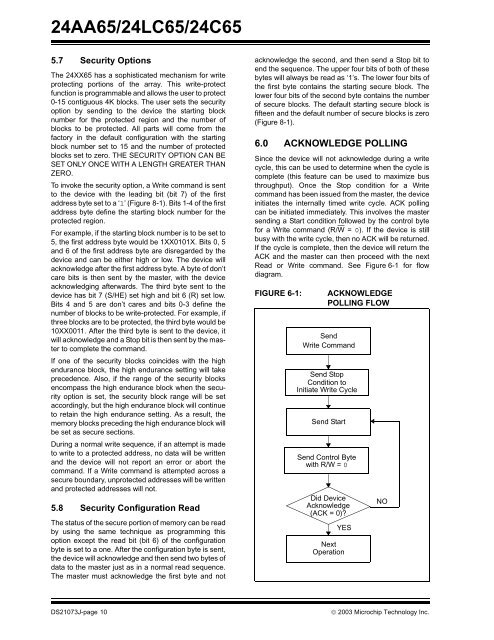
6.0 ACKNOWLEDGE POLLING<br />
Since the device will not acknowledge during a write<br />
cycle, this can be used to determine when the cycle is<br />
complete (this feature can be used to maximize bus<br />
throughput). Once the Stop condition for a Write<br />
command has been issued from the master, the device<br />
initiates the internally timed write cycle. ACK polling<br />
can be initiated immediately. This involves the master<br />
sending a Start condition followed by the control byte<br />
for a Write command (R/W = 0). If the device is still<br />
busy with the write cycle, then no ACK will be returned.<br />
If the cycle is complete, then the device will return the<br />
ACK and the master can then proceed with the next<br />
Read or Write command. See Figure 6-1 for flow<br />
diagram.<br />
FIGURE 6-1:<br />
ACKNOWLEDGE<br />
POLLING FLOW<br />
Send<br />
Write Command<br />
Send Stop<br />
Condition to<br />
Initiate Write Cycle<br />
Send Start<br />
Send Control Byte<br />
with R/W = 0<br />
Did Device<br />
Acknowledge<br />
(ACK = 0)?<br />
YES<br />
Next<br />
Operation<br />
NO<br />
DS21073J-page 10<br />
© 2003 <strong>Microchip</strong> Technology Inc.