158
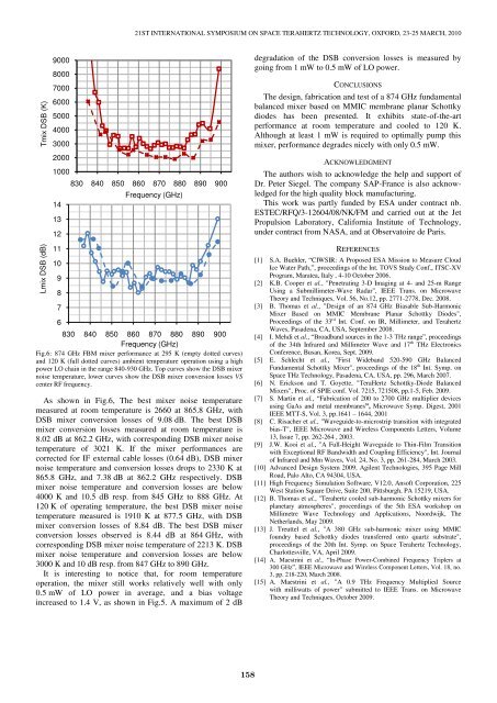
21ST INTERNATIONAL SYMPOSIUM ON SPACE TERAHERTZ TECHNOLOGY, OXFORD, 23-25 MARCH, 2010 183 GHz Mixer on InGaAs <strong>Schottky</strong> <strong>Diodes</strong> I. Oprea 1,3 , A. Walber 2 , O. Cojocari 1* , H. Gibson 2 , R. Zimmermann 2 , <strong>and</strong> H. L. Hartnagel 3 1 ACST GmbH, Darmstadt, Germany 2 RPG Radiometer <strong>Physics</strong> GmbH, Germany 3 Technische Universität Darmstadt, Darmstadt, Germany *Contact: cojocari@acst.de, phone +49-6151-162762 Abstract This work reports on experimental results <strong>of</strong> a 183 GHz sub-harmonically pumped mixer based on InGaAs antiparallel diode pair. The diode structure provides extremely low parasitic capacitance <strong>of</strong> about 2.5 fF. Roughly estimated series resistance junction capacitance <strong>and</strong> ideality factor 10, 4fF/anode <strong>and</strong> 1.2, respectively. The optimal LO-Power is as low as 0.34 mW, whereas usable performance can be achieved even with less than 0.2 mW. I. INTRODUCTION The <strong>Schottky</strong> junction is a generic technology, needed not only in space instruments but in practically all millimeter <strong>and</strong> sub-millimetre equipment, with the imaging evolving fast to become the primary area <strong>of</strong> application. During the last years the rapid progress in the development <strong>of</strong> <strong>Schottky</strong> technology has allowed efficient heterodyne receiver systems at frequencies up to 1.5 THz [1][3]. As the applications require a constant rise <strong>of</strong> the operation frequency, the expense <strong>of</strong> LO power used to drive the diode to the needed conductance is still a concern. A reduction <strong>of</strong> the LO frequency <strong>and</strong> thus the LO power requirements is possible by using subharmonically pumped mixers (SHM), where normally the LO is one half the RF frequency. GaAs antiparallel <strong>Schottky</strong> <strong>Diodes</strong> used in subharmonic mixer unfortunately require a significant DC bias or high LO power to drive the diode to an optimum conversion performance. Since it is difficult to bias diodes in this way the low <strong>Schottky</strong> barrier height <strong>of</strong> InGaAs material reduces the required LO power relative to diodes based on GaAs [4], [5]. <strong>Schottky</strong> barriers formed from In x Ga 1-x As have a height that decreases with increasing indium mole fraction. A lower barrier height means that a smaller LO Power is required to effectively pump the diode. The higher electron mobility in InGaAs in comparison to GaAs should play a role in minimising the series resistance which will reduce the conversion losses especially at higher frequencies. InGaAs mixers are also very interesting for potential use in integrated InP based millimetre <strong>and</strong> submillimetre wave receivers with state-<strong>of</strong>-the-art noise performance. II. ANTI-PARALLEL DIODE PARAMETER DETAILS The anti-parallel diode (APD) was fabricated by so-called Film-Diode process, which has been particularly developed at ACST for THz devices <strong>and</strong> circuits. The diode structure is based on the Quasi-vertical diode design, developed at Technical University <strong>of</strong> Darmstadt [6] <strong>and</strong> represents a discrete <strong>Schottky</strong> structure suitable for hybrid integration. In contrast to traditional planar structures, Film-Diode fabrication implies two-side processing <strong>of</strong> the semiconductor wafer, which implies a more complex fabrication, but is more flexible concerning the reduction <strong>of</strong> structure parasitics. In turn this provides a better potential for improving performance <strong>and</strong> allows operation at higher frequencies. The APD mixer diodes use an In 0.53 Ga 0.47 As active layer with a doping level <strong>of</strong> 8x10 16 cm -3 which is lattice matched grown on an InP substrate. Recently Schlecht [7] discussed the principle <strong>of</strong> an In 0.25 Ga 0.75 As based <strong>Schottky</strong> mixer, but no experimental results have been shown. Moreover the epitaxial growth <strong>of</strong> material with this indium mole fraction will not be lattice matched to InP <strong>and</strong> have much stress. The structures have 1.2 µm anodes in diameter <strong>and</strong> estimated zero bias junction capacitance per anode is about 4fF. The employed Film-Diode approach uses a transferred membrane substrate process which provides for strongly reduced structure parasitics. The shunt capacitance <strong>of</strong> APD diodes is as low as 2.5fF. The series resistance R s is extracted from simple I-V measurements <strong>and</strong> is slightly higher than expected. The high value <strong>of</strong> R s , approximately 10, can be caused by the wafer layout which was not optimised for mixing applications. On the other side the ideality factor is 1.2 <strong>and</strong> is comparable to GaAs diodes. The calculated <strong>Schottky</strong> barrier height is around 0.21 eV <strong>and</strong> is about one quarter <strong>of</strong> the value for similar GaAs diodes. Figure 1 shows the typical I-V curves <strong>of</strong> an InGaAs <strong>and</strong> GaAs diode measured on-wafer. The typical turn-on voltage (1µA) for fabricated InGaAs diodes is below 50µV, which is drastically reduced in comparison to GaAs diodes. Fig. 1. Measured I-V Curves <strong>of</strong> InGaAs <strong>and</strong> GaAs <strong>Schottky</strong> <strong>Diodes</strong> 159