Session S6: Schottky Diodes and Mixers - Department of Physics
Session S6: Schottky Diodes and Mixers - Department of Physics
Session S6: Schottky Diodes and Mixers - Department of Physics

Create successful ePaper yourself
Turn your PDF publications into a flip-book with our unique Google optimized e-Paper software.
21ST INTERNATIONAL SYMPOSIUM ON SPACE TERAHERTZ TECHNOLOGY, OXFORD, 23-25 MARCH, 2010<br />
Two diode-MMIC wafers were fabricated at JPL using the<br />
very successful membrane process developed for Hershel<br />
HIFI [3]. The wafers had epi-layer doping <strong>of</strong> 5x10 17 /cm 3<br />
<strong>and</strong> 2x10 17 with identical circuit layouts. Variations <strong>of</strong> the<br />
design were scaled to as high as 3.5 THz, but tests reported<br />
here are <strong>of</strong> only the 1.5 THz design. Simulations <strong>of</strong> the<br />
performance <strong>of</strong> these designs indicate a relatively flat RF<br />
fractional b<strong>and</strong>width <strong>of</strong> 25%. Upconverted power is limited<br />
by the input power which is very constrained in a circuit with<br />
just two anodes, since the anodes must be very small for<br />
proper impedance matching. The required capacitance Cj(0)<br />
is 1 fF at 1.5 THz yielding an anode diameter <strong>of</strong> 0.5 m<br />
(scaling downward with increasing frequency). However, it<br />
is practical to add anodes in series, as has been done with<br />
multiplier circuits [4] In principle, using two anodes in series<br />
increases the maximum input power by a factor <strong>of</strong> four,<br />
assuming that the failure mechanism is related to power<br />
density within the device. This scaling comes about because<br />
for the same impedance level, each device can have twice the<br />
area if two devices are in series. In the case <strong>of</strong> failure due to<br />
heating, the scaling is much less obvious, since it depends on<br />
thermal pathways within the complete circuit, not just local<br />
device properties, but there is still some significant<br />
advantage. Four-anode devices were fabricated but the<br />
anode size was only 1.5 times larger so the maximum power<br />
in this case should only increase a factor <strong>of</strong> three.<br />
The best results were obtained with the 5x10¹⁷ doping<br />
devices, but this wafer yield is quite low, ~35% for 2-anode<br />
devices, <strong>and</strong> the yield seems to be near zero for 4-anode<br />
devices. The wafer with 2x10 17 doping works acceptably at<br />
1.5 THz, but it is clear that the doping is too low. This wafer<br />
has a high yield <strong>of</strong> 2-anode devices <strong>and</strong> 30% yield <strong>of</strong> 4-anode<br />
devices.<br />
As is apparent from Fig 2, these are very small devices.<br />
While the GaAs membrane can not be touched, the beam<br />
leads can be h<strong>and</strong>led safely, <strong>and</strong> installation in the block is<br />
done by positioning the device with a micro-manipulator.<br />
Once positioned, conductive epoxy is applied to the IF <strong>and</strong><br />
bias port leads. Because <strong>of</strong> the small contact area this can<br />
result in a high contact resistance, <strong>and</strong> a solder contact would<br />
be preferred, but is much more difficult to produce.<br />
The block was machined in brass as an E-plane split-block<br />
using conventional tools with a CNC micro-milling machine<br />
[5] <strong>and</strong> the block was then gold plated. Both waveguides are<br />
80 x 160 um, stepping up to square cross section before<br />
transitioning to diagonal feedhorns on both input <strong>and</strong> output<br />
ports. The diagonal aperture sizes <strong>of</strong> each were 1.5 mm.<br />
Details <strong>of</strong> the block are shown in Figs 3 <strong>and</strong> 5. The diode<br />
was installed with the beamleads clamped between the halves<br />
<strong>of</strong> the block. The IF port used a K type connector to allow<br />
tests up to 40 GHz, but in fact no dimension or circuit<br />
capacitance inherent to the design limits the b<strong>and</strong>width below<br />
~150 GHz. For practical reasons <strong>of</strong> testing <strong>and</strong> machining,<br />
the input waveguide was bent to align with the axis <strong>of</strong> the<br />
output guide. This adds LO loss but this is not a concern<br />
with laser sources.<br />
III. UPCONVERSION RESULTS<br />
Upconversion tests were done using an optically pumped<br />
laser at 1561 GHz, with an available power level <strong>of</strong> >10 mW<br />
<strong>and</strong> a variable attenuator before the mixer input. The IF was<br />
10 GHz from a synthesizer. For the tests with the 5x10 17<br />
doping devices, only 2-anode devices were available. Four<br />
mixers were assembled with these devices. These were<br />
driven with a laser power <strong>of</strong> ~1.5 mW (as measured by a<br />
coupling aperture comparable to that <strong>of</strong> the feed horn).<br />
<strong>Diodes</strong> were forward biased in operation, with the<br />
conversion efficiency rising with bias up to 1 mA (which was<br />
the maximum used). With an IF power <strong>of</strong> 1.5 mW, the<br />
output power from the best device in the two sideb<strong>and</strong>s is 45<br />
µW with only 5 µW <strong>of</strong> LO feedthrough (~25 dB LO-RF<br />
isolation). The feedthrough power was measured with the IF<br />
signal <strong>of</strong>f, but there is the possibility that the feedthrough<br />
may increase with IF applied. In previous tests with a similar<br />
mixer a very narrow b<strong>and</strong> FPI etalon was used to separate the<br />
LO from the sideb<strong>and</strong> signals. Use <strong>of</strong> this filter showed that<br />
there was no change in LO feedthrough with the IF applied.<br />
The THz input <strong>and</strong> output power were measured with a<br />
waveguide calorimeter (Erickson Instruments PM4) [6] built<br />
in WR10 waveguide with no transition between the horn <strong>and</strong><br />
the waveguide in the sensor. The size <strong>of</strong> the horns <strong>and</strong><br />
WR10 waveguide are fairly similar so coupling was expected<br />
to be good. For two other devices taken from very nearby<br />
on the wafer, output power was within 10%, while the fourth<br />
device from another region produced only 18 W.<br />
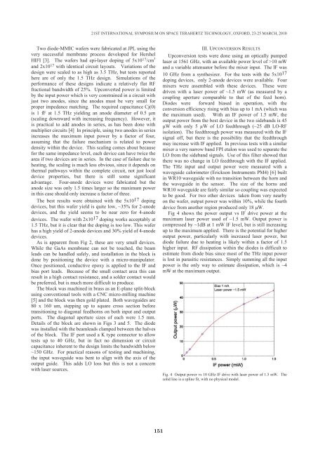
Fig 4 shows the power output vs IF drive power at the<br />
maximum laser power used <strong>of</strong> ~1.5 mW. Output power is<br />
compressed by ~1dB at 1 mW IF level, but is still increasing<br />
up to the maximum applied. There is the potential for higher<br />
output power, particularly with increased laser power, but<br />
diode failure due to heating is likely within a factor <strong>of</strong> 1.5<br />
higher input. RF dissipation within the diodes is difficult to<br />
estimate from diode bias since most <strong>of</strong> the THz input power<br />
is lost in parasitic resistances. Simply summing all the input<br />
power is the only way to estimate dissipation, which is ~4<br />
mW at the maximum output.<br />
Fig. 4 Output power vs 10 GHz IF drive with laser power <strong>of</strong> 1.5 mW. The<br />
solid line is a spline fit, with no physical model.<br />
151