Characteristics Of Ingan~algan Multiple-quantum-well Laser Diodes ...
Characteristics Of Ingan~algan Multiple-quantum-well Laser Diodes ...
Characteristics Of Ingan~algan Multiple-quantum-well Laser Diodes ...

You also want an ePaper? Increase the reach of your titles
YUMPU automatically turns print PDFs into web optimized ePapers that Google loves.
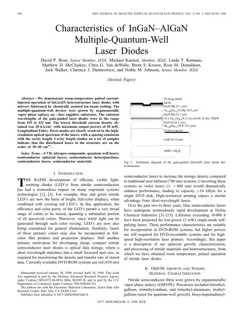
498 IEEE JOURNAL OF SELECTED TOPICS IN QUANTUM ELECTRONICS, VOL. 4, NO. 3, MAY/JUNE 1998<br />
<strong>Characteristics</strong> of InGaN–AlGaN<br />
<strong>Multiple</strong>-Quantum-Well<br />
<strong>Laser</strong> <strong>Diodes</strong><br />
David P. Bour, Senior Member, IEEE, Michael Kneissl, Member, IEEE, Linda T. Romano,<br />
Matthew D. McCluskey, Chris G. Van deWalle, Brent S. Krusor, Rose M. Donaldson,<br />
Jack Walker, Clarence J. Dunnrowicz, and Noble M. Johnson, Senior Member, IEEE<br />
(Invited Paper)<br />
Abstract—We demonstrate room-temperature pulsed currentinjected<br />
operation of InGaAlN heterostructure laser diodes with<br />
mirrors fabricated by chemically assisted ion beam etching. The<br />
multiple-<strong>quantum</strong>-<strong>well</strong> devices were grown by organometallic<br />
vapor phase epitaxy on c-face sapphire substrates. The emission<br />
wavelengths of the gain-guided laser diodes were in the range<br />
from 419 to 432 nm. The lowest threshold current density obtained<br />
was 20 kA/cm 2 with maximum output powers of 50 mW.<br />
Longitudinal Fabry–Perot modes are clearly resolved in the highresolution<br />
optical spectrum of the lasers, with a spacing consistent<br />
with the cavity length. Cavity length studies on a set of samples<br />
indicate that the distributed losses in the structure are on the<br />
order of 30–40 cm 01 .<br />
Index Terms—CVD, nitrogen compounds, <strong>quantum</strong> <strong>well</strong> lasers,<br />
semiconductor epitaxial layers, semiconductor heterojunctions,<br />
semiconductor lasers, semiconductor materials.<br />
I. INTRODUCTION<br />
THE RAPID development of efficient, visible lightemitting<br />
diodes (LED’s) from nitride semiconductors<br />
has had a tremendous impact on many important systems<br />
technologies [1], [2]. For example, blue and green nitride<br />
LED’s are now the basis of bright, full-color displays, when<br />
combined with existing red LED’s. In this application, the<br />
efficiency and color purity of the LED’s permit a very broad<br />
range of colors to be mixed, spanning a substantial portion<br />
of all perceived colors. Moreover, since white light can be<br />
generated through such color mixing, LED’s are now also<br />
being considered for general illumination. Similarly, lasers<br />
of these primary colors may also be incorporated in fullcolor<br />
film printers and projection displays. Still another<br />
primary motivation for developing cheap, compact nitride<br />
semiconductor laser diodes is optical data storage, where a<br />
short wavelength translates into a small focussed spot size, as<br />
required for maximizing the density and transfer rate of stored<br />
data. Currently available DVD-ROM systems use red (650 nm)<br />
Manuscript received January 26, 1998; revised April 14, 1998. This work<br />
was supported in part by the Defense Advanced Research Projects Agency<br />
under Contract MDA972-96-0014 (Blue BAND II) and in part by the U.S.<br />
Department of Commerce under Contract 70NANB2H1241.<br />
The authors are with the Electronic Materials Laboratory, Xerox Palo Alto<br />
Research Center, Palo Alto, CA 94304 USA.<br />
Publisher Item Identifier S 1077-260X(98)05446-X.<br />
Fig. 1. Schematic diagram of the gain-guided InGaAlN laser diode heterostructure.<br />
semiconductor lasers to increase the storage density compared<br />
to traditional near-infrared (780 nm) systems. Converting these<br />
systems to violet lasers ( 400 nm) would dramatically<br />
enhance performance, leading to capacity 10 Gbyte for a<br />
single DVD disk. High-resolution printing enjoys a similar<br />
advantage from short-wavelength lasers.<br />
Over the past two to three years, blue semiconductor lasers<br />
have undergone tremendously rapid development at Nichia<br />
Chemical Industries [3]–[15]. Lifetimes exceeding 10 000 h<br />
have been projected for low-power (2 mW) single-mode selfpulsing<br />
lasers. These performance characteristics are suitable<br />
for incorporation in DVD-ROM systems; but higher powers<br />
are still required for DVD-recordable systems and for highspeed<br />
high-resolution laser printers. Accordingly, this paper<br />
is a description of our epitaxial growth, characterization,<br />
and processing of nitride materials and heterostructures, from<br />
which we have obtained room temperature, pulsed operation<br />
of nitride laser diodes.<br />
II. OMVPE GROWTH AND NITRIDE<br />
MATERIAL CHARACTERIZATION<br />
Nitride semiconductor films were grown by organometallic<br />
vapor phase epitaxy (OMVPE). Precursors included trimethylgallium,<br />
trimethyl-indium, and trimethyl-aluminum, triethylgallium<br />
(used for <strong>quantum</strong>-<strong>well</strong> growth), biscyclopentadienyl-<br />
1077–260X/98$10.00 © 1998 IEEE
BOUR et al.: CHARACTERISTICS OF InGaN–AlGaN MQW LASER DIODES 499<br />
magnesium, dilute (10 ppm) silane, and purified ammonia.<br />
Growth was performed over -face (0001) sapphire substrates,<br />
beginning with a thin (30 nm) low-temperature (550 C)<br />
GaN nucleation layer, as is typically described in the literature<br />
[1], [3], [6], [8]. The device structure, shown in<br />
Fig. 1, includes a 4- m GaN:Si lateral n-contact layer, 0.4-<br />
mAl Ga N cladding layers, a 10 In Ga N–GaN<br />
(2 nm/6 nm) multiple-<strong>quantum</strong>-<strong>well</strong> (MQW) active region<br />
surrounded by 0.1- m GaN:Si, Mg waveguide layers, and<br />
a 0.1- m GaN:Mg p-contact layer. To activate the p-type<br />
conductivity in the Mg-doped layers, an 850 C, 5-min anneal<br />
was conducted, in a N ambient [16].<br />
Adequate levels of p-type doping are essential for successful<br />
operation of the device structure depicted in Fig. 1. We have<br />
performed a comprehensive theoretical investigation of acceptor<br />
doping in GaN, using first-principles calculations based<br />
on density-functional theory and ab initio pseudopotentials<br />
[17]. Incorporation of Mg on interstitial or substitutional<br />
nitrogen sites has often been invoked to explain limited hole<br />
concentrations; however, the calculations show that this type<br />
of incorporation is energetically unfavorable [18]. We found<br />
that the determining factor is the solubility of Mg in GaN,<br />
which is limited by competition between incorporation of Mg<br />
acceptors and formation of Mg N .<br />
We have also performed an extensive computational investigation<br />
of other acceptor impurities in GaN [19]. None of<br />
the candidate impurities (Na, Li, Be, Ca, Zn, and C) exhibit<br />
characteristics superior to Mg. Only Be has a comparable<br />
solubility and potentially lower ionization energy. Be doping<br />
is likely to be severely hampered, however, by incorporation<br />
of Be donors on interstitial sites. A certain degree of<br />
compensation by native defects does occur in p-type GaN, in<br />
particular by nitrogen vacancies; however, such compensation<br />
is significantly suppressed in the presence of hydrogen [20].<br />
Compensation by nitrogen vacancies becomes increasingly<br />
severe with increasing Al content in AlGaN alloys [21]. In<br />
addition, we calculate an increase in the ionization energy<br />
of the Mg acceptor with increasing Al content. These factors<br />
explain the increased difficulty in p-type doping of AlGaN.<br />
In addition to p-type doping, the structural and optoelectronic<br />
quality of the InGaN MQW active region is critically<br />
important in achieving nitride laser operation. The structural<br />
quality of the InGaN QW’s of a laser diode structure is<br />
apparent in the transmission electron microscope (TEM) image<br />
shown in Fig. 2. The layer thicknesses are uniform, with<br />
sharp interfaces between the InGaN QW’s and GaN barriers.<br />
From this micrograph, the layer thicknesses are determined<br />
to be 2 nm for the InGaN <strong>well</strong> layers, and 6 nm for the<br />
GaN barriers. From the TEM image, there is no evidence<br />
of InGaN phase segregation, although the existence of minor<br />
composition fluctuations cannot be ruled out [22]–[27].<br />
Likewise, X-ray diffraction from InGaN MQW’s also suggests<br />
that for these compositions and thicknesses used for laser<br />
diodes, alloy segregation is not significant. Fig. 3 shows the<br />
X-ray diffraction spectrum of an MQW active region, like that<br />
which has been incorporated into InGaN laser diodes (but with<br />
no AlGaN cladding layers). This structure contains ten 20-Å<br />
In Ga N QW’s, separated by 50-Å GaN barriers. Evidence<br />
Fig. 2. Transmission electron microscope image showing the MQW active<br />
region of an InGaN–GaN laser diode structure.<br />
Fig. 3.<br />
(006) X-ray diffraction pattern of a InGaN–GaN MQW structure.<br />
of the layer uniformity is indicated by coherent reflections<br />
from the periodic multilayers comprising the active region,<br />
which give rise to visible first, second, and thirdorder<br />
satellite peaks in the XRD spectrum. The presence of<br />
these peaks in the XRD spectrum demands that the layer<br />
compositions and thicknesses be uniform and periodic, which<br />
would not be the case if the InGaN were highly segregated.<br />
The spacing of the satellite peaks indicates the period of the<br />
superlattice active region to be about 70 Å. Likewise, the<br />
absolute position of the 0th-order peak indicates the average<br />
InGaN composition to be In Ga N.<br />
III. LED CHARACTERISTICS<br />
The spectral purity and brightness of laser diode wafers,<br />
measured below threshold as LED’s, is a useful diagnostic<br />
tool for rapidly assessing the quality of materials and<br />
heterostructures, with a structure that is much simpler to<br />
fabricate than a laser diode. Accordingly, simple, 250- m dot<br />
LED’s were fabricated from laser diode heterostructures by<br />
depositing Ti–Au p-contact metal, and dry-etching down to the<br />
4- m n-type GaN layer underlying the heterostructure, thereby<br />
defining 250- m dots. Contact to the n-type semiconductor<br />
was made simply with a probe tip touching the exposed<br />
GaN:Si (no n-metal was deposited). The LED wafers were then<br />
probed and operated while lying on a quartz wafer, so that the<br />
emission through the substrate could be detected and analyzed.<br />
The pulsed power output (spontaneous emission) of a working
500 IEEE JOURNAL OF SELECTED TOPICS IN QUANTUM ELECTRONICS, VOL. 4, NO. 3, MAY/JUNE 1998<br />
Fig. 4. L–I characteristic of a InGaN–GaN MQW laser diode structure<br />
tested as LED.<br />
InGaN–AlGaN 10-QW laser diode heterostructure, measured<br />
for this geometry where only the light emitted through the<br />
bottom of the wafer is detected, is shown in Fig. 4 as a function<br />
of the injection current. The bottom-emitted power exceeds 70<br />
mW at 500 mA, with a differential <strong>quantum</strong> efficiency of 5%.<br />
This value indicates that the internal <strong>quantum</strong> efficiency of the<br />
InGaN MQW’s is reasonably high.<br />
The structural quality of the InGaN MQW’s is also evident<br />
in the spectral purity of the spontaneous emission from a<br />
working laser diode heterostructure (this sample has a structure<br />
like that in Fig. 1, and contains ten 20-Å In Ga N–GaN<br />
QW’s and Al Ga N cladding layers). As shown in Fig. 5<br />
for several values of dc bias, the spectrum is centered at<br />
422 nm, and the full-width at half-maximum (FWHM) of<br />
the spectrum is 16 nm. Most significantly, over more than<br />
three decades of dc injection current (20 A 80 mA,<br />
corresponding to a current density 0.04 160 A/cm ), it<br />
is apparent that no large spectral shifts occur. Instead, only a<br />
gradual shift toward longer wavelength occurs at high currents,<br />
consistent with heating. This spectral purity with respect<br />
to injected carrier density indicates that the InGaN alloy<br />
active region composition is relatively uniform. In contrast,<br />
some structural deterioration (possibly, but not necessarily<br />
alloy segregation [27]) is evident when the QW’s are made<br />
either thicker, with higher indium content, or more numerous.<br />
In these cases, structural defects are reflected in spectrally<br />
broad emission, which also undergoes large (sometimes discontinuous)<br />
shifts to shorter wavelengths as the injection<br />
current is increased. Thus, taken together with the TEM image<br />
(Fig. 2) and the X-ray diffraction (Fig. 3), the spectral purity<br />
of the spontaneous emission from these InGaN–AlGaN MQW<br />
laser diode samples indicates that InGaN alloy segregation<br />
has largely been avoided for the chosen QW composition,<br />
thickness and number of QW’s.<br />
IV. LASER DIODE CHARACTERISTICS<br />
While there is no evidence that the InGaN comprising our<br />
MQW active region is segregated, we cannot eliminate the<br />
possibility of slight alloy segregation. Indeed, the spectra of<br />
Fig. 5 are still measurably broader (16-nm FWHM) than the<br />
emission from MQW’s of lower indium content (8–10-nm<br />
FWHM for emission wavelengths 390–400 nm). This spectral<br />
Fig. 5. Emission spectra of InGaN–AlGaN MQW LED at various injection<br />
currents from 20 A < I
BOUR et al.: CHARACTERISTICS OF InGaN–AlGaN MQW LASER DIODES 501<br />
overcome with additional optical gain. Finally, further losses<br />
may also arise from the inability to realize nitride waveguide<br />
heterostructures which completely contain either the injected<br />
carriers [31], [32] or the optical mode [15]. In this case,<br />
because the AlGaN cladding layers experience biaxial tension<br />
when grown over GaN or InGaN, they tend to crack. As<br />
a result, the cladding layer aluminum content and thickness<br />
are limited to values which may not completely contain the<br />
evanescent tail of the optical mode. Instead, some of the<br />
light is able to leak out of the guide, thereby contributing<br />
to outcoupling or absorption losses. In particular, light may be<br />
outcoupled from the waveguide, into the thick GaN underlying<br />
the heterostructure; or the optical mode may penetrate into the<br />
p-metal contact, where it is strongly absorbed. Consequently,<br />
producing sufficient optical gain to overcome these loss mechanisms,<br />
while still maintaining the InGaN’s excellent structural<br />
integrity, has required multiple, thin QW’s.<br />
With respect to optical confinement, a cladding layer with<br />
high aluminum content is essential for maximizing the spatial<br />
overlap between the optical mode and the QW gain. This<br />
requirement, however must be traded off against the p-doping<br />
difficulties and the tendency to crack, both of which are<br />
problems associated with high-aluminum-content AlGaN films<br />
[15]. These difficulties could be avoided by eliminating the<br />
AlGaN cladding layers; and instead creating a waveguide with<br />
a large number of high-indium-content InGaN QW’s in the<br />
active region. However, for a large number of QW’s, it may<br />
become difficult to achieve good spatial overlap between the<br />
injected electron and hole distributions, since they are injected<br />
from opposite sides of the QW stack. Likewise, confinement<br />
of injected carriers would also suffer [31], [32]. Overall, there<br />
exist a multitude of tradeoffs that must be considered in the<br />
design of nitride laser structures.<br />
We have observed pulsed laser oscillation at room temperature,<br />
with an InGaN–AlGaN multiple QW injection laser<br />
heterostructures, of the structure shown in Fig. 1. Gain-guided<br />
devices were fabricated using silicon oxy-nitride dielectric<br />
insulating layers, with stripe openings of 4, 10, or 20 m.<br />
Both n- and p-contact metallizations were made using Ti–Au.<br />
Mirrors were etched using CAIBE (chemically assisted ion<br />
beam etching), to define cavity lengths of 300, 500, 800, or<br />
1000 m. In the CAIBE technique, the mechanical etching<br />
component (Ar–ion milling current and acceleration voltage)<br />
and the chemical etching component (Cl –BCl reactive gas<br />
flows and wafer temperature) are independently adjustable.<br />
By optimizing these parameters, combined with the proper<br />
wafer tilt angle, vertical and smooth laser mirrors can be<br />
realized [14], [33]. Surface profiles of CAIBE-etched mirrors,<br />
measured using atomic force microscopy, reveal an root-meansquared<br />
roughness of 4–5 nm. Based on optical pumping<br />
experiments, the reflectivity of these mirrors is estimated to be<br />
about 70% of the ideal value [14]. Presumably, some fraction<br />
of the incident light is scattered by the slight surface roughness,<br />
which is currently limited by the photoresist mask. In principle,<br />
more sophisticated, multilayer etch masks could be used to<br />
produce even smoother mirrors using CAIBE.<br />
The light-output intensity is shown as a function of the<br />
injection current in Fig. 6, for a 10 m 800 m diode<br />
Fig. 6. Measured I–V and L–I output power for a 10 2 800 m 2 laser<br />
diode (uncoated mirrors).<br />
Fig. 7. High-resolution optical spectrum for a 4 2 300 m 2 diode operating<br />
above threshold (I = 740 mA).<br />
operated pulsed at room temperature (pulse width 500 ns,<br />
repetition rate 1 kHz), with uncoated mirrors. The –<br />
characteristic exhibits a threshold current of about 1.9 A,<br />
corresponding to a threshold current density of 24 kA/cm .<br />
Using a calibrated silicon p-i-n diode detector, the peak power<br />
was measured to be 50 mW. This value probably represents<br />
a conservative estimate of the emitted power, because of the<br />
difficulty associated with collecting all the emitted light from<br />
an etched-mirror laser, where part of the beam is intercepted<br />
by the substrate. The emission was TE-polarized; and at<br />
threshold, the far-field emission pattern collapsed into a beam<br />
characteristic of an etched-facet laser. The beam was elliptical,<br />
with a divergence angle narrower in the junction plane than<br />
in the vertical direction. The transverse beam divergence was<br />
difficult to measure, however, because the transverse far-field<br />
pattern exhibited a strong modulation, arising from interference<br />
between the directly emitted beam and the component<br />
of the beam, which was reflected from the etched surface.<br />
The far-field was therefore very similar to that of the first<br />
nitride laser diode demonstrated by Nakamura et al., which<br />
also had etched facets [3]. The voltage versus current ( – )<br />
characteristic is also shown in Fig. 6. The threshold voltage<br />
is approximately 19 V.<br />
An emission spectrum is shown in Fig. 7, for a<br />
4 m 300 m device operated at 740 mA. The longitudinal<br />
Fabry–Perot mode spacing of 0.091 nm is consistent with the<br />
cavity length of 300 m (giving a reasonable value of 3.22 for
502 IEEE JOURNAL OF SELECTED TOPICS IN QUANTUM ELECTRONICS, VOL. 4, NO. 3, MAY/JUNE 1998<br />
Fabry–Perot modes are clearly resolved in the high-resolution<br />
optical spectrum of the lasers, with a spacing consistent with<br />
the cavity length. Cavity length studies on a set of samples<br />
indicate that the distributed losses in the structure are in the<br />
order of 30–40 cm .<br />
ACKNOWLEDGMENT<br />
The authors are pleased to acknowledge helpful discussions<br />
with R. D. Bringans and D. Hofstetter; and to thank F. Endicott<br />
and E. Taggart for technical support.<br />
Fig. 8. Measured threshold current density for gain-guided InGaN–AlGaN<br />
laser diodes versus the inverse cavity length. The p-metal stripe width of the<br />
broad area test structures was 20 m; mirrors are uncoated.<br />
the dispersion-corrected index). Below threshold, the spectral<br />
width of the spontaneous emission was typically 15–20 nm.<br />
The threshold current density was found to have a strong<br />
dependence on the cavity length . This is shown in Fig. 8<br />
as a function of the inverse cavity length (since the mirror loss<br />
component of the total loss is proportional to ), for lasers<br />
with 20- m stripe width and uncoated mirrors. The threshold<br />
current density varies from 20 kA/cm for 10 cm<br />
( 1000 m), to 44 kA/cm for 33 cm (<br />
300 m). This strong variation suggests that the distributed<br />
loss is not so high as to overwhelm the mirror loss (<br />
, where is the mirror reflectivity); otherwise,<br />
the threshold current density would not exhibit a dependence<br />
on the cavity length. Since the mirror loss is approximately<br />
known, the distributed loss may be roughly estimated from<br />
the threshold current density measurements by assuming that<br />
the optical gain is simply proportional to the injection current.<br />
This assumption produces a straight-line fit to the threshold<br />
data (shown), from which the distributed loss is estimated<br />
to be 30–40 cm . The lasers represented in Figs. 5–8<br />
represent our lowest-threshold devices, with wavelength<br />
420 nm. Among several laser wafers tested, however, lasing<br />
wavelengths as long as 432 nm were achieved, although with<br />
higher thresholds.<br />
V. SUMMARY<br />
We have achieved room-temperature pulsed operation of<br />
InGaAlN heterostructure laser diodes with mirrors fabricated<br />
by chemically assisted ion beam etching. The devices were<br />
grown by organometallic vapor phase epitaxy (OMVPE) on<br />
-face sapphire substrates. The device structure contains ten<br />
20-Å In Ga N–GaN QW’s and Al Ga N cladding<br />
layers. The structural quality of the InGaN MQW active region<br />
is evident in transmission electron micrographs, spectrally pure<br />
spontaneous emission, and satellite peaks appearing in the X-<br />
ray diffraction spectrum. The emission wavelengths of the<br />
gain-guided laser diodes were in the range from 419 to 432 nm.<br />
The lowest threshold current density obtained was 20 kA/cm<br />
with maximum pulsed output powers of 50 mW. Longitudinal<br />
REFERENCES<br />
[1] S. Nakamura, M. Senoh, N. Iwasa, and S. Nagahama, “High-power<br />
InGaN single-<strong>quantum</strong>-<strong>well</strong>-structure blue and violet light-emitting<br />
diodes,” Appl. Phys. Lett., vol. 67, pp. 1868–1870, Sept. 1995.<br />
[2] S. Nakamura, “A bright future for blue/green LED’s,” IEEE Circuits<br />
Devices, pp. 19–23, May 1995.<br />
[3] S. Nakamura, M. Senoh, S. Nagahama, N. Iwasa, T. Yamada, T. Matsushita,<br />
H. Kiyoku, and Y. Sugimoto, “InGaN-based MQW-structure<br />
laser diodes,” Jpn. J. Appl. Phys., vol. 35, pp. L74–L76, 1996.<br />
[4] S. Nakamura, M. Senoh, S. Nagahama, N. Iwasa, T. Yamada, T. Matsushita,<br />
Y. Sugimoto, and H. Kiyoku, “Room-temperature cw operation<br />
of InGaN MQW structure laser diodes,” Appl. Phys. Lett., vol. 69, pp.<br />
4056–4058, 1996.<br />
[5] S. Nakamura, M. Senoh, S. Nagahama, N. Iwasa, T. Yamada, T.<br />
Matsushita, Y. Sugimoto, and H. Kiyoku, “Ridge-geometry InGaN<br />
MQW structure laser diodes,” Appl. Phys. Lett., vol. 69, pp. 1477–1479,<br />
1996.<br />
[6] S. Nakamura, “InGaN-based blue laser diodes,” IEEE J. Select. Topics<br />
Quantum Electron., vol. 3, pp. 712–718, 1996.<br />
[7] I. Akasaki, H. Amano, S. Sota, H. Sakai, T. Tanaka, and M. Koike,<br />
“Stimulated emission by current injection from an AlGaN/GaN/GaInN<br />
<strong>quantum</strong> <strong>well</strong> device,” Jpn. J. Appl. Phys., vol. 34, pp. L1517–L1519,<br />
1995.<br />
[8] I. Akasaki and H. Amano, “Widegap column-III nitride semiconductors<br />
for UV/blue light emitting devices,” J. Electrochem. Soc., vol. 141, pp.<br />
2266–2271, 1994.<br />
[9] K. Itaya, M. Onomura, J. Nishio, L. Sugiura, S. Saito, M. Suzuki, J.<br />
Rennie, S. Nunoue, M. Yamamoto, H. Fujimoto, Y. Kokobun, Y. Ohba,<br />
G. Hatakoshi, and M. Ishikawa, “Room temperature pulsed operation of<br />
nitride-based MQW laser diodes with cleaved facets on conventional C-<br />
face sapphire substrates,” Jpn. J. Appl. Phys., vol. 35, pp. L1315–L1317,<br />
1996.<br />
[10] A. Kuramata, K. Domen, R. Soejima, K. Horino, S. Kubota, and T.<br />
Tanahashi, “InGaN laser diode grown on 6H-SiC using low pressure<br />
MOVPE,” in Proc. Int. Conf. Nitride Semiconductors (ICNS-97), 1997,<br />
pp. 450–451.<br />
[11] J. Edmond, G. Bulman, H. S. Kong, M. Leonard, K. Doverspike, W.<br />
Weeks, J. Niccum, S. Sheppard, G. Negley, and D. Slater, “Nitride-based<br />
emitters on SiC substrates,” in Proc. Int. Conf. Nitride Semiconductors<br />
(ICNS-97), 1997, pp. 448–449.<br />
[12] M. P. Mack, A. C. Abare, M. Aizcorbe, P. Kozodoy, S. Keller, U.<br />
Mishra, L. A. Coldren, and S. P. DenBaars, “Room temperature pulsed<br />
operation of blue nitride based laser diodes,” in Proc. Int. Conf. Nitride<br />
Semiconductors (ICNS-97), 1997, p. 458.<br />
[13] F. Nakamura, T. Kobayashi, T. Asatsuma, K. Funato, K. Yanashima,<br />
S. Hashimoto, K. Naganuma, S. Tomioka, T. Miyajima, E. Morita, H.<br />
Kawai, and M. Ikeda, “Room temperature pulsed operation of a GaInN<br />
MQW laser diode with an optimized <strong>well</strong> number,” in Proc. Int. Conf.<br />
Nitride Semiconductors (ICNS-97), 1997, p. 460.<br />
[14] M. Kneissl, D. Hofstetter, D. P. Bour, R. Donaldson, J. Walker, and N.<br />
M. Johnson, “Dry-etching and characterization of mirrors on III-nitride<br />
laser diodes from chemically assisted ion beam etching,” in Proc. Int.<br />
Conf. Nitride Semiconductors (ICNS-97), 1997, pp. 462–463.<br />
[15] S. Nakamura, M. Senoh, S. Nagahama, N. Iwasa, T. Yamada, T.<br />
Matsushita, H. Kiyoku, Y. Sugimoto, T. Kozaki, H. Umemoto, M.<br />
Sano, and K. Chocho, “Present status of InGaN/GaN/AlGaN-based laser<br />
diodes,” in Proc. Int. Conf. Nitride Semiconductors (ICNS-97), 1997, pp.<br />
444–445.
BOUR et al.: CHARACTERISTICS OF InGaN–AlGaN MQW LASER DIODES 503<br />
[16] W. Götz, N. M. Johnson, J. Walker, D. P. Bour, and R. A. Street,<br />
“Activation of acceptors in Mg-doped GaN grown by MOCVD,” Appl.<br />
Phys. Lett., vol. 68, pp. 667–669, 1996.<br />
[17] J. Neugebauer and C. G. Van de Walle, “Atomic geometry and electronic<br />
structure of native defects in GaN,” Phys. Rev. B, vol. 50, p. 8067, 1994.<br />
[18] , “Theory of point defects and complexes in GaN,” in Proc.<br />
Materials Research Soc. Symp., 1996, vol. 395, p. 645.<br />
[19] , “Defects and doping in GaN,” in Proc. ICPS-23. Singapore:<br />
World Scientific, 1996, p. 2849.<br />
[20] , “Role of hydrogen in doping of GaN,” Appl. Phys. Lett., vol.<br />
68, pp. 1829–1831, 1996.<br />
[21] C. Stampfl and C. G. Van de Walle, “Doping of Al x Ga 10xN,” Appl.<br />
Phys. Lett., vol. 72, no. 4, Jan. 26, 1998.<br />
[22] A. Wakahara, T. Tokuda, X. Dang, and S. Noda, “Compositional<br />
inhomogeneity and immiscibility of a GaInN ternary alloy,” Appl. Phys.<br />
Lett., vol. 71, pp. 906–908, Aug. 1997.<br />
[23] S. Nakamura, M. Senoh, S. Nagahama, N. Iwasa, T. Yamada, T.<br />
Matsushita, Y. Sugimoto, and H. Kiyoku, “Subband emissions of InGaN<br />
multi-<strong>quantum</strong>-<strong>well</strong> laser diodes under room-temperature continuous<br />
wave operation,” Appl. Phys. Lett., vol. 70, pp. 2753–2755, May 1997.<br />
[24] S. Chichubu, T. Azuhata, T. Sota, and S. Nakamura, “Luminescences<br />
from localized states in InGaN epilayers,” Appl. Phys. Lett., vol. 70, pp.<br />
2822–2824, May 1997.<br />
[25] Y. Narukawa, Y. Kawakami, M. Funato, S. Fujita, S. Fujita, and<br />
S. Nakamura, “Role of self-formed InGaN <strong>quantum</strong> dots for exciton<br />
localization in the purple laser diode emitting at 420 nm,” Appl. Phys.<br />
Lett., vol. 70, pp. 981–983, Feb. 1997.<br />
[26] M. Kuball, E. Jeon, Y. Song, A. Nurmikko, P. Kozodoy, A. Abare, S.<br />
Keller, L. Coldren, U. Mishra, S. DenBaars, and D. Steigerwald, “Gain<br />
spectroscopy of InGaN/GaN <strong>quantum</strong> <strong>well</strong> diodes,” Appl. Phys. Lett.,<br />
vol. 70, pp. 2580–2582, May 1997.<br />
[27] K. Hiramatsu, Y. Kawaguchi, M. Shimizu, N. Sawaki, T. Zheleva, R.<br />
Davis, H. Tsuda, W. Taki, N. Kuwano, and K. Oki, “The composition<br />
pulling effect in MOVPE grown InGaN on GaN and AlGaN and its<br />
TEM characterization,” MRS Internet J. Nitride Res., vol. 2, article 6,<br />
1997.<br />
[28] P. Rees, C. Cooper, P. Smowton, P. Blood, and J. Hegarty, “Calculated<br />
threshold currents of nitride- and phosphide-based <strong>quantum</strong>-<strong>well</strong> lasers,”<br />
IEEE Photon. Technol. Lett., vol. 8, pp. 197–199, Feb. 1996.<br />
[29] W. Chow, A. Knorr, and S. Koch, “Theory of laser gain in group-III<br />
nitrides,” Appl. Phys. Lett., vol. 67, pp. 754–756, Aug. 1995.<br />
[30] Z. Liau, R. L. Aggarwal, P. Maki, R. Molnar, J. Walpole, R. Williamson,<br />
and I. Melngailis, “Light scattering in high-dislocation-density GaN,”<br />
Appl. Phys. Lett., vol. 69, pp. 1665–1667, Sept. 1996.<br />
[31] G. Hatakoshi, K. Itaya, M. Ishikawa, M. Okajima, and Y. Uematsu,<br />
“Short-wavelength InGaAlP laser diodes,” IEEE J. Quantum Electron.,<br />
vol. 27, pp. 1476–1482, June 1991.<br />
[32] A. Ishibashi, “II-VI blue-green laser diodes,” IEEE J. Select. Topics<br />
Quantum Electron., vol. 1, pp. 741–748, June 1995.<br />
[33] M. Kneissl, D. P. Bour, N. M. Johnson, L. Romano, B. Krusor, R. Donaldson,<br />
J. Walker, C. Dunnrowicz, and R. Bringans, “Characterization of<br />
AlGaInN diode lasers with mirrors from chemically assisted ion beam<br />
etching,” Appl. Phys. Lett., vol. 72, pp. 1539–1541, Mar. 1998.<br />
David P. Bour (S’84–M’85–SM’97) was born on<br />
May 2, 1961, in Pittsburgh, PA. He received the<br />
B.S. degree in physics from the Massachusetts Institute<br />
of Technology, Cambridge, in 1983, and the<br />
Ph.D. degree in electrical engineering from Cornell<br />
University, Ithaca, NY, in 1987, where he worked<br />
on OMVPE growth of AlGaInP red semiconductor<br />
lasers.<br />
From 1987 to 1991, he worked on infrared Al-<br />
GaAs and InGaAsP laser diodes as a member of<br />
research staff at the David Sarnoff Research Center<br />
(formerly RCA Laboratories, Princeton, NJ). Since 1991 he has been with<br />
Xerox PARC, working first on red laser diodes and arrays for printing; and<br />
more recently he established a nitride semiconductor film growth capability at<br />
Xerox, for deposition of material for blue semiconductor lasers. He is currently<br />
a Principal Scientist in the Electronic Materials Laboratory of the Xerox Palo<br />
Alto Research Center (PARC), Palo Alto, CA.<br />
Michael Kneissl (M’98) was born in Schneckenlohe,<br />
Germany, in 1966. He received the Dipl.-<br />
Phys. degree and the Dr. rer. nat. degree, both in<br />
physics, from the University of Erlangen-Nürnberg,<br />
Germany, in 1992 and 1996, respectively. His graduate<br />
research work involved in the design, MBE<br />
growth and characterization of (In)GaAs–AlGaAs<br />
electrooptic modulator devices.<br />
During his graduate studies, he was also a Visiting<br />
Scholar at the University of California, Berkeley, in<br />
1993. At present he is a Member of Research Staff<br />
at the Xerox Palo Alto Research Center, Palo Alto, CA, where he is working<br />
on MOCVD growth, fabrication, and in particular dry-etching of III-nitrides<br />
using CAIBE, and characterization of AlGaInN laser diodes.<br />
Linda T. Romano was born in New York, NY. Her<br />
undergraduate study started at Purdue University<br />
in West Lafayette, IN, in a cooperative Materials<br />
Engineering work program with Caterpillar Tractor<br />
Company, Peoria, IL. She received the B.S. degree<br />
in 1980 and the Ph.D. degree in 1987 from the University<br />
of Illinois, Urbana-Champaign, in materials<br />
science. Her Ph.D. dissertation involved the growth<br />
and characterization of sputter deposited metastable<br />
(III–V) 10x (IV 2 ) x alloys.<br />
From 1987 to 1992, she was at Oxford University,<br />
Oxford, U.K., involved in structural studies of high-temperature oxide superconductors<br />
by transmission electron microscopy (TEM) in connection with<br />
the growth and electrical properties. At Oxford University, she also helped<br />
develop novel ways to use the techniques of Rutherford backscattering (RBS)<br />
and proton induced X-ray emisson (PIXE) for materials characterization. Since<br />
1992, she has been at Xerox Corporation’s Palo Alto Research Center working<br />
on materials for printing and laser applications. Currently, she is responsible<br />
for the structural characterization of nitride lasers with a major emphasis on<br />
transmission electron microscopy studies.<br />
Matthew D. McCluskey received the B.S. degree<br />
in physics from the Massachusetts Institute of Technology,<br />
Cambridge, MA, in 1991 and the Ph.D.<br />
degree in physics from the University of California,<br />
Berkeley, in 1997. His Ph.D. research involved<br />
local vibrational mode spectroscopy of defects in<br />
semiconductors.<br />
Since January of 1997, he has been a Research<br />
Associate at Xerox Palo Alto Research Center,<br />
where he is investigating the optical and structural<br />
properties of GaN-based heterostructures.<br />
Chris G. Van de Walle received the degree of<br />
Engineer from the University of Ghent, Belgium,<br />
in 1982, and the Ph.D. degree from Stanford University,<br />
Palo Alto, CA, in 1986.<br />
He is a Member of Research Staff at the Xerox<br />
Palo Alto Research Center, Palo Alto, CA. After<br />
a Post-Doctoral Fellowship at the IBM T. J.<br />
Watson Research Center, Yorktown Heights, NY<br />
(1986–1988), he was with Philips Laboratories in<br />
Briarcliff Manor, NY (1988–1991). His research<br />
activities address a wide variety of problems in materials<br />
physics using first-principles computations. He has performed extensive<br />
studies of semiconductor interfaces, including the development of a widely<br />
used model for band offsets. He also investigates defects and impurities in<br />
semiconductors, with particular emphasis on doping problems and on the role<br />
of hydrogen. Recently, he has been focusing on the III–V nitrides. He has<br />
authored over 120 scientific publications and holds two U.S. patents. He is a<br />
Divisional Associate Editor for Physical Review Letters.<br />
Dr. Van de Walle was a Fellow of the Belgian American Educational Foundation<br />
in 1982–1983. He chaired the 7th Trieste Semiconductor Symposium on<br />
Wide-Bandgap Semiconductors in 1992, the 23rd Conference on Physics and<br />
Chemistry of Semiconductor Interfaces in 1996, and is chairing the Gordon<br />
Research Conference on Point and Line Defects in Semiconductors in 1998.<br />
He is a Fellow of the American Physical Society.
504 IEEE JOURNAL OF SELECTED TOPICS IN QUANTUM ELECTRONICS, VOL. 4, NO. 3, MAY/JUNE 1998<br />
Rose M. Donaldson was born in Phoenix, Arizona,<br />
on January 7, 1954. She attended Mission College,<br />
Santa Clara, CA.<br />
She began working at Data General, Sunnyvale,<br />
CA working on single crystal epitaxy, and the fabrication<br />
of semiconductors and integrated circuits.<br />
Since 1985, she has been with Xerox Palo Alto Research<br />
Center, Palo Alto, CA, where she has worked<br />
on a variety of novel device architectures, including<br />
independently addressable array lasers, heterojunction<br />
bipolar transistors, and vertical-cavity surfaceemitting<br />
lasers.<br />
Brent S. Krusor was born on May 4, 1951, in Lincoln,<br />
NE. He received the B.S. degree in chemistry<br />
from the Massachusetts Institute of Technology,<br />
Cambridge, MA, in 1973 and the M.S. degree<br />
in chemistry from the University of California,<br />
Berkeley, in 1977.<br />
Since 1978, he has been with Xerox Palo Alto<br />
Research Center, Palo Alto, CA, where he is currently<br />
involved in the characterization of epitaxial<br />
thin films by high-resolution X-ray diffraction.<br />
Jack Walker received the B.A. degree in chemistry<br />
from Southwestern College, Winfield, KS, in 1957,<br />
and the M.S. degree in chemistry from Wichita State<br />
University, Wichita, KS, in 1960.<br />
He began working at Texas Instruments Incorporated,<br />
Dallas, TX, in 1966 and was involved with<br />
vapor phase epitaxial growth of GaAs and GaAsP<br />
and liquid phase epitaxial growth of GaAs and GaP.<br />
In 1973, he joined Monsanto in Cupertino, CA, and<br />
was involved in all phases of liquid and vapor phase<br />
epitaxy of III–V materials and also in substrate<br />
growth and preparation of GaAs and GaP, and also in all phases of III-V<br />
LED fabrication. In 1981, he joined Xerox Palo Alto Research Center, Palo<br />
Alto, CA, where he has processed and characterized material for red laser<br />
diodes and is presently processing and characterizing materials for III–N laser<br />
diodes and LED’s.<br />
Clarence J. Dunnrowicz received the B.S. degree<br />
in physics from Worcester Polytechnic Institute,<br />
Worcester, MA, in 1973. His senior project involved<br />
the design and construction of a argon–ion laser and<br />
pulse-forming network.<br />
From 1973 to 1980, he was employed at Raytheon<br />
Research where his primary focus involved the<br />
fabrication of surface-acoustic-wave (SAW) pulse<br />
compression devices and low-phase-noise oscillators<br />
for advanced radar systems. He is co-inventor<br />
of the “all-quartz package” concept for low aging,<br />
vibration insensitive SAW resonator-oscillators. From 1982 to 1996, he has<br />
been associated with various companies dealing with GaAs- and InP-based<br />
semiconductor devices for communications, sensing, and electronic warfare.<br />
Since joining Xerox Palo Alto Research Center (PARC), Palo Alto, CA, in<br />
1996, he has been involved with edge emitters, vertical cavity surface emitting<br />
lasers, and novel high density interconnection schemes. He holds five patents,<br />
and has published in the areas of SAW and millimeter-wave devices.<br />
Dr. Dunnrowicz is a member of SPIE/AVS.<br />
Noble M. Johnson (S’66–M’73–SM’86) received<br />
the Ph.D. degree from Princeton University, Princeton,<br />
NJ, in 1974 under a National Defense graduate<br />
Fellowship.<br />
From 1974 to 1976, he worked at SRI International,<br />
Menlo Park, CA, in the Radiation Physics<br />
Group of the Physical Sciences Division. In 1976,<br />
he joined the Xerox Palo Alto Research Center, Palo<br />
Alto, CA, as a Member of the Research Staff in<br />
the Electronic Materials Laboratory, where he is<br />
currently a Principal Scientist. He has conducted<br />
experimental research in the general areas of electronic materials and devices<br />
and particularly on the following: electronic defects in semiconductors (crystalline<br />
and amorphous), metal–insulator–semiconductor structures, deep-level<br />
transient spectroscopy, hydrogen in semiconductors, plasma-assisted synthesis<br />
of materials, and the development of InGaAlN materials for optoelectronic<br />
device applications. In 1986 (spring semester), he was a visiting lecturer at<br />
Princeton University.<br />
In 1987, Dr. Johnson received a Distinguished U.S. Scientist Award from<br />
the Alexander von Humboldt Foundation, Germany, and in 1988, under the<br />
auspices of the Humboldt Foundation, he was in residence at the Institute for<br />
Applied Physics, University of Erlangen-Nürnberg, Germany. He is a Fellow<br />
of the American Physical Society and a member of the Materials Research<br />
Society (an elected member of the Advisory Council, 1986–1988).