TKR-750 service manual
TKR-750 service manual
TKR-750 service manual

Create successful ePaper yourself
Turn your PDF publications into a flip-book with our unique Google optimized e-Paper software.
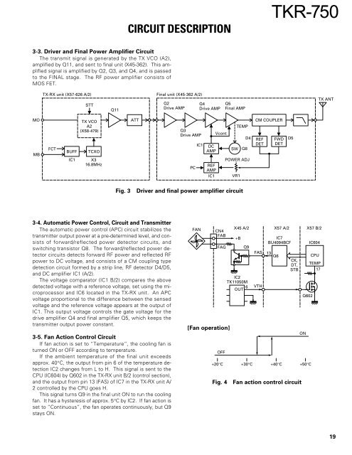
CIRCUIT DESCRIPTION<br />
<strong>TKR</strong>-<strong>750</strong><br />
3-3. Driver and Final Power Amplifier Circuit<br />
The transmit signal is generated by the TX VCO (A2),<br />
amplified by Q11, and sent to final unit (X45-362). This amplified<br />
signal is amplified by Q2, Q3, and Q4, and is passed<br />
to the FINAL stage. The RF power amplifier consists of<br />
MOS FET.<br />
TX-RX unit (X57-626 A/2)<br />
STT<br />
Q11<br />
Final unit (X45-362 A/2)<br />
Q2<br />
Drive AMP<br />
Q4<br />
Drive AMP<br />
Q5<br />
Final AMP<br />
TX ANT<br />
MO<br />
MB<br />
FCT<br />
BUFF<br />
IC1<br />
TX VCO<br />
A2<br />
(X58-479)<br />
TCXO<br />
X3<br />
16.8MHz<br />
ATT<br />
Q3<br />
Drive AMP<br />
PC<br />
IC1<br />
DC<br />
AMP<br />
REF<br />
AMP<br />
IC1<br />
Vcont<br />
SW<br />
TEMP<br />
POWER ADJ<br />
VR1<br />
Q8<br />
D4<br />
CM COUPLER<br />
REF<br />
DET<br />
FWD<br />
DET<br />
D5<br />
Fig. 3<br />
Driver and final power amplifier circuit<br />
3-4. Automatic Power Control, Circuit and Transmitter<br />
The automatic power control (APC) circuit stabilizes the<br />
transmitter output power at a pre-determined level, and consists<br />
of forward/reflected power detector circuits, and<br />
switching transistor Q8. The forward/reflected power detector<br />
circuits detects forward RF power and reflected RF<br />
power to DC voltage, and consists of a CM coupling type<br />
detection circuit formed by a strip line, RF detector D4/D5,<br />
and DC amplifier IC1 (A/2).<br />
The voltage comparator (IC1 B/2) compares the above<br />
detected voltage with a reference voltage, set using the microprocessor<br />
and IC6 located in the TX-RX unit. An APC<br />
voltage proportional to the difference between the sensed<br />
voltage and the reference voltage appears at the output of<br />
IC1. This output voltage controls the gate voltage for the<br />
drive amplifier Q4 and final amplifier Q5, which keeps the<br />
transmitter output power constant.<br />
3-5. Fan Action Control Circuit<br />
If fan action is set to “Temperature”, the cooling fan is<br />
turned ON or OFF according to temperature.<br />
If the ambient temperature of the final unit exceeds<br />
approx. 40°C, the output from pin 6 of the temperature detection<br />
IC2 changes from L to H. This signal is sent to the<br />
CPU (IC604) by Q602 in the TX-RX unit B/2 (control section),<br />
and the output from pin 13 (FAS) of IC7 in the TX-RX unit A/<br />
2 controlled by the CPU goes H.<br />
This signal turns Q9 in the final unit ON to run the cooling<br />
fan. It has a hysteresis of approx. 5°C by IC2. If fan action is<br />
set to “Continuous”, the fan operates continuously, but Q9<br />
stays ON.<br />
FAN<br />
CN4<br />
FAB<br />
FAG<br />
[Fan operation]<br />
OFF<br />
X45 A/2 X57 A/2 X57 B/2<br />
+B<br />
Q9<br />
IC2<br />
TK11050M<br />
OUT 6<br />
FAS<br />
VTH<br />
13 Q6<br />
IC7<br />
BU4094BCF<br />
CK,<br />
DT,<br />
STB<br />
Q602<br />
ON<br />
+20°C +30°C +40°C +50°C<br />
Fig. 4<br />
Fan action control circuit<br />
IC604<br />
CPU<br />
TEMP<br />
17<br />
19