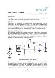
AN ANALOG PREDISTORTION LINEARIZER DESIGN
AN ANALOG PREDISTORTION LINEARIZER DESIGN
AN ANALOG PREDISTORTION LINEARIZER DESIGN

You also want an ePaper? Increase the reach of your titles
YUMPU automatically turns print PDFs into web optimized ePapers that Google loves.
<strong>AN</strong> <strong>AN</strong>ALOG <strong>PREDISTORTION</strong><br />
<strong>LINEARIZER</strong> <strong>DESIGN</strong><br />
In this article, a new type of analog predistortion linearizer is proposed to generate and control<br />
predistorted third and higher order intermodulation signals (IM) separately. By using predistorted<br />
signals, the intermodulation distortion signals generated in power amplifiers can be suppressed<br />
effectively. In order order to validate the proposed approach, a high power amplifier (HPA), using the<br />
proposed predistortion linearizer, has been fabricated to operate in the Korean PCS base station<br />
transmitter band (1840 to 1870 MHz). The test results show that the IMD 3 and IMD 5 of the power<br />
amplifier are improved by more than 40 and 23 dB for CW two-tone signals, respectively. The<br />
predistorter also improves the adjacent channel power ratio (ACPR) by more than 10 dB for CDMA<br />
(IS-95) 4FA signals.<br />
In the past, voice transmission was the<br />
main issue in communications. However,<br />
new requirements have evolved from<br />
voice to data and mobile communications,<br />
which demand a larger amount of information<br />
and better quality. Because of these requirements,<br />
more complex modulation and demodulation<br />
schemes and broadband channel bandwidths<br />
are necessary in modern mobile communications<br />
systems. In general, complex<br />
modulation and demodulation schemes require<br />
linear transmitters and receivers. In<br />
power amplifier design, high linearity, in addition<br />
to high efficiency, is a critical issue.<br />
When signals are amplified in an HPA, unwanted<br />
harmonics and intermodulation distortion<br />
signals are generated, in addition to the<br />
amplified desired signals, by the nonlinear<br />
characteristics of the power amplifier. These<br />
IM signals increase the bit error rate (BER) of<br />
the data and the adjacent channel interferences,<br />
and decrease the power amplifier efficiency.<br />
Predistortion is a linearization tech-<br />
nique that connects a circuit having inverse<br />
distortion characteristics at the input of the<br />
amplifier. Because of the inverse distortion<br />
characteristics, the predistortion linearizer can<br />
reduce the IM signals generated by the HPA. 1<br />
If the third, fifth and higher order IM products<br />
can be generated and controlled separately<br />
in the predistorter, the IM products of<br />
the power amplifier can be reduced more effectively.<br />
2 This method presents a problem<br />
caused by signal interference in small size circuits<br />
and is difficult to implement. In this article,<br />
a new type of analog predistortion lin-<br />
YOUNG KIM<br />
Kumoh National Institute of Technology<br />
Gyungbuk, Korea<br />
IK-SOO CH<strong>AN</strong>G<br />
Sogang University, Seoul, Korea<br />
YONG-CHAE JEONG<br />
Chonbuk National University<br />
Chonju, Korea<br />
Reprinted with permission of MICROWAVE JOURNAL ® from the February 2005 issue.<br />
©<br />
2005 Horizon House Publications, Inc.
TECHNICAL FEATURE<br />
4f 1 −3f 2<br />
2f 1 −f 2 2f 2 −f 1<br />
4f 2 −3f 1<br />
2f 1 −f 2 f 1 f 2 2f 2 −f 1<br />
2f 1 −f 2 f 1 f 2 2f 2 −f 1 3f 1 −2f 2 f 1 f 2 3f 2 −2f 1<br />
RF IN<br />
RF OUT<br />
f 1 f 2<br />
V CC<br />
RF OUT<br />
RF IN<br />
TR<br />
R<br />
C<br />
▲ Fig. 1 Block diagram of the third-order intermodulation signal<br />
generator (IMG 3 ).<br />
earizer is proposed to reduce HPA<br />
nonlinearity by generating and controlling<br />
individual order IM signals.<br />
PREDISTORTER<br />
OPERATING THEORY<br />
The nonlinearity of an amplifier can<br />
be expressed in terms of a power series<br />
v o = k 1 v i + k 2 v i + k 3 v i + k 4 v i … (1)<br />
where<br />
v o = output signal<br />
v i = input signal<br />
If the input signal consists of two<br />
signals of equal amplitude, as<br />
v i = A[cos(ω 1 t) + cos(ω 2 t)] (2)<br />
then the DC, the intermodulation distortion<br />
components (ω 1 ±ω 2 , 2ω 1 –ω 2 ,<br />
2ω 2 –ω 1 , …) and the harmonic components<br />
(2ω 1 , 2ω 2 , 3ω 1 , 3ω 2 ), besides the<br />
desired amplified input signals (ω 1 , ω 2 )<br />
appear at the output port because of<br />
the HPA nonlinear characteristics. The<br />
harmonic generator of the proposed<br />
distorter has a simple structure. Figure<br />
1 shows the block diagram of the thirdorder<br />
intermodulation signal generator<br />
(IMG 3 ). Its output signals obtained<br />
from the IMG 3 are the main and thirdorder<br />
intermodulation signals, given by<br />
H 13 = k 1 v 1 + k 3 v 3 i<br />
H 13 = a 1 cos(ω 1 t) + a 2 cos(ω 2 t)<br />
+ a 3 cos(2ω 1 –ω 2 )t + a 4 cos(2ω 2 –ω 1 )t<br />
+ a 5 cos(3ω 1 t) + a 6 cos(3ω 2 t) (3)<br />
The desired signals (ω 1 , ω 2 , 2ω 1 –ω 2 ,<br />
2ω 2 –ω1) are elements of H 13 as<br />
shown by Equations 1, 2 and 3. The<br />
bias voltage of the small signal transistor<br />
is controlled to generate a<br />
third-order IM signal as large as possible.<br />
An MSA-0386 transistor from<br />
HP is used in the IMG 3 generator.<br />
Figure 2 shows<br />
the block diagram<br />
of the higher order intermodulation<br />
signals generator (IMG h ), which uses<br />
as input the output signals from the<br />
IMG 3 . They are given by the expression<br />
H h = k1H 13 + k 3 H 13 3 + k 5 H 13<br />
5<br />
DIODE<br />
H h = b 1 cos(ω 1 t) + b 2 cos(ω 2 t)<br />
+ b 3 cos(2ω 1 –ω 2 )t + b 4 cos(2ω 2 –ω 1 )t<br />
+ b 5 cos(3ω 1 –2ω 2 )t<br />
+ b 6 cos(3ω 2 –2ω 1 )t<br />
+ b 7 cos(4ω 1 –3ω 2 )t<br />
+ b 8 cos(4ω 2 –3ω 1 )t + … (4)<br />
IMG h consists of a 3 dB hybrid coupler,<br />
two anti-paralleled Shottky diodes<br />
for high order intermodulation signal<br />
AMPLITUDE (10 dB/div)<br />
1.851 1.855 1.859<br />
FREQUENCY (GHz)<br />
▲ Fig. 3 IMG 3 output for CW two-tone<br />
input signals.<br />
AMPLITUDE (10 dB/div)<br />
1.849 1.855 1.863<br />
FREQUENCY (GHz)<br />
▲ Fig. 4 IMG 3 output for CDMA 2FA<br />
input signals.<br />
▲ Fig. 2 Block diagram of the high order intermodulation signal<br />
generator (IMG h ).<br />
generation, and a resistor and capacitor<br />
to control amplitude and phase of the<br />
input signal to generate only the desired<br />
high order IM terms. 3<br />
Figure 3 shows the output of the<br />
IMG 3 for the case of CW two-tone input<br />
signals at 1.854 and 1.855 GHz.<br />
Figure 4 shows the output of the<br />
IMG 3 for the case of CDMA 2FA input<br />
signals at 1853.75 and 1.856.25<br />
MHz. Figures 5 and 6 show the IMG h<br />
output in the case of CW two-tone and<br />
CDMA 2FA signals, respectively.<br />
A power amplifier, using the new<br />
type of analog predistorter to control<br />
the individual order intermodulations,<br />
AMPLITUDE (10 dB/div)<br />
1.851 1.855 1.859<br />
FREQUENCY (GHz)<br />
▲ Fig. 5 IMG h output for CW two-tone<br />
input signals.<br />
AMPLITUDE (10 dB/div)<br />
1.845 1.855 1.865<br />
FREQUENCY (GHz)<br />
▲ Fig. 6 IMG h output for CDMA 2FA<br />
input signals.
TECHNICAL FEATURE<br />
RF IN<br />
ALC<br />
CKT<br />
IMG 3<br />
DELAY<br />
IMG 3<br />
CONTROL<br />
BLOCK<br />
IMG H<br />
Figure 8 shows the ACPR improvements<br />
as a function of input<br />
power level for a CDMA 1FA signal.<br />
Figure 9 compares the carrier to intermodulation<br />
distortion (C/I) ratio of<br />
the HPA with and without the prowas<br />
designed, as shown in Figure 7. It<br />
consists of an automatic level controller<br />
(ALC) circuit, an IMG 3 and<br />
IMG 3 control block, an IMG h and<br />
IMG h control block, and a high power<br />
amplifier (HPA). The input signals are<br />
divided into the HPA and the ALC<br />
paths by a directional coupler. Since<br />
the HPA is usually operated over a<br />
wide dynamic power range, the ALC<br />
generates a constant signal level for effective<br />
predistortion signal generation.<br />
The ALC circuit, at the input port, stabilizes<br />
the device, resulting in a constant<br />
IM signal in spite of the changes<br />
in input power level. Using this constant<br />
ALC output level, IMG 3 and<br />
IMG h generate the third and higher<br />
order IM signals, respectively.<br />
The IMG 3 and IMG h control blocks<br />
consist of a variable attenuator and a<br />
variable phase shifter to control the<br />
magnitude and phase of the third and<br />
higher order inverse IM signals to the<br />
HPA. The delay circuit in the power<br />
amplifier path compensates for the delay<br />
in the IM generators and IM control<br />
circuits. Adaptive control of the<br />
magnitude and phase of the third and<br />
higher IM signals is necessary to match<br />
those of the intermodulation signals<br />
generated by the HPA over the dynamic<br />
power range. 4–6<br />
EXPERIMENTAL RESULTS<br />
In order to show the validity of the<br />
proposed predistorter, a power amplifier<br />
(STA1800-37 from Sewon Teletec<br />
Inc.), employed in base stations and repeaters<br />
of the Korean Personal Communications<br />
Service (KPCS), was used<br />
in the experiment. Its gain and 1 dB<br />
compression power are 50 dB and 37<br />
dBm, respectively. The delay circuit is<br />
realized with a coaxial delay line of 14<br />
ns. The variable attenuators and variable<br />
phase shifters are of the reflection<br />
IMG H<br />
CONTROL<br />
BLOCK<br />
▲ Fig. 7 Block diagram of the new type of analog predistortion power amplifier.<br />
HPA<br />
RF OUT<br />
type in order to obtain good reflection<br />
characteristics. The variable phase<br />
shifter uses a varactor diode 1T362<br />
from Sony and a variable attenuator, a<br />
PIN diode HSMP-4810 from HP.<br />
AMPLITUDE (10 dB/div)<br />
1.85061 1.85461 1.85861<br />
(a)<br />
FREQUENCY (GHz)<br />
AMPLITUDE (10 dB/div)<br />
IMPROVEMENT (dB)<br />
16<br />
14<br />
12<br />
10<br />
8<br />
6<br />
4<br />
2<br />
0<br />
1.25 MHz<br />
2.25 MHz<br />
885 kHz<br />
−6 −7 −8 −9 −10 −11<br />
INPUT POWER (dBm)<br />
▲ Fig. 8 ACPR improvements versus input<br />
power for a CDMA 1FA signal.<br />
1.85061 1.85461 1.85861<br />
(b)<br />
FREQUENCY (GHz)<br />
▲ Fig. 9 C/I characteristics of HPA (a) without and b) with the proposed predistortion<br />
linearizer in the case of a two-tone signal (P O =37.7 dBm/tone).<br />
AMPLITUDE (10 dB/div)<br />
1.8512 1.8550 1.8578 1.8512 1.8550 1.8578<br />
(a) FREQUENCY (GHz) (b) FREQUENCY (GHz)<br />
▲ Fig. 10 ACPR characteristics of the HPA (a) without and b) with the proposed predistortion<br />
linearizer in the case of a CDMA 1FA signal (P O =37.0 dBm).<br />
AMPLITUDE (10 dB/div)<br />
AMPLITUDE (10 dB/div)<br />
1.8490 1.8550 1.8610 1.8490 1.8550 1.8610<br />
(a) FREQUENCY (GHz) (b) FREQUENCY (GHz)<br />
▲ Fig. 11 ACPR characteristics of the HPA (a) without and b) with the proposed predistortion<br />
linearizer in the case of a CDMA 4FA signal (P O =30.0 dBm/FA).<br />
AMPLITUDE (10 dB/div)
posed predistortion circuit for the case<br />
of CW two-tone signals, where the<br />
output power is 37.7 dBm/tone. The<br />
test frequencies are 1.854 and 1.855<br />
GHz. The improvements of IMD 3 and<br />
IMD 5 are 42.87 and 23.95 dB, respectively.<br />
Figure 10 shows the CDMA<br />
1FA adjacent power ratio (ACPR) of<br />
the HPA with and without the proposed<br />
predistortion circuit. The output<br />
power is 37 dBm and the test frequency<br />
is 1.855 GHz. Figure 11 compares<br />
the CDMA 4FA ACPR of the<br />
HPA with and without the proposed<br />
predistortion circuit, where the output<br />
power is 30 dBm/FA and the carrier<br />
frequencies are 1.8525, 1.85375,<br />
1.85625 and 1.8575 GHz, respectively.<br />
The improvements in ACPR are<br />
10.25, 8.6 and 9.37 dB at f 0 ±885 kHz,<br />
f 0 ±1.25 MHz and f 0 ±2.25 MHz, respectively.<br />
The test signal generator is<br />
ESG4433B from Agilent Technologies.<br />
A signal similar to a carrier leakage<br />
was observed at the center frequency<br />
with this equipment.<br />
CONCLUSION<br />
In this article, a new type of analog<br />
predistortion linearizer for controlling<br />
individual intermodulation distortion<br />
signals is proposed. The signal generators<br />
generate and control predistorted<br />
third and higher IM component signals<br />
separately. The high order IM signals<br />
are generated by using the main and<br />
third-order IM signals at the input of<br />
the generator. The proposed predistorter<br />
structure offers the advantage of<br />
little signal interference in small size<br />
circuits and easy implementation. Using<br />
the predistorted signals, the HPA’s<br />
intermodulation distortion signals are<br />
suppressed effectively. The test results<br />
show that IMD 3 and IMD 5 are reduced<br />
by more than 40 and 23 dB for<br />
CW two-tone signals, respectively. The<br />
predistorter improves the ACPR by<br />
more than 10 dB for CDMA<br />
(IS-95) 4FA signals. ■<br />
ACKNOWLEDGMENT<br />
This work was supported by the Research<br />
Fund, Kumoh National Institute<br />
of Technology, Gyungbuk, Korea.<br />
References<br />
1. P.B. Kenington, High Linearity RF Amplifier<br />
Design, Artech House Inc., Norwood,<br />
MA, 2000, pp. 341–420.<br />
2. Y.C. Jeong, “A Design of Predistortion Linearizer<br />
by Individual Order Control of Intermodulation<br />
Distortion Signals,” PhD<br />
Dissertation, Sogang University, 1996.<br />
3. T. Nojima and T. Konno, “Cuber Predistortion<br />
Linearizer for Relay Equipment in<br />
800 MHz Band Land Mobile Telephone<br />
System,” IEEE Transactions on Vehicular<br />
Technology, Vol. 34, No. 4, Nov.1985.<br />
4. S.A. Maas, Nonlinear Microwave Circuits,<br />
Artech House Inc., Norwood, MA, 1988.<br />
5. T.T. Ha, Solid-state Microwave Amplifier<br />
Design, John Wiley & Sons Inc., Somerset,<br />
NJ, 1981.<br />
6. S.C. Cripps, RF Power Amplifiers for<br />
Wireless Communications, Artech House<br />
Inc., Norwood, MA, 1999.<br />
TECHNICAL FEATURE<br />
Young Kim received<br />
his BSEE, MSEE and<br />
PhD degrees in<br />
electronics engineering<br />
from Sogang<br />
University, Seoul,<br />
Korea, in 1986, 1988<br />
and 2002, respectively.<br />
In 2003, he joined the<br />
school of electronics<br />
engineering, Kumoh<br />
National Institute of<br />
Technology, Gumi, Korea. His interests include<br />
the design of high power amplifiers and<br />
linearization techniques, and RF and<br />
microwave circuit analysis and design. He can<br />
be reached via e-mail at youngk@kumoh.ac.kr.<br />
Ik-Soo Chang<br />
received his PhD<br />
degree from Seoul<br />
National University,<br />
Seoul, Korea, in 1982.<br />
He is currently a<br />
professor at Sogang<br />
University. He has<br />
more than 20 years of<br />
experience in RF and<br />
microwave circuit<br />
design.<br />
Yong-Chae Jeong<br />
received his BSEE,<br />
MSEE and PhD degrees<br />
in electronics<br />
engineering from<br />
Sogang University,<br />
Seoul, Korea, in 1989,<br />
1991 and 1996,<br />
respectively. In 1998, he<br />
joined the division of<br />
electronics and<br />
information engineering<br />
at the Institute of Information and<br />
Communication at Chonbuk National University,<br />
Chonju, Korea. He is currently an associate<br />
professor and chair of the Chonbuk University<br />
IC Design Education Center (IDEC) WG, where<br />
he teaches and conducts research in the areas of<br />
microwave devices, base station amplifiers,<br />
nonlinear devices and system linearizing<br />
technology, and RFIC design.