
Create successful ePaper yourself
Turn your PDF publications into a flip-book with our unique Google optimized e-Paper software.
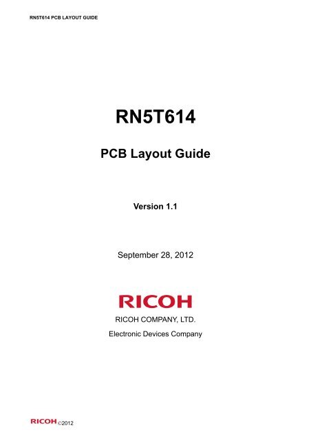
<strong>RN5T614</strong> <strong>PCB</strong> <strong>LAYOUT</strong> <strong>GUIDE</strong><br />
<strong>RN5T614</strong><br />
<strong>PCB</strong> Layout Guide<br />
Version 1.1<br />
September 28, 2012<br />
RICOH COMPANY, LTD.<br />
Electronic Devices Company<br />
©2012
<strong>RN5T614</strong> <strong>PCB</strong> <strong>LAYOUT</strong> <strong>GUIDE</strong><br />
Abstract<br />
This document describes the constraints and points when designing the <strong>PCB</strong> layout with <strong>RN5T614</strong>.<br />
This guide provides examples to explain of how it can be done.<br />
The <strong>PCB</strong> layout example is helpful to achieve optimal <strong>RN5T614</strong> performance.<br />
Contents<br />
1. Basic Policy and Examples of Board Pattern ............................................................................................. 3<br />
1.1 .................................................................................................................................... 3<br />
1.2 .................................................................................................................................. 6<br />
2. Recommended External Parts List ............................................................................................................. 7<br />
3. Example of Parts Layout............................................................................................................................. 8<br />
©2012 Page 2
<strong>RN5T614</strong> <strong>PCB</strong> <strong>LAYOUT</strong> <strong>GUIDE</strong><br />
1. Basic Policy and Examples of Board Pattern<br />
1.1 <br />
Current Loop<br />
Cin_A<br />
Analog<br />
Power<br />
Supply<br />
<strong>RN5T614</strong><br />
Buffer<br />
Power<br />
Supply<br />
Cin_B<br />
(Input capacitance)<br />
VFB<br />
Control<br />
and<br />
Analog<br />
BUF<br />
LX<br />
L<br />
Vout<br />
Cout<br />
(Output capacitance)<br />
Analog<br />
GND<br />
Buffer<br />
GND<br />
Fig. 1-1: Simplified Schematic for DCDC1 and DCDC2<br />
Analog<br />
Power<br />
Supply<br />
<strong>RN5T614</strong><br />
Buffer<br />
Power<br />
Supply<br />
Current Loop<br />
Cin_A<br />
Cin_B<br />
(Input capacitance)<br />
Control<br />
and<br />
Analog<br />
BUF<br />
LX<br />
R1<br />
L<br />
Cf<br />
Vout<br />
Cout<br />
(Output capacitance)<br />
+<br />
- VREF<br />
VFB<br />
R2<br />
Analog<br />
GND<br />
Buffer<br />
GND<br />
Fig. 1-2: Simplified Schematic for DCDC3<br />
©2012 Page 3
<strong>RN5T614</strong> <strong>PCB</strong> <strong>LAYOUT</strong> <strong>GUIDE</strong><br />
<strong>RN5T614</strong> Pin Names<br />
DCDC1 DCDC2 DCDC3<br />
Analog Power Supply<br />
VINA<br />
Buffer Power Supply VINP1 VINP2 VINP3<br />
VFB VFB1 VFB2 VFB3<br />
LX LX1 LX2 LX3<br />
Table 1-1: <strong>RN5T614</strong> Pin Names<br />
(7)<br />
(8)<br />
(3)<br />
C<br />
L<br />
(1)<br />
(4)<br />
(5)<br />
(6)<br />
(5)<br />
(1)<br />
(4)<br />
LX<br />
L<br />
C<br />
VOUT<br />
(2)<br />
(7)<br />
(3)<br />
Fig. 1-3: DCDC Block Evaluation Board Pattern (Top Layer)<br />
(1) Place the parts to minimize the switching current loop (Figure 1-1 and 1-2: blue line, Figure 1-3: red<br />
line).<br />
(2) Route the LX line between <strong>RN5T614</strong> and an inductor as short and wide as possible,<br />
and yet should not add other redundant lines on it<br />
(3) Connect the GND line of “Cout” directly to the internal GND plane with multiple vias, in order to reduce<br />
impedance as small as possible. (Target: 50mΩ or less)<br />
(4) Begin to route the VOUT line from near not “L” but “Cout”.<br />
(5) Place “Cin” as close as possible to <strong>RN5T614</strong>. (Higher priority level is “Cin” < L < “Cout” in the close<br />
distance order with <strong>RN5T614</strong>.)<br />
©2012 Page 4
<strong>RN5T614</strong> <strong>PCB</strong> <strong>LAYOUT</strong> <strong>GUIDE</strong><br />
(7)<br />
VFB3<br />
VFB1<br />
(7)<br />
Fig. 1-4: DCDC Block Evaluation Board Pattern<br />
*Top Layer (High-light: Lx and VOUT) + 3rd Layer (VFB)<br />
(6) Place inductors for DCDC1, DCDC2 and DCDC3 without becoming too close between them, in order to<br />
avoid the electromagnetic interference.<br />
(7) Route the VFB line not to go back into the chip parallel to noise source as the LX line in the same layer,<br />
and it's preferable to set the VFB line in the different layer from noise source.<br />
In addition, it should not pass under the Inductors.<br />
(8) Place R1, R2, and Cf as close as possible in the same layer, and connect GND of R2 to Cout's in<br />
DCDC3.<br />
Note:<br />
*Need to arrange the layout pattern of DCDC2 along with DCDC1's, too. (Pay attention to (6) at that time.)<br />
©2012 Page 5
<strong>RN5T614</strong> <strong>PCB</strong> <strong>LAYOUT</strong> <strong>GUIDE</strong><br />
1.2 <br />
IMONI<br />
(1)<br />
VCHG<br />
VBAT<br />
VSYS<br />
(2)<br />
Fig. 1-5: Charger Block Evaluation Board Pattern (Top Layer)<br />
(1) Place each capacitor (VCHG, VSYS*, VBAT*) as close as possible to <strong>RN5T614</strong> and route the line to<br />
<strong>RN5T614</strong> short and widely in order to minimize resistance.<br />
(2) Place IMONI resistance as close as possible to <strong>RN5T614</strong> and route the line of it to avoid the having<br />
many parasitic resistance. And Use the high-accuracy resistance (Recommended value: ±0.5% or less)<br />
in order to increase the accuracy of Charge Current.<br />
(3) The device can withstand up to 6.5V on VCHG pin. However, it can withstand high voltage by combining a<br />
high voltage protection IC (up to 28V by using BD6040 of ROHM)<br />
©2012 Page 6
<strong>RN5T614</strong> <strong>PCB</strong> <strong>LAYOUT</strong> <strong>GUIDE</strong><br />
2. Recommended External Parts List<br />
<strong>RN5T614</strong> External Parts<br />
Block Pin Name<br />
Parts Size [mm]<br />
Parts<br />
Model value Vender Num<br />
X Size Y Size Z Size [mm2]<br />
PMU - - <strong>RN5T614</strong> RICOH 1 6.00 6.00 0.90 36<br />
CHG VCHG 4.7uF GRM21BB31E475KA75B Murata 1 2.00 1.25 1.25 2.5<br />
Zener Diode RD6.8UM RENESAS 1 2.10 0.80 0.70 1.68<br />
(for OVP) OVP BD6040 ROHM 1 1.60 1.60 0.55 2.56<br />
2.2uF GRM188B31C225KE14B Murata 1 1.60 0.80 0.80 1.28<br />
VSYS1 10uF C1608JB0J106M TDK 1 1.60 0.80 0.80 1.28<br />
VSYS2<br />
VSYS3<br />
VBAT1 4.7uF GRM188B30J475KE18B Murata 1 1.60 0.80 0.80 1.28<br />
VBAT2<br />
THERMBAT Thermistor NTCG103JF103GT TDK 1 1.00 0.50 0.50 0.5<br />
10kohm - 1 1.00 0.50 0.35 0.5<br />
VTHM 1.0uF GRM155B31A105KE15 Murata 1 1.00 0.50 0.50 0.5<br />
IMONI 1kohm 1kohm +/- 0.5% - 1 1.00 0.50 0.35 0.5<br />
VCHGREG 1.0uF GRM155B31A105KE15 Murata 1 1.00 0.50 0.50 0.5<br />
DCDC VINA 2.2uF LMK107BJ225KA Taiyo Yuden 1 1.60 0.80 0.80 1.28<br />
VINP1 2.2uF LMK107BJ225KA Taiyo Yuden 1 1.60 0.80 0.80 1.28<br />
LX1 2.2uH NRH2410T2R2MN Taiyo Yuden 1 2.40 2.40 1.00 5.76<br />
VFB1 10uF C1608JB0J106M TDK 1 1.60 0.80 0.80 1.28<br />
VINP2 10uF LMK107BBJ106MALT Taiyo Yuden 1 1.60 0.80 0.80 1.28<br />
LX2 2.2uH NRH2410T2R2MN Taiyo Yuden 1 2.40 2.40 1.00 5.76<br />
VFB2 10uF C1608JB0J106M TDK 1 1.60 0.80 0.80 1.28<br />
VINP3 2.2uF LMK107BJ225KA Taiyo Yuden 1 1.60 0.80 0.80 1.28<br />
LX3 2.2uH MLP2012S2R2M TDK 1 2.00 1.25 1.00 2.5<br />
VFB3 4.7uF C1608JB1A475K TDK 1 1.60 0.80 0.80 1.28<br />
R1 (for DCDC3 Voltage set) - 1 1.00 0.50 0.35 0.5<br />
R2 (for DCDC3 Voltage set) - 1 1.00 0.50 0.35 0.5<br />
Cf (for DCDC3 Voltage set) - 1 1.00 0.50 0.50 0.5<br />
LDO VIN1 1.0uF GRM155B31A105KE15 Murata 1 1.00 0.50 0.50 0.5<br />
VREF 1.0uF GRM155B31A105KE15 Murata 1 1.00 0.50 0.50 0.5<br />
VOUT1 1.0uF GRM155B31A105KE15 Murata 1 1.00 0.50 0.50 0.5<br />
VOUT2 1.0uF GRM155B31A105KE15 Murata 1 1.00 0.50 0.50 0.5<br />
VOUT3 1.0uF GRM155B31A105KE15 Murata 1 1.00 0.50 0.50 0.5<br />
VOUT4 1.0uF GRM155B31A105KE15 Murata 1 1.00 0.50 0.50 0.5<br />
VOUTD 1.0uF GRM155B31A105KE15 Murata 1 1.00 0.50 0.50 0.5<br />
VIN2 1.0uF GRM155B31A105KE15 Murata 1 1.00 0.50 0.50 0.5<br />
VOUT5 1.0uF GRM155B31A105KE15 Murata 1 1.00 0.50 0.50 0.5<br />
VOUT6 1.0uF GRM155B31A105KE15 Murata 1 1.00 0.50 0.50 0.5<br />
VIN3 1.0uF GRM155B31A105KE15 Murata 1 1.00 0.50 0.50 0.5<br />
VOUT7 1.0uF GRM155B31A105KE15 Murata 1 1.00 0.50 0.50 0.5<br />
VOUT8 1.0uF GRM155B31A105KE15 Murata 1 1.00 0.50 0.50 0.5<br />
OTHER VDDIO 0.1uF GRM155B31A105KE15 Murata 1 1.00 0.50 0.50 0.5<br />
BATDET 330kohm for Pullup - 1 1.00 0.50 0.35 0.5<br />
ONOB 330kohm for Pullup - 1 1.00 0.50 0.35 0.5<br />
RESETO 330kohm for Pullup - 1 1.00 0.50 0.35 0.5<br />
SDA 330kohm for Pullup - 1 1.00 0.50 0.35 0.5<br />
INTB 330kohm for Pullup - 1 1.00 0.50 0.35 0.5<br />
Total Num 44 Total Parts size 83.06<br />
©2012 Page 7
<strong>RN5T614</strong> <strong>PCB</strong> <strong>LAYOUT</strong> <strong>GUIDE</strong><br />
3. Example of Parts Layout<br />
8.1 mm<br />
4.5 mm<br />
R<br />
2.3 mm<br />
C<br />
C<br />
R<br />
C<br />
C<br />
R<br />
R<br />
C<br />
R<br />
R<br />
L<br />
C<br />
C<br />
8.5 mm<br />
3.2 mm<br />
C<br />
BD60<br />
40<br />
GUL<br />
D<br />
C<br />
C<br />
C<br />
<strong>RN5T614</strong><br />
C<br />
L<br />
C<br />
11.6 mm<br />
10.5 mm<br />
C C<br />
C<br />
C<br />
C<br />
C<br />
C<br />
L<br />
C<br />
R<br />
R<br />
R<br />
C<br />
C<br />
C<br />
C<br />
C<br />
C<br />
C<br />
1.6 mm<br />
Total Parts Area 158.21mm 2<br />
Fig. 3-1: Example <strong>PCB</strong> Parts Layout<br />
Note: Connect Exposed Paddle (Tab on the bottom side) to GND.<br />
©2012 Page 8