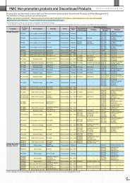
RC5T583S PCB LAYOUT GUIDE - Ricoh
RC5T583S PCB LAYOUT GUIDE - Ricoh
RC5T583S PCB LAYOUT GUIDE - Ricoh

Create successful ePaper yourself
Turn your PDF publications into a flip-book with our unique Google optimized e-Paper software.
<strong>RC5T583S</strong> <strong>PCB</strong> <strong>LAYOUT</strong> <strong>GUIDE</strong><br />
<strong>RC5T583S</strong><br />
<strong>PCB</strong> Layout Guide<br />
Version 1.0<br />
September 28, 2012<br />
RICOH COMPANY, LTD.<br />
Electronic Devices Company<br />
©2012
<strong>RC5T583S</strong> <strong>PCB</strong> <strong>LAYOUT</strong> <strong>GUIDE</strong><br />
Abstract<br />
This document describes the constraints and points when designing the <strong>PCB</strong> layout with <strong>RC5T583S</strong>.<br />
This guide provides examples to explain of how it can be done.<br />
The <strong>PCB</strong> layout example is helpful to achieve optimal <strong>RC5T583S</strong> performance.<br />
Contents<br />
1. Basic Policy and Examples of Board Pattern ............................................................................................. 3<br />
1.1 ................................................................................................................................. 3<br />
1.1.1 DCDC1, DCDC2 and DCDC3 .....................................................................................................................3<br />
1.1.2 DCDC0 (High current type) .........................................................................................................................8<br />
1.2 RTC Block...................................................................................................................................... 12<br />
2. Recommended External Parts List (*Maximum height: 3.0mm)......................................................... 14<br />
3 Parts Place Example ......................................................................................................................... 15<br />
©2012 Page 2
<strong>RC5T583S</strong> <strong>PCB</strong> <strong>LAYOUT</strong> <strong>GUIDE</strong><br />
1. Basic Policy and Examples of Board Pattern<br />
1.1 <br />
1.1.1 DCDC1, DCDC2 and DCDC3<br />
Current Loop<br />
Cin_A<br />
Analog<br />
Power<br />
Supply<br />
RCT583S<br />
Buffer<br />
Power<br />
Supply<br />
Cin_B<br />
(Input capacitance)<br />
VFB<br />
Control<br />
and<br />
Analog<br />
BUF<br />
LX<br />
L<br />
Vout<br />
Cout<br />
(Output capacitance)<br />
Analog<br />
GND<br />
Buffer<br />
GND<br />
Fig.1-1 Simplified Schematic for DCDC<br />
DCDC1 DCDC2 DCDC3<br />
Analog Power Supply<br />
VIN3<br />
Buffer Power Supply VIN2, 5 VIN4 VIN6, 7<br />
Buffer GND GND 2, 3 GND 4, 5 GND 6, 7<br />
Analog GND<br />
GND8<br />
VFB FB1 FB2 FB3<br />
LX LX11, 12 LX21, 22 LX31, 32<br />
Table1-1: <strong>RC5T583S</strong> Pin Names<br />
©2012 Page 3
<strong>RC5T583S</strong> <strong>PCB</strong> <strong>LAYOUT</strong> <strong>GUIDE</strong><br />
(4)<br />
(1)<br />
Vout<br />
Cout<br />
L<br />
(3)<br />
(2)<br />
LX<br />
(5)<br />
(5)<br />
Fig.1-2 DCDC Block Evaluation Board Pattern (Top Layer)<br />
(1) Place the parts to minimize the switching current loop (Figure 1-1: blue line, Figure 1-2: red line).<br />
(2) Route the LX line as short and wide as possible between <strong>RC5T583S</strong> and an inductor and prohibit<br />
adding other redundant lines to the LX line.<br />
(3) Connect the GND line of “Cout” directly to the internal GND plane with multiple vias, in order to reduce<br />
impedance as small as possible. (Target: 50mΩ or less)<br />
(4) Begin to route the VOUT line from near not “L” but “Cout”.<br />
(5) Place inductors for neighboring DCDC without becoming too close between them, in order to avoid the<br />
electromagnetic interference.<br />
©2012 Page 4
<strong>RC5T583S</strong> <strong>PCB</strong> <strong>LAYOUT</strong> <strong>GUIDE</strong><br />
Vout<br />
Cout<br />
L<br />
VFB<br />
LX<br />
(6)<br />
Fig.1-3: DCDC Block Evaluation Board Pattern (Top Layer (Lx) + 3rd Layer (VFB))<br />
(6) Route the VFB line not to become in parallel with lines, which may be a source of noise, such as the LX<br />
line. If possible, route the VGB line at other layer.<br />
©2012 Page 5
<strong>RC5T583S</strong> <strong>PCB</strong> <strong>LAYOUT</strong> <strong>GUIDE</strong><br />
(8)<br />
Analog GND<br />
(7)<br />
Buffer GND<br />
Fig.1-4: DCDC Block Evaluation Board Pattern (6th Layer)<br />
(7) Provide the ground plane for Analog-GND and Buffer-GND to the inner layer and multiple vias, in order<br />
to minimize impedance.<br />
(8) Divide Analog-GND from Buffer-GND in order to give impedance and avoid mutual interference.<br />
©2012 Page 6
<strong>RC5T583S</strong> <strong>PCB</strong> <strong>LAYOUT</strong> <strong>GUIDE</strong><br />
Buffer power supply<br />
(9)<br />
Cin_B<br />
Fig.1-5: DCDC Block Evaluation Board Pattern (5th Layer (Vin_b) + Bottom Layer (Cin_b))<br />
(9) Place “Cin” as close as possible to <strong>RC5T583S</strong>. (Higher priority level is “Cin” < L < “Cout” in the close<br />
distance order with <strong>RC5T583S</strong>)<br />
In the case of the “Cin” as one example; Place “Cin” on the underside, in order to close to <strong>RC5T583S</strong>.<br />
©2012 Page 7
<strong>RC5T583S</strong> <strong>PCB</strong> <strong>LAYOUT</strong> <strong>GUIDE</strong><br />
1.1.2 DCDC0 (High current type)<br />
less than 5mΩ<br />
Analog<br />
Power<br />
Supply<br />
Buffer<br />
Power<br />
Supply<br />
VIN0<br />
Cin_A<br />
FBP<br />
RCT583S<br />
Control<br />
and BUF<br />
Analog<br />
LH0<br />
LL0<br />
Cin_B1<br />
LX<br />
Cin_B2<br />
L<br />
Vout<br />
Cout<br />
RSO0<br />
FBM<br />
Analog<br />
GND<br />
Buffer<br />
GND<br />
less than 5mΩ<br />
GND0<br />
Fig.1-6: Simplified Schematic for DCDC0<br />
©2012 Page 8
<strong>RC5T583S</strong> <strong>PCB</strong> <strong>LAYOUT</strong> <strong>GUIDE</strong><br />
VIN0 GND VOUT<br />
(1) (1)<br />
(2)<br />
FET<br />
(N)<br />
L<br />
FET<br />
(P)<br />
LX<br />
RSCO0<br />
Fig.1-7: Peripheral DCDC0 Evaluation Board Pattern 1 <br />
(1) Route the power supply for FET and GND at the lower resistance (<strong>RC5T583S</strong>: 5mΩ or less,<br />
Figure 1-6: Blue line).<br />
(2) Place the bypass capacitor of VIN0 for external FET as close as possible to the external FET.<br />
©2012 Page 9
<strong>RC5T583S</strong> <strong>PCB</strong> <strong>LAYOUT</strong> <strong>GUIDE</strong><br />
VIN0 GND VOUT<br />
LL0<br />
L<br />
LX<br />
FBP<br />
(4)<br />
LH0<br />
(3)<br />
Fig.1-8: Peripheral DCDC0 Evaluation Board Pattern 2 <br />
(3) Route the LH0/LL0 gate signal lines to FET to become the low resistance and not to become in parallel<br />
with a source of noise, such as a LX line.<br />
In the case of the LX line as one example; Connect the Lx line to FET at the 8 th layer of the evaluation<br />
board.<br />
(4) Route the VFB (FBP) line not to become in parallel with the LX line and under the coil pattern.<br />
In the case of the VFB line as one example; Route the VFB line for a feedback from output at the 5 th layer<br />
of the evaluation board.<br />
©2012 Page 10
<strong>RC5T583S</strong> <strong>PCB</strong> <strong>LAYOUT</strong> <strong>GUIDE</strong><br />
VIN0<br />
(5)<br />
Fig.1-9: Peripheral DCDC0 Evaluation Board Pattern 3 <br />
(5) Place a bypass capacitor as close as possible to the power supply pin (VIN0) for the internal buffer.<br />
©2012 Page 11
<strong>RC5T583S</strong> <strong>PCB</strong> <strong>LAYOUT</strong> <strong>GUIDE</strong><br />
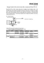
1.2 RTC Block<br />
XIN<br />
<strong>RC5T583S</strong><br />
XOUT<br />
Rd<br />
X'tal<br />
Rx<br />
C<br />
1<br />
C2<br />
Fig.1-10: Simplified Schematic around crystal<br />
(1)<br />
(3)<br />
(2)<br />
(4)<br />
Fig.1-11: Evaluation board pattern example. (Top Layer)<br />
©2012 Page 12
<strong>RC5T583S</strong> <strong>PCB</strong> <strong>LAYOUT</strong> <strong>GUIDE</strong><br />
(1) Place the crystal unit as close as possible to the <strong>RC5T583S</strong>, the route the line on the single layer without<br />
via as short as possible, and not add a redundant line like Monitoring Line.<br />
(2) Place the input and output capacitors (C1 and C2 shown in Fig.1-11) as close as possible to the crystal<br />
unit, in order to reduce the extra parasitic resistance and capacitance.<br />
(3) Draw Land Patterns for Rx and Rd previously, because an adjustment by adding Rx and Rd is required<br />
when the using oscillator exceeds its "Drive Level" specs.<br />
(4) Connect the GND of the oscillation circuit with special GND plane on the component layer (Refer to the<br />
Fig.1-11), and then connect with the internal GND plane by via or through hole. (Refer to the Fig.1-12)<br />
Don’t route the sensitive line on the layer just under the oscillation circuit.<br />
Also, do not place GND between pads of the oscillator to prevent a parasitic resistance.<br />
(4)<br />
Fig.1-12: Evaluation board pattern example (2nd Layer)<br />
©2012 Page 13
<strong>RC5T583S</strong> <strong>PCB</strong> <strong>LAYOUT</strong> <strong>GUIDE</strong><br />
2. Recommended External Parts List<br />
(*Maximum height: 3.0mm)<br />
<strong>RC5T583S</strong> External Parts<br />
Block Pin Name<br />
Parts Size [mm]<br />
Parts<br />
Model No<br />
Vender Num<br />
X Size Y Size Z Size [mm2]<br />
PMU - - <strong>RC5T583S</strong> RICOH 1 5.00 5.00 1.00 25.00<br />
VBAT 1uF GRM155B31A105KE15 Murata 1 1.00 0.50 0.50 0.50<br />
Power VDDIO 0.1uF C0603JB0J104K TDK 1 0.60 0.30 0.30 0.18<br />
VDDGP 0.1uF C0603JB0J104K TDK 1 0.60 0.30 0.30 0.18<br />
ADC ADCVDD 0.1uF C0603JB0J104K TDK 1 0.60 0.30 0.30 0.18<br />
VSB<br />
1kohm P-RMC1/20-102FPA KAMAYA 1 0.60 0.30 0.23 0.18<br />
1uF GRM155B31A105KE15 Murata 1 1.00 0.50 0.50 0.50<br />
RTC<br />
32K X'tal Q13FC135(32.768kHz, 9pF) EPSON 1 3.20 1.50 0.90 4.80<br />
XOUT<br />
13pF Anything - 1 0.60 0.30 0.30 0.18<br />
XIN 13pF Anything - 1 0.60 0.30 0.30 0.18<br />
VIN0<br />
47uF C2012X5R0J476M TDK 2 2.00 1.20 1.25 4.80<br />
2.2uF C1608X5R1A225K TDK 1 1.60 0.80 0.80 1.28<br />
DCDC0<br />
LH0 P-MOS CSD25401Q3 TI 1 3.30 3.30 1.00 10.89<br />
LL0 N-MOS FDMA410NZ Fairchild 1 2.00 2.00 0.80 4.00<br />
FBP 2.2uH SPM6530T-2R2M TDK 1 7.10 6.50 3.00 46.15<br />
FBM 100uF AMK316ABJ107ML Taiyo Yuden 3 3.20 1.60 1.60 15.36<br />
VIN2,VIN5 22uF GRM21BB30J226ME38 Murata 1 2.00 1.25 1.25 2.50<br />
DCDC1 LX11,LX12 2.2uH LTF5022T-2R2N3R2-LC TDK 1 5.00 5.20 2.20 26.00<br />
FB1 47uF C2012X5R0J476M TDK 1 2.00 1.20 1.25 2.40<br />
VIN4 10uF GRM21BB31A106KE18 Murata 1 2.00 1.25 1.25 2.50<br />
DCDC2 LX21,LX22 2.2uH VLS252015ET-2R2M TDK 1 2.50 2.00 1.50 5.00<br />
FB2 22uF AMK107BJ226MA Taiyo Yuden 1 1.60 0.80 0.80 1.28<br />
VIN6,VIN7 22uF GRM21BB30J226ME38 Murata 1 2.00 1.25 1.25 2.50<br />
DCDC3 LX31,LX32 2.2uH VLF5014ST-2R2M2R3 TDK 1 4.80 4.60 1.40 22.08<br />
FB3 47uF C2012X5R0J476M TDK 1 2.00 1.20 1.25 2.40<br />
VIN8 1uF GRM155B31A105KE15 Murata 1 1.00 0.50 0.50 0.50<br />
VIN9 1uF GRM155B31A105KE15 Murata 1 1.00 0.50 0.50 0.50<br />
VIN10 1uF GRM155B31A105KE15 Murata 1 1.00 0.50 0.50 0.50<br />
VIN11 1uF GRM155B31A105KE15 Murata 1 1.00 0.50 0.50 0.50<br />
VO0 1uF GRM155B31A105KE15 Murata 1 1.00 0.50 0.50 0.50<br />
VO1 1uF GRM155B31A105KE15 Murata 1 1.00 0.50 0.50 0.50<br />
VO2 1uF GRM155B31A105KE15 Murata 1 1.00 0.50 0.50 0.50<br />
LDO<br />
VO3 4.7uF JMK105BBJ475MV-F Taiyo Yuden 1 1.00 0.50 0.50 0.50<br />
VO4 1uF GRM155B31A105KE15 Murata 1 1.00 0.50 0.50 0.50<br />
VO5 1uF GRM155B31A105KE15 Murata 1 1.00 0.50 0.50 0.50<br />
VO6 1uF GRM155B31A105KE15 Murata 1 1.00 0.50 0.50 0.50<br />
VO7 4.7uF JMK105BBJ475MV-F Taiyo Yuden 1 1.00 0.50 0.50 0.50<br />
VO8 4.7uF JMK105BBJ475MV-F Taiyo Yuden 1 1.00 0.50 0.50 0.50<br />
VO9 1uF GRM155B31A105KE15 Murata 1 1.00 0.50 0.50 0.50<br />
REG18V 1uF GRM155B31A105KE15 Murata 1 1.00 0.50 0.50 0.50<br />
REFO 1uF GRM155B31A105KE15 Murata 1 1.00 0.50 0.50 0.50<br />
TOTAL 189<br />
Table2-1: External Parts list<br />
©2012 Page 14
<strong>RC5T583S</strong> <strong>PCB</strong> <strong>LAYOUT</strong> <strong>GUIDE</strong><br />
<br />
Size IDC1(A) IDC2(A) DCR(mΩ) IOUTMAX<br />
Item Maker L(mm) W(mm) T(mm) S(mm2) Typ typ typ Total (A)<br />
SPM6530 TDK 7.1 6.5 3 46.15 8.4 8.2 17.3 17 9<br />
SPM4012(1.0uH)×2 TDK 4.4 4.1 1.2 36.08 6 4.1 38 76 4<br />
DCDC0 IHLP2525AHER(1.0uH+0.47u Vishay 6.47 6.86 1.8 88.77 14 7 17.5 26 11<br />
IHLP2525AHER(1.0uH)×2 Vishay 6.47 6.86 1.8 88.77 14 7 17.5 35 11<br />
IHLP2525AHER(0.47uH)×4 Vishay 6.47 6.86 1.8 177.54 18 11 8.4 34 20(AC)<br />
LTF5022T-2R2N3R2-LC TDK 5 5.2 2.2 26.00 3.2 2.4 36 36 3<br />
DCDC1 SPM4012T-2R2M TDK 4.4 4.1 1.2 18.04 4.4 2.7 82 82 3<br />
DFE252012C TOKO 2.5 2 1.2 5.00 2.7 2.3 90 90 3<br />
VLS252012MN-2R2M TDK 2.5 2 1.2 5.00 1.7 1.6 96 96 1.2<br />
DCDC2 SPM4012T-2R2M TDK 4.4 4.1 1.2 18.04 4.4 2.7 82 82 1.2<br />
DFE252012C TOKO 2.5 2 1.2 5.00 2.7 2.3 90 90 1.2<br />
VLF5014ST-2R2M2R3 TDK 4.8 4.6 1.4 22.08 3 2.3 59 59 2<br />
DCDC3 SPM4012T-2R2M TDK 4.4 4.1 1.2 18.04 4.4 2.7 82 82 2<br />
DFE252012C TOKO 2.5 2 1.2 5.00 2.7 2.3 90 90 2<br />
Table2-2: External Parts list<br />
*IDC1…-30% Reduction from Normal L Value<br />
*IDC2…self temperature rise(+40degC typ).<br />
The following are guidelines to the select the inductor.<br />
・"IDC1" is larger than Max Current(DC).<br />
・It is better that "IDC2" is over the Max Current.<br />
-> It is necessary to care the increasing temperature if load current is over IDC2.<br />
・It is better that "DCR" is small.<br />
-> In case of serial connection, the efficiency is dropping because DCR is increase.<br />
3 Parts Place Example<br />
This layout is one example of parts layout with <strong>RC5T583S</strong><br />
20.5 mm<br />
L<br />
L<br />
7 mm<br />
p-mos<br />
C<br />
C<br />
C<br />
C<br />
C<br />
C<br />
C<br />
C<br />
L<br />
C<br />
n-<br />
mos<br />
C<br />
C<br />
C<br />
C<br />
11.2 mm<br />
17.5 mm<br />
<strong>RC5T583S</strong><br />
L<br />
Xtal<br />
L<br />
3.4 mm<br />
12.1 mm<br />
5.1 mm<br />
*PKG: BGA 5.0mm×5.0mm、0.5mmpitch、81pins<br />
Fig3-1: Example of parts place<br />
©2012 Page 15