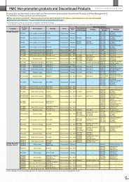
For Printing (7 pages/525KB) - Ricoh
For Printing (7 pages/525KB) - Ricoh
For Printing (7 pages/525KB) - Ricoh

You also want an ePaper? Increase the reach of your titles
YUMPU automatically turns print PDFs into web optimized ePapers that Google loves.
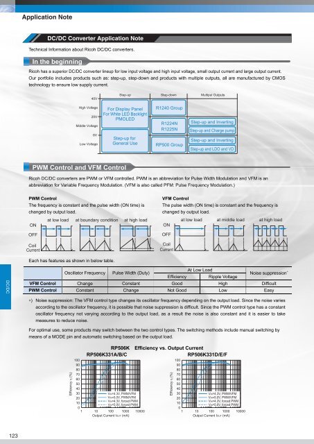
Application Note<br />
DC/DC Converter Application Note<br />
Technical Information about <strong>Ricoh</strong> DC/DC converters.<br />
In the beginning<br />
<strong>Ricoh</strong> has a superior DC/DC converter lineup for low input voltage and high input voltage, small output current and large output current.<br />
Our portfolio includes products such as: step-up, step-down and products with multiple outputs, all are manufactured by CMOS<br />
technology to ensure low supply current.<br />
40V<br />
Step-up<br />
Step-down<br />
Multipul Outputs<br />
High Voltage<br />
20V<br />
Middle Voltage<br />
6V<br />
Low Voltage<br />
<strong>For</strong> Display Panel<br />
<strong>For</strong> White LED Backlight<br />
PMOLED<br />
Step-up for<br />
General Use<br />
R1240 Group<br />
R1224N<br />
R1225N<br />
RP500 Group<br />
Step-up and Inverting<br />
Step-up and Charge pump<br />
Step-up and Inverting<br />
Step-up and LDO and VD<br />
PWM Control and VFM Control<br />
<strong>Ricoh</strong> DC/DC converters are PWM or VFM controlled. PWM is an abbreviation for Pulse Width Modulation and VFM is an<br />
abbreviation for Variable Frequency Modulation. (VFM is also called PFM: Pulse Frequency Modulation.)<br />
PWM Control<br />
The frequency is constant and the pulse width (ON time) is<br />
changed by output load.<br />
ON<br />
OFF<br />
Coil<br />
Current<br />
at low load at boundary condition at high load<br />
VFM Control<br />
The pulse width (ON time) is constant and the frequency is<br />
changed by output load.<br />
ON<br />
OFF<br />
Coil<br />
Current<br />
at low load at middle load at high load<br />
Each has features as shown in below table.<br />
DC/DC<br />
Oscillator Frequency Pulse Width (Duty)<br />
At Low Load<br />
Efficiency Ripple Voltage<br />
Noise suppression ∗<br />
VFM Control Change Constant Good High Difficult<br />
PWM Control Constant Change Not Good Low Easy<br />
∗) Noise suppression: The VFM control type changes its oscillator frequency depending on the output load. Since the noise varies<br />
according to the oscillator frequency, it is possible that noise suppression is difficult. Since the PWM control type has a constant<br />
oscillator frequency not varying according to the output load, as a result the noise is also constant and it is easier to take<br />
measures to reduce noise.<br />
<strong>For</strong> optimal use, some products may switch between the two control types. The switching methods include manual switching by<br />
means of a MODE pin and automatic switching based on the output load.<br />
Efficiency (%)<br />
RP506K Efficiency vs. Output Current<br />
RP506K331A/B/C<br />
RP506K331D/E/F<br />
100<br />
90<br />
80<br />
70<br />
60<br />
50<br />
40<br />
30<br />
VIN=4.3V, PWM/VFM<br />
20<br />
VIN=5.0V, PWM/VFM<br />
VIN=4.3V, forced PWM<br />
10<br />
VIN=5.0V, forced PWM<br />
0<br />
1 10 100 1000 10000<br />
Output Current IOUT (mA)<br />
Efficiency (%)<br />
100<br />
90<br />
80<br />
70<br />
60<br />
50<br />
40<br />
30<br />
VIN=4.3V, PWM/VFM<br />
20<br />
VIN=5.0V, PWM/VFM<br />
VIN=4.3V, forced PWM<br />
10<br />
VIN=5.0V, forced PWM<br />
0<br />
1 10 100 1000 10000<br />
Output Current IOUT (mA)<br />
123
A p p l i c a t i o n N o t e<br />
Internal or External Output Driver Transistor<br />
<strong>Ricoh</strong> has DC/DC converter types available with an internal output transistor and external output transistor. In internal types have<br />
an Lx pin and are called DC/DC converters, the external types have an EXT pin and are called DC/DC controllers. (If a specific<br />
product has both types available it is listed as a DC/DC converter)<br />
When using an external output transistor, select a power MOSFET. When efficiency at high loads is important select a MOSFET<br />
with a low ON resistance, but when efficiency at a low loads is more important select a MOSFET with small gate capacity. Please<br />
use a MOSFET that has a maximum drain current higher than the maximum coil current (ILmax).<br />
RP505Kxx1A/B<br />
R1224Nxx2E/F/G/H/L/M<br />
(Internal output transistor type)<br />
(External output transistor type)<br />
PVIN<br />
AVIN<br />
Ramp<br />
Compensation<br />
Thermal<br />
UVLO<br />
Shutdown<br />
Current<br />
Feedback<br />
Current<br />
Detector<br />
LX<br />
VIN<br />
5<br />
OSC<br />
3<br />
VOUT<br />
MODE<br />
CE<br />
Soft Start Vref<br />
Chip<br />
Enable<br />
Mode<br />
Control<br />
Switching<br />
Control<br />
OSC<br />
PGND<br />
VOUT<br />
EXT<br />
4<br />
PWM/VFM<br />
CONTROL<br />
-<br />
+<br />
Protection<br />
Amp<br />
-<br />
+<br />
Vref<br />
Soft Start<br />
Chip Enable<br />
1<br />
CE<br />
UVLO<br />
+<br />
-<br />
Vref<br />
AGND<br />
2<br />
GND<br />
Products With Internal Output Transistor<br />
RN5RK R1200x R1201N R1202x R1203x R1204x R1205x R1206N R1207N R1210N<br />
R1213K R1218x R1232D R1240x R1242S R1243x R1244N R1245x R1283K R1286K<br />
R1290K R1293K R5220x RP400x RP401x RP500x RP501K RP502x RP503x RP504x<br />
RP505K RP506K RP550K RP600K RP901K RP904Z<br />
Products With External Output Transistor<br />
RN5RK R1210N R1211x R1212D R1215D R1224N R1225N<br />
The Output Voltage Setting<br />
<strong>Ricoh</strong> has DC/DC converters types in which the output voltage is fixed internally and types that allow the output voltage to be set<br />
with external resistors. The internal types have a VOUT pin and the external types have a VFB pin. When using an externally<br />
adjustable type, please select proper components regarding to phase compensation and intrusion of noise.<br />
RP505Kxx1A/B<br />
RP505K001C<br />
(Internally fixed output voltage type)<br />
(Externally adjustable output voltage type)<br />
VIN<br />
CIN<br />
4.7μF<br />
PVIN<br />
CE<br />
LX<br />
AVIN VOUT<br />
RP505K<br />
Series<br />
AGND<br />
L<br />
2.2μH<br />
VOUT<br />
COUT<br />
10μF<br />
VIN<br />
CIN<br />
4.7μF<br />
PVIN<br />
CE<br />
LX<br />
AVIN VFB<br />
RP505K<br />
Series<br />
AGND<br />
L<br />
2.2μH<br />
R1<br />
R2<br />
C1<br />
VOUT<br />
COUT<br />
10μF<br />
DC/DC<br />
MODE<br />
PGND<br />
MODE<br />
PGND<br />
Products With Internally Fixed Output Voltage<br />
RN5RK R1210N R1224N R1225N R1232D R1286K R5220x RP400x RP401x RP500x<br />
RP501K RP502x RP503x RP504x RP505K RP506K RP600K RP901K RP904Z<br />
Products With Externally Adjustable Output Voltage<br />
R1200x R1201N R1202x R1203x R1204x R1205x R1206N R1207N R1211x R1212D<br />
R1213K R1215D R1218x R1224N R1232D R1240x R1242S R1243x R1244N R1245x<br />
R1283K R1286K R1290K R1293K RP400K RP401K RP505K RP506K RP550K RP600K<br />
Application Note<br />
124
Application Note<br />
The Diode Rectifier and The Synchronous Rectifier<br />
<strong>Ricoh</strong> step-down DC/DC converters can be classified into diode rectifier type and synchronous rectifier type. The diode rectifier<br />
type is uses a schottky diode, and the synchronous rectifier type uses a low side MOS transistor. In most cases, <strong>Ricoh</strong>'s<br />
synchronous rectifier type DC/DC converters have built-in high side and low side MOS transistors except for the R1242S.<br />
R1240x<br />
RP500x<br />
(Diode rectifier type)<br />
(Synchronous rectifier type)<br />
CSPD<br />
470pF<br />
R1<br />
3.75kΩ<br />
R2<br />
1.2kΩ<br />
VIN<br />
CIN<br />
10μF<br />
VIN BST<br />
R1240x<br />
VFB<br />
LX<br />
GND CE<br />
VOUT=3.3V<br />
CBST<br />
100nF<br />
L4.7μH<br />
"H"active<br />
COUT<br />
10μF<br />
VIN<br />
CIN<br />
10μF<br />
VIN<br />
CE<br />
AGND<br />
LX<br />
VOUT<br />
PGND<br />
4.7μH<br />
VOUT<br />
COUT<br />
10μF<br />
Diode Rectifier Type Step-down DC/DC Converters<br />
R1224N R1225N R1240x R1243x R1244N R1245x R1283K R1290K R1293K<br />
Synchronous Rectifier Type Step-down DC/DC Converters<br />
R1232D R1242S R1286K R5220x RP500x RP501K RP502x RP503x RP504x RP505K<br />
RP506K RP550K RP901K RP904Z<br />
The Under Voltage Lock Out Function (UVLO)<br />
To provide more stable operation some DC/DC converters contain a UVLO (Under Voltage Lock Out) function. After turning on<br />
power, the UVLO function keeps the internal circuits in the standby state until the DC/DC converter input voltage (VIN) reaches the<br />
UVLO released voltage, it is to avoid malfunctioning of the product below the UVLO voltage. In case the input voltage (VIN) drops<br />
below the UVLO detect voltage during operation, the UVLO function forces the DC/DC converter into the standby state to prevent<br />
to a malfunctioning. When the input voltage (VIN) rises above the UVLO released voltage again, the UVLO released the DC/DC<br />
converter.<br />
Products With Under Voltage Lockout Function<br />
R1200x R1201N R1202x R1203x R1204x R1205x R1206N R1207N R1211x R1212D<br />
R1213K R1215D R1218x R1224N R1225N R1232D R1240x R1242S R1243x R1244N<br />
R1245x R1283K R1286K R1290K R1293K R5220x RP500x RP501K RP502x RP503x<br />
RP504x RP505K RP506K RP550K RP901K RP904Z<br />
DC/DC<br />
The Soft Start Function<br />
The Soft Start function is initiated when the input voltage<br />
(VIN) reaches the minimum operating voltage and UVLO<br />
voltage after power on, it is to prevent that the DC/DC<br />
converter will cause a large inrush current and<br />
overshoots of output voltage. The DC/DC converter is<br />
made to start up in a smooth manner by provision of a<br />
start up time (soft start time). There are products with an<br />
internally fixed soft start time and products with<br />
externally adjustable soft start time setting pin, and<br />
products externally adjustable with an oscillator<br />
maximum duty cycle (to be explained later).<br />
Voltage<br />
Graphical view of Soft Start functions<br />
Without Soft Start function<br />
With Soft Start function<br />
Voltage<br />
Time<br />
Time<br />
Products With Soft Start Function<br />
R1200x R1201N R1202x R1203x R1204x R1205x R1206N R1207N R1211x R1212D<br />
R1213K R1215D R1224N R1225N R1232D R1240x R1242S R1243x R1244N R1245x<br />
R1283K R1286K R1290K R1293K R5220x RP400x RP401x RP500x RP501K RP502x<br />
RP503x RP504x RP505K RP506K RP550K RP600K RP901K RP904Z<br />
125
A p p l i c a t i o n N o t e<br />
The Oscillator Maximum Duty Cycle Externally Setting<br />
Some products support a maximum oscillator duty cycle (Maxduty) setting by an external resistor connected to the DTC pin. The<br />
Maxduty value is large in case the DTC pin voltage is large and vice versa, the Maxduty cycle value is small when DTC pin voltage<br />
is small.<br />
The soft start function is created by an external capacitor connected to the DTC pin, during start-up the DTC pin voltage is<br />
gradually increasing. The soft start initiates from a Maxduty value of 0% and the output voltage ramps up gradually, preventing an<br />
inrush current. The soft start time can be adjusted by the capacitance of the capacitor.<br />
R1215D<br />
L<br />
SD<br />
R3<br />
C1<br />
C2<br />
C6<br />
8<br />
4<br />
2<br />
6<br />
VIN<br />
DELAY<br />
EXT<br />
VFB<br />
GND AMPOUT<br />
VREFOUT DTC<br />
1<br />
5<br />
7<br />
3<br />
C5<br />
NMOS<br />
R4<br />
C4<br />
R1<br />
R2<br />
C3<br />
LOAD<br />
R5 R6 C7<br />
Products With Externally Settable Oscillator Maximum Duty Cycle<br />
R1212D R1215D R1290K R1293K<br />
The Phase Compensation Externally Setting<br />
The phase compensation of some DC/DC converters can be set with external components. Please set the phase compensation of<br />
such products by connecting an external capacitor (speed up capacitor) and resistor to the AMPOUT pin.<br />
The response of the products with internal phase compensation may not be optimal in some operating conditions, because the<br />
phase compensation settings of these products give priority to the stability of the circuit in all conditions. There are guidelines<br />
available for selecting the external parts (inductor and output capacitor). The response and the stability of the products with<br />
external phase compensation should be best during actual operating conditions such as input voltage, output voltage, output<br />
current, inductor, output capacitor and oscillator frequency.<br />
In addition, please select the capacitor and the resistor used for external phase compensation based on the recommended value<br />
and formula which is described in the product specification and carefully adjust by evaluation during operating conditions.<br />
L<br />
R1215D<br />
SD<br />
DC/DC<br />
R3<br />
C1<br />
C2<br />
C6<br />
8<br />
4<br />
2<br />
6<br />
VIN<br />
DELAY<br />
EXT<br />
VFB<br />
GND AMPOUT<br />
VREFOUT DTC<br />
1<br />
5<br />
7<br />
3<br />
C5<br />
NMOS<br />
R4<br />
C4<br />
R1<br />
R2<br />
C3<br />
LOAD<br />
R5 R6 C7<br />
Products Supporting External Phase Compensation<br />
R1211x R1212D R1213K R1215D R1290K R1293K<br />
Application Note<br />
126
Application Note<br />
The Over Voltage Protection Circuit (OVP)<br />
The OVP circuit monitors the VOUT pin voltage and halts<br />
oscillation once it reaches the OVP detect voltage.<br />
Oscillation resumes when the VOUT pin voltage<br />
decreases below the threshold again. In case the cause<br />
of the excess VOUT pin voltage is not removed the OVP<br />
circuit will stop and resume repeatedly in order limit the<br />
VOUT pin voltage.<br />
Products Supporting Over Voltage Protection (OVP)<br />
R1205N823B OVP Operation Output Voltage Waveform<br />
(OVP detect voltage: Typ. 25.0V, OVP release voltage: Typ. 23.2V)<br />
Output Voltage VOUT (V)<br />
27<br />
26<br />
25<br />
24<br />
23<br />
22<br />
21<br />
0 10 20 30 40 50<br />
Time t (ms)<br />
R1200x R1201N R1202x R1204x R1205x R1206N R1207N R1218x<br />
Protection Circuits (Latch Type/Reset Type/Fold back Type)<br />
Operation of over current protection by circuit type<br />
There are three kinds of current limit protection circuits used<br />
in <strong>Ricoh</strong> DC/DC converters, Latch type, Reset type and Fold<br />
back type.<br />
• A Latch type protection circuit latches the power MOSFET<br />
Latch Type<br />
Over Current<br />
Over Current Cancelation<br />
to the OFF state during an excessive high load in case it<br />
persists for a specified time (the protection delay time).<br />
The circuit can be released by changing the IC into the<br />
standby mode and back to the active mode by the CE pin,<br />
or by turning the power off and back on. There are some<br />
products which an adjustable protection delay time by a<br />
capacitor connected to the DLY pin (DELAY pin).<br />
• A Reset type protection circuit controls the power<br />
MOSFET to the OFF state during an excessive high load<br />
in case it persists for a specified time (the protection delay<br />
time). The circuit is automatically released after removal<br />
VOUT<br />
Reset Type<br />
VOUT<br />
Fold back Type<br />
Auto-release<br />
Auto-release<br />
Protection Delay Time<br />
Latch Protection<br />
Soft Start<br />
Normal Operation<br />
t<br />
restart by CE signal<br />
Protection Delay Time<br />
Reset Protection<br />
Soft Start<br />
Normal Operation<br />
t<br />
DC/DC<br />
of the excessive load and by triggering the soft start<br />
operation. The protection delay time is fixed within the IC.<br />
• A Fold back type protection circuit decreases the oscillator<br />
frequency when the output voltage decreases below the<br />
preset value. Therefore the minimum ON duty decreases<br />
and the inductor ripple current increases. As a result the<br />
Preset value<br />
VOUT<br />
reduce frequency<br />
t<br />
Auto-release<br />
Fold back Protection<br />
Normal Operation<br />
Soft Start<br />
output current decreases. The protection is automatically<br />
released after the excessive load is removed.<br />
Products Supporting Latch Type Protection Circuit<br />
R1211x R1212D R1213K R1215D R1225N R1232D R1240x R1242S R1243x R1245x<br />
R5220x R1283K R1286K R1290K R1293K RP401x RP500x RP501K RP502x RP503x<br />
RP504x RP505K RP506K RP550K RP904Z<br />
Products Supporting Reset Type Protection Circuit<br />
R1224N<br />
RP901K<br />
Products Supporting Fold Back Type Protection Circuit<br />
R1240x R1242S R1243x R1244N R1245x<br />
127
A p p l i c a t i o n N o t e<br />
The Sequence Control<br />
Start-up and shutdown sequence controls are available in R1283x, R1290K and etc, using the soft start function, output delay<br />
function and auto discharge function. Start-up/shutdown sequence for the LCD panel and CCD sensor can be set.<br />
Suitable sequence control for LCD panel is available.<br />
CE<br />
R1290K<br />
Capacitor for setting<br />
the output delay time<br />
18V<br />
-6V<br />
12V<br />
Gate driver<br />
LCD panel<br />
Source driver<br />
(Voltage is an example)<br />
CE input<br />
18V<br />
3<br />
85%<br />
12V<br />
1<br />
Output delay time Soft start time<br />
Soft start time<br />
0V<br />
Output delay<br />
2<br />
-6V<br />
time<br />
Soft start time<br />
(Control example)<br />
Suitable sequence control for CCD sensor is available.<br />
CE<br />
R1283x<br />
15V<br />
-7.5V<br />
CCD sensor<br />
CE input<br />
1<br />
15V<br />
Soft start time<br />
Soft start time<br />
CCD vertical driver<br />
0V<br />
2<br />
-7.5V<br />
(Voltage is an example)<br />
(Control example)<br />
Products with sequence control<br />
R1283x R1286K R1290K RP600K RP901K<br />
The Shutdown Function<br />
Due to the typical step-up DC/DC converter circuit, a voltage may appear at the output of the circuit even if the driver IC is in the<br />
standby mode. A current flows from the battery, through the inductor and diode to the output pins. In case an OLED display is<br />
connected, it is powered constantly and it may have an impact to the lifetime of the OLED. In addition, when the input voltage is<br />
close to the Vf voltage of a white LED, it is unable to turn these off properly.<br />
The R120xx Series have an internal NPN transistor instead of a diode. In standby mode, the NPN transistor turns off and isolates<br />
the current flow from input to output.<br />
The R1213K Series is able to shutdown that controls an external P-channel MOSFET by FLAG pin.<br />
DC/DC<br />
VIN<br />
LX VIN LX<br />
VOUT<br />
VOUT<br />
CE<br />
CE<br />
OFF<br />
VFB<br />
VFB<br />
GND<br />
R1218x<br />
GND<br />
R1200x<br />
Products Containing Shutdown Function<br />
R1200x R1202x R1213K<br />
Application Note<br />
128
Application Note<br />
The LED High-speed Dimming Control<br />
The LED brightness is set by the current through the LEDs, it can be controlled<br />
by the Duty of a PWM signal applied to the CE pin. The current through the LEDs<br />
can be calculated by the following formula.<br />
ILED=Hduty × VFB / R1<br />
Following product with high-speed dimming control can be used in the PWM<br />
signal range between 200Hz to 300kHz.<br />
When controlling the LED brightness with a PWM signal of 20kHz or less; The<br />
variation of the inductor current might cause audible sounds, please use a PWM<br />
signal in the high frequency area to avoid this.<br />
Hduty<br />
CE<br />
VFB<br />
R1<br />
Products containing LED High-speed Dimming Control<br />
R1201N R1202x R1203x R1204x R1205x R1206N R1207N<br />
The <strong>For</strong>ced PWM Control<br />
The general PWM control DC/DC converters may cause ringing in the Lx voltage because there is a zero current period to prevent<br />
a reverse coil current in low load condition. However the forced PWM control DC/DC converters do not cause ringing by forcing<br />
them into PWM control in low load condition.<br />
Although the reverse coil current is present, the reverse current is not wasted because it flows to the output in the next cycle.<br />
General PWM Mode<br />
<strong>For</strong>ced PWM Mode<br />
DC/DC<br />
<strong>Ricoh</strong> forced PWM control DC/DC converters are able to switch automatically between PWM and VFM mode. If one prefers that<br />
the supply current and efficiency are most important, please select automatic PWM/VFM switching mode. In that case the DC/DC<br />
converter operates in VFM mode during low load conditions. If one prefers that no ringing in low load condition should appear and<br />
operation with a constant frequency, please select fixed forced PWM control mode.<br />
The <strong>For</strong>ced PWM Control Products<br />
RP504x RP505K RP506K RP550K<br />
129