AD8307 Low Cost DCâ500 MHz, 92 dB Logarithmic Amplifier Data ...
AD8307 Low Cost DCâ500 MHz, 92 dB Logarithmic Amplifier Data ...
AD8307 Low Cost DCâ500 MHz, 92 dB Logarithmic Amplifier Data ...

You also want an ePaper? Increase the reach of your titles
YUMPU automatically turns print PDFs into web optimized ePapers that Google loves.
<strong>Low</strong> <strong>Cost</strong> DC–500 <strong>MHz</strong>, <strong>92</strong> <strong>dB</strong><br />
<strong>Logarithmic</strong> <strong>Amplifier</strong><br />
<strong>AD8307</strong><br />
FEATURES<br />
Complete Multistage <strong>Logarithmic</strong> <strong>Amplifier</strong><br />
<strong>92</strong> <strong>dB</strong> Dynamic Range: –75 <strong>dB</strong>m to +17 <strong>dB</strong>m<br />
to –90 <strong>dB</strong>m Using Matching Network<br />
Single Supply of 2.7 V Min at 7.5 mA Typ<br />
DC to 500 <strong>MHz</strong> Operation, 1 <strong>dB</strong> Linearity<br />
Slope of 25 mV/<strong>dB</strong>, Intercept of –84 <strong>dB</strong>m<br />
Highly Stable Scaling over Temperature<br />
Fully Differential DC-Coupled Signal Path<br />
100 ns Power-Up Time, 150 A Sleep Current<br />
APPLICATIONS<br />
Conversion of Signal Level to Decibel Form<br />
Transmitter Antenna Power Measurement<br />
Receiver Signal Strength Indication (RSSI)<br />
<strong>Low</strong> <strong>Cost</strong> Radar and Sonar Signal Processing<br />
Network and Spectrum Analyzers (to 120 <strong>dB</strong>)<br />
Signal Level Determination Down to 20 Hz<br />
True Decibel AC Mode for Multimeters<br />
SUPPLY<br />
+INPUT<br />
–INPUT<br />
COMMON<br />
VPS<br />
7.5mA<br />
INP<br />
1.15k<br />
INM<br />
3<br />
COM<br />
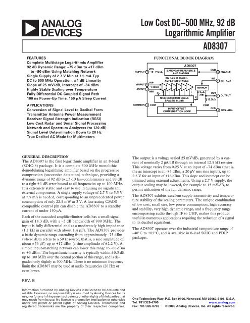
FUNCTIONAL BLOCK DIAGRAM<br />
<strong>AD8307</strong><br />
BAND GAP REFERENCE<br />
AND BIASING<br />
SIX 14.3<strong>dB</strong> 900<strong>MHz</strong><br />
AMPLIFIER STAGES<br />
NINE DETECTOR CELLS<br />
SPACED 14.3<strong>dB</strong><br />
INPUT-OFFSET<br />
COMPENSATION LOOP<br />
ENB<br />
INT<br />
MIRROR<br />
2A OUT<br />
/<strong>dB</strong><br />
2<br />
12.5k<br />
COM<br />
OFS<br />
ENABLE<br />
INT. ADJ<br />
OUTPUT<br />
OFS. ADJ.<br />
GENERAL DESCRIPTION<br />
The <strong>AD8307</strong> is the first logarithmic amplifier in an 8-lead<br />
(SOIC-8) package. It is a complete 500 <strong>MHz</strong> monolithic<br />
demodulating logarithmic amplifier based on the progressive<br />
compression (successive detection) technique, providing a<br />
dynamic range of <strong>92</strong> <strong>dB</strong> to ±3 <strong>dB</strong> law-conformance and 88 <strong>dB</strong><br />
to a tight ±1 <strong>dB</strong> error bound at all frequencies up to 100 <strong>MHz</strong>.<br />
It is extremely stable and easy to use, requiring no significant<br />
external components. A single-supply voltage of 2.7 V to 5.5 V<br />
at 7.5 mA is needed, corresponding to an unprecedented power<br />
consumption of only 22.5 mW at 3 V. A fast-acting CMOS<br />
compatible control pin can disable the <strong>AD8307</strong> to a standby<br />
current of under 150 µA.<br />
Each of the cascaded amplifier/limiter cells has a small-signal<br />
gain of 14.3 <strong>dB</strong>, with a –3 <strong>dB</strong> bandwidth of 900 <strong>MHz</strong>. The<br />
input is fully differential and at a moderately high impedance<br />
(1.1 kΩ in parallel with about 1.4 pF). The <strong>AD8307</strong> provides<br />
a basic dynamic range extending from approximately –75 <strong>dB</strong>m<br />
(where <strong>dB</strong>m refers to a 50 Ω source, that is, a sine amplitude of<br />
about ±56 µV) up to +17 <strong>dB</strong>m (a sine amplitude of ±2.2 V). A<br />
simple input-matching network can lower this range to –88 <strong>dB</strong>m<br />
to +3 <strong>dB</strong>m. The logarithmic linearity is typically within ± 0.3 <strong>dB</strong><br />
up to 100 <strong>MHz</strong> over the central portion of this range, and is degraded<br />
only slightly at 500 <strong>MHz</strong>. There is no minimum frequency<br />
limit; the <strong>AD8307</strong> may be used at audio frequencies (20 Hz) or<br />
even lower.<br />
The output is a voltage scaled 25 mV/<strong>dB</strong>, generated by a current<br />
of nominally 2 µA/<strong>dB</strong> through an internal 12.5 kΩ resistor.<br />
This voltage varies from 0.25 V at an input of –74 <strong>dB</strong>m (that is,<br />
the ac intercept is at –84 <strong>dB</strong>m, a 20 µV rms sine input), up to<br />
2.5 V for an input of +16 <strong>dB</strong>m. This slope and intercept can be<br />
trimmed using external adjustments. Using a 2.7 V supply, the<br />
output scaling may be lowered, for example to 15 mV/<strong>dB</strong>, to<br />
permit utilization of the full dynamic range.<br />
The <strong>AD8307</strong> exhibits excellent supply insensitivity and temperature<br />
stability of the scaling parameters. The unique combination<br />
of low cost, small size, low power consumption, high accuracy<br />
and stability, very high dynamic range, and a frequency range<br />
encompassing audio through IF to UHF, makes this product<br />
useful in numerous applications requiring the reduction of a signal<br />
to its decibel equivalent.<br />
The <strong>AD8307</strong> operates over the industrial temperature range of<br />
–40°C to +85°C, and is available in 8-lead SOIC and PDIP<br />
packages.<br />
REV. B<br />
Information furnished by Analog Devices is believed to be accurate and<br />
reliable. However, no responsibility is assumed by Analog Devices for its<br />
use, nor for any infringements of patents or other rights of third parties that<br />
may result from its use. No license is granted by implication or otherwise<br />
under any patent or patent rights of Analog Devices. Trademarks and<br />
registered trademarks are the property of their respective companies.<br />
One Technology Way, P.O. Box 9106, Norwood, MA 02062-9106, U.S.A.<br />
Tel: 781/329-4700<br />
www.analog.com<br />
Fax: 781/326-8703 © 2003 Analog Devices, Inc. All rights reserved.
<strong>AD8307</strong>–SPECIFICATIONS (V S = 5 V, T A = 25C, R L ≥ 1 M, unless otherwise noted.)<br />
Parameter Conditions Min Typ Max Unit<br />
GENERAL CHARACTERISTICS<br />
Input Range (±1 <strong>dB</strong> Error) Expressed in <strong>dB</strong>m re 50 Ω –72 +16 <strong>dB</strong>m<br />
<strong>Logarithmic</strong> Conformance f ≤ 100 <strong>MHz</strong>, Central 80 <strong>dB</strong> ±0.3 ± 1 <strong>dB</strong><br />
f = 500 <strong>MHz</strong>, Central 75 <strong>dB</strong> ±0.5 <strong>dB</strong><br />
<strong>Logarithmic</strong> Slope Unadjusted 1 23 25 27 mV/<strong>dB</strong><br />
vs. Temperature 23 27 mV/<strong>dB</strong><br />
<strong>Logarithmic</strong> Intercept Sine Amplitude; Unadjusted 2 20 µV<br />
Equivalent Sine Power in 50 Ω –87 –84 –77 <strong>dB</strong>m<br />
vs. Temperature –88 –76 <strong>dB</strong>m<br />
Input Noise Spectral Density Inputs Shorted 1.5 nV/√Hz<br />
Operating Noise Floor R SOURCE = 50 Ω/2 –78 <strong>dB</strong>m<br />
Output Resistance Pin 4 to Ground 10 12.5 15 kΩ<br />
Internal Load Capacitance 3.5 pF<br />
Response Time Small Signal, 10%–90%, 400 ns<br />
0 mV–100 mV, C L = 2 pF<br />
Large Signal, 10%–90%, 500 ns<br />
0 V–2.4 V, C L = 2 pF<br />
Upper Usable Frequency 3 500 <strong>MHz</strong><br />
<strong>Low</strong>er Usable Frequency Input AC-Coupled 10 Hz<br />
AMPLIFIER CELL CHARACTERISTICS<br />
Cell Bandwidth –3 <strong>dB</strong> 900 <strong>MHz</strong><br />
Cell Gain 14.3 <strong>dB</strong><br />
INPUT CHARACTERISTICS<br />
DC Common-Mode Voltage Inputs AC-Coupled 3.2 V<br />
Common-Mode Range Either Input (Small Signal) –0.3 1.6 V S – 1 V<br />
DC Input Offset Voltage 4 R SOURCE ≤ 50 Ω 50 500 µV<br />
Drift 0.8 µV/°C<br />
Incremental Input Resistance Differential 1.1 kΩ<br />
Input Capacitance Either Pin to Ground 1.4 pF<br />
Bias Current Either Input 10 25 µA<br />
POWER INTERFACES<br />
Supply Voltage 2.7 5.5 V<br />
Supply Current V ENB ≥ 2 V 8 10 mA<br />
Disabled V ENB ≤ 1 V 150 750 µA<br />
NOTES<br />
1 This may be adjusted downward by adding a shunt resistor from the output to ground. A 50 k Ω resistor will reduce the nominal slope to 20 mV/<strong>dB</strong>.<br />
2 This may be adjusted in either direction by a voltage applied to Pin 5, with a scale factor of 8 <strong>dB</strong>/V.<br />
3 See the Operation above 500 <strong>MHz</strong> section.<br />
4 Normally nulled automatically by internal offset correction loop. May be manually nulled by a voltage applied between Pin 3 and ground; see the Applications section.<br />
Specifications subject to change without notice.<br />
–2–<br />
REV. B
<strong>AD8307</strong><br />
ABSOLUTE MAXIMUM RATINGS*<br />
Supply Voltage . . . . . . . . . . . . . . . . . . . . . . . . . . . . . . . . . 7.5 V<br />
Input Voltage (Pins 1, 8) . . . . . . . . . . . . . . . . . . . . . . . V SUPPLY<br />
Storage Temperature Range, N, R . . . . . . . . –65°C to +125°C<br />
Ambient Temperature Range, Rated Performance Industrial,<br />
<strong>AD8307</strong>AN, <strong>AD8307</strong>AR . . . . . . . . . . . . . –40°C to +85°C<br />
Lead Temperature Range (Soldering 10 sec) . . . . . . . . . 300°C<br />
*Stresses above those listed under Absolute Maximum Ratings may cause permanent<br />
damage to the device. This is a stress rating only; functional operation of the<br />
device at these or any other conditions above those indicated in the operational<br />
section of this specification is not implied. Exposure to absolute maximum rating<br />
conditions for extended periods may affect device reliability.<br />
ORDERING GUIDE<br />
Model Temperature Range Package Description Package Option<br />
<strong>AD8307</strong>AN –40°C to +85°C 8-Lead Plastic DIP N-8<br />
<strong>AD8307</strong>AR –40°C to +85°C 8-Lead SOIC R-8<br />
<strong>AD8307</strong>AR-REEL –40°C to +85°C 13" REEL R-8<br />
<strong>AD8307</strong>AR-REEL7 –40°C to +85°C 7" REEL R-8<br />
CAUTION<br />
ESD (electrostatic discharge) sensitive device. Electrostatic charges as high as 4000 V readily<br />
accumulate on the human body and test equipment and can discharge without detection. Although the<br />
<strong>AD8307</strong> features proprietary ESD protection circuitry, permanent damage may occur on devices<br />
subjected to high energy electrostatic discharges. Therefore, proper ESD precautions are recommended<br />
to avoid performance degradation or loss of functionality.<br />
PIN CONFIGURATION<br />
PIN FUNCTION DESCRIPTIONS<br />
Pin Name Function<br />
INM<br />
COM<br />
OFS<br />
OUT<br />
1<br />
2<br />
3<br />
4<br />
<strong>AD8307</strong><br />
TOP VIEW<br />
(Not to Scale)<br />
8<br />
7<br />
6<br />
5<br />
INP<br />
VPS<br />
ENB<br />
INT<br />
1 INM Signal Input, Minus Polarity; Normally at V POS /2.<br />
2 COM Common Pin (Usually Grounded).<br />
3 OFS Offset Adjustment; External Capacitor Connection.<br />
4 OUT <strong>Logarithmic</strong> (RSSI) Output Voltage; R OUT = 12.5 kΩ.<br />
5 INT Intercept Adjustment; ±6 <strong>dB</strong> (See Text).<br />
6 ENB CMOS Compatible Chip Enable; Active when High.<br />
7 VPS Positive Supply: 2.7 V to 5.5 V.<br />
8 INP Signal Input, Plus Polarity; Normally at V POS /2.<br />
Due to the symmetrical nature of the response,<br />
there is no special significance to the sign of the<br />
two input pins. DC resistance from INP to INM =<br />
1.1 kΩ.<br />
REV. B<br />
–3–
<strong>AD8307</strong>–Typical Performance Characteristics<br />
8<br />
3<br />
SUPPLY CURRENT (mA)<br />
7<br />
6<br />
5<br />
4<br />
3<br />
2<br />
1<br />
ERROR (<strong>dB</strong>)<br />
2<br />
1<br />
0<br />
–1<br />
–2<br />
TEMPERATURE ERROR @ +85C<br />
TEMPERATURE ERROR @ +25C<br />
TEMPERATURE ERROR @ –40C<br />
0<br />
1.0 1.1 1.2 1.3 1.4 1.5 1.6 1.7 1.8 1.9 2.0<br />
V ENB (V)<br />
TPC 1. Supply Current vs. V ENB Voltage (5 V)<br />
–3<br />
–80 –60 –40 –20 0<br />
20<br />
INPUT LEVEL (<strong>dB</strong>m)<br />
TPC 4. Log Conformance vs. Input Level (<strong>dB</strong>m) at<br />
+25ºC, +85ºC, –40ºC<br />
8<br />
7<br />
3<br />
INPUT FREQUENCY 10<strong>MHz</strong><br />
SUPPLY CURRENT (mA)<br />
6<br />
5<br />
4<br />
3<br />
2<br />
V OUT (V)<br />
2<br />
1<br />
INPUT FREQUENCY 100<strong>MHz</strong><br />
INPUT FREQUENCY 300<strong>MHz</strong><br />
1<br />
INPUT FREQUENCY 500<strong>MHz</strong><br />
0<br />
1.0<br />
1.1 1.2 1.3 1.4 1.5 1.6 1.7<br />
V ENB (V)<br />
1.8 1.9 2.0<br />
0<br />
–80 –60 –40 –20 0<br />
20<br />
INPUT LEVEL (<strong>dB</strong>m)<br />
TPC 2. Supply Current vs. V ENB Voltage (3 V)<br />
TPC 5. V OUT vs. Input Level (<strong>dB</strong>m) at Various Frequencies<br />
3<br />
1.5<br />
2<br />
1.0<br />
ERROR (<strong>dB</strong>)<br />
1<br />
0<br />
–1<br />
FREQUENCY INPUT = 300<strong>MHz</strong><br />
ERROR (<strong>dB</strong>)<br />
0.5<br />
0<br />
–0.5<br />
CFO VALUE = 0.01F<br />
CFO VALUE = 1F<br />
FREQUENCY INPUT = 100<strong>MHz</strong><br />
CFO VALUE = 0.1F<br />
–2<br />
–1.0<br />
–3<br />
–80 –60 –40 –20 0<br />
20<br />
INPUT LEVEL (<strong>dB</strong>m)<br />
TPC 3. Log Conformance vs. Input Level (<strong>dB</strong>m) @<br />
100 <strong>MHz</strong>, 300 <strong>MHz</strong><br />
–1.5<br />
–80 –60 –40 –20 0<br />
20<br />
INPUT LEVEL (<strong>dB</strong>m)<br />
TPC 6. Log Conformance vs. CFO Values at 1 kHz<br />
Input Frequency<br />
–4–<br />
REV. B
<strong>AD8307</strong><br />
3.0<br />
3<br />
V OUT (V)<br />
2.5<br />
2.0<br />
1.5<br />
1.0<br />
INT P IN = 4.0V<br />
10<strong>MHz</strong>, INT = –87.71<strong>dB</strong>m<br />
INT P IN = 3.0V<br />
10<strong>MHz</strong>, INT = –96.52<strong>dB</strong>m<br />
NO CONNECT ON INT<br />
10<strong>MHz</strong>, INT = –82.90<strong>dB</strong>m<br />
ERROR (<strong>dB</strong>)<br />
2<br />
1<br />
0<br />
–1<br />
+INPUT<br />
–INPUT<br />
100<strong>MHz</strong><br />
0.5<br />
–2<br />
0<br />
–80 –70 –60 –50 –40 –30 –20 –10 0 10 20<br />
INPUT LEVEL (<strong>dB</strong>m)<br />
TPC 7. V OUT vs. Input Level at 5 V Supply;<br />
Showing Intercept Adjustment<br />
–3<br />
–80 –60 –40 –20 0<br />
20<br />
INPUT LEVEL (<strong>dB</strong>m)<br />
TPC 10. Log Conformance vs. Input Level at 100 <strong>MHz</strong>;<br />
Showing Response to Alternative Inputs<br />
3.0<br />
3<br />
2.5<br />
INT VOLTAGE<br />
INT = 1.0V, INT = –86<strong>dB</strong>m<br />
2<br />
500<strong>MHz</strong><br />
V OUT (V)<br />
2.0<br />
1.5<br />
INT VOLTAGE<br />
INT NO CONNECT, INT = –71<strong>dB</strong>m<br />
ERROR (<strong>dB</strong>)<br />
1<br />
0<br />
1.0<br />
–1<br />
100<strong>MHz</strong><br />
0.5<br />
INT VOLTAGE<br />
INT = 2.0V, INT = –78<strong>dB</strong>m<br />
–2<br />
0<br />
–80 –70 –60 –50 –40 –30 –20 –10<br />
INPUT LEVEL (<strong>dB</strong>m)<br />
0 10<br />
TPC 8. V OUT vs. Input Level at 3 V Supply Using<br />
AD820 as Buffer, Gain = +2; Showing Intercept<br />
Adjustment<br />
–3<br />
–90 –70 –50 –30 –10 10<br />
INPUT LEVEL (<strong>dB</strong>m)<br />
TPC 11. Log Conformance vs. Input at 100 <strong>MHz</strong>, 500 <strong>MHz</strong>;<br />
Input Driven Differentially Using Transformer<br />
2.5<br />
3<br />
2.0<br />
2<br />
500<strong>MHz</strong><br />
V OUT (V)<br />
1.5<br />
1.0<br />
100<strong>MHz</strong> @ –40C<br />
100<strong>MHz</strong> @ +25C<br />
ERROR (<strong>dB</strong>)<br />
1<br />
0<br />
–1<br />
100<strong>MHz</strong><br />
10<strong>MHz</strong><br />
0.5<br />
100<strong>MHz</strong> @ +85C<br />
–2<br />
0<br />
–80 –60 –40 –20 0<br />
20<br />
INPUT LEVEL (<strong>dB</strong>m)<br />
TPC 9. V OUT vs. Input Level at Three Temperatures<br />
(–40ºC, +25ºC, +85ºC)<br />
–3<br />
–70 –60 –50 –40 –30 –20 –10 0 10<br />
INPUT LEVEL (<strong>dB</strong>m)<br />
TPC 12. Log Conformance vs. Input Level at 3 V<br />
Supply Using AD820 as Buffer, Gain = +2<br />
20<br />
REV. B<br />
–5–
<strong>AD8307</strong><br />
Ch1 200mV<br />
V OUT<br />
CH 1<br />
2V<br />
Ch1 500mV<br />
V OUT<br />
CH 1<br />
V ENB<br />
CH 2<br />
CH 1 GND<br />
INPUT SIGNAL<br />
CH 2<br />
CH 2 GND<br />
GND<br />
Ch2 2.00V<br />
500ns<br />
Ch2 1.00V<br />
200ns<br />
TPC 13. Power-Up Response Time<br />
TPC 16. V OUT Rise Time<br />
V OUT<br />
CH 1<br />
Ch1 200mV<br />
2.5V<br />
Ch1 500mV<br />
V ENB<br />
CH 2<br />
INPUT SIGNAL<br />
CH 2<br />
CH 1 GND<br />
CH 2 GND<br />
V OUT<br />
CH 1<br />
GND<br />
Ch2 2.00V<br />
500ns<br />
Ch2 1.00V<br />
200ns<br />
TPC 14. Power-Down Response Time<br />
TPC 17. Large Signal Response Time<br />
HP8648B<br />
SIGNAL<br />
GENERATOR<br />
RF OUT<br />
52.3<br />
1nF<br />
1nF<br />
VPS = +5.0V<br />
0.1F<br />
INP VPS ENB INT<br />
<strong>AD8307</strong><br />
NC<br />
INM COM OFS OUT<br />
NC<br />
NC = NO CONNECT<br />
HP8112A<br />
PULSE<br />
GENERATOR<br />
TEK P6139A<br />
10x PROBE<br />
OUT<br />
SYNCH OUT<br />
TEK744A<br />
SCOPE<br />
TRIG<br />
HP8648B<br />
SIGNAL<br />
GENERATOR<br />
PULSE<br />
MODULATION<br />
MODE<br />
RF OUT<br />
52.3<br />
10<strong>MHz</strong> REF CLK<br />
PULSE MODE IN<br />
1nF<br />
1nF<br />
VPS = +5.0V<br />
0.1F<br />
INP VPS ENB INT<br />
<strong>AD8307</strong><br />
INM COM OFS OUT<br />
NC = NO CONNECT<br />
NC<br />
EXT TRIG<br />
NC<br />
OUT<br />
TEK P6204<br />
FET PROBE<br />
HP8112A<br />
PULSE<br />
GENERATOR<br />
TEK744A<br />
SCOPE<br />
TRIG<br />
OUT<br />
TRIG<br />
TPC 15. Test Setup for Power-Up/Power-Down<br />
Response Time<br />
TPC 18. Test Setup for V OUT Pulse Response<br />
–6–<br />
REV. B
<strong>AD8307</strong><br />
LOG AMP THEORY<br />
<strong>Logarithmic</strong> amplifiers perform a more complex operation than<br />
that of classical linear amplifiers, and their circuitry is significantly<br />
different. A good grasp of what log amps do, and how they do<br />
it, will avoid many pitfalls in their application. The essential<br />
purpose of a log amp is not to amplify, though amplification is<br />
utilized to achieve the function. Rather, it is to compress a signal<br />
of wide dynamic range to its decibel equivalent. It is thus a<br />
measurement device. A better term might be logarithmic<br />
converter, since its basic function is the conversion of a signal<br />
from one domain of representation to another, via a precise nonlinear<br />
transformation.<br />
<strong>Logarithmic</strong> compression leads to situations that may be confusing<br />
or paradoxical. For example, a voltage offset added to the<br />
output of a log amp is equivalent to a gain increase ahead of its<br />
input. In the usual case where all the variables are voltages, and<br />
regardless of the particular structure, the relationship between the<br />
variables can be expressed as:<br />
V V log V V<br />
(1)<br />
= ( )<br />
OUT Y IN X<br />
where:<br />
V OUT is the output voltage.<br />
V Y is the slope voltage; the logarithm is usually taken to baseten<br />
(in which case V Y is also the volts-per-decade).<br />
V IN is the input voltage.<br />
V X is the intercept voltage.<br />
All log amps implicitly require two references, here, V X and V Y ,<br />
which determine the scaling of the circuit. The absolute accuracy<br />
of a log amp cannot be any better than the accuracy of its<br />
scaling references. Equation 1 is mathematically incomplete in<br />
representing the behavior of a demodulating log amp such as<br />
the <strong>AD8307</strong>, where V IN has an alternating sign. However, the<br />
basic principles are unaffected, and we can safely use this as our<br />
starting point in the analyses of log amp scaling that follow.<br />
V OUT<br />
5V Y<br />
4V Y<br />
3V Y<br />
2V Y<br />
V Y<br />
V OUT = 0<br />
V IN = 10 –2 V X<br />
–40<strong>dB</strong>c<br />
–2V Y<br />
LOWER INTERCEPT<br />
V IN = V X<br />
0<strong>dB</strong>c<br />
V SHIFT<br />
V IN = 10 2 V X<br />
+40<strong>dB</strong>c<br />
V IN = 10 4 V X<br />
+80<strong>dB</strong>c<br />
LOG V IN<br />
Figure 1. Ideal Log Amp Function<br />
Figure 1 shows the input/output relationship of an ideal log amp,<br />
conforming to Equation 1. The horizontal scale is logarithmic<br />
and spans a wide dynamic range, shown here as over 120 <strong>dB</strong>, or<br />
six decades. The output passes through zero (the log-intercept)<br />
at the unique value V IN = V X and would ideally become negative<br />
for inputs below the intercept. In the ideal case, the straight line<br />
describing V OUT for all values of V IN would continue indefinitely<br />
in both directions. The dotted line shows that the effect of adding<br />
an offset voltage V SHIFT to the output is to lower the effective<br />
intercept voltage V X . Exactly the same alteration could be achieved<br />
by raising the gain (or signal level) ahead of the log amp by the<br />
factor V SHIFT /V Y . For example, if V Y is 500 mV per decade<br />
(25 mV/<strong>dB</strong>), an offset of +150 mV added to the output will<br />
appear to lower the intercept by two tenths of a decade, or 6 <strong>dB</strong>.<br />
Adding an offset to the output is thus indistinguishable from<br />
applying an input level that is 6 <strong>dB</strong> higher.<br />
The log amp function described by Equation 1 differs from that<br />
of a linear amplifier in that the incremental gain ∂V OUT /∂V IN is a<br />
very strong function of the instantaneous value of V IN , as is<br />
apparent by calculating the derivative. For the case where the<br />
logarithmic base is e, we have:<br />
∂V<br />
∂V<br />
OUT<br />
IN<br />
V<br />
=<br />
V<br />
Y<br />
IN<br />
That is, the incremental gain is inversely proportional to the<br />
instantaneous value of the input voltage. This remains true for<br />
any logarithmic base, which is chosen as 10 for all decibelrelated<br />
purposes. It follows that a perfect log amp would be<br />
required to have infinite gain under classical small-signal (zeroamplitude)<br />
conditions. Less ideally, this result indicates that,<br />
whatever means are used to implement a log amp, accurate<br />
response under small-signal conditions (that is, at the lower end<br />
of the dynamic range) demands the provision of a very high<br />
gain-bandwidth product. A further consequence of this high<br />
gain is that, in the absence of an input signal, even very small<br />
amounts of thermal noise at the input of a log amp will cause a<br />
finite output for zero input, resulting in the response line curving<br />
away from the ideal shown in Figure 1 toward a finite baseline,<br />
which can be either above or below the intercept. Note that the<br />
value given for this intercept may be an extrapolated value, in<br />
which case the output may not cross zero, or even reach it, as is<br />
the case for the <strong>AD8307</strong>.<br />
While Equation 1 is fundamentally correct, a simpler formula is<br />
appropriate for specifying the calibration attributes of a log amp<br />
like the <strong>AD8307</strong>, which demodulates a sine wave input:<br />
VOUT = VSLOPE ( PIN<br />
− P0 )<br />
(3)<br />
where:<br />
V OUT is the demodulated and filtered baseband (video or RSSI)<br />
output.<br />
V SLOPE is the logarithmic slope, now expressed in V/<strong>dB</strong><br />
(typically between 15 mV/<strong>dB</strong> and 30 mV/<strong>dB</strong>).<br />
P IN is the input power, expressed in decibels relative to some<br />
reference power level.<br />
P 0 is the logarithmic intercept, expressed in decibels relative to<br />
the same reference level.<br />
The most widely used reference in RF systems is decibels above<br />
1 mW in 50 Ω, written <strong>dB</strong>m. Note that the quantity (P IN – P 0 ) is<br />
just <strong>dB</strong>. The logarithmic function disappears from the formula<br />
because the conversion has already been implicitly performed in<br />
stating the input in decibels. This is strictly a concession to<br />
popular convention; log amps manifestly do not respond to<br />
power (tacitly, power absorbed at the input), but rather to input<br />
voltage. The use of <strong>dB</strong>V (decibels with respect to 1 V rms)<br />
would be more precise, though still incomplete, since waveform<br />
is involved, too. Since most users think about and specify RF<br />
(2)<br />
REV. B<br />
–7–
<strong>AD8307</strong><br />
signals in terms of power—more specifically, in <strong>dB</strong>m re 50 Ω —<br />
we will use this convention in specifying the performance of the<br />
<strong>AD8307</strong>.<br />
Progressive Compression<br />
Most high speed, high dynamic range log amps use a cascade of<br />
nonlinear amplifier cells (Figure 2) to generate the logarithmic<br />
function from a series of contiguous segments, a type of piecewise-linear<br />
technique. This basic topology immediately opens<br />
up the possibility of enormous gain-bandwidth products. For<br />
example, the <strong>AD8307</strong> employs six cells in its main signal path,<br />
each having a small-signal gain of 14.3 <strong>dB</strong> (×5.2) and a –3 <strong>dB</strong><br />
bandwidth of about 900 <strong>MHz</strong>; the overall gain is about 20,000<br />
(86 <strong>dB</strong>) and the overall bandwidth of the chain is some 500 <strong>MHz</strong>,<br />
resulting in the incredible gain-bandwidth product (GBW) of<br />
10,000 GHz, about a million times that of a typical op amp.<br />
This very high GBW is an essential prerequisite to accurate<br />
operation under small-signal conditions and at high frequencies.<br />
Equation 2 reminds us, however, that the incremental gain will<br />
decrease rapidly as V IN increases. The <strong>AD8307</strong> continues to<br />
exhibit an essentially logarithmic response down to inputs as<br />
small as 50 µV at 500 <strong>MHz</strong>.<br />
V X A A A A<br />
STAGE 1 STAGE 2 STAGE N – 1 STAGE N<br />
Figure 2. Cascade of Nonlinear Gain Cells<br />
To develop the theory, we will first consider a scheme slightly<br />
different than that employed in the <strong>AD8307</strong>, but simpler to<br />
explain and mathematically more straightforward to analyze.<br />
This approach is based on a nonlinear amplifier unit, which we<br />
may call an A/1 cell, having the transfer characteristic shown in<br />
Figure 3. The local small-signal gain ∂V OUT /∂V IN is A, maintained<br />
for all inputs up to the knee voltage E K , above which the<br />
incremental gain drops to unity. The function is symmetrical: the<br />
same drop in gain occurs for instantaneous values of V IN less<br />
than –E K . The large-signal gain has a value of A for inputs in<br />
the range –E K ≤ V IN ≤ +E K , but falls asymptotically toward unity<br />
for very large inputs. In logarithmic amplifiers based on this<br />
amplifier function, both the slope voltage and the intercept<br />
voltage must be traceable to the one reference voltage, E K .<br />
Therefore, in this fundamental analysis, the calibration accuracy<br />
of the log amp is dependent solely on this voltage. In practice, it<br />
is possible to separate the basic references used to determine V Y<br />
and V X and in the case of the <strong>AD8307</strong>, V Y is traceable to an<br />
A/1<br />
OUTPUT<br />
AE K<br />
0<br />
E K<br />
SLOPE = 1<br />
SLOPE = A<br />
Figure 3. A/1 <strong>Amplifier</strong> Function<br />
INPUT<br />
V W<br />
on-chip band gap reference, while V X is derived from the thermal<br />
voltage kT/q and is later temperature-corrected.<br />
Let the input of an N-cell cascade be V IN , and the final output<br />
V OUT . For small signals, the overall gain is simply A N . A sixstage<br />
system in which A = 5 (14 <strong>dB</strong>) has an overall gain of<br />
15,625 (84 <strong>dB</strong>). The importance of a very high small-signal gain<br />
in implementing the logarithmic function has been noted; however,<br />
this parameter is only of incidental interest in the design of<br />
log amps.<br />
From here onward, rather than considering gain, we will analyze<br />
the overall nonlinear behavior of the cascade in response to a<br />
simple dc input, corresponding to the V IN of Equation 1. For<br />
very small inputs, the output from the first cell is V 1 = AV IN ;<br />
from the second, V 2 = A 2 V IN , and so on, up to V N = A N V IN . At<br />
a certain value of V IN , the input to the Nth cell, V N–1 , is exactly<br />
equal to the knee voltage E K . Thus, V OUT = AE K and since there<br />
are N–1 cells of gain A ahead of this node, we can calculate that<br />
V IN = E K /A N–1 . This unique situation corresponds to the lin-log<br />
transition, labeled ➀ on Figure 4. Below this input, the cascade<br />
of gain cells is acting as a simple linear amplifier, while for higher<br />
values of V IN , it enters into a series of segments that lie on a<br />
logarithmic approximation (dotted line).<br />
V OUT<br />
(4A–3) E K<br />
(3A–2) E K<br />
(2A–1) E K<br />
AE K<br />
0<br />
(A–1) E K<br />
RATIO<br />
OF A<br />
E K /A N–1 E K /A N–2 E K /A N–3 E K /A N–4<br />
Figure 4. First Three Transitions<br />
LOG V IN<br />
Continuing this analysis, we find that the next transition occurs<br />
when the input to the (N–1) stage just reaches E K ; that is, when<br />
V IN = E K /A N–2 . The output of this stage is then exactly AE K ,<br />
and it is easily demonstrated (from the function shown in Figure<br />
3) that the output of the final stage is (2A–1) E K (labeled ➁ on<br />
Figure 4). Thus, the output has changed by an amount (A–1)E K<br />
for a change in V IN from E K /A N–1 to E K /A N–2 , that is, a ratio<br />
change of A. At the next critical point, labeled ➂, we find the input<br />
is again A times larger and V OUT has increased to (3A–2)E K , that<br />
is, by another linear increment of (A–1)E K . Further analysis<br />
shows that right up to the point where the input to the first cell<br />
is above the knee voltage, V OUT changes by (A–1)E K for a ratio<br />
change of A in V IN . This can be expressed as a certain fraction<br />
of a decade, which is simply log 10 (A). For example when A = 5,<br />
a transition in the piecewise linear output function occurs at regular<br />
intervals of 0.7 decade (log 10 (A), or 14 <strong>dB</strong> divided by 20 <strong>dB</strong>).<br />
This insight allows us to immediately write the volts per decade<br />
scaling parameter, which is also the scaling voltage, V Y , when<br />
using base-10 logarithms, as<br />
V<br />
Y<br />
Linear Change in VOUT<br />
= =<br />
Decades Change in V<br />
IN<br />
( A−<br />
1)<br />
E<br />
log 10 A<br />
K<br />
( )<br />
(4)<br />
–8–<br />
REV. B
Note that only two design parameters are involved in determining<br />
V Y , namely, the cell gain A and the knee voltage E K , while N,<br />
the number of stages, is unimportant in setting the slope of the<br />
overall function. For A = 5 and E K = 100 mV, the slope would<br />
be a rather awkward 572.3 mV per decade (28.6 mV/<strong>dB</strong>). A<br />
well designed log amp will have rational scaling parameters.<br />
The intercept voltage can be determined by using two pairs of<br />
transition points on the output function (consider Figure 4).<br />
The result is<br />
V<br />
X<br />
REV. B<br />
EK<br />
=<br />
( N+ 1 ( A−1 ))<br />
(5)<br />
A<br />
For the case under consideration, using N = 6, we calculate<br />
V Z = 4.28 µV. However, we need to be careful about the interpretation<br />
of this parameter, since it was earlier defined as the<br />
input voltage at which the output passes through zero (see Figure<br />
1). But clearly, in the absence of noise and offsets, the output<br />
of the amplifier chain shown in Figure 3 can be zero when,<br />
and only when, V IN = 0. This anomaly is due to the finite gain of<br />
the cascaded amplifier, which results in a failure to maintain the<br />
logarithmic approximation below the lin-log transition (point ➀ in<br />
Figure 4). Closer analysis shows that the voltage given by Equation<br />
5 represents the extrapolated, rather than actual, intercept.<br />
Demodulating Log Amps<br />
Log amps based on a cascade of A/1 cells are useful in baseband<br />
applications because they do not demodulate their input signal.<br />
However, baseband and demodulating log amps alike can be<br />
made using a different type of amplifier stage, which we will call<br />
an A/0 cell. Its function differs from that of the A/1 cell in that<br />
the gain above the knee voltage E K falls to zero, as shown by the<br />
solid line in Figure 5. This is also known as the limiter function,<br />
and a chain of N such cells is often used to generate a hardlimited<br />
output in recovering the signal in FM and PM modes.<br />
A/0<br />
OUTPUT<br />
AE K<br />
0<br />
E K<br />
SLOPE = 0<br />
tanh<br />
SLOPE = A<br />
INPUT<br />
Figure 5. A/0 <strong>Amplifier</strong> Functions (Ideal and tanh)<br />
The AD640, AD606, AD608, <strong>AD8307</strong>, and various other Analog<br />
Devices communications products incorporating a logarithmic<br />
IF amplifier all use this technique. It will be apparent that<br />
the output of the last stage can no longer provide the logarithmic<br />
output, since this remains unchanged for all inputs above<br />
the limiting threshold, which occurs at V IN = E K /A N–1 . Instead,<br />
the logarithmic output is now generated by summing the outputs<br />
of all the stages. The full analysis for this type of log amp is<br />
only slightly more complicated than that of the previous case. It<br />
is readily shown that, for practical purposes, the intercept voltage<br />
V X is identical to that given in Equation 5, while the<br />
slope voltage is<br />
V<br />
Y<br />
AEK<br />
=<br />
(6)<br />
log 10 A<br />
( )<br />
–9–<br />
<strong>AD8307</strong><br />
Preference for the A/0 style of log amp, over one using A/1 cells,<br />
stems from several considerations. The first is that an A/0 cell can<br />
be very simple. In the <strong>AD8307</strong> it is based on a bipolar-transistor<br />
differential pair, having resistive loads R L and an emitter current<br />
source, I E . This will exhibit an equivalent knee voltage of E K =<br />
2kT/q and a small signal gain of A = I E R L /E K . The large signal<br />
transfer function is the hyperbolic tangent (see dotted line in<br />
Figure 5). This function is very precise, and the deviation from<br />
an ideal A/0 form is not detrimental. In fact, the rounded shoulders<br />
of the tanh function result in a lower ripple in the logarithmic<br />
conformance than that obtained using an ideal A/0 function.<br />
An amplifier built of these cells is entirely differential in structure<br />
and can thus be rendered very insensitive to disturbances<br />
on the supply lines and, with careful design, to temperature<br />
variations. The output of each gain cell has an associated<br />
transconductance (g m ) cell, which converts the differential output<br />
voltage of the cell to a pair of differential currents, which are<br />
summed simply by connecting the outputs of all the g m (detector)<br />
stages in parallel. The total current is then converted back<br />
to a voltage by a transresistance stage to generate the logarithmic<br />
output. This scheme is depicted, in single-sided form, in<br />
Figure 6.<br />
A 3 V IN<br />
A 4 V IN<br />
V IN A/0<br />
A/0<br />
A/0<br />
A/0<br />
V LIM<br />
g m<br />
AV IN<br />
g m<br />
A 2 V IN<br />
g m<br />
Figure 6. Log Amp Using A/0 Stages and Auxiliary<br />
Summing Cells<br />
The chief advantage of this approach is that the slope voltage<br />
may now be decoupled from the knee voltage E K = 2 kT/q,<br />
which is inherently PTAT. By contrast, the simple summation<br />
of the cell outputs would result in a very high temperature coefficient<br />
of the slope voltage given by Equation 6. To do this, the<br />
detector stages are biased with currents (not shown in the figure)<br />
which are rendered stable with temperature. These are derived<br />
either from the supply voltage (as in the AD606 and AD608) or<br />
from an internal band gap reference (as in the AD640 and <strong>AD8307</strong>).<br />
This topology affords complete control over the magnitude and<br />
temperature behavior of the logarithmic slope, decoupling it<br />
completely from E K .<br />
A further step is needed to achieve the demodulation response,<br />
required when the log amp is to convert an alternating input<br />
into a quasi-dc baseband output. This is achieved by altering<br />
the g m cells used for summation purposes to also implement the<br />
rectification function. Early discrete log amps based on the<br />
progressive compression technique used half-wave rectifiers.<br />
This made post-detection filtering difficult. The AD640 was the<br />
first commercial monolithic log amp to use a full-wave rectifier,<br />
a practice followed in all subsequent Analog Devices types.<br />
g m<br />
g m<br />
I OUT
<strong>AD8307</strong><br />
We can model these detectors as being essentially linear g m cells,<br />
but producing an output current independent of the sign of the<br />
voltage applied to the input of each cell. That is, they implement<br />
the absolute-value function. Since the output from the later A/0<br />
stages closely approximates an amplitude-symmetric square<br />
wave for even moderate input levels (most stages of the amplifier<br />
chain operate in a limiting mode), the current output from each<br />
detector is almost constant over each period of the input. Somewhat<br />
earlier detector stages produce a waveform having only very<br />
brief dropouts, while the detectors nearest the input produce a low<br />
level, almost-sinusoidal waveform at twice the input frequency.<br />
These aspects of the detector system result in a signal that is easily<br />
filtered, resulting in low residual ripple on the output.<br />
Intercept Calibration<br />
All monolithic log amps from Analog Devices include accurate<br />
means to position the intercept voltage V X (or equivalent power<br />
for a demodulating log amp). Using the scheme shown in<br />
Figure 6, the basic value of the intercept level departs considerably<br />
from that predicted by the simpler analyses given earlier.<br />
However, the intrinsic intercept voltage is still proportional to E K ,<br />
which is PTAT (Equation 5). Recalling that the addition of an<br />
offset to the output produces an effect that is indistinguishable<br />
from a change in the position of the intercept, we can cancel the<br />
left-right motion of V X resulting from the temperature variation of<br />
E K by adding an offset having the required temperature behavior.<br />
The precise temperature-shaping of the intercept-positioning<br />
offset results in a log amp having stable scaling parameters,<br />
making it a true measurement device, for example, as a calibrated<br />
received signal strength indicator (RSSI). In this application,<br />
one is more interested in the value of the output for an<br />
input waveform that is invariably sinusoidal. The input level<br />
may alternatively be stated as an equivalent power, in <strong>dB</strong>m, but<br />
here we must step carefully. It is essential to know the load<br />
impedance in which this power is presumed to be measured.<br />
In RF practice, it is generally safe to assume a reference impedance<br />
of 50 Ω, in which 0 <strong>dB</strong>m (1 mW) corresponds to a sinusoidal<br />
amplitude of 316.2 mV (223.6 mV rms). The intercept may<br />
likewise be specified in <strong>dB</strong>m. For the <strong>AD8307</strong>, it is positioned<br />
at –84 <strong>dB</strong>m, corresponding to a sine amplitude of 20 µV. It is<br />
important to bear in mind that log amps do not respond to<br />
power, but to the voltage applied to their input.<br />
The <strong>AD8307</strong> presents a nominal input impedance much higher<br />
than 50 Ω (typically 1.1 kΩ at low frequencies). A simple input<br />
matching network can considerably improve the sensitivity of<br />
this type of log amp. This will increase the voltage applied to the<br />
input and thus alter the intercept. For a 50 Ω match, the voltage<br />
gain is 4.8 and the whole dynamic range moves down by 13.6 <strong>dB</strong><br />
(see Figure 15). Note that the effective intercept is a function of<br />
waveform. For example, a square wave input will read 6 <strong>dB</strong><br />
higher than a sine wave of the same amplitude and a Gaussian<br />
noise input 0.5 <strong>dB</strong> higher than a sine wave of the same rms value.<br />
Offset Control<br />
In a monolithic log amp, direct coupling between the stages is<br />
used for several reasons. First, this avoids the use of coupling<br />
capacitors, which typically have a chip area equal to that of a<br />
basic gain cell, thus considerably increasing die size. Second,<br />
the capacitor values predetermine the lowest frequency at which<br />
the log amp can operate; for moderate values, this may be as<br />
high as 30 <strong>MHz</strong>, limiting the application range. Third, the<br />
parasitic (backplate) capacitance lowers the bandwidth of the<br />
cell, further limiting the applications.<br />
But the very high dc gain of a direct-coupled amplifier raises a<br />
practical issue. An offset voltage in the early stages of the chain<br />
is indistinguishable from a real signal. For example, if it were as<br />
high as 400 µV, it would be 18 <strong>dB</strong> larger than the smallest ac<br />
signal (50 µV), potentially reducing the dynamic range by this<br />
amount. This problem is averted by using a global feedback<br />
path from the last stage to the first, which corrects this offset in<br />
a similar fashion to the dc negative feedback applied around an<br />
op amp. The high frequency components of the signal must, of<br />
course, be removed, to prevent a reduction of the HF gain in<br />
the forward path.<br />
In the <strong>AD8307</strong>, this is achieved by an on-chip filter, providing<br />
sufficient suppression of HF feedback to allow operation above<br />
1 <strong>MHz</strong>. To extend the range below this frequency, an external<br />
capacitor may be added. This permits the high-pass corner to be<br />
lowered to audio frequencies using a capacitor of modest value.<br />
Note that this capacitor has no effect on the minimum signal<br />
frequency for input levels above the offset voltage: this extends<br />
down to dc (for a signal applied directly to the input pins). The<br />
offset voltage will vary from part to part; some will exhibit<br />
essentially stable offsets of under 100 µV without the benefit<br />
of an offset adjustment.<br />
Extension of Range<br />
The theoretical dynamic range for the basic log amp shown in<br />
Figure 6 is A N . For A = 5.2 (14.3 <strong>dB</strong>) and N = 6, it is 20,000 or<br />
86 <strong>dB</strong>. The actual lower end of the dynamic range is largely<br />
determined by the thermal noise floor, measured at the input of<br />
the chain of amplifiers. The upper end of the range is extended<br />
upward by the addition of top-end detectors. The input signal is<br />
applied to a tapped attenuator, and progressively smaller signals<br />
are applied to three passive rectifying g m cells whose outputs are<br />
summed with those of the main detectors. With care in design,<br />
the extension to the dynamic range can be seamless over the full<br />
frequency range. For the <strong>AD8307</strong>, it amounts to a further 27 <strong>dB</strong>.<br />
Therefore, the total dynamic range is theoretically 113 <strong>dB</strong>. The<br />
specified range of 90 <strong>dB</strong> (–74 <strong>dB</strong>m to +16 <strong>dB</strong>m) is for high<br />
accuracy and calibrated operation, and includes the low end<br />
degradation due to thermal noise and the top end reduction due<br />
to voltage limitations. The additional stages are not, however,<br />
redundant, but are needed to maintain accurate logarithmic<br />
conformance over the central region of the dynamic range, and<br />
in extending the usable range considerably beyond the specified<br />
range. In applications where log conformance is less demanding,<br />
the <strong>AD8307</strong> can provide over 95 <strong>dB</strong> of range.<br />
–10–<br />
REV. B
<strong>AD8307</strong><br />
PRODUCT OVERVIEW<br />
The <strong>AD8307</strong> comprises six main amplifier/limiter stages, each<br />
having a gain of 14.3 <strong>dB</strong> and small signal bandwidth of 900 <strong>MHz</strong>;<br />
the overall gain is 86 <strong>dB</strong> with a –3 <strong>dB</strong> bandwidth of 500 <strong>MHz</strong>.<br />
These six cells, and their associated g m styled full-wave detectors,<br />
handle the lower two-thirds of the dynamic range. Three<br />
top-end detectors, placed at 14.3 <strong>dB</strong> taps on a passive attenuator,<br />
handle the upper third of the 90 <strong>dB</strong> range. Biasing for these<br />
cells is provided by two references: one determines their gain;<br />
the other is a band gap circuit that determines the logarithmic<br />
slope and stabilizes it against supply and temperature variations.<br />
The <strong>AD8307</strong> may be enabled/disabled by a CMOS compatible<br />
level at ENB (Pin 6). The first amplifier stage provides a low<br />
voltage noise spectral density (1.5 nV/√Hz).<br />
The differential current-mode outputs of the nine detectors are<br />
summed and then converted to single-sided form in the output<br />
stage, nominally scaled 2 µA/<strong>dB</strong>. The logarithmic output voltage<br />
is developed by applying this current to an on-chip 12.5 kΩ<br />
resistor, resulting in a logarithmic slope of 25 mV/<strong>dB</strong> (i.e.,<br />
500 mV/decade) at OUT. This voltage is not buffered, allowing<br />
the use of a variety of special output interfaces, including the<br />
addition of post-demodulation filtering. The last detector stage<br />
includes a modification to temperature-stabilize the log intercept,<br />
which is accurately positioned to make optimal use of the full<br />
output voltage range available. The intercept may be adjusted<br />
using the INT pin, which adds or subtracts a small current to<br />
the signal current.<br />
junction capacitances associated with them, due to active<br />
devices or ESD protection; these may be neither accurate nor<br />
stable. Component numbering in each of these interface diagrams<br />
is local.<br />
Enable Interface<br />
The chip-enable interface is shown in Figure 8. The currents in<br />
the diode-connected transistors control the turn-on and turn-off<br />
states of the band gap reference and the bias generator, and are a<br />
maximum of 100 µA when Pin 6 is taken to 5 V, under worst-case<br />
conditions. Left unconnected, or at a voltage below 1 V, the<br />
<strong>AD8307</strong> will be disabled and consume a sleep current of under<br />
50 µA; tied to the supply, or a voltage above 2 V, it will be fully<br />
enabled. The internal bias circuitry is very fast (typically
<strong>AD8307</strong><br />
In most applications, the signal will be single-sided and may be<br />
applied to either Pin 1 or Pin 8, with the other pin ac-coupled to<br />
ground. Under these conditions, the largest input signal that can<br />
be handled by the <strong>AD8307</strong> is 10 <strong>dB</strong>m (sine amplitude of ±1 V)<br />
when operating from a 3 V supply; 16 <strong>dB</strong>m may be handled<br />
using a 5 V supply. The full 16 <strong>dB</strong>m may be achieved for supplies<br />
down to 2.7 V, using a fully balanced drive. For frequencies<br />
above about 10 <strong>MHz</strong>, this is most easily achieved using a matching<br />
network (see below). Using such a network, having an inductor<br />
at the input, the input transient noted above is eliminated. Occasionally,<br />
it may be desirable to use the dc-coupled potential of<br />
the <strong>AD8307</strong>. The main challenge here is to present signals to<br />
the log amp at the elevated common-mode input level, requiring<br />
the use of low noise, low offset buffer amplifiers. Using dual<br />
supplies of ±3 V, the input pins may operate at ground potential.<br />
Offset Interface<br />
The input-referred dc offsets in the signal path are nulled via<br />
the interface associated with Pin 3, shown in Figure 10. Q1 and<br />
Q2 are the first stage input transistors, with their corresponding<br />
load resistors (125 Ω). Q3 and Q4 generate small currents,<br />
which can introduce a dc offset into the signal path. When the<br />
voltage on OFS is at about 1.5 V, these currents are equal, and<br />
nominally 16 µA. When OFS is taken to ground, Q4 is off and<br />
the effect of the current in Q3 is to generate an offset voltage of<br />
16 µA × 125 Ω = 2 mV. Since the first stage gain is ×5, this is<br />
equivalent to a input offset (INP to INM) of 400 µV. When<br />
OFS is taken to its most positive value, the input-referred offset<br />
is reversed, to –400 µV. If true dc coupling is needed, down to<br />
very small inputs, this automatic loop must be disabled, and<br />
the residual offset eliminated using a manual adjustment, as<br />
explained in the next section.<br />
In normal operation, however, using an ac-coupled input signal,<br />
the OFS pin should be left open. Any residual input-offset voltage<br />
is then automatically nulled by the action of the feedback<br />
loop. The g m cell, which is gated off when the chip is disabled,<br />
converts any output offset (sensed at a point near the end of the<br />
cascade of amplifiers) to a current. This is integrated by the onchip<br />
capacitor C HP , plus any added external capacitance C OFS ,<br />
so as to generate an error voltage, which is applied back to the<br />
input stage in the polarity needed to null the output offset. From<br />
a small-signal perspective, this feedback alters the response of<br />
the amplifier, which, rather than behaving as a fully dc-coupled<br />
system, now exhibits a zero in its ac transfer function, resulting<br />
in a closed-loop high-pass corner at about 700 kHz.<br />
The offset feedback is limited to a range of ±400 µV; signals<br />
larger than this override the offset control loop, which only impacts<br />
performance for very small inputs. An external capacitor reduces<br />
the high-pass corner to arbitrarily low frequencies; using 1 µF<br />
this corner is below 10 Hz. All ADI log amps use an offsetnulling<br />
loop; the <strong>AD8307</strong> differs in using this single-sided form.<br />
Output Interface<br />
The outputs from the nine detectors are differential currents,<br />
having an average value that is dependent on the signal input level,<br />
plus a fluctuation at twice the input frequency. The currents are<br />
summed at nodes LGP and LGM in Figure 11. Further currents<br />
are added at these nodes, to position the intercept, by slightly<br />
raising the output for zero input, and to provide temperature<br />
compensation. Since the <strong>AD8307</strong> is not laser-trimmed, there<br />
is a small uncertainty in both the log slope and the log intercept.<br />
These scaling parameters may be adjusted (see below).<br />
For zero-signal conditions, all the detector output currents are<br />
equal. For a finite input of either polarity, their difference is<br />
converted by the output interface to a single-sided unipolar<br />
current nominally scaled 2 µA/<strong>dB</strong> (40 µA/decade), at the output<br />
pin OUT. An on-chip 12.5 kΩ resistor, R1, converts this current<br />
to a voltage of 25 mV/<strong>dB</strong>. C1 and C2 are effectively in shunt<br />
with R1 and form a low-pass filter pole with a corner frequency<br />
of about 5 <strong>MHz</strong>. The pulse response settles to within 1% of the<br />
final value within 300 ns. This integral low-pass filter provides<br />
adequate smoothing in many IF applications. At 10.7 <strong>MHz</strong>, the<br />
2f ripple is 12.5 mV in amplitude, equivalent to ±0.5 <strong>dB</strong>, and<br />
only 0.5 mV (±0.02 <strong>dB</strong>) at f = 50 <strong>MHz</strong>. A filter capacitor C FLT<br />
added from OUT to ground will lower this corner frequency.<br />
Using 1 µF, the ripple is maintained to less than ±0.5 <strong>dB</strong> down<br />
to input frequencies of 100 Hz. Note that C OFS (above) should<br />
also be increased in low frequency applications, and will typically<br />
be made equal to C FLT .<br />
It may be desirable to increase the speed of the output response,<br />
with the penalty of increased ripple. One way to do this is simply<br />
by connecting a shunt load resistor from OUT to ground,<br />
which raises the low-pass corner frequency. This also alters the<br />
logarithmic slope, for example to 7.5 mV/<strong>dB</strong> using a 5.36 kΩ<br />
resistor, while reducing the 10% to 90% rise time to 25 ns.<br />
The ripple amplitude for 50 <strong>MHz</strong> input remains 0.5 mV, but<br />
this is now equivalent to ±0.07 <strong>dB</strong>. If a negative supply is available,<br />
the output pin may be connected directly to the summing<br />
node of an external op amp connected as an inverting-mode<br />
transresistance stage.<br />
INPUT<br />
STAGE<br />
BIAS, 1.2V<br />
Q1<br />
125<br />
Q2<br />
16A AT<br />
BALANCE<br />
Q3<br />
36k<br />
Q4<br />
48k<br />
MAIN GAIN<br />
STAGES<br />
OFS<br />
S<br />
g m<br />
AVERAGE<br />
ERROR<br />
CURRENT<br />
VPS<br />
TO LAST<br />
DETECTOR<br />
C OFS C HP<br />
COM<br />
Figure 10. Offset Interface and Offset-Nulling Path<br />
LGP<br />
LGM<br />
25mV/<strong>dB</strong><br />
OUT<br />
C FLT<br />
3pF<br />
FROM ALL<br />
DETECTORS<br />
2A/<strong>dB</strong><br />
0-220A<br />
C1<br />
2.5pF<br />
1.25k<br />
1.25k<br />
C2<br />
1pF<br />
R1<br />
12.5k<br />
1.25k<br />
1.25k<br />
400mV<br />
8.25k<br />
60k<br />
BIAS<br />
60A<br />
Figure 11. Simplified Output Interface<br />
VPS<br />
INT<br />
COM<br />
–12–<br />
REV. B
<strong>AD8307</strong><br />
USING THE <strong>AD8307</strong><br />
The <strong>AD8307</strong> has very high gain and a bandwidth from dc to<br />
over 1 GHz, at which frequency the gain of the main path is still<br />
over 60 <strong>dB</strong>. Consequently, it is susceptible to all signals within<br />
this very broad frequency range that find their way to the input<br />
terminals. It is important to remember that these are quite indistinguishable<br />
from the wanted signal, and will have the effect of<br />
raising the apparent noise floor (that is, lowering the useful<br />
dynamic range). For example, while the signal of interest may<br />
be an IF of 50 <strong>MHz</strong>, any of the following could easily be larger<br />
than the IF signal at the lower extremities of its dynamic range:<br />
60 Hz hum, picked up due to poor grounding techniques; spurious<br />
coupling from a digital clock source on the same PC board; local<br />
radio stations; and so on.<br />
Careful shielding is essential. A ground plane should be used to<br />
provide a low impedance connection to the common pin COM,<br />
for the decoupling capacitor(s) used at VPS, and as the output<br />
ground. It is inadvisable to assume that the ground plane is an<br />
equipotential. Neither of the inputs should be ac-coupled<br />
directly to the ground plane, but should be kept separate from<br />
it, being returned instead to the low associated with the source.<br />
This may mean isolating the low side of an input connector with<br />
a small resistance to the ground plane.<br />
Basic Connections<br />
Figure 12 shows the simple connections suitable for many applications.<br />
The inputs are ac-coupled by C1 and C2, which should<br />
have the same value, say, C C . The coupling time constant is<br />
R IN C C /2, thus forming a high-pass corner with a 3 <strong>dB</strong> attenuation<br />
at f HP = 1/(pR IN C C ). In high frequency applications, f HP should<br />
be as large as possible in order to minimize the coupling of<br />
unwanted low frequency signals. Conversely, in low frequency<br />
applications, a simple RC network forming a low-pass filter<br />
should be added at the input for the same reason. For the case<br />
where the generator is not terminated, the signal range should<br />
be expressed in terms of the voltage response, and extends from<br />
–85 <strong>dB</strong>V to +6 <strong>dB</strong>V.<br />
INPUT<br />
–75<strong>dB</strong>m TO<br />
+16<strong>dB</strong>m<br />
4.7<br />
C1 = C C<br />
NC<br />
R<br />
INP VPS ENB INT<br />
IN <br />
R T <strong>AD8307</strong><br />
1.1k<br />
INM COM OFS OUT<br />
C2 = C C<br />
0.1F<br />
NC<br />
NC = NO CONNECT<br />
V P , 2.7V–5.5V<br />
AT 8mA<br />
OUTPUT<br />
25mV/<strong>dB</strong><br />
Figure 12. Basic Connections<br />
Where it is necessary to terminate the source at a low impedance,<br />
the resistor R T should be added, with allowance for the<br />
shunting effect of the basic 1.1 kΩ input resistance (R IN ) of the<br />
<strong>AD8307</strong>. For example, to terminate a 50 Ω source, a 52.3 Ω 1%<br />
tolerance resistor should be used. This may be placed on the<br />
input side or the log-amp side of the coupling capacitors; in<br />
the former case, smaller capacitors can be used for a given<br />
frequency range; in the latter case, the effective R IN is lowered<br />
directly at the log-amp inputs.<br />
Figure 13 shows the output versus the input level, in <strong>dB</strong>m, when<br />
driven from a terminated 50 Ω generator, for sine inputs at<br />
10 <strong>MHz</strong>, 100 <strong>MHz</strong>, and 500 <strong>MHz</strong>; Figure 14 shows the typical<br />
logarithmic conformance under the same conditions. Note that<br />
+10 <strong>dB</strong>m corresponds to a sine amplitude of 1 V, equivalent to<br />
an rms power of 10 mW in a 50 Ω termination. But if the termination<br />
resistor is omitted, the input power is negligible. The use<br />
of <strong>dB</strong>m to define input level therefore needs to be considered<br />
carefully in connection with the <strong>AD8307</strong>.<br />
OUTPUT VOLTAGE (V)<br />
3.0<br />
2.5<br />
2.0<br />
1.5<br />
1.0<br />
0.5<br />
500<strong>MHz</strong><br />
10<strong>MHz</strong><br />
100<strong>MHz</strong><br />
0<br />
–80 –70 –60 –50 –40 –30 –20 –10 0 10 20<br />
INPUT LEVEL (<strong>dB</strong>m)<br />
Figure 13. Log Response at 10 <strong>MHz</strong>, 100 <strong>MHz</strong>, and 500 <strong>MHz</strong><br />
ERROR (<strong>dB</strong>)<br />
5<br />
4<br />
3<br />
2<br />
1<br />
0<br />
–1<br />
–2<br />
–3<br />
–4<br />
10<strong>MHz</strong><br />
500<strong>MHz</strong><br />
100<strong>MHz</strong><br />
–5<br />
–80 –70 –60 –50 –40 –30 –20 –10 0 10 20<br />
INPUT LEVEL (<strong>dB</strong>m)<br />
Figure 14. <strong>Logarithmic</strong> Law Conformance at 10 <strong>MHz</strong>,<br />
100 <strong>MHz</strong>, and 500 <strong>MHz</strong><br />
Input Matching<br />
Where higher sensitivity is required, an input matching network<br />
is valuable. Using a transformer to achieve the impedance transformation<br />
also eliminates the need for coupling capacitors,<br />
lowers the offset voltage generated directly at the input, and<br />
balances the drives to INP and INM. The choice of turns ratio<br />
will depend somewhat on the frequency. At frequencies below<br />
50 <strong>MHz</strong>, the reactance of the input capacitance is much higher<br />
than the real part of the input impedance. In this frequency range,<br />
a turns ratio of about 1:4.8 will lower the input impedance to<br />
50 Ω while raising the input voltage, thus lowering the effect of<br />
the short circuit noise voltage by the same factor. There will be<br />
a small contribution from the input noise current, so the total<br />
noise will be reduced by a somewhat smaller factor. The intercept<br />
will also be lowered by the turns ratio; for a 50 Ω match, it will<br />
be reduced by 20 log 10 (4.8) or 13.6 <strong>dB</strong>.<br />
REV. B<br />
–13–
<strong>AD8307</strong><br />
Narrow-Band Matching<br />
Transformer coupling is useful in broadband applications. However,<br />
a magnetically coupled transformer may not be convenient<br />
in some situations. At high frequencies, it is often preferable to<br />
use a narrow-band matching network, as shown in Figure 15.<br />
This has several advantages. The same voltage gain is achieved,<br />
providing increased sensitivity, but now a measure of selectivity<br />
is also introduced. The component count is low: two capacitors<br />
and an inexpensive chip inductor. Further, by making these<br />
capacitors unequal, the amplitudes at INP and INM may be<br />
equalized when driving from a single-sided source; that is, the<br />
network also serves as a balun. Figure 16 shows the response for<br />
a center frequency of 100 <strong>MHz</strong>; note the very high attenuation<br />
at low frequencies. The high frequency attenuation is due to the<br />
input capacitance of the log amp.<br />
50 INPUT<br />
–88<strong>dB</strong>m TO<br />
+3<strong>dB</strong>m<br />
C1<br />
Z IN = 50<br />
C2<br />
L M<br />
0.1F<br />
INP VPS ENB INT<br />
<strong>AD8307</strong><br />
4.7<br />
NC<br />
INM COM OFS OUT<br />
NC = NO CONNECT<br />
NC<br />
V P , 2.7V–5.5V<br />
AT 8mA<br />
OUTPUT<br />
25mV/<strong>dB</strong><br />
Figure 15. High Frequency Input Matching Network<br />
DECIBELS<br />
14<br />
13<br />
12<br />
11<br />
10<br />
9<br />
8<br />
7<br />
6<br />
5<br />
4<br />
3<br />
2<br />
1<br />
0<br />
GAIN<br />
INPUT<br />
–1<br />
60 70 80 90 100 110 120 130 140 150<br />
FREQUENCY (<strong>MHz</strong>)<br />
Figure 16. Response of 100 <strong>MHz</strong> Matching Network<br />
Table I provides solutions for a variety of center frequencies F C<br />
and matching impedances Z IN of nominally 50 Ω and 100 Ω.<br />
The unequal capacitor values were chosen to provide a well<br />
balanced differential drive, and also to allow better centering of<br />
the frequency response peak when using standard value components;<br />
this generally results in a Z IN that is not exact. The full<br />
<strong>AD8307</strong> HF input impedance and the inductor losses were<br />
included in the modeling.<br />
Table I. Narrow-Band Matching Values<br />
F C Z IN C1 C2 L M Voltage<br />
(<strong>MHz</strong>) (Ω) (pF) (pF) (nH) Gain (<strong>dB</strong>)<br />
10 45 160 150 3300 13.3<br />
20 44 82 75 1600 13.4<br />
50 46 30 27 680 13.4<br />
100 50 15 13 330 13.4<br />
150 57 10 8.2 220 13.2<br />
200 57 7.5 6.8 150 12.8<br />
250 50 6.2 5.6 100 12.3<br />
500 54 3.9 3.3 39 10.9<br />
10 103 100 91 5600 10.4<br />
20 102 51 43 2700 10.4<br />
50 99 22 18 1000 10.6<br />
100 98 11 9.1 430 10.5<br />
150 101 7.5 6.2 260 10.3<br />
200 95 5.6 4.7 180 10.3<br />
250 <strong>92</strong> 4.3 3.9 130 9.9<br />
500 114 2.2 2.0 47 6.8<br />
Slope and Intercept Adjustments<br />
Where higher calibration accuracy is needed, the adjustments<br />
shown in Figure 17 can be used, either singly or in combination.<br />
The log slope is lowered to 20 mV/<strong>dB</strong> by shunting the nominally<br />
12.5 kΩ on-chip load resistor (see Figure 11) with 50 kΩ, adjusted<br />
by VR1. The calibration range is ±10% (18 mV/<strong>dB</strong> to 22 mV/<strong>dB</strong>),<br />
including full allowance for the variability in the value of the<br />
internal load. The adjustment may be made by alternately applying<br />
two input levels, provided by an accurate signal generator, spaced<br />
over the central portion of the log amp’s dynamic range, for<br />
example –60 <strong>dB</strong>m and 0 <strong>dB</strong>m. An AM-modulated signal, at the<br />
center of the dynamic range, can also be used. For a modulation<br />
depth M, expressed as a fraction, the decibel range between the<br />
peaks and troughs over one cycle of the modulation period is<br />
given by<br />
1 + M<br />
∆ <strong>dB</strong> = 20 log 10<br />
(7)<br />
1 − M<br />
For example, using an rms signal level of –40 <strong>dB</strong>m with a 70%<br />
modulation depth (M = 0.7), the decibel range is 15 <strong>dB</strong>, as the<br />
signal varies from –47.5 <strong>dB</strong>m to –32.5 <strong>dB</strong>m.<br />
The log intercept is adjustable over a ±3 <strong>dB</strong> range, which is<br />
sufficient to absorb the worst-case intercept error in the <strong>AD8307</strong><br />
plus some system-level errors. For greater range, set R S to zero.<br />
VR2 is adjusted while applying an accurately known CW signal<br />
near the lower end of the dynamic range in order to minimize<br />
the effect of any residual uncertainty in the slope. For example,<br />
to position the intercept to –80 <strong>dB</strong>m, a test level of –65 <strong>dB</strong>m<br />
may be applied and VR2 adjusted to produce a dc output of<br />
15 <strong>dB</strong> above zero at 25 mV/<strong>dB</strong>, which is +0.3 V.<br />
INPUT<br />
–75<strong>dB</strong>m TO<br />
+16<strong>dB</strong>m<br />
0.1F<br />
4.7<br />
VR2<br />
R S<br />
C1 = C 50k<br />
C<br />
C2 = C C<br />
NC = NO CONNECT<br />
INP VPS ENB INT<br />
<strong>AD8307</strong><br />
INM COM OFS OUT<br />
NC<br />
32.4k<br />
3<strong>dB</strong><br />
V P , 2.7V–5.5V<br />
AT 8mA<br />
FOR V P = 3V, R S = 20k<br />
V P = 5V, R S = 51k<br />
VR1<br />
50k<br />
20mV/<strong>dB</strong><br />
10%<br />
Figure 17. Slope and Intercept Adjustments<br />
–14–<br />
REV. B
<strong>AD8307</strong><br />
APPLICATIONS<br />
The <strong>AD8307</strong> is a highly versatile and easily applied log amp<br />
requiring very few external components. Most applications of<br />
this product can be accommodated using the simple connections<br />
shown in the preceding section. A few examples of more<br />
specialized applications are provided here.<br />
Buffered Output<br />
The output may be buffered, and the slope optionally increased,<br />
using an op amp. If the single-supply capability is to be preserved,<br />
a suitable component is the AD8031. Like the <strong>AD8307</strong>, it is<br />
capable of operating from a 2.7 V supply and features a rail-torail<br />
output capability; it is available in a 5-lead version and in dual<br />
form as the 8-lead AD8032. Figure 18 shows how the slope may<br />
be increased to 50 mV/<strong>dB</strong> (1 V per decade), requiring a 5 V<br />
supply (90 <strong>dB</strong> times 50 mV is a 4.5 V swing). VR1 provides a<br />
±10% slope adjustment; VR2 provides a ±3 <strong>dB</strong> intercept range.<br />
With R2 = 4.99 kΩ, the slope is adjustable to 25 mV/<strong>dB</strong>, allowing<br />
the use of a 2.7 V supply. Setting R2 to 80.6 kΩ, it is raised<br />
to 100 mV/<strong>dB</strong>, providing direct reading in decibels on a digital<br />
voltmeter. Since a 90 <strong>dB</strong> range now corresponds to a 9 V swing,<br />
a supply of at least this amount is needed for the op amp.<br />
INPUT<br />
–75<strong>dB</strong>m TO<br />
+16<strong>dB</strong>m<br />
0.1F<br />
INP VPS ENB INT<br />
<strong>AD8307</strong><br />
INM COM OFS OUT<br />
NC<br />
VR2<br />
50k<br />
32.4k<br />
4.7<br />
3<strong>dB</strong><br />
VR1<br />
50k<br />
R S<br />
AD8031<br />
20mV/<strong>dB</strong><br />
NC = NO CONNECT<br />
C1<br />
V P , 2.7V–5.5V<br />
FOR V P = 3V, R S = 20k<br />
V P = 5V, R S = 51k<br />
R1<br />
20k<br />
OUTPUT<br />
50mV/<strong>dB</strong><br />
10%<br />
R2<br />
30.1k<br />
COM<br />
Figure 18. Log Amp with Buffered Output<br />
C1 is optional; it lowers the corner frequency of the low-pass<br />
output filter. A value of 0.1 µF should be used for applications<br />
in which the output is measured on a voltmeter or other low<br />
speed device. On the other hand, when C1 is omitted, the 10%<br />
to 90% response time is under 200 ns and is typically 300 ns to<br />
99% of final value. To achieve faster response times, it is necessary<br />
to lower the load resistance at the output of the <strong>AD8307</strong>,<br />
then restore the scale using a higher gain in the op amp. Using<br />
8.33 kΩ, the basic slope is 10 mV/<strong>dB</strong>; this can be restored to<br />
25 mV/<strong>dB</strong> using a buffer gain of 2.5. The overall 10% to 90%<br />
response time is under 100 ns. Figure 19 shows how the output<br />
current capability can be augmented to drive a 50 Ω load; R T<br />
optionally provides reverse termination, which halves the slope<br />
to 12.5 mV/<strong>dB</strong>.<br />
Four-Pole Filter<br />
In low frequency applications, for example, audio down to<br />
20 Hz, it is useful to employ the buffer amplifier as a multipole<br />
low-pass filter in order to achieve low output ripple while maintaining<br />
a rapid response time to changes in signal level.<br />
INPUT<br />
–75<strong>dB</strong>m TO<br />
+16<strong>dB</strong>m<br />
0.1F<br />
INP VPS ENB INT<br />
<strong>AD8307</strong><br />
INM COM OFS OUT<br />
NC<br />
VR2<br />
50k<br />
6.34k<br />
4.7<br />
3<strong>dB</strong><br />
R S (SEE FIGURE 36)<br />
10mV/<strong>dB</strong> 18%<br />
VR1<br />
5k<br />
AD8031<br />
NC = NO CONNECT<br />
R1<br />
2k<br />
2N3904<br />
25mV/<strong>dB</strong><br />
R2<br />
3.01k<br />
Figure 19. Cable-Driving Log Amp<br />
V P , 2.7–5.5V<br />
R T<br />
(OPTIONAL)<br />
OUTPUT<br />
50<br />
MIN<br />
COM<br />
In Figure 20, the capacitor values were chosen for operation in<br />
the audio field, providing a corner frequency of 10 Hz, an attenuation<br />
of 80 <strong>dB</strong>/decade above this frequency, and a 1% settling<br />
time of 150 ms (0.1% in 175 ms). The residual ripple is 4 mV<br />
(± 0.02 <strong>dB</strong>) when the input to the <strong>AD8307</strong> is at 20 Hz. This<br />
filter may easily be adapted to other frequencies by proportional<br />
scaling of C5–C7 (e.g., for 100 kHz use 100 pF). Placed ahead<br />
of a digital multimeter, the convenient slope scaling of 100 mV/<strong>dB</strong><br />
requires only a repositioning of the decimal point to read directly in<br />
decibels. The supply voltage for the filter must be large enough<br />
to support the dynamic range; a minimum of 9 V is needed for<br />
most applications; 12 V is recommended.<br />
INPUT<br />
5mV TO<br />
160V rms<br />
C3<br />
2.5nF<br />
R1<br />
50k<br />
C1<br />
10F<br />
0.1F<br />
INP VPS ENB INT<br />
<strong>AD8307</strong><br />
NC<br />
INM COM OFS OUT<br />
C2<br />
10F<br />
4.7<br />
VR1<br />
2k<br />
422<br />
INT 4<strong>dB</strong><br />
C4<br />
1F<br />
V P<br />
C5<br />
1F<br />
34k<br />
VR2<br />
50k<br />
SLOPE C6<br />
32.4k<br />
1F<br />
OP AMP IS AD8032<br />
SCALE C1–C8 AS NEEDED<br />
(SEE TEXT). NOTE POLARITIES<br />
IF TANTALUM CAPACITORS<br />
ARE USED.<br />
7.32k<br />
100k<br />
34k<br />
80.6k<br />
C8<br />
1F<br />
C7<br />
1F<br />
OUTPUT<br />
100mV/<strong>dB</strong><br />
75k<br />
93k<br />
COM<br />
Figure 20. Log Amp with Four-Pole <strong>Low</strong>-Pass Filter<br />
Figure 20 also shows the use of an input attenuator that may<br />
optionally be employed here, or in any other of these applications,<br />
to produce a useful wide-range ac voltmeter with direct-decibel<br />
scaling. The basic range of –73 <strong>dB</strong>m to +17 <strong>dB</strong>m (that is, 50 µV<br />
rms to 1.6 V rms, for sine excitations) is shifted for illustrative<br />
purposes to 5 mV to 160 V rms (at which point the power in R1<br />
is 512 mW). Because the basic input resistance of the <strong>AD8307</strong><br />
is not precise, VR1 is used to center the signal range at its input,<br />
doubling as a ±4 <strong>dB</strong> intercept adjustment. The low frequency<br />
response extends to 15 Hz; a higher corner frequency can be selected<br />
as needed by scaling C1 and C2. The shunt capacitor C3 is<br />
used to lower the high frequency bandwidth to about 100 kHz, and<br />
thus lower the susceptibility to spurious signals. Other values<br />
should be chosen as needed for the coupling and filter capacitors.<br />
REV. B<br />
–15–
<strong>AD8307</strong><br />
1 mW to 1 kW 50 Ω Power Meter<br />
The front-end adaptation shown in Figure 21 provides the<br />
measurement of power being delivered from a transmitter final<br />
amplifier to an antenna. The range has been set to cover the power<br />
range –30 <strong>dB</strong>m (7.07 mV rms, or 1 µW) to +60 <strong>dB</strong>m (223 V rms,<br />
or 1 kW). A nominal voltage attenuation ratio of 158:1 (44 <strong>dB</strong>) is<br />
used; thus the intercept is moved from –84 <strong>dB</strong>m to –40 <strong>dB</strong>m and<br />
the <strong>AD8307</strong>, scaled 0.25 V/decade of power, will now read 1.5 V<br />
for a power level of 100 mW, 2.0 V at 10 W and 2.5 V at 1 kW.<br />
The general expression is<br />
P ( <strong>dB</strong>m)= 40 ( V OUT −1)<br />
The required attenuation could be implemented using a capacitive<br />
divider, providing a very low input capacitance, but it is difficult<br />
to ensure accurate values of small capacitors. A better approach<br />
is to use a resistive divider, taking the required precautions to<br />
minimize spurious coupling into the <strong>AD8307</strong> by placing it in a<br />
shielded box, with the input resistor passing through a hole in this<br />
box, as indicated in the figure. The coupling capacitors shown here<br />
are suitable for f ≥ 10 <strong>MHz</strong>. A capacitor may be added across<br />
the input pins of the <strong>AD8307</strong> to reduce the response to spurious<br />
HF signals, which, as already noted, extends to over 1 GHz.<br />
The mismatch caused by the loading of this resistor will be<br />
trivial; only 0.05% of the power delivered to the load will be<br />
absorbed by the measurement system, a maximum of 500 mW<br />
at 1 kW. The post-demodulation filtering and slope-calibration<br />
arrangements should be chosen from other applications described<br />
here, to meet the particular system requirements. The 1 nF<br />
capacitor lowers the risk of HF signals entering the <strong>AD8307</strong> via<br />
the load.<br />
TO<br />
ANTENNA<br />
50 INPUT<br />
FROM P.A.<br />
1W TO<br />
1kW<br />
100k<br />
1/2W<br />
51pF<br />
VR1<br />
2k<br />
INT 3<strong>dB</strong><br />
604<br />
51pF<br />
NC = NO CONNECT<br />
0.1F<br />
INP VPS ENB INT<br />
<strong>AD8307</strong><br />
NC<br />
INM COM OFS OUT<br />
NC<br />
1nF<br />
22<br />
2k<br />
V P<br />
LEAD-<br />
THROUGH<br />
CAPACITORS,<br />
1nF<br />
OUTPUT<br />
Figure 21. 1 µW to 1 kW 50 Ω Power Meter<br />
+5V<br />
V OUT<br />
Measurement System with 120 <strong>dB</strong> Dynamic Range<br />
The dynamic range of the <strong>AD8307</strong> can be extended further—<br />
from 90 <strong>dB</strong> to over 120 <strong>dB</strong>—by the addition of an X-AMP®<br />
such as the AD603. This type of variable gain amplifier exhibits<br />
a very exact exponential gain control characteristic, which is<br />
another way of stating that the gain varies by a constant number<br />
of decibels for a given change in the control voltage. For the<br />
AD603, this scaling factor is 40 <strong>dB</strong>/V, or 25 mV/<strong>dB</strong>. It will be<br />
apparent that this property of a linear-in-<strong>dB</strong> response is characteristic<br />
of log amps; indeed, the <strong>AD8307</strong> exhibits the same<br />
scaling factor.<br />
The AD603 has a very low input referred noise: 1.3 nV/√Hz at its<br />
100 Ω input, or 0.9 nV/√Hz when matched to 50 Ω, equivalent<br />
to 0.4 µV rms, or –115 <strong>dB</strong>m, in a 200 kHz bandwidth. It is also<br />
capable of handling inputs in excess of 1.4 V rms, or +16 <strong>dB</strong>m. It<br />
is thus able to cope with a dynamic range of over 130 <strong>dB</strong> in this<br />
particular bandwidth.<br />
Now, if the gain control voltage for the X-AMP is derived from the<br />
output of the <strong>AD8307</strong>, the effect will be to raise the gain of this<br />
front-end stage when the signal is small and lower it when it is large,<br />
but without altering the fundamental logarithmic nature of the<br />
response. This gain range is 40 <strong>dB</strong>, which, combined with the<br />
90 <strong>dB</strong> range of the <strong>AD8307</strong>, again corresponds to a 130 <strong>dB</strong> range.<br />
50<br />
INPUT<br />
–105<strong>dB</strong>m<br />
TO<br />
+15<strong>dB</strong>m<br />
L1<br />
750nH<br />
C1<br />
150pF<br />
R2<br />
28k<br />
0.65V<br />
GPOS<br />
VPOS<br />
GNEG VOUT<br />
AD603<br />
VINP VNEG<br />
COMM<br />
R1<br />
187k<br />
FDBK<br />
V N , –5V<br />
BANDPASS<br />
FILTER*<br />
R3<br />
330<br />
R4<br />
464<br />
VR1<br />
5k<br />
INT<br />
8<strong>dB</strong><br />
4.7<br />
INP VPS ENB<br />
<strong>AD8307</strong><br />
0.1F<br />
INT<br />
INM COM OFS OUT<br />
1nF<br />
R6<br />
20k<br />
R5<br />
100k<br />
0.15V TO 1.15V<br />
*E.G., MURATA SFE10.7MS2G-A<br />
OUTPUT<br />
10mV/<strong>dB</strong><br />
NC = NO CONNECT<br />
NC<br />
R7<br />
80.6k<br />
V P , +5V<br />
NC<br />
0.3V<br />
TO<br />
2.3V<br />
Figure 22. 120 <strong>dB</strong> Measurement System<br />
Figure 22 shows how these two parts can work together to provide<br />
state-of-the-art IF measurements in applications such as<br />
spectrum/network analyzers and other high dynamic range<br />
instrumentation. To understand the operation, note first that<br />
the <strong>AD8307</strong> is used to generate an output of about 0.3 V to<br />
2.3 V. This 2 V span is divided by 2 in R5/R6/R7 to provide the<br />
1 V span needed by the AD603 to vary its gain by 40 <strong>dB</strong>. Note<br />
that an increase in the positive voltage applied at GNEG (Pin 2)<br />
lowers the gain. This feedback network is tapped to provide a<br />
convenient 10 mV/<strong>dB</strong> scaling at the output node, which may be<br />
buffered if necessary.<br />
The center of the voltage range fed back to the AD603 is 650 mV,<br />
and the ±20 <strong>dB</strong> gain range is centered by R1/R2. Note that the<br />
intercept calibration of this system benefits from the use of a well<br />
regulated 5 V supply. To absorb the insertion loss of the filter and<br />
center the full dynamic range, the intercept is adjusted by varying<br />
the maximum gain of the AD603, using VR1. Figure 23 shows the<br />
<strong>AD8307</strong> output over the range –120 <strong>dB</strong>m to +20 <strong>dB</strong>m and the<br />
deviation from an ideal logarithmic response. The dotted line shows<br />
the increase in the noise floor that results when the filter is omitted;<br />
the decibel difference is about 10log10(50/0.2) or 24 <strong>dB</strong>,<br />
assuming a 50 <strong>MHz</strong> bandwidth from the AD603. An L-C filter<br />
may be used in place of the ceramic filter used in this example.<br />
–16–<br />
REV. B
<strong>AD8307</strong><br />
2.50<br />
2.25<br />
2.00<br />
1.75<br />
WITHOUT<br />
FILTER<br />
2<br />
is 125 ms. (See Figure 20 for a more elaborate filter.) Finally, to<br />
improve the law conformance at very low signal levels and at low<br />
frequencies, C4 has been added to the offset compensation loop.<br />
+5V<br />
V OUT – (V)<br />
1.50<br />
1.25<br />
1.00<br />
0.75<br />
0.50<br />
0.25<br />
WITH FILTER<br />
ERROR<br />
(WITH FILTER)<br />
1<br />
0<br />
–1<br />
–2<br />
ERROR (<strong>dB</strong>)<br />
V IN<br />
0.5mV TO<br />
20V<br />
SINE<br />
AMPLITUDE<br />
C1<br />
10F<br />
+<br />
R1<br />
5k<br />
C3<br />
750pF<br />
4.7<br />
0.1F<br />
NC<br />
INP VPS ENB INT<br />
<strong>AD8307</strong><br />
INM COM OFS OUT<br />
FOR SLOPE AND<br />
INTERCEPT ADJUSTMENTS<br />
SEE FIGURE 17<br />
0<br />
–100 –80 –60 –40 –20 0 20<br />
INPUT LEVEL (<strong>dB</strong>m)<br />
Figure 23. Results for 120 <strong>dB</strong> Measurement System<br />
Operation at <strong>Low</strong> Frequencies<br />
The <strong>AD8307</strong> provides excellent logarithmic conformance at<br />
signal frequencies that may be arbitrarily low, depending only<br />
on the values used for the input coupling capacitors. It may also<br />
be desirable to add a low-pass input filter in order to desensitize<br />
the log amp to HF signals. Figure 24 shows a simple arrangement,<br />
providing coupling with an attenuation of 20 <strong>dB</strong>; the intercept is<br />
shifted up by this attenuation, from –84 <strong>dB</strong>m to –64 <strong>dB</strong>m, and<br />
the input range is now 0.5 mV to 20 V (sine amplitude).<br />
A high-pass 3 <strong>dB</strong> corner frequency of nominally 3 Hz is set by<br />
the 10 µF coupling capacitors C1 and C2, which are preferably<br />
tantalum electrolytics (note the polarity) and a low-pass 3 <strong>dB</strong><br />
corner frequency of 200 kHz (set by C3 and the effective resistance<br />
at the input of 1 kΩ). The –1% amplitude error points occur<br />
at 20 Hz and 30 kHz. These are readily altered to suit other applications<br />
by simple scaling. When C3 is zero, the low-pass corner is<br />
at 200 <strong>MHz</strong>. Note that the lower end of the dynamic range is<br />
improved by this capacitor, which essentially provides an HF short<br />
circuit at the input, thus significantly lowering the wideband noise;<br />
the noise reduction is about 2 <strong>dB</strong> compared to the case when the<br />
<strong>AD8307</strong> is driven from a 50 Ω source.<br />
To ensure that the output is free of post-demodulation ripple, it<br />
is necessary to lower the low-pass filter time constant. This is<br />
provided by C5; with the value shown, the output time constant<br />
+<br />
C2<br />
10F<br />
R2<br />
5k<br />
C4<br />
1F<br />
C5<br />
1F<br />
V OUT<br />
25mV/<strong>dB</strong><br />
NC = NO CONNECT<br />
Figure 24. Connections for <strong>Low</strong> Frequency Operation<br />
DC-Coupled Applications<br />
It may occasionally be necessary to provide response to dc inputs.<br />
Since the <strong>AD8307</strong> is internally dc-coupled, there is no fundamental<br />
reason why this is precluded. However, there is a practical<br />
constraint, which is that its inputs must be positioned about 2 V<br />
above the COM potential for proper biasing of the first stage. If<br />
it happens that the source is a differential signal at this level, it<br />
may be directly connected to the input. For example, a microwave<br />
detector can be ac-coupled at its RF input and its baseband load<br />
then automatically provided by the floating R IN and C IN of the<br />
<strong>AD8307</strong>, at about V P /2.<br />
Usually, the source will be a single-sided ground-referenced<br />
signal, and it will therefore be necessary to provide a negative<br />
supply for the <strong>AD8307</strong>. This can be achieved as shown in<br />
Figure 25. The output is now referenced to this negative supply,<br />
and it is necessary to provide an output interface that performs a<br />
differential-to-single-sided conversion. This is the purpose of<br />
the AD830. The slope may be arranged to be 20 mV/<strong>dB</strong>, when<br />
the output ideally runs from zero, for a dc input of 10 µV, to<br />
2.2 V for an input of 4 V. The <strong>AD8307</strong> is fundamentally insensitive<br />
to the sign of the input signal, but with this biasing scheme,<br />
the maximum negative input is constrained to about –1.5 V.<br />
The transfer function after trimming and with R7 = 0, is<br />
V 04 . V log V 10µ<br />
V<br />
OUT = ( ) 10 ( IN )<br />
V IN<br />
+5V<br />
TEMP<br />
R1<br />
4.7<br />
R2<br />
3.3k<br />
C2<br />
1F<br />
C1<br />
0.1F<br />
INP VPS ENB INT<br />
<strong>AD8307</strong><br />
INM COM OFS OUT<br />
VR2<br />
50k<br />
R5<br />
*<br />
*51k FOR<br />
20mV/<strong>dB</strong><br />
5k FOR<br />
100mV/<strong>dB</strong><br />
20mV/<strong>dB</strong><br />
+5V FOR 20mV/<strong>dB</strong><br />
+10V FOR 50mV/<strong>dB</strong><br />
+15V FOR 100mV/<strong>dB</strong><br />
–5V<br />
VP INT NC VN<br />
AD830<br />
X1 X2 Y1 Y2<br />
R7<br />
V OUT<br />
R7,R8:<br />
SEE TEXT<br />
AD589<br />
R3<br />
1k<br />
Q1<br />
2N3904<br />
–2V<br />
VR1<br />
2k<br />
C3<br />
0.1F<br />
R6<br />
32.4k<br />
VR3<br />
50k<br />
R9<br />
250<br />
R8<br />
–5V<br />
NC = NO CONNECT<br />
REV. B<br />
Figure 25. Connections for DC-Coupled Applications<br />
–17–
<strong>AD8307</strong><br />
The intercept can be raised, for example, to 100 µV, with the<br />
rationale that the dc precision does not warrant operation in<br />
the first decade (from 10 µV to 100 µV). Likewise, the slope<br />
can be raised to 50 mV/<strong>dB</strong>, using R7 = 3 kΩ, R8 = 2 kΩ, or to<br />
100 mV/<strong>dB</strong>, to simplify decibel measurements on a DVM,<br />
using R7 = 8 kΩ, R8 = 2 kΩ, which raises the maximum output<br />
to 11 V, thus requiring a 15 V supply for the AD830. The<br />
output may be made to swing in a negative direction by simply<br />
reversing Pins 1 and 2. <strong>Low</strong>-pass filtering capacitor C3 sets the<br />
output rise time to about 1 ms.<br />
V OUT (V)<br />
6.0<br />
5.5<br />
5.0<br />
4.5<br />
4.0<br />
3.5<br />
3.0<br />
2.5<br />
2.0<br />
1.5<br />
1.0<br />
0.5<br />
0<br />
10 100 1m 10m 100m 1<br />
V IN<br />
10<br />
1.0<br />
0.5<br />
0<br />
–0.5<br />
–1.0<br />
Figure 26. Ideal Output and Law-Conformance Error for<br />
the DC-Coupled <strong>AD8307</strong> at 50 mV/<strong>dB</strong><br />
Figure 26 shows the output and the law-conformance error, in<br />
the absence of noise and input offset, for the 50 mV/<strong>dB</strong> option.<br />
Note that the error ripple for dc excitation is about twice that<br />
for the more usual sinusoidal excitation. In practice, both the<br />
noise and the internal offset voltage will degrade the accuracy in<br />
the first decade of the dynamic range. The latter is now manually<br />
nulled, by VR1, using a simple method that ensures very low<br />
residual offsets.<br />
A temporary ac signal, typically a sine wave of 100 mV in amplitude<br />
at a frequency of about 100 Hz, is applied via the capacitor<br />
at node TEMP; this has the effect of disturbing the offset-nulling<br />
voltage. The output voltage is then viewed on an oscilloscope<br />
and VR1 is adjusted until the peaks of the (frequency-doubled)<br />
waveform are exactly equal in amplitude. This procedure can<br />
provide an input null down to about 10 µV. The temperature<br />
drift is very low, though not specified since the <strong>AD8307</strong> is not<br />
principally designed to operate as a baseband log amp; in ac<br />
modes this offset is continuously and automatically nulled.<br />
ERROR (<strong>dB</strong>)<br />
Next, it is necessary to set the intercept. This is the purpose of<br />
VR2, which should be adjusted after VR1. The simplest method<br />
is to short the input and adjust VR2 for an output of 0.3 V,<br />
corresponding to the noise floor. For more exacting applications,<br />
a temporary sinusoidal test voltage of 1 mV in amplitude,<br />
at about 1 <strong>MHz</strong>, should be applied, which may require the use<br />
of a temporary on-board input attenuator. For 20 mV/<strong>dB</strong> scaling,<br />
a 10 µV dc intercept (which is 6 <strong>dB</strong> below the ac intercept)<br />
requires adjusting the output to 0.68 V; for 100 mV/<strong>dB</strong> scaling,<br />
this becomes 3.4 V. If a 100 µV intercept is preferred (usefully<br />
lowering the maximum output voltage), these become 0.28 V<br />
and 1.4 V, respectively.<br />
Finally, the slope must be adjusted. This can be performed by<br />
applying a low frequency square wave to the main input, having<br />
precisely determined upper and lower voltage levels, provided<br />
by a programmable waveform generator. A suitable choice is a<br />
100 Hz square wave with levels of 10 mV and 1 V. The output<br />
will be a low-pass filtered square wave, and its amplitude should<br />
be 0.8 V for 20 mV/<strong>dB</strong> scaling, or 4 V for 100 mV/<strong>dB</strong> scaling.<br />
Operation above 500 <strong>MHz</strong><br />
The <strong>AD8307</strong> is not intended for use above 500 <strong>MHz</strong>. However,<br />
it does provide useful performance at higher frequencies.<br />
Figure 27 shows a plot of the logarithmic output of the <strong>AD8307</strong><br />
for an input frequency of 900 <strong>MHz</strong>. The device shows good<br />
logarithmic conformance from –50 <strong>dB</strong>m to –10 <strong>dB</strong>m. There is a<br />
bump in the transfer function at –5 <strong>dB</strong>m, but if this is acceptable,<br />
the device is usable over a 60 <strong>dB</strong> dynamic range (–50 <strong>dB</strong>m<br />
to +10 <strong>dB</strong>m).<br />
V OUT (V)<br />
2.0<br />
1.8<br />
1.6<br />
1.4<br />
1.2<br />
1.0<br />
0.8<br />
0.6<br />
0.4<br />
0.2<br />
0<br />
–60<br />
–50 –40 –30 –20 –10 0 10<br />
P IN (<strong>dB</strong>m)<br />
Figure 27. Output vs. Input Level for a 900 <strong>MHz</strong><br />
Input Signal<br />
–18–<br />
REV. B
<strong>AD8307</strong><br />
OUTLINE DIMENSIONS<br />
8-Lead Plastic Dual In-Line Package [PDIP]<br />
(N-8)<br />
Dimensions shown in inches and (millimeters)<br />
8-Lead Standard Small Outline Package [SOIC]<br />
(R-8)<br />
Dimensions shown in millimeters and (inches)<br />
0.375 (9.53)<br />
0.365 (9.27)<br />
0.355 (9.02)<br />
5.00 (0.1968)<br />
4.80 (0.1890)<br />
0.180<br />
(4.57)<br />
MAX<br />
8<br />
5 0.295 (7.49)<br />
0.285 (7.24)<br />
1 4 0.275 (6.98)<br />
0.100 (2.54)<br />
BSC<br />
0.015<br />
(0.38)<br />
MIN<br />
0.150 (3.81)<br />
0.130 (3.30)<br />
SEATING<br />
PLANE<br />
0.110 (2.79) 0.060 (1.52)<br />
0.022 (0.56)<br />
0.050 (1.27)<br />
0.018 (0.46)<br />
0.045 (1.14)<br />
0.014 (0.36)<br />
0.325 (8.26)<br />
0.310 (7.87)<br />
0.300 (7.62)<br />
0.150 (3.81)<br />
0.135 (3.43)<br />
0.120 (3.05)<br />
0.015 (0.38)<br />
0.010 (0.25)<br />
0.008 (0.20)<br />
4.00 (0.1574)<br />
3.80 (0.1497)<br />
0.25 (0.0098)<br />
0.10 (0.0040)<br />
COPLANARITY<br />
0.10<br />
8 5<br />
1<br />
SEATING<br />
PLANE<br />
4<br />
1.27 (0.0500)<br />
BSC<br />
6.20 (0.2440)<br />
5.80 (0.2284)<br />
1.75 (0.0688)<br />
1.35 (0.0532)<br />
0.51 (0.0201)<br />
0.31 (0.0122)<br />
0.25 (0.0098)<br />
0.17 (0.0067)<br />
8<br />
0<br />
0.50 (0.0196)<br />
0.25 (0.0099) 45<br />
1.27 (0.0500)<br />
0.40 (0.0157)<br />
COMPLIANT TO JEDEC STANDARDS MS-012AA<br />
CONTROLLING DIMENSIONS ARE IN MILLIMETERS; INCH DIMENSIONS<br />
(IN PARENTHESES) ARE ROUNDED-OFF MILLIMETER EQUIVALENTS FOR<br />
REFERENCE ONLY AND ARE NOT APPROPRIATE FOR USE IN DESIGN<br />
COMPLIANT TO JEDEC STANDARDS MO-095AA<br />
CONTROLLING DIMENSIONS ARE IN INCHES; MILLIMETER DIMENSIONS<br />
(IN PARENTHESES) ARE ROUNDED-OFF INCH EQUIVALENTS FOR<br />
REFERENCE ONLY AND ARE NOT APPROPRIATE FOR USE IN DESIGN<br />
Revision History<br />
Location<br />
Page<br />
6/03—<strong>Data</strong> Sheet changed from REV. A to REV. B.<br />
Renumbered TPCs and Figures . . . . . . . . . . . . . . . . . . . . . . . . . . . . . . . . . . . . . . . . . . . . . . . . . . . . . . . . . . . . . . . . . . . . . . .Universal<br />
Changes to ORDERING GUIDE . . . . . . . . . . . . . . . . . . . . . . . . . . . . . . . . . . . . . . . . . . . . . . . . . . . . . . . . . . . . . . . . . . . . . . . . . . . 3<br />
Changes to Figure 24 . . . . . . . . . . . . . . . . . . . . . . . . . . . . . . . . . . . . . . . . . . . . . . . . . . . . . . . . . . . . . . . . . . . . . . . . . . . . . . . . . . . . 17<br />
Deleted Evaluation Board information . . . . . . . . . . . . . . . . . . . . . . . . . . . . . . . . . . . . . . . . . . . . . . . . . . . . . . . . . . . . . . . . . . . . . . 18<br />
Updated OUTLINE DIMENSIONS . . . . . . . . . . . . . . . . . . . . . . . . . . . . . . . . . . . . . . . . . . . . . . . . . . . . . . . . . . . . . . . . . . . . . . . 19<br />
REV. B<br />
–19–
–20–<br />
C01082–0–6/03(B)