AD8307 Low Cost DCâ500 MHz, 92 dB Logarithmic Amplifier Data ...
AD8307 Low Cost DCâ500 MHz, 92 dB Logarithmic Amplifier Data ...
AD8307 Low Cost DCâ500 MHz, 92 dB Logarithmic Amplifier Data ...

Create successful ePaper yourself
Turn your PDF publications into a flip-book with our unique Google optimized e-Paper software.
<strong>AD8307</strong><br />
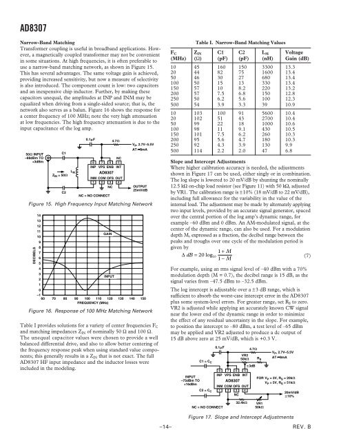
Narrow-Band Matching<br />
Transformer coupling is useful in broadband applications. However,<br />
a magnetically coupled transformer may not be convenient<br />
in some situations. At high frequencies, it is often preferable to<br />
use a narrow-band matching network, as shown in Figure 15.<br />
This has several advantages. The same voltage gain is achieved,<br />
providing increased sensitivity, but now a measure of selectivity<br />
is also introduced. The component count is low: two capacitors<br />
and an inexpensive chip inductor. Further, by making these<br />
capacitors unequal, the amplitudes at INP and INM may be<br />
equalized when driving from a single-sided source; that is, the<br />
network also serves as a balun. Figure 16 shows the response for<br />
a center frequency of 100 <strong>MHz</strong>; note the very high attenuation<br />
at low frequencies. The high frequency attenuation is due to the<br />
input capacitance of the log amp.<br />
50 INPUT<br />
–88<strong>dB</strong>m TO<br />
+3<strong>dB</strong>m<br />
C1<br />
Z IN = 50<br />
C2<br />
L M<br />
0.1F<br />
INP VPS ENB INT<br />
<strong>AD8307</strong><br />
4.7<br />
NC<br />
INM COM OFS OUT<br />
NC = NO CONNECT<br />
NC<br />
V P , 2.7V–5.5V<br />
AT 8mA<br />
OUTPUT<br />
25mV/<strong>dB</strong><br />
Figure 15. High Frequency Input Matching Network<br />
DECIBELS<br />
14<br />
13<br />
12<br />
11<br />
10<br />
9<br />
8<br />
7<br />
6<br />
5<br />
4<br />
3<br />
2<br />
1<br />
0<br />
GAIN<br />
INPUT<br />
–1<br />
60 70 80 90 100 110 120 130 140 150<br />
FREQUENCY (<strong>MHz</strong>)<br />
Figure 16. Response of 100 <strong>MHz</strong> Matching Network<br />
Table I provides solutions for a variety of center frequencies F C<br />
and matching impedances Z IN of nominally 50 Ω and 100 Ω.<br />
The unequal capacitor values were chosen to provide a well<br />
balanced differential drive, and also to allow better centering of<br />
the frequency response peak when using standard value components;<br />
this generally results in a Z IN that is not exact. The full<br />
<strong>AD8307</strong> HF input impedance and the inductor losses were<br />
included in the modeling.<br />
Table I. Narrow-Band Matching Values<br />
F C Z IN C1 C2 L M Voltage<br />
(<strong>MHz</strong>) (Ω) (pF) (pF) (nH) Gain (<strong>dB</strong>)<br />
10 45 160 150 3300 13.3<br />
20 44 82 75 1600 13.4<br />
50 46 30 27 680 13.4<br />
100 50 15 13 330 13.4<br />
150 57 10 8.2 220 13.2<br />
200 57 7.5 6.8 150 12.8<br />
250 50 6.2 5.6 100 12.3<br />
500 54 3.9 3.3 39 10.9<br />
10 103 100 91 5600 10.4<br />
20 102 51 43 2700 10.4<br />
50 99 22 18 1000 10.6<br />
100 98 11 9.1 430 10.5<br />
150 101 7.5 6.2 260 10.3<br />
200 95 5.6 4.7 180 10.3<br />
250 <strong>92</strong> 4.3 3.9 130 9.9<br />
500 114 2.2 2.0 47 6.8<br />
Slope and Intercept Adjustments<br />
Where higher calibration accuracy is needed, the adjustments<br />
shown in Figure 17 can be used, either singly or in combination.<br />
The log slope is lowered to 20 mV/<strong>dB</strong> by shunting the nominally<br />
12.5 kΩ on-chip load resistor (see Figure 11) with 50 kΩ, adjusted<br />
by VR1. The calibration range is ±10% (18 mV/<strong>dB</strong> to 22 mV/<strong>dB</strong>),<br />
including full allowance for the variability in the value of the<br />
internal load. The adjustment may be made by alternately applying<br />
two input levels, provided by an accurate signal generator, spaced<br />
over the central portion of the log amp’s dynamic range, for<br />
example –60 <strong>dB</strong>m and 0 <strong>dB</strong>m. An AM-modulated signal, at the<br />
center of the dynamic range, can also be used. For a modulation<br />
depth M, expressed as a fraction, the decibel range between the<br />
peaks and troughs over one cycle of the modulation period is<br />
given by<br />
1 + M<br />
∆ <strong>dB</strong> = 20 log 10<br />
(7)<br />
1 − M<br />
For example, using an rms signal level of –40 <strong>dB</strong>m with a 70%<br />
modulation depth (M = 0.7), the decibel range is 15 <strong>dB</strong>, as the<br />
signal varies from –47.5 <strong>dB</strong>m to –32.5 <strong>dB</strong>m.<br />
The log intercept is adjustable over a ±3 <strong>dB</strong> range, which is<br />
sufficient to absorb the worst-case intercept error in the <strong>AD8307</strong><br />
plus some system-level errors. For greater range, set R S to zero.<br />
VR2 is adjusted while applying an accurately known CW signal<br />
near the lower end of the dynamic range in order to minimize<br />
the effect of any residual uncertainty in the slope. For example,<br />
to position the intercept to –80 <strong>dB</strong>m, a test level of –65 <strong>dB</strong>m<br />
may be applied and VR2 adjusted to produce a dc output of<br />
15 <strong>dB</strong> above zero at 25 mV/<strong>dB</strong>, which is +0.3 V.<br />
INPUT<br />
–75<strong>dB</strong>m TO<br />
+16<strong>dB</strong>m<br />
0.1F<br />
4.7<br />
VR2<br />
R S<br />
C1 = C 50k<br />
C<br />
C2 = C C<br />
NC = NO CONNECT<br />
INP VPS ENB INT<br />
<strong>AD8307</strong><br />
INM COM OFS OUT<br />
NC<br />
32.4k<br />
3<strong>dB</strong><br />
V P , 2.7V–5.5V<br />
AT 8mA<br />
FOR V P = 3V, R S = 20k<br />
V P = 5V, R S = 51k<br />
VR1<br />
50k<br />
20mV/<strong>dB</strong><br />
10%<br />
Figure 17. Slope and Intercept Adjustments<br />
–14–<br />
REV. B