SESHA 2011 Program Book - Semiconductor Safety Association
SESHA 2011 Program Book - Semiconductor Safety Association
SESHA 2011 Program Book - Semiconductor Safety Association

Create successful ePaper yourself
Turn your PDF publications into a flip-book with our unique Google optimized e-Paper software.
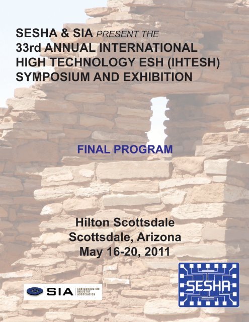
<strong>SESHA</strong> & SIA PRESENT THE<br />
33rd ANNUAL INTERNATIONAL<br />
HIGH TECHNOLOGY ESH (IHTESH)<br />
SYMPOSIUM AND EXHIBITION<br />
FINAL PROGRAM<br />
Hilton Scottsdale<br />
Scottsdale, Arizona<br />
May 16-20, <strong>2011</strong>
Vertex M_<strong>SESHA</strong> ad.indd 1<br />
4/11/<strong>2011</strong> 3:27:31 PM<br />
small is big<br />
Honeywell Analytics Vertex M packs the<br />
industry’s most reliable gas detection technology,<br />
colorimetric Chemcassette ® , into a smaller<br />
cabinet. Now you can pay dramatically less for<br />
the High Tech industry’s most renowned gas<br />
monitoring system.<br />
Big on performance, Vertex M with Chemcassette offers parts per billion detection<br />
of over 40 toxic gases, with proof of response to a gas release leaving an identifying<br />
stain on the Chemcassette tape. Big on value with an exceptional entry price, Vertex M<br />
reduces your monitoring cost per point and frees up precious floor space. With 8 to 24<br />
points of detection, Vertex M supports a range of installation options for fabs, research<br />
labs, chemical, photovoltaic, nano manufacturing and other High Tech applications —<br />
perfect for augmenting an existing gas monitoring system, upgrading to newer, more<br />
innovative technology, or trying a chemically imprinted paper for the first time. Big on<br />
support, Vertex M means you have Honeywell standing behind your investment with a<br />
big commitment including 24/7 field service availability and an expert customer support<br />
team. Honeywell Analytics. Experts in gas detection.<br />
For more information, visit vertexmbyhoneywell.com or call 1-800-538-0363.<br />
© <strong>2011</strong> Honeywell International Inc. All rights reserved.
<strong>SESHA</strong> 33rd Annual International High<br />
Technology ESH Symposium & Exposition<br />
Where ESH and Technologies Converge<br />
Table of Contents<br />
Week at a Glance (Committees, Events, Sessions) ....................................................................................2<br />
Professional Development Courses ...........................................................................................................3<br />
Planning Team/Board of Directors .............................................................................................................6<br />
Final <strong>Program</strong> ............................................................................................................................................7<br />
Speaker Biographies..................................................................................................................................25<br />
Exhibitors by Booth Number.....................................................................................................................33<br />
Hilton Scottsdale<br />
Scottsdale, Arizona<br />
Guest Phone: 480-948-7750<br />
Guest Fax: 480-948-2232<br />
Symposium attendees are eligible to receive certification<br />
maintenance points from both BCSP and ABIH.<br />
Certificates are available at the Registration Desk.<br />
Registration Hours:<br />
Salon I Foyer<br />
Monday, May 16 .................................................................................................................... 3:00-6:00 PM<br />
Tuesday, May 17 .............................................................................................................7:00 AM-6:00 PM<br />
Wednesday, May 18 .......................................................................................................7:30 AM-4:00 PM<br />
Thursday, May 19 ...............................................................................................................7:30 AM-Noon<br />
Exhibit Hall Hours:<br />
Salons I/II/III<br />
Tuesday, May 17..............................................................................................................9:30 AM-7:00 PM<br />
Break.........................................................................................................................9:30-10:00 AM<br />
Exhibitor Sponsored Lunch...................................................................................... Noon-1:45 PM<br />
Break ......................................................................................................................... 3:15-3:45 PM<br />
Tuesday, May 17 Opening Reception & Raffle Drawing....................................................... 5:15-7:00 PM<br />
Wednesday, May 18 ........................................................................................................9:00 AM-4:00 PM<br />
Break .......................................................................................................................9:30-10:00 AM<br />
Cash & Carry Lunch ........................................................................................ 11:30 AM-1:00 PM<br />
Break and Raffle Drawing.......................................................................................... 3:15-3:45 PM<br />
<strong>SESHA</strong> 33rd Annual International High Technology ESH Symposium & Exhibition<br />
1
Monday, 16 May<br />
Board of Directors<br />
1:00-5:00 pm Sonora D<br />
PDC 1-Fundamentals and EHS Challenges of <strong>Semiconductor</strong><br />
Manufacturing<br />
8:00 am-5:00 pm Sonora A<br />
PDC 2-Vacuum and Cryogen <strong>Safety</strong> Concerns<br />
8:00 am-Noon Sonora B<br />
PDC 3-Silane <strong>Safety</strong><br />
1:00-5:00 pm Sonora B<br />
PDC 4-Ethics and ESH<br />
6:00-8:00 pm Sonora B<br />
Tuesday, 17 May<br />
Opening Ceremony and Awards Presentation - <strong>SESHA</strong><br />
History Project, Liz Aton<br />
8:00-9:30 am Sonora A/B/C<br />
Break<br />
9:30-10:00 am Salons I/II/III<br />
Exhibits<br />
9:30 am-7:00 pm Salons I/II/III<br />
SIA Regional Updates - SIA, ESIA, TSIA, CSIA, KSIA,<br />
JSIA<br />
10:00-11:00 am Sonora A/B/C<br />
Keynote - Global <strong>Semiconductor</strong> Industry - Looking Forward,<br />
David Isaacs; SIA<br />
11:00 am-Noon Sonora A/B/C<br />
Complimentary Exhibitor Sponsored Lunch<br />
Noon-1:45 pm<br />
Week Schedule<br />
Salons I/II/III<br />
Concurrent Sessions<br />
1:45-3:15 pm Sonora A/B/C<br />
Break - Raffle Ticket Distribution<br />
3:15-3:45 pm Salons I/II/III<br />
Concurrent Sessions<br />
3:45-5:30 pm Sonora A/B/C<br />
Opening Reception - Raffle Ticket Drawing<br />
5:15-7:00 pm Salons I/II/III<br />
Wednesday, 18 May<br />
Exhibitor Breakfast<br />
7:30 am Salons I/II/III<br />
Keynote Presentation: IC Insights, Trevor Yancey<br />
8:30-9:30 am Sonora A/B/C/D<br />
Exhibits<br />
9:00 am-4:00 pm Salons I/II/III<br />
2<br />
Break - 2nd Raffle Ticket Distribution & Raffle Drawing<br />
9:30-10:00 am Salons I/II/III<br />
Concurrent Sessions<br />
10:00-11:30 am Sonora A/B/C/D<br />
Cash & Carry Lunch<br />
11:30 am-1:00 pm Salons I/II/III<br />
Concurrent Sessions<br />
1:00-3:15 pm Sonora A/B/C/D<br />
Break - Raffle Ticket Distribution & Raffle Drawing<br />
3:15-3:45 pm Salons I/II/III<br />
Concurrent Sessions<br />
3:45-5:30 pm Sonora A/B/C<br />
Thursday, 19 May<br />
5K Race<br />
6:30 am Meet in Lobby<br />
Fellows Breakfast<br />
7:30-8:00 am Sonora D1<br />
Region Chapter Leader Breakfast<br />
7:30 am Salon 4<br />
Keynote - Towards Harmonization of Measuring and<br />
Reporting Product Sustainability, Kevin Dooley<br />
8:30-9:30 am Sonora A/B/C<br />
Break<br />
9:30-10:00 am Sonora Foyer<br />
Concurrent Sessions<br />
10:00-11:30 am Sonora A/B/C<br />
Lunch on your Own<br />
11:30 am-1:00 pm X<br />
Concurrent Sessions<br />
1:00-3:15 pm Sonora A/B/C<br />
Break<br />
3:15-3:45 pm Sonora Foyer<br />
Closing Ceremony & Prize Drawing<br />
3:45-5:00 pm Sonora A/B/C<br />
Board of Directors<br />
5:00-6:00 pm Sonora D<br />
Friday, 20 May<br />
PDC 5-Fundamentals & EHS Challenges of PV Manufacturing<br />
8:00 am-5:00 pm Salon I<br />
PDC 6-Exhaust Management, Point-of-Use Abatement Devices,<br />
Electronics Industry Greenhouse Gas Reporting Rule,<br />
and Process Emissions and POU Abatement Device DRE/<br />
Emissions Testing Methodologies<br />
8:00 am-5:00 pm Salon II
Professional Development Courses<br />
Monday 16 May - Friday 20 May<br />
Monday 16 May<br />
Full Day, 8:00 am – 5:00 pm<br />
PDC1 Fundamentals and ESH Challenges of<br />
<strong>Semiconductor</strong> Manufacturing - Sonora A<br />
Susan Creighton<br />
The <strong>2011</strong> Introduction to <strong>Semiconductor</strong> ESH<br />
class is intended for ESH students and professionals<br />
new to the semiconductor industry and operations. Topics<br />
covered in the class include: •An overview of the<br />
semiconductor industry and operations •A virtual tour<br />
of a semiconductor fab •An introduction to the semiconductor<br />
manufacturing process •A presentation on occupational<br />
health and safety issues in a semiconductor<br />
fab •A review of semiconductor environmental considerations<br />
•Discussions on SEMI EHS Standards: S2, S8<br />
and S23 •A summary of global environmental regulations.<br />
An experienced semiconductor EHS professional<br />
recognized in their area of expertise presents each topic.<br />
This will be a full day PDC. Students will be provided<br />
with handouts of each presentation.<br />
3<br />
Half Day, 8:00 am - Noon<br />
PDC2 Vacuum and Cryogen <strong>Safety</strong> Concerns<br />
for Laboratory Applications - Sonora B<br />
Roger Shrouf<br />
Vacuum systems can present a variety of hazards<br />
to the laboratory worker. This course will provide an indepth<br />
discussion of a wide variety of hazards and mitigation<br />
techniques related to vacuum systems in a research<br />
laboratory environment. A thorough discussion of the<br />
interface between the vacuum system and commonly<br />
associated pressure sources (such as backfill or process<br />
gases) will be provided. The limitations and safety<br />
concerns associated with vacuum purging of associated<br />
pressure systems will be included. Potential accidental<br />
overpressure of the vacuum system will be emphasized<br />
as well as safety concerns for the use of brittle materials<br />
in vacuum applications. Course discussions will also include<br />
ancillary hazards commonly associated with vacuum<br />
applications such as vacuum pump issues, electrical<br />
safety hazards, and mechanical concerns. Many vacuum<br />
processes involve the use of cryogenic fluids – and<br />
nearly all cryogenic fluid applications involve the use of<br />
vacuum. Therefore, cryogenic fluid properties and hazards<br />
as well as mitigation techniques will be discussed.<br />
The primary focus of the cryogen safety segment of the<br />
course will be on liquid nitrogen and liquid helium applications.<br />
A wide variety of hazards will be discussed<br />
including the highlighted hazards of pressure build up<br />
from the warming of trapped cryogens and asphyxiation<br />
concerns. The features and safety concerns of cryogenic<br />
liquid Dewars will also be illustrated. Open discussion<br />
will be encouraged throughout the course and lessons<br />
learned from accident scenarios will be included where<br />
applicable.<br />
Half Day, 1:00 – 5:00 pm<br />
PDC3 Silane <strong>Safety</strong> - Sonora B<br />
Eugene Ngai<br />
Unpredictable, delayed ignition and explosive are<br />
words typically used to describe the behavior of silane.<br />
Since 2006 significant attention has been focused on<br />
silane safety because of the increasing number of incidents.<br />
One day safety seminars and training classes have<br />
been conducted around the world by leading experts.<br />
Despite these efforts, silane related incidents continue to<br />
occur worldwide. Attend this Professional Development<br />
Course and you will learn the latest on silane from leading<br />
experts. Agenda items include review of the history<br />
of silane, how it behaves, insurance/industry funded research<br />
projects and their importance of how silane systems<br />
can be designed to drastically reduce the number<br />
of incidents and/or their severity. A code overview and<br />
best practices for silane handling will also be presented.<br />
1:00 – 1:15 Eugene Ngai: Welcome and Introductions<br />
1:15 – 1:45 Eugene Ngai: Review of recent incidents<br />
1:45– 2:30 John Cox and Beth Tshudy: Code Case Study<br />
2:30 – 3:00 Crystal Mjelde: Bulk Installations<br />
3:00 – 3:15 Break<br />
3:15 – 3:45 Sue Creighton: Abatement<br />
3:45 – 4:15 Eugene Ngai: Testing and G13<br />
4:15 – 4:50 Vinnie DeGiorgio: Best Practices<br />
4:50 – 5:00 Closing remarks<br />
Evening, 6:00 – 8:00 pm<br />
PDC4 Nanoethics: <strong>Safety</strong>, Risk, and Responsible<br />
Innovation - Sonora B<br />
Sarah Davies<br />
This session offers an introduction to contemporary<br />
thinking on nanoethics, applying this to the context<br />
of the industrial laboratory and opening up a discussion<br />
of what constitutes ethical practice in scientific research<br />
and development. Throughout, the emphasis will be on<br />
the critical skills and tools needed to engage in informal<br />
ethical reflection in the workplace. After giving a
whirlwind tour of key ideas in nanoethics, the focus will<br />
move to ways in which the ‘ethical’ is being used within<br />
notions of responsible innovation and corporate social<br />
responsibility. The continuum between ‘doing no harm’<br />
and being a ‘positive social force’ will be introduced,<br />
with reference to what this continuum will look like in<br />
the context of the industrial hygiene and safety professions.<br />
Recent research on lay ethical concerns regarding<br />
nanotechnology will also be discussed. Finally, the<br />
group will engage in a discussion of how ‘nanoethics’<br />
can be practically applied to the professional contexts<br />
in which they work. This course is coordinated by Dr<br />
Sarah R Davies, of the Center for Nanotechnology in<br />
Society at Arizona State University.<br />
Friday 20 May<br />
Full Day, 8:00 am – 5:00 pm<br />
PDC5 Fundamentals and EHS Challenges of<br />
PV Manufacturing - Salon I<br />
PDC Facilitator: Andrew McIntyre, CIH and Managing<br />
Principal - EORM<br />
PDC Presenters: EHS and Sustainability experts<br />
from various companies involved in the manufacture of<br />
Photovoltaics as well as the Solar Energy Industry <strong>Association</strong><br />
representatives.<br />
Abstract: Photovoltaic (PV) technologies provide<br />
energy with distinct environmental benefits over traditional<br />
energy generating technologies, which have given<br />
the PV industry a strong reputation as a “green industry.”<br />
With the rapid increase in demand (both consumer<br />
and commercial) for PV products, it is essential that the<br />
PV industry fulfill the promise of being a green industry<br />
by avoiding many of the past environmental, health &<br />
safety (EHS) pitfalls encountered during the expansion<br />
of similar high-technology industries. Experience with<br />
the semiconductor industry over the last three decades<br />
has provided a clear EHS roadmap for the PV industry<br />
to follow. This professional development course will<br />
provide specific details on the EHS and sustainability<br />
hazards/controls of the solar cell and module manufacturing,<br />
installation, maintenance and end-of-life product<br />
issues.<br />
Who Should Attend: This PV Professional Development<br />
Course is intended for conference participants<br />
interested in learning more about the hazards, hierarchy<br />
of risk controls and current EHS and Sustainability challenges<br />
facing the manufacturers of photovoltaic products.<br />
PDC Agenda<br />
Welcomes, Introduction and Course Objectives<br />
Andrew McIntyre, CIH - Managing Principal - Environmental<br />
& Occupational Risk Management, Inc. (EORM)<br />
Key Note - Global Regulatory Drivers and Challenges<br />
Lisa Krueger - Vice President of Sustainability - First<br />
Solar<br />
Solar Energy Industry <strong>Association</strong> (SEIA) EHS Initiatives<br />
Christine Covington - Manager of Government Affairs;<br />
Environment, Health, & <strong>Safety</strong> - Solar Energy Industries<br />
<strong>Association</strong> (SEIA)<br />
Industrial Hygiene, <strong>Safety</strong>, Fire Protection and Environmental<br />
Risk Considerations and Controls (Speakers<br />
from the following Crystalline and Thin Film Process<br />
Manufacturers)<br />
Crystalline PV - Jim Larson - EHS Manager, SunPower<br />
Cadmium Telluride(CdTe) PV - Ken Smigielski - EHS<br />
Engineering Group, First Solar<br />
Copper, Indium, Gallium Selenide (CIGS) PV - TBD<br />
High Efficiency Multijunction Concentrator Cell PV -<br />
Holly Baez, EHS Manager, Spectrolab, a Boeing Company<br />
Corporate Social Responsibility - Challenges and Opportunities<br />
for the PV Industry<br />
Todd Brady - Global Environmental Manager - Intel<br />
Corporation<br />
Supply Chain Management<br />
Leann Speta - Supply Chain Sustainability Manager -<br />
SunPower Corporation<br />
Installer EHS Considerations - Residential, Industrial,<br />
and Solar Farm/Utility Level<br />
TBD<br />
Recycling Processes & End-of-Life Considerations<br />
Jennifer Woolwich, MA, CPHQ, CSSBB - CEO - PV Recycling,<br />
LLC<br />
PDC6 Exhaust Management, Point-of-Use<br />
Abatement Devices, Electronics Industry Greenhouse<br />
Gas Reporting Rule, and Process Emissions<br />
and POU Abatement Device DRE/Emissions Testing<br />
Methodologies - Salon II<br />
Mike Sherer<br />
<strong>Semiconductor</strong> process and fab exhaust management<br />
procedures and strategies will be presented. Many<br />
of these also apply to LCD, solar and related industries.<br />
Discussion of fluorine, particulate, ammonia and ozone<br />
4
will be highlighted. Point-of-Use (POU) abatement technologies<br />
overview will be provided. Important items to<br />
assist personnel in reducing maintenance and increasing<br />
uptime will detailed. The EPA Greenhouse Reporting<br />
Rule for electronics industry will be presented and any<br />
lessons learned provided. The EPA Testing Protocol for<br />
POU abatement device Destruction and Removal Efficiency<br />
(DRE) and the 2009 ISMI Testing Guideline will<br />
be presented. This overview will allow the attendee to<br />
understand how testing is conducted and how to work<br />
with testing suppliers.<br />
5
Symposium Planning Committee:<br />
Co-Chairs: Steve Trammell, Laurie Beu,<br />
Tom Diamond and David Isaacs<br />
PDC<br />
Co-Chairs: Laurie Beu, Susan Creighton and<br />
Dawn Speranza<br />
Keynote Speaker Coordinators<br />
Co-Chairs: Vinnie DeGiorgio, David Isaacs and<br />
Kimberly Smieja<br />
Global Chemical Regulations Session<br />
Chair: Tim Yeakley<br />
<strong>Safety</strong>/IH Session<br />
Co-Chairs: John Bucciarelli, Kim Smieja<br />
Greenhouse Gas Session<br />
Co-Chairs: Brett Davis, Hilary Matthews<br />
Corporate Social Responsibility Session<br />
Chair: Bonnie Peralta<br />
Symposium Planning Team<br />
Photovoltaic ESH Session<br />
Chair: John Cox<br />
Emerging Codes and Regulations Session<br />
Chair: Tiffany Giles<br />
Waste Minimization Session<br />
Chair: Jennifer Chittick<br />
Disaster Preparedness Round Table<br />
Chair: Vinnie DeGiorgio<br />
Abatement Strategies Session<br />
Chair: Dale Moore<br />
Risk Management Session<br />
Co-Chairs: Andy McIntyre, Pat Tierney<br />
Energy Conservation Session<br />
Chair: Doug Thornton<br />
Executive Committee<br />
President – Karl Albrecht,<br />
Fairchild <strong>Semiconductor</strong> Corp<br />
President-Elect – Kimberly Smieja, Intel Corporation<br />
Past-President – Paul M. Connor,<br />
Dow Electronic Materials<br />
Treasurer – Steve Roberge, Axcelis<br />
Secretary – Doug Thornton,<br />
Fairchild <strong>Semiconductor</strong> Corp<br />
Executive Director – Brett Burk<br />
Board of Directors<br />
Board of Directors<br />
Sanjay Baliga, SEMI<br />
Jennifer Chittick, BAE Systems<br />
John D. Cox, Advanced Technology Solutions<br />
Vincent A. DeGiorgio, FM Global<br />
Thomas Diamond, <strong>Semiconductor</strong> Industry Assoc.<br />
Dawn Speranza, Intel Corporation<br />
Steven Trammell, ISMI<br />
John Visty, Salus Engineering International<br />
Mary Majors, Editor, Air Products & Chemicals Inc<br />
6
Tuesday<br />
8:00-9:30 am<br />
Opening Ceremony and<br />
Awards Presentation<br />
Sonora A/B/C<br />
10:00-11:00 am<br />
SIA Regional Updates<br />
Sonora A/B/C<br />
11:00 am-Noon<br />
Keynote - Global <strong>Semiconductor</strong><br />
Industry - Looking Forward<br />
Sonora A/B/C<br />
Noon-1:45 pm<br />
Final <strong>Program</strong><br />
Lunch Break, Exhibit Hall<br />
1:45-4:30 pm<br />
Global Chemical Regulations<br />
Sonora A<br />
1:45 pm Environmental Regulatory Developments<br />
in the EU<br />
Harte, S; ESIA - European <strong>Semiconductor</strong> Industry <strong>Association</strong>,<br />
Belgium<br />
ISESH <strong>2011</strong> / <strong>SESHA</strong> 33rd Annual ESH Symposium<br />
Abstract Title : Environmental Regulatory Developments<br />
in the European Union Substance restrictions<br />
or substance related bans on use are an obvious point of<br />
concern for many sections of the high tech sector. They<br />
are however not something new for the worldwide semiconductor<br />
manufacturing supply chain. Nevertheless the<br />
restriction of substances whether through EU RoHS or<br />
REACH systems will continue into the forseeable future.<br />
In addition the industry needs to prepare activity<br />
and roadmap plans to move away from the exempted<br />
substance and applications where possible to do so.<br />
This presentation will be broad ranging in nature and<br />
aim to update the conference on the regulatory developments<br />
in Europe in terms of substances restrictions<br />
through REACH, EU RoHS or potentially PFOA and<br />
the evolution of potential revised flourinated gas regulations<br />
within the EU in <strong>2011</strong> and will assess the impact<br />
on semiconductor industries. The presentation will also<br />
outline the revised exemption review systems under the<br />
revised RoHS directive.<br />
7<br />
2:30 pm JAMP Activity Update<br />
Ibuka, S; Tokyo Electron Limited<br />
JAMP means “Joint Article Management Promotion”<br />
council for cross-industry. JAMP frmawork is<br />
applicable to chemical/subsatance information transfer<br />
through whole supply chain globally, which are required<br />
by EU REACH, EU CLP, each country’s GHS,<br />
US TSCA or many international/local legslation. JAMP<br />
was introduced at the last IHTESH held in Taiwan. Currently,<br />
JAMP is introduced in ISO26000 and the draft of<br />
ECHA REACH guidance. JAMP activity update should<br />
be presented there.<br />
3:15 pm Break & Raffle Distribution, Exhibit Hall<br />
3:45 pm Decontamination and Decommissioning<br />
of Equipment: Roundtable Discussion<br />
Yeakley, T; Texas Instrumentsu<br />
<strong>Semiconductor</strong> manufacturing and research facilities<br />
regularly ship equipment parts for rebuild or repair.<br />
These parts could contain chemical and byproducts residues<br />
that cannot be removed on-site without causing<br />
irreversible damage to the part. The presence of these<br />
residues may also require compliance with various regulations<br />
during transport from DOT, IATA, IMDG, etc.<br />
The purpose of this roundtable discussion is to share<br />
information between semiconductor companies on the<br />
best known methods to classify these parts for transportation.<br />
We will discuss how to determine whether decontamination<br />
of a specific part onsite is appropriate; the<br />
de-minimus quantities above which the part will have to<br />
be regulated; methods used to determine the hazards of<br />
byproducts in parts; necessity of testing the byproducts;<br />
whether regulatory tests can be modified for practical<br />
application; and methods for managing special cases<br />
like batteries and magnets.<br />
1:45-5:15 pm<br />
<strong>Safety</strong>-IH<br />
Sonora B<br />
1:45 pm Evaluation of Potential Cytotoxicity of<br />
Nanoscale Inorganic Oxides Utilized in <strong>Semiconductor</strong><br />
Manufacturing<br />
Sierra-Alvarez, R, Otero, L, Garcia, C, Luna-Velasco, A,<br />
Cobo, A, Field, JA; University of Arizona, Tucson<br />
The future success of the semiconductor industry<br />
is dependent on the capacity to manufacture smaller<br />
and smaller devices which requires the use of nanopar-
ticles (NPs). Numerous reports have been published in<br />
recent years expressing concern for the potential toxicity<br />
of NPs to humans and ecologically important species.<br />
The objective of this work was to investigate the<br />
potential cytotoxicity of nanoscale inorganic oxides<br />
commonly utilized in semiconductor manufacturing<br />
(SiO2, Al2O3, CeO2) and emerging inorganic oxide<br />
nanoparticles (HfO2). Other commercially-important<br />
inorganic oxides (ZnO, TiO2, ZrO2, Mn2O3) were also<br />
included in the study for comparison. Nanotoxicity was<br />
assessed using several well-established bioassays (e.g.,<br />
Microtox, yeast respiration measurements, MTT) and<br />
a recently developed impedance-based Real Time Cell<br />
Assay (RTCA). The target cells in those bioassays included<br />
bacteria, yeast, and human cells. Additional assays<br />
were performed to evaluate the potential involvement<br />
of reactive oxygen species (ROS), toxic soluble<br />
species, and/or decrease in cell membrane integrity on<br />
cytotoxicity. Furthermote, the particle size distribution<br />
and fraction of inorganic oxide effectively dispersed in<br />
the various bioassay media was investigated in order to<br />
get information on the actual hydrodynamic diameter<br />
and state of dispersion of the nanomaterials. With the<br />
exception of SiO2 which formed highly stable dispersions,<br />
the nanoscale inorganic oxides tested showed a<br />
high tendency to aggregate in most biological media resulting<br />
in micron-size aggregates that settled out of the<br />
dispersion. ZnO and Mn2O3 were the most inhibitory<br />
inorganic oxide nanomaterials evaluated with 50% inhibiting<br />
concentrations often in the low ppm range. In<br />
contrast, CeO2 and HfO2 were nontoxic in most assays<br />
at concentrations as high as 1,000 mg L-1. Nanosized<br />
SiO2 and Al2O3 showed intermediate to low cytotoxicity.<br />
The underlying mechanisms involved in the cytotoxicity<br />
of these nanomaterials are currently under investigation.<br />
Furthermore, the results obtained indicated the<br />
potential of impedance based RTCA to rapidly screen<br />
for nanoparticle toxicity. Future research will address<br />
validation of the RTCA results using conventional cytotoxicity<br />
tests.<br />
8<br />
2:30 pm Preventing Musculoskeletal Discomforts<br />
for a Healthy Workplace<br />
Lin, R-T; Taiwan <strong>Semiconductor</strong> Manufacturing Company,<br />
Taiwan<br />
Musculoskeletal diseases are on top, accounting<br />
for 73%, of the ranking of compensated occupational<br />
diseases in 2010 in Taiwan. Previously reported musculoskeletal<br />
discomforts among fabrication room (fab)<br />
workers were owing to frequent manual wafer pod handling<br />
or operating manufacturing equipments with improper<br />
anthropometric data for users in different countries.<br />
In addition, sufferers of work-related tendinitis are<br />
entitled to compensation since 2010 under the new list<br />
of occupational diseases in Taiwan, leading to an anticipated<br />
soar of work-related musculoskeletal diseases<br />
compensation due to long hours of use or repetitive typing<br />
among computer users. Providing an ergonomic<br />
working interface for a company with hundreds of thousands<br />
workers is a challenge to balance the purchase<br />
specification and cost. Under the changing working<br />
interface from on-site process equipment operation to<br />
remote computer monitoring, the report aims to provide<br />
an overview of prevalent trends, regulatory standards,<br />
and challenges of musculoskeletal disease among different<br />
countries. The report demonstrates our systematic<br />
approach for reducing workers’ awkward postures and<br />
musculoskeletal complaints through ergonomically redesigned<br />
fab/office workstations. In addition to statistical<br />
data, the report also includes an introduction of health<br />
care programs on solving musculoskeletal discomforts,<br />
such as massage and traditional Chinese medicine lectures.<br />
Information on the effectiveness of ergonomic<br />
programs has been computerized and integrated into e-<br />
ESH system. Our case studies and experience sharing<br />
may be of use in both policy and practice for reducing<br />
ergonomics-related occupational diseases and promoting<br />
a healthier workplace.<br />
3:15 pm Break & Raffle Distribution, Exhibit Hall<br />
3:45 pm Tetramethylammonium Hydroxide<br />
(TMAH): Toxicity and Methods to Reduce Risk in<br />
the Workplace<br />
DiZio, K, Melville, R, Timlin, E; IBM, San Ramon, CA<br />
and Hopewell Junction, NY<br />
Tetramethylammonium hydroxide (TMAH), CAS<br />
#75-59-2, is employed in an increasing number of semiconductor<br />
manufacturing processes. Newer applications<br />
may use TMAH concentrations as high as 25% at elevated<br />
temperatures. Contact with concentrated TMAH<br />
solutions may cause serious intoxication. Several fatalities<br />
have been reported by the Asia Pacific semiconductor<br />
and photoelectric industries. Factors that may<br />
be important in determining the degree of intoxication<br />
include the concentration of TMAH, the % body surface<br />
area affected, the period before decontamination, and<br />
the possibility of concurrent inhalation exposure and<br />
dermal contact. Early toxicity studies in rats and guinea<br />
pigs identified TMAH as highly toxic with an oral LD50<br />
in rats between 34 and 50 mg/kg and a dermal LD50<br />
in guinea pigs of 25 to 50 mg/kg. Later studies in rats
sponsored by IBM found that contact with less than 1<br />
milliliter of a 12% or 25% TMAH solution was lethal<br />
within 3 hours. IBM investigated possible underlying<br />
mechanisms of acute systemic toxicity including the direct<br />
effects on neurotransmission and on blood gases.<br />
IBM took prompt action to assess and, where necessary,<br />
enhance the health and safety procedures associated<br />
with TMAH based on the results of these animal studies.<br />
IBM notified the US EPA under the significant new<br />
information provisions of the Toxic Substances Control<br />
Act, Section 8e. Furthermore, IBM modified internal<br />
chemical labels for formulations containing TMAH,<br />
sponsored chemical-resistant glove and coverall permeation<br />
testing on TMAH solutions, performed process<br />
reviews on specific TMAH-using operations, and notified<br />
employees and contractors of the potential hazard.<br />
IBM implemented vigorous controls on the introduction<br />
of new processes employing concentrated TMAH<br />
solutions. Senior management is briefed on the potential<br />
hazards of the process, the tool and engineering<br />
requirements, and the availability of potential alternatives<br />
to TMAH. IBM develops work plans to reduce or<br />
eliminate potential TMAH hazards. In addition, IBM is<br />
working in cooperation with several development partners<br />
and suppliers to identify less hazardous alternatives<br />
to TMAH.<br />
4:30 pm The Integration of a Toxic Gas Monitoring<br />
System into the Building Fire Alarm System<br />
Sweeney, J; Harvard University<br />
Many facilities have toxic gas monitoring systems<br />
(TGMS) with local strobes to evacuate just clean rooms<br />
and affiliated areas. However, many facilities do not integrate<br />
their toxic gas monitoring systems into the building<br />
fire alarms systems. This presentation will describe<br />
three different types of toxic gas monitoring systems in<br />
a university setting and will describe how all three systems<br />
are integrated into the perspective building fire alarm<br />
systems. Topics of interest in this presentation will be as<br />
follows: 1. Details on TGMS Alarm level set points for<br />
exhaust and ambient gas sensors and when they trigger<br />
the building fire alarm systems; 2. Overview of how the<br />
two systems are integrated 3. Reasons for integrating the<br />
two systems; 4. Training details for all personnel involved<br />
in this new integrated system. In a university setting, the<br />
various working groups involved during emergencies<br />
are more expansive than in an industry setting. Types of<br />
people trained on the system (campus police, local fire<br />
fighters, facilities personnel, university operations center<br />
(24/7 hotline), EH&S department responders, building<br />
occupants etc).<br />
9<br />
1:45-5:15 pm<br />
GHG<br />
Sonora C<br />
1:45 pm Compliance Techniques for New Greenhouse<br />
Gas Regulations<br />
Higgs, T; Intel<br />
New greenhouse gas regulations pertaining to<br />
emissions reporting and facility permitting will impose<br />
multiple new requirements on semiconductor manufacturers<br />
and others in the electronics industries. The mandatory<br />
reporting rule for additional sources of fluorinated<br />
greenhouse gases (40CFR Part 98, subpart I) will<br />
require new approaches for measuring emissions, tracking<br />
inventories of fluorinated gases and heat transfer fluids,<br />
and add extensive new recordkeeping and reporting<br />
requirements. The Prevention of Significant Deterioration<br />
and Title V Greenhouse Gas Tailoring Rule (40CFR<br />
Parts 51, 52, 70 et. al.) will subject many sources to major<br />
source permitting requirements that have previously<br />
been able to avoid such requirements. These sources are<br />
likely to experience greatly increased requirements to<br />
understand and manage emissions impacts of routine<br />
changes, and significantly increased monitoring, reporting<br />
and recordkeeping burden. This presentation will<br />
examine compliance techniques for meeting the new<br />
requirements, and possible approaches for reducing the<br />
burden.<br />
2:30 pm PFC Stack Emissions Testing<br />
Inloes, S; WaferTech<br />
The goal of this testing was to determine if stack<br />
testing could be used to replace recipe specific testing<br />
required in the federal reporting rule. During February<br />
of <strong>2011</strong>, the SIA stack testing subcommittee developed<br />
the various stack testing options for testing emissions<br />
from electronic manufacturing Fabs. Various test methods<br />
were considered with the criteria determined to be<br />
1-10 ppb detection level . This equated to Fab emission<br />
of 1,000 to 40,000 MT CO2 eq depending on the Fab’s<br />
exhaust rate. Our site used GM/MS method to determine<br />
the concentrations of PFC’s and collection the samples<br />
using Summa containers. This method requires one-two<br />
days of onsite sample collection by a local emission testing<br />
company. Our process PFC emissions are routed to<br />
five acid scrubber stacks. In April of <strong>2011</strong>, we tested<br />
the five acid scrubbers simultaneously to reduce any<br />
variability of the site wide data. During the collection<br />
of the samples daily PFC gas usage data was collected<br />
and tier 2 emissions were compared to stack test results.
The daily rate was also compared to the prior year’s usage<br />
rate to determine if the test was representative of<br />
the annual usage rate. The GC/MS analyst was done at<br />
a remote certified lab with additional QC procedures<br />
to validate the method. The testing included duplicate<br />
samples, blanks, ambient samples, and spiked samples.<br />
These samples are also part of a stability study. The laboratory<br />
results demonstrate that the samples are accurate,<br />
stable and reproducible. The process data indicates<br />
that the tests were done while the plant was operating a<br />
90-110% of the annual PFC gas usage rate compared to<br />
the prior year. Part of the cost of the study was paid for<br />
by ISMI.<br />
3:15 pm Break & Raffle Distribution, Exhibit Hall<br />
and the non-confidential information available will be<br />
shared for this presentation. Members of the semiconductor<br />
industry desire to use this stack testing methodology<br />
to develop facility wide emissions factors for each<br />
GHG so that semiconductor fab GHG emissions can be<br />
estimated in a more accurate and cost effective manner.<br />
4:30 pm Staying Up to Date with the EPA’s Mandatory<br />
Reporting for Greenhouse Gases and California’s<br />
AB32- Regulations as They Relate to <strong>Semiconductor</strong><br />
and Related Devices<br />
Cook, J; EORM, San Jose CA<br />
This talk will provide an overview of the EPA and<br />
the California Air Resources Board (CARB) GHG regulations<br />
as they relate to the <strong>Semiconductor</strong>, LCD and PV<br />
manufacturing industries. The presentation will provide<br />
a brief regulatory update on significant international, national<br />
and state issues concerning climate change and<br />
highlight specific best practices, tools, strategies and<br />
lessons learned following the March 1, <strong>2011</strong> CARB<br />
compliance deadline. The presentation will conclude<br />
with a brief look forward on what the future may hold<br />
for GHG management in the technology sector.<br />
3:45 pm Developing a Fluorinated Greenhouse<br />
Gas Stack Testing Method Using FTIR<br />
Gilliland, T, Laush, C; Texas Instruments, Inc., IMACC<br />
Texas Instruments Incorporated (TI) is interested<br />
in identifying an alternative method to more accurately<br />
estimate Greenhouse Gas (GHG) emissions from their<br />
semiconductor fabrication operations(fabs) to reduce<br />
the cost burden of the final Mandatory Reporting Rule,<br />
Subpart I (40CFR98). In order to accomplishment this<br />
5:15-7:00 pm<br />
goal, TI proposes estimating emissions using a facility<br />
wide mass balance approach based on emissions characterization<br />
using familiar analytical equipment such<br />
Drawing<br />
Opening Reception & Raffle<br />
as the Fourier Transform InfraRed mass spectrometer<br />
(FTIR) and production metrics. Historical data using<br />
Salons I/II/III<br />
FTIR at the end of line exhaust stacks indicated that<br />
many of the process greenhouse gas (GHG) concentrations<br />
were below typical FTIR detection limits of 50<br />
Wednesday<br />
8:30-9:30 am<br />
parts per billion by volume (ppbv). IMACC, a company<br />
that specializes in designing and manufacture of FTIR<br />
Keynote<br />
monitoring systems for industry and government, understood<br />
the challenges of measuring these compounds at<br />
Sonora A/B/C/D<br />
8:30 am IC Insights<br />
sub-ppbv levels and performed experiments in their lab<br />
Yancey, T<br />
with a modified FTIR to achieve lower detection limits.<br />
The primary objective of this study was to measure in<br />
the field exhaust stacks at a typical operating semiconductor<br />
9:30 am Break, Exhibit Hall<br />
fab to demonstrate the feasibility of measuring<br />
10:00-11:30 am<br />
GHGs at sub-ppbv. IMACC, using their enhanced FTIR<br />
and approved EPA Methods 301 and 320, successfully<br />
<strong>Safety</strong>/IH<br />
measured stack level emissions at three TI fabs with detection<br />
Sonora A<br />
limits in the parts per trillion by volume (pptv), 10:00 am <strong>Safety</strong> and Health Committee<br />
thus demonstrating the feasibility at both 200mm and Qaio, X; Hynix <strong>Semiconductor</strong> (China) Ltd.<br />
300mm semiconductor fabs. The second objective of Hynix semiconductor China Limited (HSCL),<br />
this study was to reasonably correlate the semiconductor<br />
headquartered in Icheon, South Korea, is a wholly<br />
fab operational parameters with measurements at the foreign-owned enterprise located in Export Processing<br />
exhaust stack. The field data is currently being evaluated Zone Wuxi, Jiangsu province of China. HSCL’s main<br />
10
product is 12-inches wafer, and it covers an area of 54<br />
million square meters, of which the gross Investment<br />
reaches to 5.26 billion dollars. About 3700 employees<br />
from Korea and China work for HSCL.<strong>Safety</strong> and Health<br />
Committee <strong>Safety</strong> and Health committee is a communication<br />
bridge between employee and employer, created<br />
by Hynix and Hynix labor union together for the purpose<br />
of promoting mutual understanding between the<br />
labor and the capital, dissolving and improving internal<br />
issues of environmental, health and safety related to employees,<br />
making the optimal working environment for<br />
employees. Specificity 1. Specialty As far as the organization<br />
structure is concerned, <strong>Safety</strong> and Health committee<br />
is a newborn thing. Similar organization structure<br />
has not been found by now in other related industry. 2.<br />
Innovation In a point of view of foreign labor unions’<br />
operating mode, there is a sharp contradiction in terms<br />
of interests between labor union and enterprises. But the<br />
Hynix labor union is designed to protect and coordinate<br />
the interests of both sides of labor and capital, satisfy<br />
the employees and promote the enterprise development<br />
as well. Operation Overview 1.Organization Chairman<br />
of a committee; Chinese labor union chairman, Korean<br />
deputy general manager Committee member; Korean<br />
leaders from manufacturing department, technology<br />
department, general affairs department, and personnel<br />
labor union committee Executive:Responsible persons<br />
from ESH department 2.Operation Mode: Practical<br />
meeting: We collect advice and suggestions monthly<br />
from the basic level by various means and hold the practice<br />
meeting to take them over in the end/beginning of<br />
a month. Solutions will be taken out and significant issues<br />
would be submitted to periodic meeting for further<br />
discussion.Periodic meeting:Periodic meeting is held<br />
quarterly to debrief the results of practical meeting and<br />
provide advice and solutions to significant issues. 3.Operation<br />
Content: <strong>Safety</strong>: Clean room odor, PPE, toxic<br />
gas monitoring Environment: Dorm odor, corporate<br />
environment, sewage treatment Occupational health:<br />
noise, psychological consult, smoking and drinking, individual<br />
radiation dosimeter 4.Operation results <strong>Safety</strong><br />
and Health Committee has collected and disposed more<br />
than 200 advice and suggestions from 2008. Our operating<br />
environment and the safety consciousness of workers<br />
has been greatly improved. And the sense of trust<br />
between labor and capital has been enhanced a lot as<br />
well. As a result, our employees put more energy into<br />
production, makes more output and profit. In 2010, We<br />
Hynix got the historically highest profits.<br />
10:45 am A Study on Odor Reduction for <strong>Semiconductor</strong><br />
Industry<br />
Park, NH, Kim, SG, Shin, CS; Hynix <strong>Semiconductor</strong>,<br />
Repulic of Korea<br />
A Study On Odor Reduction for <strong>Semiconductor</strong><br />
Industry No-Hyeok Park, Sung-Gon Kim, Chong-Su<br />
Shin Cheong-Ju ESH Team, Administrtion Division,<br />
Hynix <strong>Semiconductor</strong> Inc. 1,55,125 Hyangjeong-dong<br />
Hungduk-gu Cheongju 361-725 Repulic of Korea Tel<br />
: 82-43-280-2615, Fax : 82-43-280-2489, E-mail : nohyuck.park@hynix.com<br />
Odor is caused by one or more<br />
volatilized chemical compounds that human being can<br />
perceive by the sense of olfaction and can feel unpleasant<br />
and disgusted. It is one kind of sensory pollution that<br />
results in physical and psychological harm. Especially,<br />
semiconductor industry have had difficulty in managing<br />
unclear odor as air pollutants generated by many<br />
kinds of gasesous chemical compounds and considering<br />
reduction measures. Hynix <strong>Semiconductor</strong> Inc. judged<br />
that odor problems will be issued by residents because<br />
the residential areas have been created close to Cheongju<br />
site. Therefore, our company put technical measures<br />
to practical use for odor management generated from<br />
semiconductor plant. In first step, the correlation between<br />
the concentration of exit specific compounds(e.g.<br />
HF, NH3) and the odor was considered for selecting<br />
odor index. The complex odors in itself were selected<br />
for the optimal management index. In second step, reduction<br />
characterisitics by emission sources for the<br />
practical use of odor reduction were studied. Especially,<br />
the exhaust part of the thin film process had the<br />
highest odor concentration based on the result derived<br />
from the priority for the classification of the emission<br />
odors. A wet scrubber in installed to treat the odor intensively<br />
between the plasma scrubber to decompose<br />
PFC gas at high temperature and the final wet scrubber.<br />
Also, the odor removal efficiency of Hume generated<br />
from SC-1 wastewater(Mixed of NH4OH and H2O2)<br />
improved with building the wet scrubber (H2SO4 neutralization)<br />
for NH3. Its process is seperated from existing<br />
wet scrubber(NaOH neutralization) for acid. Hynix<br />
<strong>Semiconductor</strong> Inc. was able to decrease about 70% of<br />
complex odors in 2010 compared to 2009 with the odor<br />
reduction technologies as state above. Odor monitoring<br />
systems for odor quality analysis and real-time management<br />
are being currently investigated. This research introduces<br />
our company’s odor reduction control system<br />
for win-win strategy between the semiconductor industries<br />
and the nearby residents.<br />
11:30 am Cash & Carry Lunch, Exhibit Hall<br />
11
1:00-5:15 pm<br />
Emerging Codes<br />
Sonora A<br />
1:00 pm Air Permitting Wafer Fabs<br />
Sherer, M; Sherer Consulting Services, Inc.<br />
<strong>Semiconductor</strong> fabs have complex processes that<br />
emit numerous process gases and byproducts. This presentation<br />
will provide information on developing calculation<br />
methodologies for air permitting, including<br />
byproducts. Strategies for air permitting will also be<br />
presented.<br />
1:45 pm Complying with 1-Hour NO 2<br />
NAAQS<br />
Davis, B; Zephyr Environmental Corp.<br />
The US EPA has recently promulgated a totally<br />
new short term National Ambient Air Quality Standard<br />
(NAAQS) for NO 2<br />
. This 1-hour standard became effective<br />
April 12, 2010 and is set at 100 parts per billion<br />
(ppb) or 188 micrograms per cubic meter (μg/m3). For<br />
premit activity to authorize new or modified combustion<br />
sources, site wide modeling to demonstrate compliance<br />
with the 1-hour NO 2<br />
NAAQS is likely to be required.<br />
The presentation will inform the audience that non-compliance<br />
is common, often due to emissions from emergency<br />
engines. Techniques for modifying sources and<br />
operations to improve modeling results will be detailed.<br />
2:30 pm Implementing ISO 13849-1; An Equipment<br />
Manufacture’s Perspective<br />
Fessler, M; Tokyo Electron U.S. Holdings, Inc.<br />
Performance Level’s: Why Now? Current semiconductor<br />
equipment design standards already reference<br />
ISO 13849-1, but not many engineering teams<br />
have taken the leap to implement yet. Currently both<br />
EN 954-1 (1996) and ISO 13849-1 (2006) can be used<br />
by the equipment builders, users and integrators to help<br />
prove their presumption of conformity to the Machinery<br />
Directive (2006/42/EC). It’s important for us remember<br />
that after Dec 31st, <strong>2011</strong>, only EN ISO 13849-1(2008)<br />
may be used for this purpose. There are different arguments<br />
being made on when we should implement. The<br />
proponents of the standard say that protective measures<br />
have evolved to keep pace with the increasing automation<br />
complexity, and that customer’s want to future proof<br />
their machines. Additionally, it is specifically mentioned<br />
multiple places within two semiconductor specific design<br />
guides (EN 60204-33, Section 9 and SEMI S2<br />
Sections 11, 12, and RI 13. The “naysayers” say that<br />
its overkill and not needed, as our equipment leads the<br />
world in safe design/manufacturing. Additionally, both<br />
12<br />
the Machinery Directive and SEMI S2 guideline allows<br />
for a risk based approach which permits certification<br />
without following this specific harmonized standard<br />
(e.g conforms to performance goal versus conforms to<br />
stated criteria). It has also been viewed as being overlycomplicated<br />
(fear factor to undertake). TEL U.S’s. Product<br />
EHS embarked on task of applying ISO 13849-1 to<br />
one of our new equipment’s design within a US-based<br />
TEL Engineering Group, and its will be evaluated as a<br />
learning tool for other TEL Engineering groups in Japan.<br />
Roadblocks and lessons learned will be shared.<br />
3:15 pm Break & Raffle Drawing, Exhibit Hall<br />
3:45 pm Fire <strong>Safety</strong> Compliance - Why Are My<br />
Fire <strong>Safety</strong> Systems Not SEMI S2 Compliant?<br />
Wyman, M; KFPI<br />
Fire Protection <strong>Safety</strong> & Compliance is clearly defined<br />
by SEMI S2 in Chapter 14. In fact, Chapter 14<br />
encompasses over 4 pages of the SEMI S2 document to<br />
detail “Fire Risk Assessment”, “Fire Risk Reduction”,<br />
“Fire Detection”, and “Fire Suppression” design and<br />
compliance. Also, SEMI S14 is another entire SEMI<br />
document dedicated to Fire Risk Assessment & Mitigation.<br />
However, when it comes to actual fire protection<br />
system integration into semiconductor equipment, it appears<br />
that no one actually reviews to make sure the fire<br />
safety system is compliant. KFPI has performed numerous<br />
3rd Party inspections and audits of existing semiconductor<br />
equipment fire protection systems installed<br />
worldwide. KFPI will uncover the numerous fire protection<br />
non-compliance issues they have discovered in fabs<br />
around the world, many of which were supplied by the<br />
tool manufacturer. We will then explain the resulting fire<br />
safety hazard for each violation found. Issues include<br />
inadequate design, lack of supervision, improper application,<br />
improper installation, and imitation equipment.<br />
4:30 pm Around the World Chemical Tour<br />
Graunke, D, Majors, M<br />
Several countries, including the US, are reviewing<br />
their chemical strategies, taking a close look at EU<br />
REACH. Could this mean harmonized global chemical<br />
regulaitons? Harmonizing chemical legislation in all<br />
countries would be extremely complicated because of<br />
variations in government structures. This presentation<br />
will take a tour of current and pending chemical regulations<br />
around the globe with a focus on potential impacts<br />
to the supply chain, importer requirements, and what it<br />
takes to import/export a chemical around the world.
10:00-11:30 am<br />
CSR<br />
Sonora B<br />
10:00 am The Business Case for Integrating ESG<br />
Niekerk, G, Fallender, S, Zeller, E; Intel Corporation<br />
ESG (Environmental, Social and Governance) performance<br />
indicators and metrics have been used for several<br />
years by socially minded investors to make investment<br />
decisions; however, companies have had a difficult<br />
time applying similar metrics for internal business decisions<br />
that go beyond traditional ROI. Intel developed a<br />
framework to review our environmental, social and governance<br />
activities and practices in terms of their impact<br />
along four main business dimensions: (1) Risk Management:<br />
Protecting our license to operate, maintaining<br />
constructive relationships with local communities, and<br />
mitigating risk and promoting responsibility throughout<br />
our supply chain; (2) Operations: Building a strong<br />
talent pipeline, increasing employee engagement, and<br />
achieving cost savings and greater efficiency through<br />
sustainable business practices; (3) Revenue: Contributing<br />
to growth and product innovation; and (4) Brand:<br />
Enhancing our reputation and goodwill with stakeholders<br />
and becoming a trusted partner. This framework provides<br />
Intel a method of evaluating and describing the<br />
various ways in which our integrated approach to ESG<br />
factors creates value for Intel; by making decisions that<br />
optimize long-term shareholder value and effectively articulate<br />
internal and external value generated from our<br />
activities.<br />
10:45 am Implementation Strategy for Corporate<br />
Social Responsibility (CSR) at ON <strong>Semiconductor</strong><br />
Evans, K, McCarley, T, Amorin, P; ON <strong>Semiconductor</strong><br />
Implementation Strategy for Corporate Social Responsibility<br />
(CSR) at ON <strong>Semiconductor</strong> Keenan Evans,<br />
Theresa McCarley and Pam Amorin ON <strong>Semiconductor</strong><br />
5005 E. McDowell Rd. Phoenix, AZ 85008 The term<br />
Corporate Social Responsibility (CSR) encompasses<br />
corporate governance, environmental due diligence and<br />
sustainability, worker rights, and health and safety considerations.<br />
In response to the social needs and desires<br />
driven by company stakeholders (shareholders, customers,<br />
employees and the local communities where companies<br />
do business), there has been a surge of CSR activity<br />
in all aspects of business (manufacturing, services,<br />
etc.). This activity requires companies to formally demonstrate<br />
they are good global corporate citizens wherever<br />
they do business. In order to align with the global<br />
electronics community and to formalize and organize<br />
13<br />
our various CSR efforts, On <strong>Semiconductor</strong> became an<br />
applicant member of the Electronic Industry Citizenship<br />
Coalition (EICC) in mid-2009 and we became a<br />
full member of the EICC in December of 2010. We had<br />
previously endorsed the EICC code of conduct and we<br />
had a number of programs already in place to ensure<br />
compliance to the various tenets of the code, including<br />
a long established code of business conduct and formal<br />
certification to the ISO14001 environmental management<br />
system standard. This presentation/discussion will<br />
explore our ‘current state’ of CSR globally and focus on<br />
our implementation and management strategy internally<br />
within our own facilities and externally with our supply<br />
chain. The presentation/discussion will incorporate an<br />
overview on the impact of recent legislation regarding<br />
conflict metals and human rights.<br />
11:30 am Cash & Carry Lunch, Exhibit Hall<br />
1:00-5:15 pm<br />
Waste Minimization<br />
Sonora B<br />
1:00 pm Recovering <strong>Semiconductor</strong> Manufacturing<br />
Materials<br />
Parker, R, Atkinson, B, Bradshaw, J; Freescale <strong>Semiconductor</strong>,<br />
E2CS, Intel<br />
Recovering <strong>Semiconductor</strong> Manufacturing Materials<br />
<strong>Semiconductor</strong> Scrap Management <strong>Program</strong> Objectives<br />
-Environmental Stewardship -Intellectual Property<br />
Protection -Maximization of potential revenues How to<br />
accomplish these objectives -Follow established internal<br />
corporate policies for reclaim -Contracting with reclaim/<br />
recycler (s) that understands complex semiconductor<br />
scrap materials. -Final scrap recovery through Integrated<br />
Smelter process. Structure of the Recycling Chain – In<br />
essence…. There are only six integrated smelters in the<br />
world that have been modified to process the complex materials<br />
contained in semiconductor scrap. Environmental<br />
Stewardship: -The current Best Available Technology for<br />
final processing of <strong>Semiconductor</strong> complex scrap to elements<br />
is an integrated smelter. -Integrated Smelter technology<br />
represents massive capital investments and these<br />
smelters exist only in Canada, Germany, Belgium, Sweden,<br />
Japan and Australia. The Recycling Chain and your<br />
Company Utilize Best Available Environmental Technology<br />
Understanding <strong>Semiconductor</strong> Scrap Materials The<br />
reasons for and benefits of the lot# system are: Descriptions<br />
of <strong>Semiconductor</strong> Scrap <strong>Semiconductor</strong> Scrap Management<br />
<strong>Program</strong> Objectives – Continued The reclaim<br />
chain of custody: Security can help prevent E-Waste theft
and counterfeiting An example of illegal activity and subsequent<br />
prosecution. <strong>Semiconductor</strong> Scrap Management<br />
<strong>Program</strong> Objectives – Continued Your Reclaim <strong>Program</strong><br />
You’re Decision The Optimal Reclaim Provider will: Valuation<br />
of Scrap Materials and Revenue Return One of the<br />
most difficult concepts to explain is the process of determining<br />
the value of your materials. YOU must understand<br />
what it is that you have and what expected returns you<br />
should be expecting considering transportation, proper<br />
environmental processing, IP protection and cost of management.<br />
The dilemma: How do you look at 10,000 Kg<br />
of scrap material and place a value on it? The Answer:<br />
Robust Statistical Sampling Single Provider Consolidation<br />
Benefits Single Largest Benefit of using EcoTech<br />
Recycling Business Considerations for Selecting Reclaim<br />
Vendors.<br />
1:45 pm Improving the End-of-Life for Electronic<br />
Materials via Sustainable Recycling<br />
Korzenski, M, Jiang, P; ATMI<br />
The production of electronic equipment such as<br />
computers, cell phones, TVs, etc. is one of the fastest<br />
growing global manufacturing activities. Unfortunately<br />
this results in substantial quantities of waste electric and<br />
electronic equipment (WEEE). In 2008, the US generated<br />
3.16 million tons of e-waste, and of this amount,<br />
only 430,000 tons or 13.6 % was recycled1. The remaining<br />
WEEE was sent to landfills, incinerators, or shipped<br />
overseas to “backyard” smelters. Globally, some 20 to<br />
50 million metric tonnes of e-waste are generated every<br />
year2. Rapid economic growth, coupled with urbanization<br />
and growing demand for consumer goods, has increased<br />
both the consumption of electronic equipment<br />
and the production of WEEE. This is a major source of<br />
hazardous wastes that poses a risk to the environment,<br />
human health and to sustainable economic growth. To<br />
address potential environmental problems stemming<br />
from improper management of WEEE, many countries<br />
and organizations have drafted national legislation<br />
to improve their reuse and recycling and to reduce the<br />
amount and types of materials disposed in landfills. Recycling<br />
of WEEE is important not only to reduce the<br />
amount of waste requiring treatment, but also to promote<br />
the recovery of valuable materials and to save<br />
natural resources needed to mine and extract new materials<br />
from the earth. Electronic waste is diverse and<br />
complex with respect to the materials and components<br />
used3, thus new technologies are needed for developing<br />
cost-effective and environmentally sound recycling<br />
systems. In this talk we will present novel processes/<br />
chemistries and enhanced process efficiencies based<br />
on green chemistry and green engineering methodologies<br />
for recycling waste electronic materials. We will<br />
demonstrate that one can recover metals and valuable<br />
components from end-of-life products using cost effective,<br />
sustainable, and scalable methods (e.g., systems<br />
that are closed loop, energy efficient, environmentally<br />
benign). This includes both chemical desoldering and<br />
precious metal reclaim with all metals recovered and resold.<br />
1. “Municipal Solid Waste Generation, Recycling,<br />
and Disposal in the United States: Facts and Figures for<br />
2008.” United States Environmental Protection Agency,<br />
Office of Solid Waste (EPA-530-F-009-021, November<br />
2009. 2. Press Release, “Basel Conference Addresses<br />
Electronic Wastes Challenge.” November 27, 2006,<br />
United Nations Environment <strong>Program</strong>me (UNEP). 3.<br />
For example, one ton of used mobile phones (~6,000<br />
handsets, a tiny fraction of today’s 1 billion annual production)<br />
contains approximately 3.5 kg of silver, 340<br />
grams of gold, 140 grams of palladium, and 130 kg of<br />
copper with a combined value of over US $15,000 at<br />
today’s prices (http://www.sciencedaily.com/releases/2009/09/090915140919.htm).<br />
2:30 pm Creating the Green Fab Standard Labeling<br />
for Taiwan <strong>Semiconductor</strong> Industries<br />
Lu, J, Cheng, J-H, Shu, FM; ITRI<br />
In last year’s, there are many industries invest a lot<br />
of money and ad-space toward making their products<br />
more attractive to consumers who were increasingly concerned<br />
with the environmental impacts of products in Taiwan.<br />
Because of the need of clean production standards,<br />
Taiwan government want to set a “Green Fab Labeling”<br />
for each industry in the future. Taiwan semiconductor industry<br />
association executes a demonstrated project of the<br />
Green Fab Labeling which cooperates with the Ministry<br />
of Economic Affairs cooperation in Taiwan. The standard<br />
labeling is not like the LEED system, it is focus on the<br />
clean production manufacturing. The Green Fab Labeling<br />
criteria items including Ecology (Biodiversity Green<br />
Plants Sustainable Drainage Systems), Energy (Energy<br />
Saving Process Energy Saving (Clean Room) Monitoring<br />
Energy Use Green Transport -Green Modes Renewable<br />
Energy Source), Waste(Building Waste Reduction and<br />
Others issues(Environmental Offset Measures and Education<br />
and Training).This article will introduce the TSIA’s<br />
member how to assist Taiwan government to create a<br />
demonstrate “Green Fab Labeling” for semiconductor<br />
and other industry. This paper will also show the contents<br />
of standard draft.<br />
14
3:15 pm Break & Raffle Drawing, Exhibit Hall<br />
3:45 pm Research of Reduction Carbon Dioxide<br />
Emission by Applying Microalgae Biotech in <strong>Semiconductor</strong><br />
Factory<br />
Ching-Lung, C; Powerchip Technology<br />
Industrial activities have improved human life, but<br />
also have increased greenhouse gases (GHG) emission<br />
into atmosphere, to cause the rising of the Earths average<br />
temperature and the other serious environmental<br />
problems. For solving these problems, there are many<br />
carbon reduction technologies are under development<br />
and application fast, such as physical treatment, chemical<br />
treatment and biological fixation. Today we plant<br />
a lot of trees to fix and transfer carbon dioxide(carbon<br />
sink) for the sake of carbon reduction. Therefore, carbon<br />
capture and storage have also been considered as<br />
an indispensable option to reduce carbon emission. Extensive<br />
research has been conducted to evaluate the feasibility<br />
of large-scale permanent carbon storage in oil<br />
fields and ocean beds. These carbon storage methods<br />
appear to be the potential solution for carbon reduction,<br />
but the highly cost, long-term stability, carbon reduction<br />
effect remains questionable. Microbial photosynthesis,<br />
particularly by microalgae, is now being reconsidered as<br />
a viable technology to reduce carbon. These processes<br />
are also attractive because the microbial extracts may<br />
possess substantial commercial values such as dietary<br />
supplements and fuels. In this study, we design an integrated<br />
CO2 biofixation system that consists of three<br />
parts, including CO2 scrubber system, and submerged<br />
membrane harvesting system. A laboratory-scale system<br />
was built to investigate the technical feasibility, and the<br />
pilot-scale system has been subsequently installed on<br />
semiconductor manufacture factory to reduce CO2 that<br />
emit from boiler process exhaust. The boiler use nature<br />
gas as fuel, and its exhaust contain CO2 about rather<br />
consistent at 16.1% and its temperature fluctuates between<br />
50 and 60°C. We used wet scrubber to wash CO2<br />
into water and supplied the carbon resource to grow microalgae<br />
in the close-loop photobioreactors, and microbial<br />
photosynthesis processes are designed to achieve<br />
faster growth rate, better carbon fixation efficiency, and<br />
greater growth density, then we generate and gain the<br />
concentrated microalgae in the membrane harvesting<br />
system. Microalgal CO2 Fixation appear to be a potential<br />
solution for carbon reduction in the semiconductor<br />
fab. In the future, we will plan to combine regenerating<br />
energy to develope a cost-effective energy-saving systems<br />
and try to test the large module. The test results<br />
15<br />
will provide reliable data to reduce carbon emissions in<br />
the semiconductor fab.<br />
4:30 pm Environmentally Benign In-Line Cleaning<br />
Solutions for Advanced <strong>Semiconductor</strong> Manufacturing<br />
Chen, T, Hogan, T, Korzenski, M; ATMI, Intermolecular<br />
The immersion lithography has been critical to the<br />
continued performance improvements of semiconductor<br />
devices as well as to the overall economics of the semiconductor<br />
industry because it offers both a technical solution<br />
to meeting the minimum resolution for the shrinking<br />
critical dimension in a device and a cost-effective<br />
approach to continue using large amounts of the existing<br />
lithographic tooling infrastructure and patterning materials.<br />
However in order to achieve similar defectivity<br />
levels as compared to dry lithography, enormous efforts<br />
have to be put on identifying, classifying, determining the<br />
root cause of various defects associated with immersion<br />
lithography, and eventually addressing the defectivity issues<br />
without affecting the high process yields. An efficient<br />
in-line cleaning of the immersion hood periodically is a<br />
part of the strategy to maintain the low defectivity level<br />
in semiconductor industry. With the aid of combinatorial<br />
screening tools, we developed novel, low odor, and environmentally<br />
benign formulations for a time and cost effective<br />
in-line cleaning method of the immersion hood.<br />
10:00 am-3:15 pm<br />
PV/Solar Manufacturing EHS<br />
Sonora C<br />
10:00 am SF6 Massive-Scale Decomposition Technology<br />
and Clean Development Mechanism Project<br />
in TFT-LCD Industry, South Korea<br />
Choi, J; KDIA<br />
South Korean LCD industry has been investing new<br />
generation LCD fab since early 2000s, thus it has the line<br />
up from 2nd generation to 8th generation of LCD fab. As<br />
production expanded, greenhouse gas emission also has<br />
been increased. Within the greenhouse gas, SF6 gas is the<br />
major gas, which is used as an etching agent in dry etching<br />
process and its global warming potential is over 20,000<br />
times higher than CO2. SF6 abatement technology was<br />
already developed, which can treat about 1 cubic meter<br />
of exhaust per minute. However, as the LCD generation<br />
increasing, the amount of process exhaust has been increasing<br />
sharply. In this circumstance, to abate SF6 gas,<br />
several small-scaled abatements should be installed in<br />
point-of-use (POU), i.e. right after each process chamber<br />
of dry etchers. Thus, there are two major problems for SF6
abatement; firstly, decomposition efficiency is difficult to<br />
be verified, secondly, huge area is needed to install enormous<br />
POU type scrubbers. To solve these obstacles, Korean<br />
LCD industry has started to develop a massive-scale<br />
decomposition facility by itself since 2005. However, the<br />
technology development was quite risky, because of 3 reasons<br />
as bellows; 1) Static pressure in dry etchers should be<br />
secured. 2) Various acidic and corrosive substances from<br />
dry etching processes should be treated before SF6 gas decomposing<br />
unit. 3) In SF6 gas decomposing unit, SF6 gas<br />
should be destructed more than 90% steadily. 4) HF and<br />
other by-products, which comes from SF6 gas decomposing,<br />
should be treated after SF6 gas decomposing unit.<br />
In order to hedge these risks, Korean LCD industry utilized<br />
CDM projects, for hiring enhanced technology and<br />
funding investment. As a result of various actions, new<br />
CDM methodology approved as AM0078 by UNFCCC<br />
in February 2009, the massive-scale decomposition facilities<br />
were developed and installed in 2009, and finally<br />
SF6 decomposition in LCD industry CDM projects were<br />
registered in UNFCCC. The developed facilities are able<br />
to decompose more than 90% of SF6 gas steadily and the<br />
capacity is 40 times larger than conventional abatement<br />
facility.<br />
10:45 am Photovoltaic Industry-An Overview of<br />
EHS Considerations-from Manufacturing to Feeding<br />
the Utility Grid<br />
Cyrs, W, Krause, K, McIntyre, A*; Environmental &<br />
Occupational Risk Management, Inc. (EORM)<br />
Gallium arsenide (Ga-As) thin film photovoltaic<br />
(PV) cells have shown promise for large-scale commercial<br />
production, with conversion efficiencies reaching as<br />
high as 40.7% using concentrators. Objective: The purpose<br />
of this study is to present an analysis of the human<br />
health risks throughout the life cycle of a Ga-As thin film<br />
PV cell. Methods: A comprehensive analysis of the literature<br />
was performed, with critical points of human health<br />
risk identified throughout the lifecycle of Ga-As thin film 1:45 pm Sustainable Energy Solutions Through<br />
PV cells. In addition, process information for the obtainment<br />
Product Life Cycle Management<br />
of raw materials, manufacture of PV cells, module Sinha, P (Ricky); First Solar<br />
assembly, installation, and commercial deployment were At least 89% of the emissions associated with electricity<br />
analyzed in order to further refine the risk characterization<br />
generation could be prevented if electricity from<br />
by describing exposure potential to hazardous substances. photovoltaics (PV) displaces electricity from the grid.<br />
Where data was unavailable for Ga-As-based PV cells, (Fthenakis, et al., 2008). The development and implementation<br />
available information from other thin film PV cell types<br />
of such renewable energy technologies are critical<br />
was applied. Results: The manufacture of PV cells is a key to helping achieve a low-carbon economy. However, to<br />
point of risk during the life cycle of Ga-As thin film PV ensure the long-term sustainability of the solar industry,<br />
cells, due to the use of process chemicals such as highly it is critical that environmental impacts be addressed at<br />
toxic metal hydride gases (e.g., arsine) and pyrophoric all stages of the product’s life cycle – from raw material<br />
metal-organics (e.g., trimethyl indium) as feedstock mate-<br />
sourcing, manufacturing, installation, operation and<br />
16<br />
rials. On the other hand, the incorporation of PV cells into<br />
modules provides little opportunity for exposure; thus risk<br />
becomes minimal. In this study, measures used to control<br />
exposure to potentially hazardous materials are discussed,<br />
with a focus on engineering controls. Conclusions: From<br />
this assessment, it is clear that although unique occupational<br />
hazards exist for the different life stages of Ga-As<br />
thin film PV cells, experience from the development of<br />
other PV cell types, as well as a precautionary approach,<br />
are being used to minimize the associated risks. The results<br />
of this study provide data necessary for regulatory<br />
compliance with a number of international regulations<br />
such as REACH and companion product safety requirements.<br />
11:30 am Cash & Carry Lunch, Exhibit Hall<br />
1:00 pm How to Improve the LED ESH Issues<br />
and GHG Emission Reduction in Taiwan<br />
Cheng, J-H, Lu, J, Peng, Y-C; ITRI<br />
LED light bulbs are also part of the solution to the<br />
energy crisis we are facing. LED light bulbs use less power<br />
up front and generate less heat. Replacing all of lighting<br />
with LED lighting will suddenly reduce electrical usage<br />
and also reduce CO2 emissions from power plants. Because<br />
LED lights are very efficient when compared to other<br />
lighting products. It is a good choice for energy saving<br />
and reducing climate change. It is why this industry grows<br />
up quickly in the past decade in the world. LED manufacture<br />
is similar to the semiconductor industry; they use a lot<br />
of chemical and energy. LED Fab emitting air pollutant,<br />
producing waste, make waste water and toxic substance<br />
etc. These pollutants and GHG emission is different from<br />
semiconductor industry. Taiwan LED industry association<br />
is the only LED industry organization in the world. This<br />
association set a ESH committee and supported by ITRI.<br />
This article will show that the information of GHG emission<br />
and how to improve the ESH issues in LED industry.
end-of-life disposal and recycling. This presentation will<br />
provide insight and lessons learned from First Solar’s life<br />
cycle management approach and it’s leading-edge efforts<br />
to implement a comprehensive environmental plan. Given<br />
the significant growth of the CdTe PV technology and its<br />
rapid deployment in the field it is critical that environmental<br />
impact data continue to be collected, analyzed, made<br />
public, and updated. In this presentation First Solar will<br />
provide an overview of its experiences and best practices<br />
in developing large-scale PV projects, including detailing<br />
the benefits and impacts of utility-scale PV projects<br />
on a life cycle basis. By the end of 2010, a total of more<br />
than 30GW of PV capacity will have been installed worldwide,<br />
and what happens to these products at the end of<br />
their useful life needs to be addressed. With a commitment<br />
to extended producer responsibility, First Solar, a leading<br />
manufacturer and developer of large scale projects, has<br />
implemented a comprehensive pre-funded module collection<br />
and recycling program. This presentation will provide<br />
details on how the overall program is designed to be convenient,<br />
unconditional, and free. First Solar will also share<br />
updated information on the recycling technology it has<br />
developed and implemented on a commercial scale ensuring<br />
that substantially all module components (by mass)<br />
are recovered for reuse in new solar modules or new glass<br />
products. By offering a collection and recycling program,<br />
the largest CdTe PV manufacturer is proving today that it<br />
is possible to manage waste concerns for the future while<br />
creating truly sustainable energy solutions today.<br />
2:30 pm GHG Reporting for the Electronics Industry<br />
- Determination of Reporting Applicability<br />
Cotter, D; Capaccio Environmental Engineering, Inc.<br />
Mr. Cotter will present a review of the U.S. EPA’s<br />
recently promulgated greenhouse gas (GHG) reporting<br />
rule for the electronics manufacturing industry (40 CFR<br />
Part 98, Subpart I). The presentation will include a review<br />
of the rule’s applicability criteria and how to use<br />
the equations in the regulation to determine applicability.<br />
The presentation will also discuss the rule’s requirements<br />
for monitoring, reporting, and record keeping,<br />
including the requirement to develop a written GHG<br />
monitoring plan by April 1, <strong>2011</strong>.<br />
3:15 pm Break & Raffle Drawing, Exhibit Hall<br />
17<br />
3:45-5:15 pm<br />
Disaster Preparedness Roundtable<br />
Sonora C<br />
3:45 pm Losses in the <strong>Semiconductor</strong> Industry –<br />
Case Studies and Lessons Learned<br />
Acorn , W; Acorn Consulting Services, LLC<br />
The author will discuss several large losses incurred<br />
by semiconductor and similar advanced manufacturing<br />
clients that resulted not only in business interruption,<br />
but significant out-of-pocket expenses. Case<br />
studies will address: 1. Fire in wafer fab – catastrophic<br />
losses, business interruption, lengthy litigation 2.<br />
Fire in flat panel display manufacturing facility - catastrophic<br />
losses, business interruption, lengthy litigation<br />
3. Chemical leak in wafer fab - catastrophic losses, business<br />
interruption, lengthy litigation 4. Alleged unsafe<br />
environments in wafer fabs result in employee claims<br />
and protracted lawsuits The author will address the impact<br />
of these cases not only from business interruption,<br />
but distraction of the owners’ employees from more productive<br />
endeavors.<br />
10:00 am-3:15 pm<br />
Abatement Strategies<br />
Sonora D<br />
10:00 am Point-of-Use Ammonium Compounds<br />
Removal - Keeping Exhaust Emission Clear<br />
Tsou, A, Chen, C-H, Hsiao, H-C; United Microelectronic<br />
Corp. (Singapore Branch), Singapore<br />
Hsuan-Chien Hsiao is with the United Microelectronic<br />
Corp. (Singapore Branch), No. 03, Pasir Ris Dr<br />
12, Singapore (Paul_Hsiao@umc.com) Chi-Hua Chen<br />
is with the United Microelectronic Corp. (Singapore<br />
Branch), No. 03, Pasir Ris Dr 12, Singapore Po-Wen Wu<br />
is with the United Microelectronic Corp., No. 3, Li-Hsin<br />
2nd Road, Hsinchu Science Park, Hsinchu, Taiwan 300,<br />
R.O.C. H-R Lai is with the United Microelectronic Corp.,<br />
No. 3, Li-Hsin 2nd Road, Hsinchu Science Park, Hsinchu,<br />
Taiwan 300, R.O.C. Abstract – Many wafer fabs face the<br />
challenge of managing effluent generated from compound<br />
semiconductor process-specific and that includes ensuring<br />
Point-of-use (POU) abatement devices meets the required<br />
or desired performance. For POU abatement systems, we<br />
usually focus on the main electric/fuel oxidation abatement<br />
mechanism but not on wet scrubbing section. It was<br />
found that poor abatement efficiencies of wet scrubbing<br />
could lead to environmental issues such as generation of<br />
fine particle at the stack and corrosion of exhaust duct.
Those fine particles from exhaust duct is made of unabated<br />
completely ammonia (NH3) and hydrogen fluoride (HF)<br />
combination . We evaluated the NH3 and HF abatement<br />
efficiency in two major types of POU abatement systems<br />
by comparing fluoride ion concentration and pH in the<br />
water supply tank. Based on the study, water quality and<br />
pH affect the abatement efficiency of water-soluble gases<br />
significantly, especially for tools that are running high nitrite<br />
or chamber clean recipes. By introducing fresh water<br />
supply method and optimized pH adjustment on the wet<br />
scrubber sections, we are able to improve POU abatement<br />
efficiency significantly and eliminate the environmental<br />
issue of fine particles generation at the stacks.<br />
10:45 am The Cooperation to Reduce SF6 Emission<br />
between the Electricity and Magnesium Industries<br />
Lu, J; ITRI<br />
The bulk of Taiwan’s SF6 emissions come from the<br />
optoelectronics, semiconductor, power generation, and<br />
magnesium industries. Since the EPA signed SF6 voluntary<br />
reduction memorandums with Taiwan’s optoelectronics<br />
and semiconductor industry associations there<br />
has been an estimated reduction in emissions in carbon<br />
dioxide equivalent (CO2e) of24 million tonnes. As for<br />
the electricity generation industry, their emissions of<br />
SF6 come mainly from leakages arising from the insulation<br />
of high-voltage facilities. As a result, since 2006<br />
the EPA has been actively promoting the recycling of<br />
SF6 from the electricity generation industry and in 2009<br />
completed R&D into purification and reuse technology<br />
for this type of SF6. Testing has shown that when the<br />
water and impurities are removed and the waste SF6 is<br />
purified in the correct manner then it can be used directly<br />
by the magnesium industry, which is of great benefit<br />
in reducing Taiwan’s emissions of this greenhouse gas.<br />
This article will introduce how to reduce SF6 cooperation<br />
between the electricity and Magnesium industries<br />
of Fluorinated Greenhouse Gas Abatement Equipment in<br />
Electronics Manufacturing”, several variations to portions<br />
of this methodology have been found to be reliable and<br />
cost-effective and will also be discussed. Results and lessons<br />
learned from a particular study involving a through<br />
silicon via (TSV) tool process coupled to a burn/wet POU<br />
abatement system will be covered as well as other challenges<br />
faced during this type of testing.<br />
1:45 pm DRE Measurement of POU Scrubber<br />
through Applying the Dilution Factor of PFCs<br />
Oh, CH, Ko, SJ, Jeong, YY; ESH R&D Center, Hynix<br />
<strong>Semiconductor</strong> Inc, Japan<br />
The Korean semiconductor industry makes progress<br />
various PFCs (Perfluorocompounds) reduction activities<br />
such as optimizing processes, switching to alternative<br />
gases and installing abatement system. Study on<br />
correct measurement of PFCs emission is also followed<br />
at the same time. This study was performed as first assignment<br />
to evaluate NF3 gas in Hynix semiconductor.<br />
We measured DRE (Destruction Removal Efficiency)<br />
on-site of NF3 gas from POU (Point of Use) scrubber<br />
through applying the EPA (Environmental Protection<br />
Agency) protocol (EPA 430-R-10-003, 2010). We applied<br />
method 2b which keeps process variables “unaffected”<br />
and drives measurement normally. It is applied<br />
to measure plasma-wet type POU scrubber. We used<br />
two FT-IR (Fourier Transform Infrared), a QMS (Quadrupole<br />
Mass Spectrometer) for measurement and measured<br />
the gas flow and DRE with He gas as a tracer.<br />
DRE of NF3 gas from two chambers of CVD (Chemical<br />
Vapor Deposition) cleaning process was measured and<br />
the results showed more than 90% efficiency and less<br />
than 5% relative error as well. Based on this study results,<br />
we will proceed to calculate the exact GHG emission<br />
with continuous carrying out DRE measurement of<br />
another PFCs such as CF4, C2F6 and C3F8. Key Words<br />
: PFCs, DRE, POU Scrubber, Plasma-Wet, FT-IR<br />
11:30 am Cash & Carry Lunch, Exhibit Hall 2:30 pm Comparison Study of Fourier Transform<br />
Infrared (FTIR) and Quadrupole Mass Spectroscopy<br />
(QMS) for Point-of-Use (POU) Abatement<br />
1:00 pm Lessons Learned from Measuring Destruction<br />
or Removal Efficiencies (DRE) of Fluorinated<br />
Greenhouse Gases Across Point-of-Use Abate-<br />
System Effluent Flow Determination<br />
Hall, SE, Benaway, B; URS Corporation<br />
ment Devices<br />
The recently published “Environmental Protection<br />
Benaway, BJ, Hall, SE; URS Corporation<br />
Agency (EPA) Protocol for Measuring Destruction or<br />
This presentation discusses the various lessons<br />
Removal Efficiency (DRE) of Fluorinated Greenhouse<br />
learned and challenges faced for properly measuring<br />
Gas Abatement Equipment in Electronics Manufacturing,<br />
Version 1”, March 2010 (EPA Protocol) requires<br />
DRE for fluorinated greenhouse gases across various<br />
POU abatement devices. Although emphasis is for performing<br />
these studies in accordance to the EPA “Protocol<br />
the use of quadrupole mass spectroscopy (QMS) for determination<br />
of the total volumetric flow (TVF) of POU<br />
for Measuring Destruction or Removal Efficiency (DRE)<br />
18
abatement device effluents. This study directly compares<br />
an alternative approach using Fourier transform infrared<br />
(FTIR) spectroscopy to the required QMS method.<br />
Since the EPA Protocol also requires usage of FTIR for<br />
emissions characterization, its use for flow determination<br />
will provide significant cost savings. A study was<br />
performed by URS Corporation in conjunction with International<br />
SEMATECH Manufacturing Initiative and<br />
Sherer Consulting Services where three POU abatement<br />
systems were tested during normal operation. Two of<br />
the POU abatement systems were fuel-based thermal<br />
oxidation/wet scrubbing systems (burn/wet) and one<br />
POU abatement system was an electric heat oxidation/<br />
wet scrubbing system (electric heat/wet). Determination<br />
of TVF by QMS was performed in strict accordance<br />
to EPA Protocol and the FTIR determination of TVF<br />
strictly followed the pertinent sections of the 2009 ISMI<br />
Guideline for Environmental Characterization of <strong>Semiconductor</strong><br />
Process Equipment – Revision 2 (2009 ISMI<br />
Guideline).<br />
Thursday<br />
8:30-9:30 am<br />
Keynote<br />
Sonora A/B/C<br />
8:30 am Towards Harmonization of Measuring<br />
and Reporting Product Sustainability<br />
Dooley, Kevin; ASU<br />
9:30 am Break, Sonora Foyer<br />
10:00-11:30 am<br />
CSR<br />
Sonora A<br />
10:00 am Leveraging Existing Semi Guidelines<br />
to Drive Leading-Edge Supplier Environmental,<br />
Health, <strong>Safety</strong> and Sustainability <strong>Program</strong>s<br />
Firu, D, McIntyre, A, Sternberg, R; TSMC, EORM<br />
By utilizing existing SEMI environmental and<br />
safety standards, EHS professionals can work with<br />
their sustainability and corporate social responsibility<br />
counterparts to add scientific basis and depth to corporate<br />
supplier responsibility programs. Implications are<br />
that newer industries, such as Photovoltaic (PV) manufacturing,<br />
can leapfrog the amount of time it took the<br />
semiconductor industry to establish industry standards<br />
for manufacturing equipment and labor suppliers. Additionally,<br />
EHS professionals in all industries can bring<br />
significant value to their companies’ sustainability programs<br />
and drive cost and risk reduction in the business.<br />
Example approaches will focus on the PV industry but<br />
will be broadly applicable to any emerging process intensive<br />
market area. Speakers: Speakers will include<br />
EORM’s Andy McIntyre, CIH and Managing Principal<br />
and Rebecca Sternberg, Sustainability Practice Lead.<br />
10:45 am Building Information Modeling: A Process<br />
to Mitigate Risk, Improve Project Delivery, and<br />
Integrate Sustainability into <strong>Semiconductor</strong> Facilities<br />
Chasey, A; Arizona State University<br />
Building Information Modeling (BIM) is an approach<br />
gaining traction in the architect, engineer and<br />
construction (AEC) industry. BIM combines the ability<br />
to construct a virtual model with all aspects of a facility,<br />
from design (space planning) to construction (cost and<br />
scheduling) to operations and maintenance (planning<br />
and asset management). BIM is also a process as well as<br />
a project. Even though the technology for implementation<br />
of BIM will change, and probably change rapidly,<br />
the process and underlying concepts will likely change<br />
very little. BIM directly relates to a project team’s ability<br />
for Visualization, Understanding, Communication,<br />
and Collaboration: Visualization to “see” the project,<br />
Understanding to know the project elements, Communications<br />
to ensure the understanding, and Collaboration<br />
to receive all the necessary input at the proper time. BIM<br />
requires openness amongst the team players for sharing<br />
information supporting the goals of the project. Building<br />
Information Modeling (BIM) has become a valuable<br />
tool in many sectors of the capital facilities industry. The<br />
fundamental characteristic of BIM is its development<br />
through an information feedback loop. The development<br />
of the visual model and the relevant project information<br />
is iterative in nature as different project team members<br />
develop the project. During the course of a project, the<br />
information gradually increases in scope, depth, and relationship<br />
to the project. This presentation will focus on<br />
the benefits of BIM and how this process can be used<br />
to mitigate risk and improve project delivery for both<br />
new facilities and upgrades, introduce sustainability efforts<br />
and determine impacts during both construction<br />
and operations. The reduction of risk and value-added<br />
sustainability comes through improved understanding,<br />
coordination, and material use in the management of the<br />
project as well as reduced conflicts, waste, and cost. We<br />
will introduce the concept of Intelligent Tool Models<br />
and Intelligent Fab Models.<br />
19
11:30 am Lunch on your Own<br />
1:00-3:15 pm<br />
Energy Conservation<br />
Sonora A<br />
1:00 pm Practical Application of SEMI S23<br />
Evanston, C; Salus Engineering International<br />
This presentation will cover the practical use of<br />
SEMI S23, “The guide for conservation of energy, utilities,<br />
and materials used by semiconductor manufacturing<br />
equipment.” It will start by covering state of the art<br />
measurement techniques for key utilities required to be<br />
measured by SEMI S23: three phase electrical energy<br />
measurements, intrusive and non-intrusive N2 and CDA<br />
measurements, exhaust measurements, non-intrusive<br />
cooling and DI water measurements. Next, the use of<br />
this raw data to calculate overall equipment energy<br />
consumption will be explained. Finally, the SEMI S23<br />
requirement for developing an improvement road map<br />
will be discussed, along with the ultimate confirmation<br />
of reduction by a second set of measurements on equipment<br />
modified to reduce energy consumption. All of this<br />
information will be put in the context of where the semiconductor<br />
industry is at with regard to implementation<br />
of these requirements, and where it may be going in the<br />
future.<br />
1:45 pm Energy Savings by Air Coil Efficiency<br />
Improvement<br />
Deschenes, S, Bernard, R, Galbreath, LG; Nalco Company<br />
Energy savings by air coil efficiency improvement<br />
Stephen Deschenes, Ron Bernard, Gregg Galbreath,<br />
Brian Jenkins, Nalco Company The primary heat transfer<br />
surfaces between the air inside a fab (semiconductor<br />
fabrication facility) and the HVAC (heating, ventilation<br />
and air conditioning) system are the air cooling<br />
and heating coils. Consistent climate control is critical<br />
to a fab’s reliable manufacturing environment. Air cooling<br />
coils are also a large consumer of fab electrical &<br />
fossil energy; yet often times, these systems’ cleanliness<br />
receives a lower priority due to competing maintenance<br />
tasks, or, the tools available to clean the systems are not<br />
effective. Most major semiconductor companies have<br />
goals for continuous improvement in energy operations.<br />
In the example cited in this presentation, a large semiconductor<br />
manufacturer, seeing the potential savings<br />
opportunity, worked with Nalco to implement an HVAC<br />
Performance Improvement program. Working together,<br />
Nalco and the fab obtained baseline data, and then<br />
20<br />
Nalco cleaned and disinfected the air handler coils and<br />
associated drain pans. After the work was completed,<br />
performance measurements were taken to validate the<br />
efficiency improvements in the HVAC systems. The average<br />
heat transfer efficiency improvement was 11.5%,<br />
and the fan energy saved was 194.8 amps enabling the<br />
fab to pay for all of the program costs via reduced energy<br />
costs in just over 13 months. Associated with improvements<br />
in heat transfer, chilled water & heating water<br />
flow requirements to the air coils were also reduced.<br />
The paper discusses a range of cleaning methods, and<br />
reviews in detail the approach used by Nalco at the fab.<br />
Fan energy data as well as details on thermal energy savings<br />
calculations are also presented. Future savings potential<br />
is discussed, as well.<br />
2:30 pm Save Energy and Reduction of Greenhouse<br />
Gas by Energy Recovery System<br />
Jeong, YT, Park, JB, Lee, MH, Jeong, YY; Hynix <strong>Semiconductor</strong><br />
Inc., Korea<br />
In 2010, Hynix <strong>Semiconductor</strong> introduced Energy<br />
Recovery System to save Energy and reduce Emission of<br />
Greenhouse gases. Usually industrial water temperature<br />
for <strong>Semiconductor</strong> Manufacturing is at least 21 degrees<br />
but law water temperature was only 4 degrees in winter.<br />
So we had to raise the law water temperature by steam<br />
boiler before using water. On the other hand, discharge<br />
water temperature was about 25 degrees all the time. So<br />
local residents had experienced inconvenience because<br />
of fog in winter. Energy Recovery System uses thermal<br />
energy of discharge water to heat up law water until 21<br />
degrees by heat exchanger. By introducing Energy Saving<br />
System Hynix <strong>Semiconductor</strong> has saved 76,000 ton<br />
of steam in one year (equivalent 12% of total steam usage)<br />
and reduced 18,000 ton of CO2 emission. (equivalent<br />
4300 pine trees absorb in one year.) Also fog was<br />
disappeared in winter season. This presentation includes<br />
quantitative/qualitative analysis of economic effects of<br />
saving energy and decrease in CO2 emission by introducing<br />
Energy Recovery System. Also important matters<br />
should be considered before introducing this system<br />
are specified. Many companies feel the need to reduce<br />
greenhouse gases but they hesitate aggressive Activities<br />
because of huge investment cost compared to small economic<br />
benefits. We think our Energy Recovery System<br />
could be a good case shows that efforts to reduce greenhouse<br />
gases make economic benefits and save earth.<br />
3:15 pm Break, Sonora Foyer
10:00 am-3:15 pm<br />
Risk Management<br />
Sonora B<br />
10:00 am <strong>Safety</strong> of Personnel Working Near Track<br />
for “Overhead Transportion Vehicle”<br />
Ibuka, S; Tokyo Electron Limited, Tokyo Japan<br />
Recently unmanned transportion vehicle systams<br />
running overhead (OHV:overhead transportion vehicle)<br />
are often used in almost 300mm wafer IC fabrication<br />
plants. On the other hand, height of equipment becomes<br />
higer and higher. Personnel has to work upperside of<br />
the equipment such as a furnace, wet station or coaterdeveloper.<br />
OHV is running near the personnel. How<br />
to protect the personnel not to crush into the OHV is<br />
very high concern. Recent updated SEMI S17 is one approach<br />
for vehicle safety design. At the last bSEMICON<br />
Japan, a workshop to share concerns of facts, and to discuss<br />
ideas to improve the situation among industry people.<br />
SEMI Japan and SEAJ is collaborating to plan next<br />
workshop. I would like to introduce Japanese activities<br />
for the subjects and know global audience suggestions<br />
for our approach hereafter.<br />
10:45 am Integrated e-ESH System<br />
Hsu, F-M; Hsinchu, Taiwan<br />
Integrated e-ESH System Fang-Ming Hsu Deputy<br />
Director, Risk Management and Corporate ESH Division<br />
Taiwan <strong>Semiconductor</strong> Manufacturing Company,<br />
Ltd. Chair, ESH Committee, SIA in Chinese Taipei ESH<br />
management in semiconductor industry is essential but<br />
very complex. In order to make it effective, experts<br />
may have to spend quite long time, maybe for years,<br />
for trial and error. And, after semiconductor companies<br />
with its daily management have both become mature,<br />
people often find they have lots of, or too many, ESH<br />
sub-systems in place, and some of those sub-systems are<br />
even overlapping with others. Therefore, it’s time for the<br />
companies to enhance their systems’ efficiency. A way<br />
of enhancing ESH management efficiency is computerizing<br />
and integrating all ESH management systems. Finally,<br />
an integrated e-ESH system can benefit the company<br />
not only with enhanced management effectiveness<br />
and efficiency, but also reduced cost and mitigated risks.<br />
TSMC has adopted PDCA cycles into this system and<br />
will share its experiences at this session.<br />
11:30 am Lunch on your Own<br />
1:00 pm <strong>Safety</strong> Analytics: The Future of Workforce<br />
<strong>Safety</strong> and Health<br />
Hohn, T, Duden, D; Pure<strong>Safety</strong><br />
What Is <strong>Safety</strong> Analytics? <strong>Safety</strong> analytics is an<br />
emerging science that is helping to drive improvements<br />
not only in workforce safety and health programs, but<br />
also in overall business performance. Deloitte Consulting,<br />
a leading practitioner in this field, defines safety<br />
analytics as “the science of studying the underlying<br />
causes of and contributing factors to workplace accidents.”<br />
On the surface, that may sound similar to what<br />
top workforce safety and health professionals have done<br />
all along. But what’s new — facilitated by software<br />
tools and systems like Pure<strong>Safety</strong>’s — is the amount and<br />
range of data that can be analyzed. For example, part of<br />
what distinguishes safety analytics from past practices is<br />
the use of external data (demographics, lifestyle indicators,<br />
industry financial data, etc.), as well as traditional<br />
historical and observed data. Among other benefits, this<br />
approach helps to ensure that human variables are appropriately<br />
weighted in identifying risk and taking appropriate<br />
preventive actions. Combined with the growing<br />
use of leading indicators, leveraging safety analytics<br />
gives you a more complete, and more current, picture of<br />
everything from specific work processes and locations<br />
up to the health of your safety culture in general. This,<br />
in turn, leads to a more targeted, proactive allocation of<br />
available resources and opens the path to continuous improvement<br />
in critical areas, including: • Workplace accidents<br />
and injuries • Compliance • Productivity • ROI<br />
on safety expenditures • Employee satisfaction, morale,<br />
loyalty and retention • Absenteeism • Product/material<br />
damage • Managerial efficiency and effectiveness • Corporate<br />
reputation<br />
1:45 pm Surface Contamination of Dummy Wafer<br />
and its Health Effect in <strong>Semiconductor</strong> Manufacturing<br />
Industry<br />
Choi, K; Samsung Electronics Co. LTD<br />
Dummy wafer has been effectively used to monitoring<br />
of equipment and process in semiconductor<br />
manufacturing industry. However, it has been predicted<br />
human health impacts by hazardous by-products which<br />
could be generated on the wafer surface by chemical<br />
reaction of various precursors such as toxic gases and<br />
chemicals. Although there has been much attention on<br />
the issue, it has not been studied yet. In this study, therefore,<br />
we have explored the surface contamination of the<br />
dummy wafers which have been used in semiconductor<br />
processes by quantitative and qualitative analysis meth-<br />
21
ods. From the results of the organic contamination analysis<br />
of the dummy wafers at room temperature, it could<br />
not be confirmed some specific compounds, except that<br />
a few components such as toluene and siloxane were<br />
detected less than 1 ppbv. Further, we also found that ion<br />
(NH4+, F-, NO2- etc.) and metal contaminations (Al,<br />
Si etc.) of the dummy wafer surface are similar to those<br />
of blank(i.e., bare wafer), whereas it was detected ca.<br />
70~90 ppb of Si on the surface of wafers used Etch and<br />
Diff decap process. From the TDS(50~900℃) results,<br />
meanwhile, the dummy wafer used only Etch process<br />
out-gassed CxFy, CxOy and CxHy contaminants which<br />
are induced by process gases such as CF4, CHF3, C3F8<br />
etc. However it could be mentioned that the operator’s<br />
exposure by the CxFy, CxOy and CxHy has little possibility<br />
because the dummy wafer becomes de-gassed<br />
and room temperature after finished process and/or<br />
monitoring. The present results showed that the surface<br />
of dummy wafer had not contained by-products which<br />
are hazardous to human health. The dummy wafer used<br />
only Etch process out-gassed CxFy, CxOy and CxHy<br />
contaminants which are induced by process gases such<br />
as CF4, CHF3, C3F8 etc. However it could be mentioned<br />
that the operator’s exposure by the CxFy, CxOy<br />
and CxHy has little possibility because the dummy wafer<br />
becomes de-gassed and room temperature after finished<br />
process and/or monitoring.<br />
2:30 pm Prevention Maintenance Protection and<br />
Hazards Exposure Control of Thermal Type Local<br />
Scrubber MAT<br />
Tsou, H-M; United Microelectronic Corp.(UMC), Taiwan,<br />
R.O.C.<br />
No matter how much effort and investment has<br />
been taken by a semiconductor FAB to reduce the nuisance<br />
odor, the problems always exist. The reasons we<br />
found are there is no applicable investigation equipment<br />
and proper methodology, furthermore, the unusual odor<br />
will disappear rapidly before an emergency response<br />
staff handles it. Therefore, it is better to take prevention<br />
of odor in advance than to deal with it upon it occurs.<br />
Prevention maintenance(PM) is one of the main<br />
causes of odor in FAB. This paper presents a method to<br />
identify the main reason for causing odor during thermal<br />
type local scrubber(L/S) PM and reduce its influence. A<br />
plan was proposed for understanding the environment<br />
air quality and controlling hazards exposure risk over<br />
PM task of MAT thermal type L/S by using Job <strong>Safety</strong><br />
Observation(JSO) and measuring gases concentration<br />
escaped. The result we got were there were hazardous<br />
gases, hydrogen fluoride(HF) being produced and the<br />
peak concentration was high enough to reach the level<br />
of Threshold Level Value-Time Weight Average(TLV-<br />
TWA) during the survey. Therefore an improvement<br />
equipment, Gas Separating Mask and a standard safety<br />
PM procedures for L/S were developed. It had been<br />
proved that by using the Mask, we could protect the<br />
health of operators and reduce the exposure risk for over<br />
79.3%(as HF gas) effectively.<br />
3:15 pm Break, Sonora Foyer<br />
10:00-11:30 am<br />
<strong>Safety</strong>/IH<br />
Sonora C<br />
10:00 am Mitigation of Hazards Associated with<br />
Disilane in <strong>Semiconductor</strong> Manufacturing<br />
Westmoreland, D; Micron Technology<br />
Disilane use in semiconductor manufacturing is<br />
not uncommon although it represents only a small fraction<br />
of manufacturing process materials that contain silane.<br />
Manufacturing requirements which specify lower<br />
overall processing temperature make disilane an attractive<br />
alternative and it is finding a greater presence in the<br />
industry. From an application and safety perspective, it<br />
is easy to think of disilane as similar in most respects<br />
to silane and therefore could require similar handling<br />
procedures. We have experienced that the differences<br />
between disilane and silane are significant. Disilane usage<br />
requires unique consideration in system design and<br />
safety. Micron will share our experiences with disilane.<br />
We will also review the safe handling methods and system<br />
designs that we have developed to mitigate the potential<br />
hazards associated with disilane usage.<br />
10:45 am Electronic Industry Code of Conduct<br />
Viera, S; Intel<br />
The Electronic Industry Code of Conduct was established<br />
in 2004 to promote a common code of conduct<br />
for the electronics, and Information and Communications<br />
Technology (ICT) industry. EICC members participate<br />
on Work Groups to develop the association’s<br />
programs and tools. EICC members are committed to<br />
collaboration, and a common approach to corporate social<br />
responsibility (CSR) practices as they relate to the<br />
global ICT supply chain. EICC is also committed to collaboration<br />
with stakeholders to improve environmental<br />
and work conditions in the(ICT) industry. EICC hosts<br />
22
stakeholder events and solicits input from stakeholders<br />
for continuous improvement of the Code of Conduct.<br />
The Code of Conduct provides guidance in five critical<br />
areas of CSR performance: • Labor • Health and <strong>Safety</strong><br />
• Environment • Management System • Ethics<br />
11:30 am Lunch on your Own<br />
1:00-3:15 pm<br />
GHG<br />
Sonora C<br />
1:00 pm PCS PIRANHA Plasma Abatement System:<br />
Update of Evaluation on 300mm Etch Process<br />
Kopatzki, E, Guerin, J; CS Clean Systems<br />
Introduction by the EPA in mid 2010 of Reporting<br />
rules on greenhouse gases has led to a heightened level<br />
of interest in PFC reduction within the semiconductor<br />
and related industries. In view of the limited number of<br />
practical options available to the typical semiconductor<br />
manufacturing facility for the curtailment of CO2 equivalent<br />
emissions, PFC abatement offers a convenient<br />
route to more environmentally-friendly manufacturing<br />
as well as compliance with present and future EPA policies.<br />
The PCS PIRANHA plasma conversion system<br />
uses a 2kW or 3kW microwave plasma to decompose<br />
PFC gases into reactive fluorine/ fluoride species which<br />
are readily removed by a downstream scrubber. The unit<br />
is fitted inline within the vacuum foreline between the<br />
etch chamber exhaust and dry roughing pump. A 2.45<br />
GHz microwave is generated by a magnetron and conducted<br />
into the exhaust gas stream. This setup ensures<br />
that the full microwave power is focussed on the PFC<br />
gases prior to dilution by the N2 ballast of the dry pump,<br />
allowing very high PFC destruction efficiencies to be<br />
achieved. This presentation will discuss the results of<br />
current testing carried out using a 3kW pre-pump microwave<br />
plasma device. The evaluation is being carried out<br />
in conjunction with a vendor of Etch tools using stateof-the<br />
art 300 mm recipes over a wide range of PFC gas<br />
flows and foreline pressure regimes.<br />
1:45 pm Guideline for GHG Emission Measurement<br />
and Management<br />
Kagino, M; Toshiba, Tokyo Japan<br />
JEITA thinks that we need grasp of the amount of<br />
emission of F-GHG in order to advance a battle against<br />
global warming, and the technique of the suitable and efficient<br />
amount grasp of F-GHG emission contributes to<br />
progress of the battle. The IPCC 2006 guideline requests<br />
that the performance is measured and checked under a<br />
use situation as the conditions which can use a default<br />
value at the abatement efficiency of F-GHG abatement<br />
equipment. JEITA had already exhibited the guideline<br />
for measurement. Since JEITA revised this extensively<br />
this time, I will introduce this. This guideline provides<br />
the efficient measuring method and the management<br />
method such as time and frequency of the efficient measurement<br />
to users of the equipment which use F-GHG.<br />
And it will assist users to grasp exactly the amount of<br />
emission of F-GHG which oneself has discharged, and<br />
to make plan for reduction based on these results, and to<br />
carry out.<br />
2:30 pm Global Warming Evaluation of Chamber<br />
Cleaning Gases by New Indicators, CEWN and<br />
CETN<br />
Sekiya, A, Okamoto, S; National Institute of Advanced<br />
Industrial Science and Technology (AIST), Japan<br />
Dealing with the global warming is still big issue<br />
because the Earth temperature has been rising. <strong>Semiconductor</strong><br />
and liquid crystal industries have been used longlived<br />
fully fluorinated compounds that have high global<br />
warming effects. The long-term evaluation of global<br />
warming caused by the use of these gases has to be paid<br />
much more attentions. On the other hand, evaluation<br />
metric is quite important to get scientifically reliable<br />
results. In this paper, using LCCP (Life Cycle Climate<br />
Performance) data of our previous work, CVD chamber<br />
cleaning gases are evaluated by new global warming indicators,<br />
CEWN1) (Carbon Dioxide Equivalent Warming<br />
Number), CETN2) -(Carbon Dioxide Equivalent<br />
Temperature Change Number), and s-CETN2) (square-<br />
Carbon Dioxide Equivalent Temperature Change Number<br />
). CEWN evaluates based on radiative forcing as<br />
GWP3). CETN and s-CETN are based on the global<br />
surface temperature rise by Shine’s equation4). CEWN<br />
and CETN compare GHGs by unifying the removal rate<br />
of each gas from the atmosphere, while s-CETN unifies<br />
the ratio to the total amount of the global warming of<br />
each gas. They provide fair index of global warming to<br />
each GHG. LCCP data is analyzed using GWP, CEWN,<br />
CETN, and s-CETN and compared. Results show that<br />
CEWN, CETN, and s-CETN are as easy-to-use as GWP.<br />
Further, the relation of CEWN, CETN, s-CETN values<br />
with the climate impact is clearer than that of GWP<br />
values. According to those new indicators, the order of<br />
global warming is C2F6 > C3F8 > NF3>> COF2. In<br />
the case where 16% 5) of NF3 production releases into<br />
23
atmosphere, the global warming of NF3 is comparable<br />
with C3F8. The paper includes: a) the explanation about<br />
CEWN, CETN, and s-CETN. b) the LCCP results of<br />
global warming analyses by various indicators, such as<br />
CEWN, CETN, s-CETN, GWP, and so on. Literature:<br />
1) A. Sekiya, and S. Okamoto, J. Fluorine Chem., 131<br />
(2010) 364-368. 2) A. Sekiya, and S. Okamoto, 20th<br />
Winter Fluorine Conference, St. Pete Beach, FL, Jan.<br />
9-15, <strong>2011</strong>. 3) IPCC Climate Change 2007. 4) Shine, et<br />
al., Clim. Change, 68, (2005), 281-302. 5) R. F. Weiss,<br />
et al., Geophys. Res. Lett., 35 (2008) L20821.<br />
3:15 pm Break, Sonora Foyer<br />
3:45-5:00 pm<br />
Closing Ceremony &<br />
Prize Drawing<br />
Sonora A/B/C<br />
24
William R. Acorn, PE, FASHRAE<br />
William Acorn is Founder and Principal of Acorn<br />
Consulting Services, LLC. For over 35 years, he has<br />
provided innovative analysis, engineering consultation<br />
and project design and delivery services for hundreds of<br />
projects ranging from institutional laboratories to cleanroom<br />
facilities for the semiconductor industry. During<br />
his more than 20 year tenure as founder and principal of<br />
a multi-office, multi-disciplined design firm providing<br />
engineering services on projects throughout the country,<br />
he developed successful techniques for evaluating and<br />
solving the most complex of project design and management<br />
issues. He received numerous awards for technical<br />
excellence and has been recognized for ongoing technical<br />
achievements, innovation and foresight by peers,<br />
associates and clients, including election to the level of<br />
Fellow in the industry-leading organization ASHRAE.<br />
His consulting expertise has been influential in shaping<br />
the approach to code compliance and life safety in semiconductor<br />
and similar advanced technology facilities.<br />
Bryan J Benaway<br />
Bryan is currently a senior scientist in the FTIR<br />
group at URS Corporation. His primary focus is in application<br />
of optical systems for gas-phase measurements<br />
in support of environmental testing. Bryan earned a MS<br />
in Physics from the University of Texas where he used<br />
molecular beam techniques to study rare gas clusters.<br />
Allan D. Chasey<br />
Dr. Allan D. Chasey is an associate professor in the<br />
Del E. Webb School of Construction, at Arizona State<br />
University. He is the Director of CREATE, Construction<br />
Research and Education for Advanced Technology<br />
Environments, a research and education consortium representing<br />
advanced technology design and construction<br />
industry. Dr. Chasey is a registered Professional Engineer<br />
in Arizona and a LEED AP.<br />
Chi-Hua Chen<br />
<strong>Safety</strong> manager ESH Department, experienced in<br />
semiconductor process-specific and abatement performance<br />
study.<br />
Tianniu Chen<br />
Tianniu Chen received his PhD in Organometallic/<br />
Materials Chemistry from the University of Tennesse<br />
(Knoxville), where he studied chemistry of high-oxidation-state<br />
groups V and VI complexes. Tianniu joined<br />
Advanced Technology Materials, Inc. (ATMI) in 2002<br />
Speaker Biographies<br />
25<br />
and started as a principle investigator on discovering<br />
and developing novel deposition materials surrounding<br />
copper-based advanced interconnects for both logic and<br />
memory applications in semiconductor industry. Tianniu<br />
currently holds the position of senior technologist<br />
at ATMI where he is leading the efforts on developing<br />
novel cleaning formulations in wet-processes for both<br />
semiconductor and photovoltaic applications. Tianniu<br />
has authored twelve issued patents, thirty-four peerreviewed<br />
publications and twenty-six conference proceedings/presentations.<br />
Ju-Hsiu Cheng<br />
Ju Hsiu Cheng have been working at Industrial<br />
Technology Research Institute about 4 years Ms.Cheng<br />
attended many project on environmental management,<br />
including Montreal and Kyoto Protocol on international<br />
environmental issue, abatement of PFCs、HFCs<br />
and SF6 , cleaner production etc. Now, she is a consultant<br />
of the Taiwan <strong>Semiconductor</strong> Industrial <strong>Association</strong><br />
, Taiwan photo electronic industry association and Taiwan<br />
TFT-LCD association. She is response to execute<br />
the three association Environment <strong>Safety</strong> and Health<br />
committee work.<br />
Cheng Ching-Lung<br />
My name is Andy. I am graduated from National<br />
C.K. University in Taiwan and majored in Environmental<br />
Engineering. I work at Powerchip Technology Corp<br />
in Taiwan, and we manufacture DRAM. I do this job<br />
since 2002, and my job function is environmental protection<br />
and ISO14001 management system. The working<br />
area are including air pollution control, water pollution<br />
control, and solid waste management.<br />
Junghyun Choi<br />
He has worked for KDIA(Korea Display Industry<br />
<strong>Association</strong>) since 1999.<br />
Kwangmin Choi<br />
Jeremy Cook<br />
Jeremy Cook is an experienced environmental<br />
manager with a focus in air and water resources, risk<br />
management and sustainability. He is currently Principal<br />
Consultant with EORM. In this role, he consults with<br />
organizations on sustainability strategy, environmental<br />
management, air and water resource management and<br />
product lifecycle issues. His past experience includes<br />
serving as Managing Director of Ecovine Solutions and<br />
Project Management roles with Parsons and CH2M
Hill. Jeremy has worked on high profile environmental<br />
projects on behalf of clients such as US EPA, NASA,<br />
USAF and private sector clients in the technology, aerospace,<br />
energy and agricultural sectors. Jeremy holds a<br />
BS in Geology from Louisiana State University and is<br />
currently enrolled in Presidio Graduate School’s MBA<br />
in Sustainable Management <strong>Program</strong>.<br />
David M. Cotter, PE<br />
Mr. Cotter is the Engineering Group Manager at<br />
Capaccio Environmental Engineering Inc. and has over<br />
twenty years experience as an environmental consultant.<br />
His specialty is air quality and he has extensive experience<br />
in ambient monitoring, source testing, air pollution<br />
control design, dispersion modeling, auditing, and<br />
permitting. David has a B.S. Degree in Mechanical Engineering<br />
from Wentworth Institute of Technology and<br />
is an active member of the Air and Waste Management<br />
<strong>Association</strong>.<br />
Brett Jay Davis, PE<br />
Brett Davis is currently a Project Engineer and<br />
Manager for Zephyr Environmental Corporation in<br />
Austin. Before entering the consulting profession, Brett<br />
provided EHS consulting and project management support<br />
for Motorola <strong>Semiconductor</strong> Products Sector sites<br />
worldwide. Brett’s current professional interests include<br />
process and electrical hazards risk management and air<br />
emissions issues, including air permitting, ozone precursor<br />
emissions reduction and climate change business<br />
planning. Brett earned a B.S. in Chemical Engineering<br />
from the University of Texas at Austin and an M.S. in<br />
Hazardous Waste Management from National Technological<br />
University, now Walden University. He has been<br />
a registered professional engineer in Texas since 1991.<br />
Kathleen DiZio<br />
Kathleen DiZio, MA, DABT, is a senior toxicologist<br />
in IBM’s Toxicology and Chemical Management<br />
group. She has served as the process toxicology team<br />
lead in IBM for more than 20 years.<br />
Chris Evanston<br />
Chris Evanston, PE Registered Electrical PE, California<br />
Employment History, (7/09-Present) President,<br />
Salus Engineering International Salus provides SEMI<br />
S2 and related services to the largest semiconductor<br />
equipment manufacturers in the US, Pacific Rim, and<br />
Europe, (11/97 - 7/09) Managing Director, Earth Tech<br />
Microelectronics This was the predecessor organization<br />
to Salus Engineering (8/92 , 11/97) <strong>Semiconductor</strong><br />
Product <strong>Safety</strong> Engineer - Conducting reviews and providing<br />
expertise on SEMI S2 and related standards for<br />
SGS, Lam Research, and ITS Education, BS, Electrical<br />
Engineering, University of Colorado, MA, University<br />
of Colorado, BS, Illinois State University Professional<br />
Memberships, SEMI NA EH&S Committee Co-Chair,<br />
SEMI Co-Chair Electrical <strong>Safety</strong> Task Force IEC TC44<br />
US TAG Training Experience Have conducted training<br />
on SEMI S2 and related standards in US, Europe, and<br />
throughout Asia (Japan, Taiwan, Korea, China, Singapore,<br />
Malaysia, Philippines, and Thailand).<br />
Mark Fessler<br />
Mark received his Bachelor’s and Master’s degree<br />
in Mechanical Engineering and has worked for over<br />
18 years as an engineer in the semiconductor industry.<br />
Mark’s background started in the area of Reliability<br />
Engineering and then progressed as the semiconductor<br />
industry expanded in the 1990’s to also include Product<br />
<strong>Safety</strong> Engineering. Mark has used well proven reliability<br />
methodologies (Risk Assessments’, Life Testing,<br />
FMEA and HAZOP’s) and readily incorporated them<br />
into the semiconductor’s Product <strong>Safety</strong> Engineering<br />
field. Mark’s current role has focused in supporting both<br />
TEL’s Japanese and US factories in product safety issues,<br />
especially with new R&D equipment programs.<br />
Tina Gilliland<br />
Tina Gilliland received her B.S. in Chemical Engineering<br />
in 1983 at the University of Arkansas. Her<br />
expertise is semiconductor exhaust systems abatement<br />
technology and emissions measurement along with air<br />
emission quality. Tina is licensed profession engineer<br />
in the state of Texas and was elected to the Texas Instruments<br />
Incorporated (TI) Senior Member Group Technical<br />
Staff in 1998. She leads the Greenhouse Gas (GHG)<br />
Strategy team for TI. Also, she has over 27 years experience<br />
in the defense and semiconductor processes, facility<br />
systems, and environmental air quality. Currently,<br />
Tina is responsible for all aspects of air quality at TI<br />
both locally and worldwide.<br />
Steven Hall<br />
Steven Hall is currently employed as a project manager<br />
and Senior Scientist at URS Corporation in Austin,<br />
Texas. His responsibilities include gas-phase emissions<br />
monitoring using various optical techniques. His work<br />
has been focused on emissions testing using FTIR, analysis<br />
and validation of FTIR data, and training others on<br />
the usage of the FTIR equipment and test protocols. Before<br />
joining URS, Steven was conducting undergraduate<br />
research at the University of Illinois under Dr. James<br />
26
Lisy. His research involved implementation of molecular<br />
beam techniques for the formation of alkali metal/<br />
solvent clusters and probing them with a color center<br />
laser. Steven earned a Bachelor of Science in Chemistry<br />
and graduated with distinction from the University of<br />
Illinois Urbana-Champaign.<br />
Shane Harte<br />
Biography - Shane Harte Shane Harte is the Environment<br />
<strong>Safety</strong> and Health manager for the European<br />
<strong>Semiconductor</strong> Industry <strong>Association</strong> (EECA-ESIA)<br />
in Brussels, Belgium. His responsibilities there focus<br />
on; EU environmental legislation relevant for device<br />
manufacturers, product compliance and sustainability<br />
issues and advising companies on the impact of EU legislation.<br />
Mr Harte also coordinates global cooperation<br />
programmes as part of the European delegation to the<br />
World <strong>Semiconductor</strong> Council’s Environment <strong>Safety</strong><br />
and Health task force. Previous to this he has worked<br />
as a legal adviser on EU environmental policy in the<br />
European Parliament in Brussels.He began his career<br />
working in the private sector in Ireland. Mr Harte graduated<br />
with a BA International from the National University<br />
of Ireland, Dublin.He also obtained a Masters.Econ.<br />
Science in European Economic Science and an M.A. in<br />
Public Affairs from the Dublin European Insitute, NUI.<br />
Tim Higgs<br />
Tim Higgs is an environmental engineer with Intel’s<br />
corporate environmental organization. He received<br />
his B.S. degree in chemical engineering from Michigan<br />
State University in 1983 and is a registered professional<br />
engineer (chemical) in the State of Arizona. Tim has<br />
been with Intel for 27 years in a variety of environmental<br />
positions at the site and worldwide levels, and has<br />
extensive experience in matters related to air permitting,<br />
air emissions control, energy efficiency and climate<br />
change. He has worked with state and local regulatory<br />
agencies across the U.S. as well as in other nations on air<br />
pollution control programs, and has frequently consulted<br />
with U.S. EPA on air program matters of importance<br />
to the semiconductor industry.<br />
Todd Hohn<br />
Mr. Hohn is Vice President of Strategic Resources<br />
at Pure<strong>Safety</strong>. He has nearly 20 years of experience in<br />
safety and loss control. Prior to joining Pure<strong>Safety</strong>, he<br />
worked with DBO2, assisting businesses in creating and<br />
implementing predictive modeling solutions to help prevent<br />
worker injuries, avoid catastrophic loss, and reduce<br />
liabilities. Before that he was Assistant Vice President of<br />
Risk Control at CNA, where he managed national prod-<br />
27<br />
ucts and services for the multi-billion-dollar Casualty<br />
and Commercial Segments business. He holds a B.S. in<br />
<strong>Safety</strong> from Illinois State University and is a graduate of<br />
the Advanced Executive Education <strong>Program</strong> at the University<br />
of Pennsylvania’s Wharton School of Business.<br />
He is also a frequent presenter, facilitator and speaker<br />
on topics ranging from management accountability to<br />
efficiency and productivity.<br />
Fang-Ming Hsu<br />
Mr. Hsu is the current head of RM&ESH Division<br />
of TSMC. Meanwhile, he chairs ESH Committee of<br />
<strong>Semiconductor</strong> Industrial <strong>Association</strong> in Chinese Taipei<br />
and co-chairs the ESH Committee of SEMI Taiwan.<br />
Starting from 1995, Mr. Hsu entered <strong>Semiconductor</strong> industry.<br />
While working for Vanguard and TSMC, his jobs<br />
covered technical and managerial consolidation of facilities<br />
and ESH. In this time period, he also chaired the<br />
professional committee of Science Park’s Water-Electricity-Gas<br />
Supply. Before 1995, he worked for industrial<br />
gas industry and petrochemical industry for a long<br />
time. In recent years, Mr. Hsu has been in charge of corporate<br />
social responsibility affairs in TSMC. Mitigating<br />
climate change, building green supply chain and carbon<br />
disclosure are part of fields he is closely supervising.<br />
Shigehito Ibuka<br />
Director for TEL EHS SEMI EHS Executive<br />
Committee member SEMI International GHG WG cochair<br />
SEMI ICRC Japan co-chair Taskforce co-leader<br />
for SEMI S13, S16, S17, S19, S23 and S24 EcoDesign<br />
<strong>2011</strong> international symposium vice-chair JAMP Business<br />
Committee chair<br />
Scott Inloes<br />
I have a BS in Chemical Engineering from Oregon<br />
State. For eight years I worked for the local air agency<br />
inspecting, permit and managing the Title V and Air<br />
toxic programs. The last ten years I have working for industry<br />
covering various environmental issues, including<br />
Title V, emission testing, and new source review.<br />
Brian V Jenkins<br />
Brian has been employed by Nalco since 1978 in<br />
a variety of technical sales and marketing positions including<br />
District Sales Manager, Marketing Manager,<br />
and Senior Product Manager. He is currently an Industry<br />
Development Manager in Nalco’s Light Industrial Strategic<br />
Business Unit. He has published in several different<br />
technical forums including the American Society of<br />
Heating, Refrigeration and Air-Conditioning Engineers,<br />
Industrial Energy Technology Conference, International
District Energy <strong>Association</strong>, International Tire Exhibition<br />
and Conference, International Water Conference,<br />
National <strong>Association</strong> of Corrosion Engineers, <strong>Semiconductor</strong><br />
Environmental <strong>Safety</strong> and Health <strong>Association</strong>,<br />
Ultra Pure Water Conference, and the Western Regional<br />
Boiler <strong>Association</strong>. He has a Bachelor of Science in<br />
Chemical Engineering from the Technological Institute<br />
of Northwestern University. He holds 6 US patents, and<br />
has 2 patents pending.<br />
Yong Taek Jeong<br />
I have been an environment engineer at Hynix<br />
<strong>Semiconductor</strong> for four years since 2008. As an environment<br />
engineer I have been in charge of air pollution<br />
control, Chemical management.<br />
Minoru Kagino<br />
Toshiba <strong>Semiconductor</strong> Company, Productivity<br />
Improvement Planning Division, Environment Planning<br />
Promotion Group and JEITA <strong>Semiconductor</strong> Environmental<br />
Committee, Administrator of Expert Committee<br />
on PFC<br />
Dr. Eckard Kopatzki<br />
Michael B. Korzenski<br />
Michael B. Korzenski received his PhD in Inorganic/Materials<br />
Chemistry from Clemson University<br />
where he studied greener reaction pathways for the<br />
crystal growth of novel micro-porous materials using<br />
Supercritical Fluids such as water and carbon dioxide.<br />
Michael joined Advanced Technology Materials,<br />
Inc. in 2001 and led their Supercritical Carbon Dioxide<br />
(SCCO2) program focusing on developing SCCO2<br />
technologies to be used as environmentally benign alternatives<br />
to traditional toxic solvent systems used in the<br />
microelectronics industry. ATMI was honored for this<br />
work by being awarded the Presidential Green Chemistry<br />
Award in 2002 in collaboration with SC Fluids, Inc.<br />
Michael has since served as Director of Research and<br />
Development for ATMI’s Surface Preparation Division<br />
where his teams focused on developing “greener” product<br />
formulations for various semiconductor cleaning applications.<br />
Michael currently holds the position of Director<br />
of Sustainable Technologies at ATMI where he is<br />
responsible for the coordination of ATMI’s sustainability<br />
activities including minimizing hazardous materials<br />
usage during new product development as well as developing<br />
external partnerships related to green initiatives to<br />
support ATMI’s corporate sustainability strategy.<br />
Curtis Laush<br />
Dr. Curtis Laush received a Ph.D. of Physical<br />
Chemistry in 1994 at the University of Illinois – Urbana/<br />
Champaign. His expertise is in the optical spectroscopy<br />
of gases. Dr. Laush has been working the last 20 years<br />
on the development of FTIR, UV, chemiluminescence<br />
and laser-based remote sensing techniques towards the<br />
quantitative analyses of various environmental and process<br />
gas systems. His client base includes the semiconductor,<br />
oil, gas, petrochemical and power industries. He<br />
is currently a senior scientist for Industrial Monitor and<br />
Control Corporation (Imacc).<br />
Ro-Ting Lin<br />
Ro-Ting Lin is a senior engineer of Corporate ESH<br />
Department in Taiwan <strong>Semiconductor</strong> Manufacturing<br />
Company. She received her bachelor’s degree (BSc) in<br />
public health and master’s degree (MSc) in industrial<br />
hygiene from National Taiwan University and became<br />
PhD candidate in 2009. She has been working at University<br />
of Occupational and Environmental Health in<br />
Japan, conducting global asbestos researches and assessing<br />
ergonomic hazards among workers of Toyota<br />
Motor Kyushu in Japan. Now at TSMC, she is in charge<br />
of company-wide health-related projects and heath risk<br />
assessments.<br />
Joey (Ching-Hui) Lu<br />
Joey Lu have been working at Industrial Technology<br />
Research Institute about 19 years Mr Lu attended<br />
many project on environmental management, including<br />
Montreal and Kyoto Protocol on international environmental<br />
issue, abatement of PFCs、HFCs and<br />
SF6 , cleaner production etc. Now, he is a consultant of<br />
the Taiwan <strong>Semiconductor</strong> Industrial <strong>Association</strong> , Taiwan<br />
photo electronic industry association and Taiwan<br />
TFT-LCD association. He is response to execute the two<br />
association Environment <strong>Safety</strong> and Health committee<br />
work. Joey Lu is also the project leader of the Taiwan<br />
EPA fluorinate GHG management and Taiwan Halon<br />
management center.<br />
Andrew McIntyre<br />
Mr. McIntyre has thirty years of experience as<br />
an Environmental Health and <strong>Safety</strong> Professional in<br />
high technology industries and is a co-founder of Environmental<br />
and Occupational Risk Management, Inc<br />
(EORM). His industry experience started with Xerox<br />
Corporation’s Electronics Division in 1981 and continued<br />
with the Hewlett Packard Company’s Component’s<br />
Group in 1994. While at Xerox and HP, Andy’s experience<br />
included the development and implementation of<br />
28
health and safety programs in both Compound <strong>Semiconductor</strong><br />
and Silicon microelectronics manufacturing.<br />
Project focus included industrial hygiene characterization<br />
and exposure assessment of chemical contaminants<br />
in the work place, conducting hazard analyses of new<br />
equipment, and specification of engineering controls to<br />
enhance the safety of hazardous gas storage and delivery<br />
systems. During his tenure with HP, Andy was awarded<br />
Certification in Industrial Hygiene by the American<br />
Board of Industrial Hygiene. After co-founding EORM<br />
in 1990, Andy has supported a variety of market areas<br />
including semiconductor, communications, biotechnology,<br />
pharmaceutical and most recently, the photovoltaic<br />
industry where he has focused on assisting clients in optimizing<br />
their EHS programs by improving operational<br />
compliance, reducing cost, enhancing productivity and<br />
strengthening business advantage. Currently, Andy holds<br />
the position of Executive Vice President and Managing<br />
Principal with EORM. Andy’s industry association involvement<br />
has centered on the <strong>Semiconductor</strong> Environmental<br />
Health and <strong>Safety</strong> <strong>Association</strong> (<strong>SESHA</strong>) where<br />
his involvement dates back to 1982. After joining HP in<br />
1984, Andy became very active in the Northern California<br />
Chapter, and was given the opportunity to take on a<br />
Regional Director role for Northern California in 1987<br />
and was elected to the Board of Directors in 1989. Andy<br />
had the privilege of serving the <strong>Association</strong> as a member<br />
of the Board from 1989 to 1996, holding a series of<br />
leadership positions to include serving as President from<br />
1995 - 1996. He received the Presidents Award in 1999<br />
and was elected in 2001 as a Fellow by <strong>SESHA</strong>. He is<br />
the second recipient of Pacific Industrial and Business<br />
<strong>Association</strong> (PIBA) Health and <strong>Safety</strong> Professional of<br />
the Year Award (1999). Over the last twenty years, he<br />
has authored numerous articles and had the opportunity<br />
to present at international conferences and symposiums<br />
in both North America and Asia. Andy holds a Bachelor’s<br />
Degree in Environmental Toxicology from the<br />
University of California, Davis and a Masters Degree in<br />
Environmental and Occupational Health/Industrial Hygiene<br />
from California State University, Northridge.<br />
Richard Melville<br />
Richard Melville, MS, CIH, is an advisory industrial<br />
hygienist with responsibility for upstream chemical<br />
reviews, regulatory compliance, asbestos, lasers, ergonomics,<br />
epidemiology study support, hazard communication,<br />
and chemical security support.<br />
Gary Niekerk<br />
Gary Niekerk has spent twenty-five years working<br />
with employees, customers, and stakeholders to protect<br />
and build the brand and reputation of some of the<br />
world’s leading high-tech companies. Gary has worked<br />
for Hewlett-Packard, Apple and Intel where he has spent<br />
the past sixteen years. During his career, Gary has held a<br />
variety of leadership positions, including: Regional Environmental<br />
Health & <strong>Safety</strong> Director, HR Communications<br />
Manager and External Affairs Manager. Gary’s<br />
current position is Director, Global Citizenship in Intel’s<br />
Corporate Affairs organization where he works on corporate<br />
strategy related to sustainability, corporate reputation<br />
and stakeholder management. Gary has a BS degree<br />
in Occupational <strong>Safety</strong> and Health and a MS degree in<br />
Industrial Hygiene.<br />
Chang Hyun Oh<br />
Mr. Oh has been a senior engineer at Hynix <strong>Semiconductor</strong><br />
for five years since 2007. As a senior engineer<br />
he has been in charge of CDM project, study on<br />
reduction of PFCs emission, energy efficiency TF and<br />
FI-IR measurement of POU scrubber efficiency. Prior to<br />
joining ESH R&D center where he is currently working<br />
for, Mr. Oh had been working for hynix as a process<br />
engineer, especially in the field of Thinfilm area in the<br />
300mm fab as well as 200mm. Mr. Oh had received a<br />
master degree in the field of electronic materials from<br />
the university of Sungkyunkwan, Suwon, South Korea.<br />
No Hyeok Park<br />
Mr Park has been an assistant manager at hynix<br />
semiconductor for five years since 2006. As an assistant<br />
manager he has been in charge of Wastewater treatment,<br />
Wastewater Recycling and Air quality management. Mr<br />
Park had recieved a bachelor’s degree in the field of environmental<br />
engineering from the univirsity of seoul,<br />
South Korea<br />
Reg Parker, MS PMP<br />
Reg Parker, MS, PMP • 30 years in Medical and<br />
Electronics industry with General Electric, Motorola<br />
and Freescale specializing in Process and Manufacturing<br />
Engineering. Currently Freescale’s <strong>Semiconductor</strong>’s<br />
Global Reclaim Manager in the Corporate Office<br />
of Operational Excellence. *****Bob Atkinson, CIH,<br />
CSP • 31 years in EHS, 26 years in semiconductor<br />
manufacturing with GTE Microcircuits, Motorola and<br />
ON <strong>Semiconductor</strong>. Certified <strong>Safety</strong> Professional and<br />
Certified Industrial Hygienist and currently Consultant<br />
for E2CS. *****Jeff Bradshaw, MAOM • 20 years in<br />
EHS, Hazardous Materials and Metal Reclaim <strong>Program</strong><br />
29
Management. EHS Manager for Karsten Manufacturing<br />
Corporation (PING Golf). Environmental Engineer for<br />
Intel Corporation’s WW EHS. Currently with Intel Resale<br />
Corporation as IRC’s Recycling <strong>Program</strong> Manager.<br />
Leon Qiao<br />
Leon Qiao, 35 years’ old, senior supervisor in<br />
safety & fire-fighting part, ESH department of Hynix<br />
<strong>Semiconductor</strong> China Ltd. ( Wuxi plant). More than 10<br />
years experience in the field of safety & fire-fighting,<br />
in charging of safety system team, fire-fighting system<br />
team and safety engineering team as well.<br />
Akira Sekiya<br />
Dr. Akira Sekiya is the Guest Research Scientist<br />
of the Research Institute for Innovation in Sustainable<br />
Chemistry in National Institute of Advanced Industrial<br />
Science and Technology (AIST), Japan. In 1989, he<br />
started the research on the development of new alternatives<br />
to CFCs. Since 1990, he has led five national<br />
projects including the development of novel semiconductor<br />
CVD chamber cleaning gases as a replacement<br />
for perfluorocompounds. He has also developed new<br />
evaluation methods of global warming. Those methods<br />
are applicable to Life Cycle Analyses (LCA) and have<br />
a close relation to climate change. PhD:Tokyo<br />
Institute of Technology in 1977. The Research Center<br />
for Developing Fluorinated Greenhouse Gas Alternatives<br />
of AIST as a deputy director of the center in<br />
2001-2005. He has received 7 awards including two<br />
EPA’s ozone protection awards. He has published 200<br />
academic papers 120 reviews, and 150 invited presentations.<br />
Research area: Fluorine Science, synthesis and<br />
environment.<br />
Mike Sherer<br />
Mike Sherer, P.E. is an environmental consultant<br />
supporting semiconductor fabs and related industries.<br />
Reyes Sierra-Alvarez<br />
Dr. Reyes Sierra is a professor in the Department<br />
of Chemical and Environmental Engineering at the<br />
University of Arizona since 2001. Previously she was<br />
in the faculty of the Department of Environmental Sciences<br />
of the Wageningen University in the Netherlands.<br />
For over 20 years, Prof. Sierra’s research has focused<br />
on the fate, (bio)remediation and toxicity of hazardous<br />
contaminants. Dr. Sierra is a principal investigator<br />
of the SRC/Sematech Engineering Research Center for<br />
Environmentally Benign <strong>Semiconductor</strong> Manufacturing<br />
(ERC). She has participated in numerous research projects<br />
focusing on environment, health and safety aspects<br />
of semiconductor manufacturing.<br />
30<br />
Parikhit Sinha, PhD<br />
Dr. Sinha is Director of Sustainable Development,<br />
Environmental at First Solar where he manages projects<br />
related to life cycle management, risk assessment, and<br />
greenhouse gas emissions. He is a former study director<br />
in the Board of Atmospheric Sciences and Climate at<br />
the National Research Council. He holds a B.A. in environmental<br />
engineering from Harvard University and<br />
a Ph.D. in atmospheric sciences from the University of<br />
Washington, Seattle.<br />
Dawn Speranza Graunke<br />
Dawn E. Speranza has over 20 years of EHS experience.<br />
She has held various positions if the EHS field<br />
and currently manages regulatory supply chain issues<br />
such as the REACh, CLP, GHS for the Intel Global Fab<br />
Materials EHS organization in Portland Oregon. Prior to<br />
this, Dawn was on assignment at International SEMAT-<br />
ECH where she project managed various global chemical<br />
initiatives and the ESH assessments of new materials<br />
and processes for the advanced technologies. She also<br />
has managed Fab Construction <strong>Safety</strong> projects from the<br />
design phase & tool installation to de-install and demolition.<br />
She has a B.S. degree from Tulane University and<br />
a M.S. degree from the University of Massachusetts at<br />
Amherst. Dawn is a certified Industrial Hygienist and<br />
<strong>Safety</strong> Professional. Dawn is past president of the SE-<br />
SHA and is currently a member of the board. . Dawn has<br />
TWIN girls that keep her busy in her not so spare time.<br />
Rebecca Sternberg<br />
Ms. Rebecca Sternberg is a experienced corporate<br />
strategist and consultant with a focus on environmental<br />
and social sustainability. She is currently the Sustainability<br />
Practice Lead with EORM. In her role, she<br />
consults with corporations on sustainability strategy,<br />
supplier responsibility, sustainability reporting and operational<br />
and product lifecycle issues. Her past experience<br />
includes acting as Vice President of Sustainability<br />
Solutions for an ESS (now IHS), consulting to Waste<br />
Management, Microsoft, PG&E, Pao de’Acucar and<br />
Suncor on their environmental sustainability strategies,<br />
and as the founder of management consulting company<br />
Accenture’s global Sustainability practice. In those<br />
roles, she helped companies identify environmental and<br />
social innovations and develop goals, metrics and approaches<br />
to deliver upon them. Rebecca holds an MBA<br />
in Sustainable Management from the Presidio School of<br />
Management, a Masters in Health Science from Johns<br />
Hopkins School of Public Health, a graduate Certificate<br />
in Economics from the University of York, England, and
a BA cum laude in Philosophy and Anthropology from<br />
Mount Holyoke College.<br />
John Sweeney<br />
Father of 4 wonderful kids and one amazing wife.<br />
Received a BS degree from University of Massachusetts<br />
Amherst MA and took several graduate level courses at<br />
Harvard Extension School and University of Massachusetts<br />
at Lowell in Industrial Hygiene and Public Health.<br />
I am a Certified <strong>Safety</strong> Professional with 12 years of<br />
experience in the Seminconductor business as an Industrial<br />
Hygienist. Employee exposure assessments and<br />
toxic gas monitoring systems is what I enjoyed learning<br />
about the most. I have been at Harvard University since<br />
April 2007 and prior to working at Harvard I worked<br />
for Skyworks Solutions in Woburn Massachusetts and<br />
Tycoelectronics in Lowell Massachussetts. I recently<br />
published an article in IEEE on integrating toxic gas<br />
systems in to building fire alarm systems.<br />
Ernest Timlin<br />
Ernest Timlin MS CIH CSP is formerly the Corporate<br />
IH <strong>Program</strong> Manager. He has over 20 years experience<br />
working as a chemical safety engineer, industrial<br />
hygienist and safety/health team leader in five semiconductor<br />
fabs at IBM.<br />
Hsiang-ming, Tsou<br />
My name is Hsiang-ming, Tsou. I am a Master<br />
in Environment Engineering of National Chiao Tung<br />
University(NCTU). I work in United Microelectronic<br />
Corporation(UMC) where is located in Hsinchu Science<br />
Park, Hsinchu, Taiwan, R.O.C. now. My position is ESH<br />
staff engineer. I have been in charge of JSO(Job <strong>Safety</strong><br />
Obervation), equipment management, inspection management,<br />
odor control and improvement around Fab,<br />
risk/insurance management, EMS and OHSAS. Now I<br />
focus on Air Pollution Control, Waste Manegement, and<br />
GHG (Green House Gas) Management.<br />
Steve Viera<br />
Steve Viera, Intel Supplier Corporate Responsibility<br />
Manager Steve has spent twenty seven years at Intel<br />
Corporation in the Supply Chain with Manager Assignments<br />
in manufacturing (Fab and Assembly/Test), site<br />
Maintenance, Repair, Operations, capital equipment,<br />
construction, warehousing, information systems, new<br />
product introduction, and Risk Prevention & Controls,<br />
International sites, and operations management. As Intel’s<br />
current Supplier Corporate Responsibility Manager<br />
his responsibilities have him involved with Ethics, Corporate<br />
Social Responsibility, and Green efforts (via the<br />
Electronic Industry Citizenship Coalition), worldwide<br />
benchmarking, market intelligence, strategic planning,<br />
and general purchasing policies and procedures.<br />
Don Westmoreland<br />
Don Westmoreland Received a Ph.D. in inorganic<br />
chemistry from the University of Texas at Austin in<br />
1989. Prior to the he received a Masters and a Bachelors<br />
degree from Texas State University. He worked for 2<br />
years on glass substrate, thin film technology development<br />
at Libby-Owens-Ford in Toledo, Ohio before<br />
taking a position at Micron in Boise. For 16 years Don<br />
managed the material science research lab at the Micron<br />
R&D center in Boise. Four years ago he changed positions<br />
to work in the Corporate Enviromental, Health,<br />
<strong>Safety</strong> and Security group. Today he works with all of<br />
the Micron sites worldwide developing and implementing<br />
EHSS poicies.<br />
Matt Wyman<br />
Matt Wyman is Managing Director of the KFPI<br />
Advanced Technologies Division specializing in <strong>Semiconductor</strong>,<br />
TFT-LCD, and Photovoltaic industries with<br />
offices in the USA, Taiwan, Japan, and China. Matt<br />
Wyman currently leads the SEMI Standards International<br />
Fire Protection Task Force and is also member of the<br />
NFPA 318 Committee. Matt Wyman began his career<br />
with Factory Mutual (FM Global) and was part of the<br />
<strong>Semiconductor</strong> Loss Prevention Specialist team in the<br />
1990s. Matt Wyman has provided fire protection design<br />
and consulting to the semiconductor industry for over<br />
15 years. Matt Wyman has provided numerous industry<br />
presentations and training classes on equipment fire protection<br />
design and compliance. Matt Wyman works with<br />
OEMs, Fabricators, and Consultants around the world.<br />
Tim Yeakley<br />
Tim is a member of TI’s Worldwide ESH Team and<br />
is reponsible for ESH Policy and consortia activity. Tim<br />
is a chemist and is currently the SIA Chemical Committee<br />
Chair and TechAmerica’s China RoHS co-chair.<br />
Tim is also responsible for implementing strategic ESH<br />
programs within TI to ensure product compliance.<br />
31
Exhibitor Floor Plan<br />
RESTROOMS<br />
RESTROOMS<br />
100<br />
101 103 ENTRANCE 109 110 111<br />
104<br />
203<br />
211<br />
Coffee Break<br />
Food<br />
Lounge<br />
112<br />
204<br />
209<br />
210<br />
302 303 304 306 308 310 312<br />
32
Exhibitors<br />
Don’t Miss these<br />
Exhibit Hall Events!!<br />
Exhibit Hall Raffle:<br />
We will be holding a raffle with some very nice<br />
prizes in the Exhibit Hall on Tuesday and Wednesday.<br />
Starting Tuesday you will be able to get tickets<br />
at each exhibit booth in exchange for a business<br />
card. You must be present to win.<br />
Exhibit Hall Schedule and Activities:<br />
Tuesday:<br />
tMorning break in the Exhibit Hall from 9:30 to 10:00<br />
AM; Distribution of Raffle Tickets<br />
t Exhibitor Sponsored Lunch in the Exhibit Hall from<br />
Noon-1:45 PM; Continue Distribution of Raffle<br />
Tickets<br />
tAfternoon break in the Exhibit Hall from 3:15 to<br />
3:45 PM - Continue Distribution of Raffle Tickets<br />
tEvening Welcome Reception in the Exhibit Hall<br />
from 5:15 to 7:00 PM - Raffle Drawing<br />
Wednesday:<br />
tMorning break in the Exhibit Hall from 9:30 to 10:00<br />
AM; Distribution of Raffle Tickets<br />
tCash and Carry Lunch, Continue Distribution of<br />
Raffle Tickets in the Exhibit Hall from 11:30 AM<br />
to 1:00 PM<br />
tAfternoon break in the Exhibit Hall from 3:15 to<br />
3:45 PM - Raffle Drawing<br />
Exhibitor Listing By Booth Number<br />
SGS Consumer Testing Co ................ Booth: 100<br />
SST Equipment Inc............................ Booth: 101<br />
DOD Technologies............................. Booth: 103<br />
Dakota Software................................. Booth: 104<br />
MKS Instruments............................... Booth: 109<br />
Sensor Electronics Corporation..........Booth: 110<br />
MIDAC Corporation...........................Booth: 111<br />
CS Clean Systems, Inc........................Booth: 112<br />
Environmental Response.................... Booth: 203<br />
Pure <strong>Safety</strong>.......................................... Booth: 204<br />
Belfor USA......................................... Booth: 209<br />
Honeywell.......................................... Booth: 210<br />
Salus Engineering International..........Booth: 211<br />
Clean Harbors..................................... Booth: 302<br />
Enhesa................................................. Booth: 303<br />
Matheson............................................ Booth: 304<br />
Ebara Technologies Inc...................... Booth: 306<br />
ATMI.................................................. Booth: 308<br />
IHI Environmental.............................. Booth: 310<br />
KFPI Inc............................................. Booth: 312<br />
Exhibit Hall Hours:<br />
Salons I/II/III<br />
Tuesday, May 17.......................................................................9:30 AM-7:00 PM<br />
Break................................................................................. 9:30-10:00 AM<br />
Exhibitor Sponsored Lunch............................................... Noon-1:45 PM<br />
Break ..................................................................................3:15-3:45 PM<br />
Tuesday, May 17 Opening Reception & Raffle Drawing................5:15-7:00 PM<br />
Wednesday, May 18 .................................................................9:00 AM-4:00 PM<br />
Break ............................................................................... 9:30-10:00 AM<br />
Cash & Carry Lunch .................................................11:30 AM-1:00 PM<br />
Break and Raffle Drawing...................................................3:15-3:45 PM<br />
33
ATMI Booth: 308<br />
2151 E Broadway Rd, Suite 101<br />
Tempe, AZ 85282<br />
480-736-7621; FAX: 480-966-9544<br />
www.atmi.com<br />
ATMI is a global leader in enabling process materials<br />
and process technology for semiconductor, display<br />
and life science industries. ATMI focuses on delivering<br />
process efficiency through fast access to technology innovation,<br />
effective production of deliberate outcomes<br />
and efficient conversion of process input to process output.<br />
Delivering breakthrough improvements in these areas<br />
drives innovations in the most demanding high-volume<br />
manufacturing environments.<br />
Belfor USA Booth: 209<br />
2425 Blue Smoke Court South<br />
Fort Worth, TX 76105<br />
800-856-3333; FAX: 817-536-1167<br />
www.belforusa.com<br />
<strong>Semiconductor</strong> fab and tool decommissioning and<br />
decontamination services, along with complete disaster<br />
planning and recovery services.<br />
Clean Harbors Booth: 302<br />
Environmental Services<br />
1340 West Lincoln Street<br />
Phoenix, AZ 85007<br />
480-294-2134<br />
www.cleanharbors.com<br />
Clean Harbors Environmental Services (CHES)<br />
specializes in hazardous material and substance decontamination<br />
for the semiconductor and microelectronics<br />
industry. We handle all forms of hazardous and industrial<br />
chemical contamination associated with semiconductor,<br />
wafer, circuit board, plating lines, and other microelectronics<br />
manufacturing processes.<br />
CHES provides certified removal of hazardous<br />
substances from process tooling, chemical systems,<br />
clean room chases, bays, sub-floors, and environmental<br />
systems such as scrubbers, AWN systems and building<br />
structures.<br />
With over 45 years of hazardous waste and material<br />
handling experience CGES has the pre-requisite qualifications<br />
to perform complex decontamination and chemical<br />
removal tasks safely, compliantly, and economically<br />
Exhibitors<br />
CS Clean Systems, Inc Booth: 112<br />
41583 Albrae Street<br />
Fremont, CA 94538<br />
510-651-2700; FAX: 510-651-2702<br />
www.cscleansystems.com<br />
Refillable CLEANSORB ® & Disposable NO-<br />
VAPURE ® dry bed exhaust purification of wafer process<br />
effluents. NOVASAFE purifier for ion implant applications.<br />
CLEANVENT purifier for gas cabinet vent lines.<br />
CLEAN-PROTECT for emergency gas release protection.<br />
PIRANHA Plasma Conversion System for removal<br />
of perfluorinated compounds (PFC’s) such as CF 4<br />
, CHF 3<br />
,<br />
SF 6<br />
, NF 3<br />
, etc.<br />
Dakota Software Booth: 104<br />
23240 Chagrin Blvd, Ste 620<br />
Cleveland, OH 44122<br />
216-765-7100; FAX: 585-244-3301<br />
www.dakotasoft.com<br />
Dakota Software Corporation has been providing<br />
EHS management software to regulated industries,<br />
consultants and government since 1988. Dakota’s primary<br />
differentiator is the integration of regulatory content<br />
with the software tools. Dakota’s ProActivity Suite<br />
of software ensures that enterprises are identifying all<br />
applicable requirements, communicating substantive<br />
regulatory changes that directly affect site operations<br />
and providing executive dashboard visibility into EHS<br />
compliance and carbon management activities across the<br />
enterprise. Dakota’s Suite of products, Profiler, Auditor,<br />
Tracer, Scout and Metrics can be used in combination<br />
or independently to proactively manage compliance at<br />
the point of control. For more information about Dakota<br />
Software, visit www.DakotaSoft.com or call 216-765-<br />
7100 ext. 2.<br />
DOD Technologies Booth: 103<br />
740 McArdle Dr Unit C<br />
Crystal Lake, IL 60014<br />
815-788-5200; FAX: 815-788-5300<br />
www.dodtec.com<br />
DOD Technologies manufactures and distributes<br />
gas detection life safety systems. DOD Technologies offers<br />
a complete line of gas detection systems and related<br />
services such as calibration, training and system integration.<br />
As gas detection technologies become more sophisticated<br />
it takes an expert to sort through them and select<br />
the correct technology for your applications. DOD Technologies<br />
staff has over 50 years of experience consulting<br />
and satisfying customers gas detection needs. Keeping<br />
34
up with new technologies and never forgetting the proven<br />
technologies of the past. We help you to explore the<br />
best of all worlds in gas detection.DOD Technologies offer<br />
a variety of low level toxic, corrosive and flammable<br />
gas detection solutions. This includes personal, portable<br />
and fixed systems for your safety and protection. DOD<br />
Technologies also offers a complete service package<br />
which includes startup assistance and calibrations. Contact<br />
DOD Technologies for further information at 815-<br />
788-5200 or visit www.dodtec.com.<br />
Ebara Technologies Inc. Booth: 306<br />
51 Main Ave<br />
Sacramento, CA 95838<br />
916-920-5451; FAX: 916-925-6654<br />
www.ebaratech.com<br />
EBARA is a global innovator/local provider of<br />
vacuum pumps and advanced exhaust management solutions<br />
for semiconductor, photovoltaic, thin films and<br />
R&D. EBARA’s products are backed by a superior global<br />
service network. EBARA continues to expand its role<br />
by bringing to the market: Dry Vacuum Pumps, Turbomolecular<br />
Pumps, and Point-of-Use Abatement.<br />
Enhesa Booth: 303<br />
1411 K St NW, Suite 503<br />
Washington, DC 20005<br />
202-552-1090; FAX: 202-747-2874<br />
www.enhesa.com<br />
Enhesa is an international EHS consulting firm,<br />
providing EHS regulatory compliance assurance support<br />
to businesses worldwide. With headquarters in Brussels<br />
and Washington, DC, and over 20 years of experience,<br />
their team of highly trained and experienced, multilingual<br />
consultants has the expertise to keep companies<br />
ahead of the latest regulatory and policy issues in over<br />
150 countries and jurisdictions around the globe.<br />
Environmental Response Booth: 203<br />
2202 W Medtronic Way, Suite 108<br />
Tempe, AZ 85281<br />
480-967-2802; FAX: 480-967-2735<br />
www.environmentalresponse.com<br />
Currently in our 17th year and with 9,000+ response<br />
operations completed, ERI is a full-service contractor<br />
with the experience, equipment and staff to offer<br />
our clients a comprehensive range of environmental<br />
services, including 24-hour Emergency Spill Response,<br />
Lab Packing, Hazardous Waste Disposal, Facility Decontamination,<br />
Soil Remediation, Hood Decontamination,<br />
UST Removal.<br />
Honeywell Booth: 210<br />
405 Barclay Boulevard<br />
Lincolnshire, IL 60069<br />
847-955-8344; FAX: 847-955-8208<br />
www.honeywellanalytics.com<br />
Honeywell Analytics has added Airborn Molecular<br />
Contamination (AMC) monitoring solutions to its comprehensive<br />
offering of gas detectors. The AMC technology<br />
by Picarro TM uses a patented Infrared cavity-ring<br />
down spectroscopy to identify contaminants down to<br />
parts per billion levels, improving safety, uptime and<br />
yields of silicon wafers. Honeywell Analytics toxic gas<br />
detection solutions include patented ChemcassetteÆ<br />
colorimetric paper technology, FTIR and electrochemical<br />
cell technologies found at some of the most critical<br />
applications around the world. Call 800-538-0363. Visit<br />
Honeywell Analytics at <strong>SESHA</strong>’s ESH Symposium and<br />
Exposition, Booth #210.<br />
IHI Environmental Booth: 310<br />
1260 45th Street<br />
Emeryville, CA 94608<br />
510-923-1661; FAX: 510-923-1468<br />
www.ihi-env.com<br />
IHI Environmental, an employee-owned business<br />
with 31 years of experience performing industrial hygiene,<br />
occupational safety, and environmental consulting<br />
services. IHI investigates and identifies the environmental,<br />
health, and safety hazards that can affect employees,<br />
investments, and the bottom line. Specializing in the<br />
proactive prevention of EHS hazards; offering solutions<br />
to mitigate hazards and challenges<br />
KFPI Inc. Booth: 312<br />
10351 Olympic Drive<br />
Dallas, TX 75220<br />
214-755-9937; FAX: 214-350-9930<br />
www.koetterfire.com/international<br />
KFPI provides complete fire safety solutions for the<br />
global <strong>Semiconductor</strong>, FPD, & Solar industries. KFPI<br />
specializes in equipment fire protection system design<br />
and compliance for SEMI S2, FM, & NFPA as well as<br />
critical items such as reliability, performance, and longevity.<br />
KFPI also provides Risk Management Consulting,<br />
Loss Control Engineering, IR Thermography<br />
Inspection, & <strong>Safety</strong> Training. KFPI is a global leader<br />
with offices in USA, Taiwan, Japan, & China.<br />
35
Matheson Booth: 304<br />
166 Keystone Drive<br />
Monteomeryville, PA 18936<br />
215-648-4026; FAX: 215-641-2714<br />
www.mathesongas.com<br />
MATHESON is a single source for industrial, welding<br />
and safety supplies, medical, specialty and electronic<br />
gases, gas handling equipment, high performance purification<br />
systems, engineering and gas management services,<br />
and on-site gas generation with a mission to deliver<br />
innovative solutions for global customer requirements.<br />
MIDAC Corporation Booth: 111<br />
130 McCormick Ave, Suite 111<br />
Costa Mesa, CA 92626<br />
714-546-4322; FAX: 714-546-4311<br />
www.midac.com<br />
MIDAC Corporation has over 30 years of experience<br />
manufacturing rugged industrial FTIR gas analyzers<br />
for PFC emissions monitoring, process gas purity/<br />
end point determination, ambient air monitoring, and<br />
open path analysis. Systems range from compact singleline<br />
analyzers to NEMA enclosed, fully-automated systems<br />
with up to 36 sample lines.<br />
MKS Instruments Booth: 109<br />
2 Tech Drive, Suite 201<br />
Andover, MA 01810<br />
978-645-5500; FAX: 978-557-5100<br />
www.mksinst.com<br />
MKS Instruments MultiGas FTIR Spectrometry<br />
gas analyzer instruments are capable of ppb to ppm sensitivity<br />
for multiple gas species in a variety of gas analysis<br />
applications.<br />
AIRGARD® ambient air analyzer is an ultra-sensitive,<br />
FTIR-based gas analyzer designed to rapidly detect<br />
toxic gases. AIRGARD® is capable of detecting parts<br />
per billion (ppb) levels of most CWAs and TICs below<br />
toxic, Immediately Dangerous to Life or Health (IDLH)<br />
levels within 20 seconds.<br />
Pure <strong>Safety</strong> Booth: 204<br />
730 Cool Springs Blvd<br />
Franklin, TN 37067<br />
615-277-3148<br />
www.puresafety.com<br />
Born out of a workplace tragedy, Pure<strong>Safety</strong> understands<br />
the safety and health risks that threaten an organization’s<br />
people and profits. Our innovative, web-based<br />
solutions empower over 2,000 companies in more than<br />
20 major industries to more efficiently and effectively<br />
manage those risks, improve business performance, and<br />
keep their people safe, healthy and on the job. 36<br />
Salus Engineering International Booth: 211<br />
3004 Scott Blvd<br />
Santa Clara, CA 95054<br />
www.salusengineering.com<br />
Salus Engineering International provides the highest<br />
quality equipment safety services and aid to equipment<br />
manufacturers in satisfying the environmental<br />
health and safety requirements of this marketplace. In addition<br />
to SEMI S2 and related supporting standards, the<br />
experienced Salus team provides the complete breadth<br />
of services to meet the safety needs of the high tech and<br />
semiconductor industry. Our experienced staff of professionals<br />
includes electrical & mechanical professional<br />
engineers, certified industrial hygienists, environmentalists,<br />
ergonomists and ventilation specialists.<br />
Sensor Electronics Corporation Booth: 110<br />
5500 Lincoln Drive<br />
Minneapolis, MN 55436<br />
952-938-9486; FAX: 952-938-9617<br />
www.sensorelectronic.com<br />
Fixed Gas Detection Products and Systems. Toxic<br />
Gas Detectors designed for <strong>Semiconductor</strong> Industry Infrared<br />
HC, HCFC, PFC Gas Detectors. Unique cost saving<br />
features are designed in to all Sensor Electronics gas<br />
detection products.<br />
SGS Consumer Testing Company Booth 100<br />
291 Fairfield Avenue<br />
Fairfield, NJ 07004<br />
661-670-9483<br />
www.sgs.com<br />
SGS Consumer Testing Services is a division of the<br />
SGS Group, the world’s leading verification, testing and<br />
certification company, recognized as the global benchmark<br />
for quality and integrity. Our comprehensive testing,<br />
product inspection and technical services cover the<br />
entire supply chain from product development to retailing<br />
for consumer products.<br />
SST Equipment, Inc Booth 101<br />
179 N Blick Road #114<br />
Paso Robles, CA 93446<br />
805-467-9753, Fax: 805-467-3531<br />
We provide emission control equipment and consulting<br />
on emission control projects. We specialize in<br />
VOC, NOx and Particulate control. Expert SCR systems<br />
and other forms of NOx control; VOC Zeolite Filters,<br />
Bag houses and Precipitators for Particulate control;<br />
absorbers and scrubbers for Acid gas control. Licensed<br />
Professional Engineer. Licensed Contractor.