C-ONE PCMCIA / JEIDA SRAM CARD Product Specification - Jactron
C-ONE PCMCIA / JEIDA SRAM CARD Product Specification - Jactron
C-ONE PCMCIA / JEIDA SRAM CARD Product Specification - Jactron

Create successful ePaper yourself
Turn your PDF publications into a flip-book with our unique Google optimized e-Paper software.
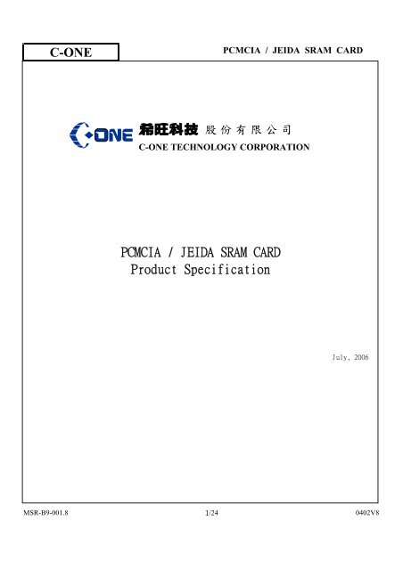
C-<strong>ONE</strong><br />
<strong>PCMCIA</strong> / <strong>JEIDA</strong> <strong>SRAM</strong> <strong>CARD</strong><br />
股 份 有 限 公 司<br />
C-<strong>ONE</strong> TECHNOLOGY CORPORATION<br />
<strong>PCMCIA</strong> / <strong>JEIDA</strong> <strong>SRAM</strong> <strong>CARD</strong><br />
<strong>Product</strong> <strong>Specification</strong><br />
July, 2006<br />
MSR-B9-001.8 1/24 0402V8
C-<strong>ONE</strong><br />
<strong>PCMCIA</strong> / <strong>JEIDA</strong> <strong>SRAM</strong> <strong>CARD</strong><br />
Contents<br />
1. FEATURES .........................................................................................................................................................................1<br />
2. GENERAL DESCRIPTION..............................................................................................................................................1<br />
3. PRODUCT NUMBER DEFINITION...............................................................................................................................2<br />
4. PRODUCT LIST........................................................................................................................... 錯 誤 ! 尚 未 定 義 書 籤 。<br />
5. PIN CONFIGURATION....................................................................................................................................................4<br />
6. PIN DESCRIPTION...........................................................................................................................................................5<br />
7. BLOCK DIAGRAM ...........................................................................................................................................................6<br />
8. RECOMMENDED OPERATING CONDITIONS........................................................................................................12<br />
9. FUNCTION TABLE.........................................................................................................................................................13<br />
10. DC ELECTRICAL CHARACTERISTICS....................................................................................................................15<br />
11. AC ELECTRICAL CHARACTERISTICS ( COMMON MEMORY ) ......................................................................16<br />
12. TIMING DIAGRAM ( COMMON MEMORY )...........................................................................................................17<br />
13. AC ELECTRICAL CHARACTERISTICS ( ATTRIBUTE MEMORY ) ..................................................................19<br />
14. TIMING DIAGRAM ( ATTRIBUTE MEMORY ).......................................................................................................20<br />
15. MAIN BATTERY SPECIFICATIONS ..........................................................................................................................21<br />
16. POWER-UP / POWER-DOWN CHARACTERISTICS...............................................................................................22<br />
17. OUTLINE DIMENSIONS (UNIT: MM)........................................................................................................................23<br />
MSR-B9-001.8 2/24 0402V8
C-<strong>ONE</strong><br />
<strong>PCMCIA</strong> / <strong>JEIDA</strong> <strong>SRAM</strong> <strong>CARD</strong><br />
Features<br />
<strong>PCMCIA</strong> / <strong>JEIDA</strong> standard<br />
256K bytes ~ 8M bytes memory capacity<br />
Byte (x8) / word (x16) data bus selectable<br />
Fast access time : 150ns (maximum)<br />
Attribute memory : 8K byte E 2 PROM or no attribute<br />
memory<br />
Single +5V operating voltage<br />
Dual back-up battery design<br />
Both BR2325 and CR2025 used as main<br />
battery<br />
Battery voltage detection function<br />
Built-in write protect switch<br />
Battery case lock system<br />
Connector type : 2-piece,2-row,68 pins<br />
Credit card size : 54.0 x 85.6 x 3.3 (mm)<br />
General Description<br />
C-<strong>ONE</strong>'s high performance <strong>SRAM</strong> cards conform to the <strong>PCMCIA</strong> / <strong>JEIDA</strong> international standard and consist of<br />
multiple very low power consumption CMOS <strong>SRAM</strong> ICs , decoder IC and power control IC mounted on a very thin<br />
printed circuit board using surface mounting technology.<br />
With the dual back-up battery design , each <strong>SRAM</strong> card contains a replaceable but non-rechargeable 3V lithium<br />
battery (main battery) and an on-board rechargeable but non-replaceable battery (auxiliary battery) for data<br />
retention. This design allows replacement of main battery without data loss for 20 minutes approximately. Digital<br />
signals on the BVD1*/BVD2* pins were used to alarm the user whether the main battery should be replaced to<br />
prevent the stored data from loss. With the flexible and user-friendly design , both BR2325 and CR2025 can be<br />
used as main battery. There is battery case lock system to prevent battery dropping from the card. Also , with the<br />
write-protect switch design , data will not be written into the card by accident.<br />
Memory card attribute information represents various attribute information of a card and is stored at EVEN address<br />
of an attribute memory space which is enabled by asserting REG* signal. Regarding to the attribute information<br />
format , please refer to the <strong>PCMCIA</strong> 2.0 or <strong>JEIDA</strong> 4.1 specification.<br />
With the flexible design of this series cards , they provide 8K bytes E 2 PROM available for attribute memory or<br />
there is no attribute memory.<br />
MSR-B9-001.8 1/24 0402V8
C-<strong>ONE</strong><br />
<strong>PCMCIA</strong> / <strong>JEIDA</strong> <strong>SRAM</strong> <strong>CARD</strong><br />
<strong>Product</strong> Number Definition<br />
X1 X2 X3 X4X5X6<br />
<strong>SRAM</strong> <strong>CARD</strong><br />
S=<strong>SRAM</strong><br />
A/M<br />
N:No A/M<br />
6:With 8KB Read/Write A/M<br />
9:With 8KB Read Only A/M<br />
Operating Voltage<br />
5=5V<br />
Memory Capacity<br />
256: 256KB<br />
512 : 512KB<br />
001 : 1MB<br />
002 : 2MB<br />
004 : 4MB<br />
006 : 6MB<br />
008 : 8MB<br />
Note : A/M means attribute memory.<br />
MSR-B9-001.8 2/24 0402V8
C-<strong>ONE</strong><br />
<strong>PCMCIA</strong> / <strong>JEIDA</strong> <strong>SRAM</strong> <strong>CARD</strong><br />
<strong>Product</strong> List<br />
Item Part Number Memory Capacity Attribute Power<br />
No. Bytes Words Memory Consumption<br />
1 S65256 256K 128K<br />
2 S65512 512K 256K<br />
3 S65001 1M 512K<br />
4 S65002 2M 1M<br />
8KB E 2 PROM Super Low<br />
5 S65004 4M 2M<br />
6 S65006 6M 3M<br />
7 SN5256 256K 128K<br />
8 SN5512 512K 256K<br />
9 SN5001 1M 512K<br />
10 SN5002 2M 1M<br />
None<br />
11 SN5004 4M 2M<br />
12 SN5006 6M 3M<br />
MSR-B9-001.8 3/24 0402V8
C-<strong>ONE</strong><br />
<strong>PCMCIA</strong> / <strong>JEIDA</strong> <strong>SRAM</strong> <strong>CARD</strong><br />
Pin Configuration<br />
17 16 15 14 13 12 11 10 9 8 7 6 5 4 3 2 1 Pin No.<br />
V<br />
C<br />
C<br />
W<br />
E<br />
*<br />
A<br />
1<br />
4<br />
A<br />
1<br />
3<br />
A<br />
8<br />
A<br />
9<br />
A<br />
1<br />
1<br />
O<br />
E<br />
*<br />
A<br />
1<br />
0<br />
D<br />
7<br />
D<br />
6<br />
D<br />
5<br />
D<br />
4<br />
D<br />
3<br />
G<br />
N<br />
D<br />
Pin Name<br />
B<br />
U<br />
S<br />
Y<br />
*<br />
34 33 32 31 30 29 28 27 26 25 24 23 22 21 20 19 18 Pin No.<br />
G<br />
N<br />
D<br />
W<br />
P<br />
D<br />
2<br />
D<br />
1<br />
D<br />
0<br />
A<br />
0<br />
A<br />
1<br />
A<br />
2<br />
A<br />
3<br />
A<br />
4<br />
A<br />
5<br />
A<br />
6<br />
A<br />
7<br />
A<br />
1<br />
2<br />
A<br />
1<br />
5<br />
A<br />
1<br />
6<br />
N<br />
C<br />
Pin Name<br />
C<br />
E<br />
1<br />
*<br />
51 50 49 48 47 46 45 44 43 42 41 40 39 38 37 36 35 Pin No.<br />
V<br />
C<br />
C<br />
A<br />
2<br />
1<br />
A<br />
2<br />
0<br />
A<br />
1<br />
9<br />
A<br />
1<br />
8<br />
A<br />
1<br />
7<br />
N<br />
C<br />
N<br />
C<br />
N<br />
C<br />
D<br />
1<br />
5<br />
D<br />
1<br />
4<br />
D<br />
1<br />
3<br />
D<br />
1<br />
2<br />
D<br />
1<br />
1<br />
G<br />
N<br />
D<br />
Pin Name<br />
C<br />
E<br />
2<br />
*<br />
C<br />
D<br />
1<br />
*<br />
68 67 66 65 64 63 62 61 60 59 58 57 56 55 54 53 52 Pin No.<br />
G<br />
N<br />
D<br />
D<br />
1<br />
0<br />
D<br />
9<br />
D<br />
8<br />
N<br />
C<br />
N<br />
C<br />
N<br />
C<br />
N<br />
C<br />
N<br />
C<br />
N<br />
C<br />
N<br />
C<br />
A<br />
2<br />
2<br />
N<br />
C<br />
Pin Name<br />
C<br />
D<br />
2<br />
*<br />
B<br />
V<br />
D<br />
1<br />
*<br />
B<br />
V<br />
D<br />
2<br />
*<br />
R<br />
E<br />
G<br />
*<br />
Table 2<br />
Note : * mean low active<br />
256KB series : A18,A19,A20,A21,A22 = NC<br />
512KB series : A19,A20,A21,A22 = NC<br />
1MB series : A20,A21,A22 = NC<br />
2MB series : A21,A22 = NC<br />
4MB series : A22 = NC<br />
S65256 ~ S65006 series : pin16 = BUSY* , pin61 = REG*<br />
SN5256 ~ SN5006 series : pin16 = NC , pin61 = NC<br />
MSR-B9-001.8 4/24 0402V8
C-<strong>ONE</strong><br />
<strong>PCMCIA</strong> / <strong>JEIDA</strong> <strong>SRAM</strong> <strong>CARD</strong><br />
Pin Description<br />
Symbol Function I/O<br />
A0 - A22 Addresses I<br />
D0 - D15 Data Inputs/Outputs I/O<br />
CE1*/CE2* Card Enable I<br />
OE* Output Enable I<br />
WE* Write Enable I<br />
REG* Attribute Memory Enable I<br />
WP Write-protect Detect O<br />
BVD1*/BVD2* Battery Voltage Detect O<br />
BUSY* Busy Output (Open drain) O<br />
CD1*/CD2* Card Detect (tied to GND internally) O<br />
VCC +5 Volt Power Supply -<br />
GND Ground -<br />
NC No Connection -<br />
Table 3<br />
MSR-B9-001.8 5/24 0402V8
C-<strong>ONE</strong><br />
<strong>PCMCIA</strong> / <strong>JEIDA</strong> <strong>SRAM</strong> <strong>CARD</strong><br />
Block Diagram<br />
(6MB series <strong>SRAM</strong> card)<br />
A0<br />
A21<br />
A22<br />
CE1*<br />
CE2*<br />
WE*<br />
OE*<br />
REG*<br />
WP<br />
Decoder<br />
Input<br />
&<br />
Buffer<br />
CEx*<br />
x=0, 2, 4, 6<br />
CEy*<br />
y=1, 3, 5, 7<br />
Common memory<br />
1MB <strong>SRAM</strong> x4<br />
WE*<br />
OE*<br />
A0-A19<br />
Common memory<br />
1MB <strong>SRAM</strong> x4<br />
WE*<br />
OE*<br />
A0-A19<br />
D0-D7<br />
D8-D15<br />
D0-D7<br />
Data Bus<br />
Buffer<br />
D8-D15<br />
Write protect switch<br />
A1-A20<br />
VCC<br />
BVD1*<br />
BVD2*<br />
Power controller<br />
&<br />
Voltage detector<br />
Optional Attribute memory<br />
CE*<br />
WE* 2KB EEPROM<br />
OE*<br />
BUSY*<br />
A0-A10<br />
D0-D7<br />
main<br />
battery<br />
auxiliary<br />
battery<br />
D8-D15<br />
D0-D7<br />
BUSY*<br />
Note : A0,A21,A22 are chip decoding address pins.<br />
Figure 1<br />
MSR-B9-001.8 6/24 0402V8
C-<strong>ONE</strong><br />
<strong>PCMCIA</strong> / <strong>JEIDA</strong> <strong>SRAM</strong> <strong>CARD</strong><br />
Block Diagram<br />
(4MB series <strong>SRAM</strong> card)<br />
A0<br />
A20<br />
A21<br />
CE1*<br />
CE2*<br />
WE*<br />
OE*<br />
REG*<br />
WP<br />
Decoder<br />
Input<br />
&<br />
Buffer<br />
CEx*<br />
x=0, 2, 4, 6<br />
CEy*<br />
y=1, 3, 5, 7<br />
Common memory<br />
512KB <strong>SRAM</strong> x4<br />
WE*<br />
OE*<br />
A0-A18<br />
Common memory<br />
512KB <strong>SRAM</strong> x4<br />
WE*<br />
OE*<br />
A0-A18<br />
D0-D7<br />
D8-D15<br />
D0-D7<br />
Data Bus<br />
Buffer<br />
D8-D15<br />
Write protect switch<br />
A1-A19<br />
VCC<br />
BVD1*<br />
BVD2*<br />
Power controller<br />
&<br />
Voltage detector<br />
Optional Attribute memory<br />
CE*<br />
WE* 2KB EEPROM<br />
OE*<br />
BUSY*<br />
A0-A10<br />
D0-D7<br />
main<br />
battery<br />
auxiliary<br />
battery<br />
D8-D15<br />
D0-D7<br />
BUSY*<br />
Note : A0,A20,A21 are chip decoding address pins.<br />
Figure 2<br />
MSR-B9-001.8 7/24 0402V8
C-<strong>ONE</strong><br />
<strong>PCMCIA</strong> / <strong>JEIDA</strong> <strong>SRAM</strong> <strong>CARD</strong><br />
Block Diagram<br />
(2MB series <strong>SRAM</strong> card)<br />
A0<br />
A20<br />
CE1*<br />
CE2*<br />
WE*<br />
OE*<br />
REG*<br />
WP<br />
Decoder<br />
Input<br />
&<br />
Buffer<br />
CEx*<br />
x=0, 2<br />
CEy*<br />
y=1, 3<br />
Common memory<br />
512KB <strong>SRAM</strong> x2<br />
WE*<br />
OE*<br />
A0-A18<br />
Common memory<br />
512KB <strong>SRAM</strong> x2<br />
WE*<br />
OE*<br />
A0-A18<br />
D0-D7<br />
D8-D15<br />
D0-D7<br />
Data Bus<br />
Buffer<br />
D8-D15<br />
Write protect switch<br />
A1-A19<br />
VCC<br />
BVD1*<br />
BVD2*<br />
Power controller<br />
&<br />
Voltage detector<br />
Optional Attribute memory<br />
CE*<br />
WE* 2KB EEPROM<br />
OE*<br />
BUSY*<br />
A0-A10<br />
D0-D7<br />
main<br />
battery<br />
auxiliary<br />
battery<br />
D8-D15<br />
D0-D7<br />
BUSY*<br />
Note : A0,A20 are chip decoding address pins.<br />
Figure 3<br />
MSR-B9-001.8 8/24 0402V8
C-<strong>ONE</strong><br />
<strong>PCMCIA</strong> / <strong>JEIDA</strong> <strong>SRAM</strong> <strong>CARD</strong><br />
Block Diagram<br />
(1MB series <strong>SRAM</strong> card)<br />
A0<br />
CE1*<br />
CE2*<br />
WE*<br />
OE*<br />
REG*<br />
WP<br />
Decoder<br />
Input<br />
&<br />
Buffer<br />
CEx*<br />
x=0,<br />
CEy*<br />
y=1,<br />
Common memory<br />
512KB <strong>SRAM</strong> x1<br />
WE*<br />
OE*<br />
A0-A18<br />
Common memory<br />
512KB <strong>SRAM</strong> x1<br />
WE*<br />
OE*<br />
A0-A18<br />
D0-D7<br />
D8-D15<br />
D0-D7<br />
Data Bus<br />
Buffer<br />
D8-D15<br />
Write protect switch<br />
A1-A19<br />
VCC<br />
BVD1*<br />
BVD2*<br />
Power controller<br />
&<br />
Voltage detector<br />
Optional Attribute memory<br />
CE*<br />
WE* 2KB EEPROM<br />
OE*<br />
BUSY*<br />
A0-A10<br />
D0-D7<br />
main<br />
battery<br />
auxiliary<br />
battery<br />
D8-D15<br />
D0-D7<br />
BUSY*<br />
Note : A0 is chip decoding address pin.<br />
Figure 4<br />
MSR-B9-001.8 9/24 0402V8
C-<strong>ONE</strong><br />
<strong>PCMCIA</strong> / <strong>JEIDA</strong> <strong>SRAM</strong> <strong>CARD</strong><br />
Block Diagram<br />
(512KB series <strong>SRAM</strong> card)<br />
A0<br />
A18<br />
CE1*<br />
CE2*<br />
WE*<br />
OE*<br />
REG*<br />
WP<br />
Decoder<br />
Input<br />
&<br />
Buffer<br />
CEx*<br />
x=0, 2<br />
CEy*<br />
y=1, 3<br />
Common memory<br />
128KB <strong>SRAM</strong> x2<br />
WE*<br />
OE*<br />
A0-A16<br />
D0-D7<br />
Common memory<br />
128KB <strong>SRAM</strong> x2<br />
D8-D15<br />
WE*<br />
OE*<br />
A0-A16<br />
D0-D7<br />
Data Bus<br />
Buffer<br />
D8-D15<br />
Write protect switch<br />
A1-A17<br />
VCC<br />
BVD1*<br />
BVD2*<br />
Power controller<br />
&<br />
Voltage detector<br />
Optional Attribute memory<br />
CE*<br />
WE* 2KB EEPROM<br />
OE*<br />
BUSY*<br />
A0-A10<br />
D0-D7<br />
main<br />
battery<br />
auxiliary<br />
battery<br />
D8-D15<br />
D0-D7<br />
BUSY*<br />
Note : A0,A18 are chip decoding address pins.<br />
Figure 5<br />
MSR-B9-001.8 10/24 0402V8
C-<strong>ONE</strong><br />
<strong>PCMCIA</strong> / <strong>JEIDA</strong> <strong>SRAM</strong> <strong>CARD</strong><br />
Block Diagram<br />
(256KB series <strong>SRAM</strong> card)<br />
A0<br />
CE1*<br />
CE2*<br />
WE*<br />
OE*<br />
REG*<br />
WP<br />
Decoder<br />
Input<br />
&<br />
Buffer<br />
CEx*<br />
x=0<br />
CEy*<br />
y=1<br />
Common memory<br />
128KB <strong>SRAM</strong> x1<br />
WE*<br />
OE*<br />
A0-A16<br />
Common memory<br />
128KB <strong>SRAM</strong> x1<br />
WE*<br />
OE*<br />
A0-A16<br />
D0-D7<br />
D8-D15<br />
D0-D7<br />
Data Bus<br />
Buffer<br />
D8-D15<br />
Write protect switch<br />
A1-A17<br />
VCC<br />
BVD1*<br />
BVD2*<br />
Power controller<br />
&<br />
Voltage detector<br />
Optional Attribute memory<br />
CE*<br />
WE* 2KB EEPROM<br />
OE*<br />
BUSY*<br />
A0-A10<br />
D0-D7<br />
main<br />
battery<br />
auxiliary<br />
battery<br />
D8-D15<br />
D0-D7<br />
BUSY*<br />
Note : A0 is chip decoding address pin.<br />
Figure 6<br />
MSR-B9-001.8 11/24 0402V8
C-<strong>ONE</strong><br />
<strong>PCMCIA</strong> / <strong>JEIDA</strong> <strong>SRAM</strong> <strong>CARD</strong><br />
Pin Location<br />
Recommended Operating Conditions<br />
Figure 9 Bottom View (Connector Side)<br />
Parameter Symbol Min. Max. Unit<br />
Supply Voltage V CC 4.5 5.5 V<br />
Input High Voltage V IH 0.7VCC VCC + 0.3 V<br />
Input Low Voltage V IL - 0.3 0.8 V<br />
Battery Voltage V BAT 2.37 V<br />
Operating Temperature ( Commercial ) T OPR 0 60 ℃<br />
Operating Temperature ( Industrial ) T OPR -40 85 ℃<br />
Relative Humidity (non-condensing) H UM 95 %<br />
Absolute Maximum Ratings *<br />
Table 4<br />
*Comments<br />
Parameter Symbol Value Unit<br />
Supply Voltage V CC -0.5 to + 6.0 V<br />
Input Voltage V IN -0.5 to V CC + 0.3 (6V max.) V<br />
Output Voltage V OUT -0.5 to + 6.0 V<br />
Operating Temperature ( Commercial ) T OPR -10 to + 70 ℃<br />
Storage Temperature ( Commercial ) T STR -20 to + 70 ℃<br />
Operating Temperature ( Industrial ) T OPR -40 to + 85 ℃<br />
Storage Temperature( Industrial ) T STR -40 to + 85 ℃<br />
Relative Humidity (non-condensing) H UM 95 (maximum) %<br />
Table 5<br />
Stress above those listed under " Absolute Maximum Ratings " may cause permanent damage to the products. These<br />
are stress rating only. Functional operation of these products at these or any other conditions above those indicated<br />
in the operational sections of this specification is not implied. Exposure to absolute maximum rating conditions for<br />
extended periods may affect product reliability.<br />
MSR-B9-001.8 12/24 0402V8
C-<strong>ONE</strong><br />
<strong>PCMCIA</strong> / <strong>JEIDA</strong> <strong>SRAM</strong> <strong>CARD</strong><br />
Function Table<br />
( Write is NOT protected )<br />
Function REG* CE2* CE1* A0 OE* WE* WP D15 - D8 D7 - D0<br />
Read C/M (x8) H H L L L H L High - Z Even Byte Data Out<br />
Read C/M (x8) H H L H L H L High - Z Odd Byte Data Out<br />
Read C/M (x8) H L H X L H L Odd Byte Data Out High - Z<br />
Read C/M (x16) H L L X L H L Odd Byte Data Out Even Byte Data Out<br />
Write C/M (x8) H H L L H L L X Even Byte Data In<br />
Write C/M (x8) H H L H H L L X Odd Byte Data In<br />
Write C/M (x8) H L H X H L L Odd Byte Data In X<br />
Write C/M (x16) H L L X H L L Odd Byte Data In Even Byte Data In<br />
Standby X H H X X X L High - Z High - Z<br />
Output Disable X X X X H H L High - Z High - Z<br />
Read A/M (x8) L H L L L H L High - Z Even Byte Data Out<br />
Read A/M (x8) L H L H L H L High - Z Data Out (invalid)<br />
Read A/M (x8) L L H X L H L Data Out (invalid) High - Z<br />
Read A/M (x16) L L L X L H L Data Out (invalid) Even Byte Data Out<br />
Write A/M (x8) L H L L H L L X Even Byte Data In<br />
Write A/M (x8) L H L H H L L X X<br />
Write A/M (x8) L L H X H L L X X<br />
Write A/M (x16) L L L X H L L X Even Byte Data In<br />
Table 6<br />
Function Table<br />
( Write is protected )<br />
Function REG* CE2* CE1* A0 OE* WE* WP D15 - D8 D7 - D0<br />
Read C/M (x8) H H L L L H H High - Z Even Byte Data Out<br />
Read C/M (x8) H H L H L H H High - Z Odd Byte Data Out<br />
Read C/M (x8) H L H X L H H Odd Byte Data Out High - Z<br />
Read C/M (x16) H L L X L H H Odd Byte Data Out Even Byte Data Out<br />
Write C/M (x8) H H L L H L H X X<br />
Write C/M (x8) H H L H H L H X X<br />
Write C/M (x8) H L H X H L H X X<br />
Write C/M (x16) H L L X H L H X X<br />
Standby X H H X X X H High - Z High - Z<br />
Output Disable X X X X H H H High - Z High - Z<br />
Read A/M (x8) L H L L L H H High - Z Even Byte Data Out<br />
Read A/M (x8) L H L H L H H High - Z Data Out (invalid)<br />
Read A/M (x8) L L H X L H H Data Out (invalid) High - Z<br />
Read A/M (x16) L L L X L H H Data Out (invalid) Even Byte Data Out<br />
Write A/M (x8) L H L L H L H X X<br />
Write A/M (x8) L H L H H L H X X<br />
Write A/M (x8) L L H X H L H X X<br />
Write A/M (x16) L L L X H L H X X<br />
Table 7<br />
Definition : C/M = Common Memory, A/M = Attribute Memory<br />
L = V IL ; H = V IH ; X = don't care can be either V IH or V IL<br />
MSR-B9-001.8 13/24 0402V8
C-<strong>ONE</strong><br />
<strong>PCMCIA</strong> / <strong>JEIDA</strong> <strong>SRAM</strong> <strong>CARD</strong><br />
Common Memory Address Configuration Using 8-bit Data Bus (CE2*=VIH,CE1*=VIL)<br />
A22 to A0 D15 -- D8 D7 -- D0<br />
00 0000 0000 0000 0000 0000 High - Z Address 0<br />
00 0000 0000 0000 0000 0001 High - Z Address 1<br />
00 0000 0000 0000 0000 0010 High - Z Address 2<br />
↓ ↓ ↓<br />
11 1111 1111 1111 1111 1101 High - Z Address 8388605<br />
11 1111 1111 1111 1111 1110 High - Z Address 8388606<br />
11 1111 1111 1111 1111 1111 High - Z Address 8388607<br />
Table 8<br />
Common Memory Address Configuration Using 8-bit Data Bus (CE2*=VIL,CE1*=VIH)<br />
A22 to A0 D15 -- D8 D7 -- D0<br />
00 0000 0000 0000 0000 000X Address 1 High - Z<br />
00 0000 0000 0000 0000 001X Address 3 High - Z<br />
00 0000 0000 0000 0000 010X Address 5 High - Z<br />
↓ ↓ ↓<br />
11 1111 1111 1111 1111 101X Address 8388603 High - Z<br />
11 1111 1111 1111 1111 110X Address 8388605 High - Z<br />
11 1111 1111 1111 1111 111X Address 8388607 High - Z<br />
Table 9<br />
Common Memory Address Configuration Using 16-bit Data Bus (CE2*=VIL,CE1*=VIL)<br />
A22 to A0 D15 -- D8 D7 -- D0<br />
00 0000 0000 0000 0000 000X Address 1 Address 0<br />
00 0000 0000 0000 0000 001X Address 3 Address 2<br />
00 0000 0000 0000 0000 010X Address 5 Address 4<br />
↓ ↓ ↓<br />
11 1111 1111 1111 1111 101X Address 8388603 Address 8388602<br />
11 1111 1111 1111 1111 110X Address 8388605 Address 8388604<br />
11 1111 1111 1111 1111 111X Address 8388607 Address 8388606<br />
Table 10<br />
The above tables are examples for 8M bytes /4M words <strong>SRAM</strong> cards.<br />
Definition : L = VIL; H = VIH; X = don't care , can be either VIH or VIL.<br />
MSR-B9-001.8 14/24 0402V8
C-<strong>ONE</strong><br />
<strong>PCMCIA</strong> / <strong>JEIDA</strong> <strong>SRAM</strong> <strong>CARD</strong><br />
DC Electrical Characteristics<br />
(recommended operating conditions unless otherwise noted)<br />
Symbol Parameter Min. Max. Unit Test Conditions<br />
I LI Input Leakage Current -10 10 uA V IN = 0V to Vcc ( Note 3 )<br />
-70 10 uA V IN = 0V to Vcc ( Note 4 )<br />
I LO Output Leakage Current -10 10 uA CE1* = CE2* = V IH or OE* = V IH ,<br />
V I/O = 0V to V CC ( Note 1 )<br />
V OH Output High Voltage 3.8 V I OH = -2mA (Note 2)<br />
V OL Output Low Voltage 0.4 V I OL = 3.2mA ( Note 2 )<br />
V IH Input High Voltage 0.7Vcc Vcc+0.3 V<br />
V IL Input Low Voltage -0.3 0.3Vcc V<br />
I CC Vcc Operating Current 120 mA Min. cycle , I Out = 0mA<br />
I SB Vcc Standby Current 0.1 mA For page 3 & 4, item 9<br />
( CE1*= CE2*= V IH or 0.2 mA For page 3 & 4, item 10<br />
CE1*= CE2*≥VCC - 0.2V ) 0.1 mA For page 3 & 4, item 11<br />
0.2 mA For page 3 & 4, item 12<br />
0.1 mA For page 3 & 4, item 13<br />
0.2 mA For page 3 & 4, item 14<br />
0.3 mA For page 3 & 4, item 15<br />
0.3 mA For page 3 & 4, item 16<br />
0.15 mA For page 3 & 4, item 1<br />
0.25 mA For page 3 & 4, item 2<br />
0.15 mA For page 3 & 4, item 3<br />
0.25 mA For page 3 & 4, item 4<br />
0.15 mA For page 3 & 4, item 5<br />
0.25 mA For page 3 & 4, item 6<br />
0.35 mA For page 3 & 4, item 7<br />
0.35 mA For page 3 & 4, item 8<br />
I BU Battery Back-up Current 256KB 40 uA 1uA (Ta = 25℃)<br />
(All pins open , V BAT = 3V 512KB 80 uA 2uA (Ta = 25℃)<br />
V CC = 0V) 1MB 50 uA 1uA (Ta = 25℃)<br />
2MB 100 uA 2uA (Ta = 25℃)<br />
4MB 200 uA 4uA (Ta = 25℃)<br />
6MB 160 uA 4uA (Ta = 25℃)<br />
V BDET1 Battery Detect Reference Voltage 1 2.27 2.47 V 2.37V (Typ.) Vcc = 5V , Ta = 25℃<br />
V BDET2 Battery Detect Reference Voltage 2 2.55 2.75 V 2.65V (Typ.) Vcc = 5V , Ta = 25℃<br />
Table 11<br />
Note: 1.) Except BVD1*,BVD2*,CD1*,CD2* pins.<br />
2.) Except CD1*,CD2* pins.<br />
3.) Except CE1*,CE2*,WE*,REG* pins.<br />
4.) For CE1*,CE2*,WE*,REG* pins.<br />
MSR-B9-001.8 15/24 0402V8
C-<strong>ONE</strong><br />
<strong>PCMCIA</strong> / <strong>JEIDA</strong> <strong>SRAM</strong> <strong>CARD</strong><br />
AC Electrical Characteristics ( Common Memory )<br />
( recommended operating conditions unless otherwise noted )<br />
Read Cycle ( Common Memory )<br />
Symbol Parameter Min. Max. Unit Test Condition<br />
t cr Read Cycle Time 150 ns<br />
t a(A) Address Access Time 150 ns<br />
t a(CE) Card Enable Access Time 150 ns<br />
t a(OE) Output Enable Access Time 75 ns<br />
t dis(CE) Output Disable Time (CE*) 75 ns<br />
t dis(OE) Output Disable Time (OE*) 75 ns<br />
t en(CE) Output Enable Time (CE*) 5 ns<br />
t en(OE) Output Enable Time (OE*) 5 ns<br />
t v(A) Data Hold Time (from address changed) 0 ns<br />
Table 12<br />
Write Cycle ( Common Memory )<br />
Symbol Parameter Min. Max Unit Test Condition<br />
t cw Write Cycle Time 150 ns<br />
t w(WE) Write Pulse Width 80 ns<br />
tsu(A) Address Setup Time 20 ns<br />
t su(A-WEH) Address Setup Time (WE*) 100 ns<br />
t su(CE-WEH) CE* Setup Time (WE*) 100 ns<br />
t su(D-WEH) Data Setup Time (WE*) 50 ns<br />
t h(D) Data Hold Time 20 ns<br />
t rec(WE) Write Recovery Time 20 ns<br />
t dis(WE) Output Disable Time (WE*) 75 ns<br />
t dis(OE) Output Disable Time (OE*) 75 ns<br />
t en(WE) Output Enable Time (WE*) 5 ns<br />
t en(OE) Output Enable Time (OE*) 5 ns<br />
t en(OE-WE) Output Enable Setup Time (WE*) 10 ns<br />
t h(OE-WE) Output Enable Hold Time (WE*) 10 ns<br />
Table 13<br />
MSR-B9-001.8 16/24 0402V8
C-<strong>ONE</strong><br />
<strong>PCMCIA</strong> / <strong>JEIDA</strong> <strong>SRAM</strong> <strong>CARD</strong><br />
AC Characteristics Test Conditions<br />
Input Pulse Level V OH = 0.7Vcc , V IL = 0.8V<br />
Input Rise and Fall Time<br />
5ns (max)<br />
Timing Measurement Reference V IH / V IL = 2.4V / 0.6V , V OH / V OL = 2V / 0.8V<br />
Level<br />
Output Load 1TTL Gate + 100PF (Figure 9)<br />
Table 14<br />
Figure 10 :<br />
Dout<br />
+5V<br />
1.8K OHM<br />
990 OHM<br />
100PF*<br />
*: Including scope and jig<br />
Input / Output Capacitance<br />
(Ta = 25 蚓 , f = 1MHZ,Vin/Vout = 0V) , these parameters are sampled not 100% tested.<br />
Symbol Parameter Min. Max. Unit<br />
Cin Input Capacitance 110 PF<br />
Ci/o I/O Capacitance 35 PF<br />
Table 15<br />
Timing Diagram ( Common Memory )<br />
Read Cycle Timing Diagram ( Common Memory ) ( WE*=REG*=VIH )<br />
Address<br />
(A0-An)<br />
t<br />
a(A)<br />
t cr<br />
t<br />
v(A)<br />
CE1* or/and<br />
CE2*<br />
t<br />
a(CE)<br />
t<br />
dis(CE)<br />
OE*<br />
t<br />
a(OE)<br />
Data Out<br />
High-Z<br />
t<br />
t<br />
en(CE)<br />
en(OE)<br />
DATA<br />
VALID<br />
t<br />
dis(OE)<br />
Figure 11<br />
Note : 1) For 64KB , An = A15. 128KB , An = A16. 256KB , An = A17. 512KB , An = A18.<br />
1MB , An = A19. 2MB , An = A20. 4MB , An = A21 6MB , An = A22.<br />
2) The shaded area may be either high or low.<br />
MSR-B9-001.8 17/24 0402V8
C-<strong>ONE</strong><br />
<strong>PCMCIA</strong> / <strong>JEIDA</strong> <strong>SRAM</strong> <strong>CARD</strong><br />
Write Cycle Timing Diagram ( Common Memory ) ( REG*=VIH , WE* controlled )<br />
Address<br />
(A0-An)<br />
CE1* or/and<br />
CE2*<br />
t<br />
t<br />
su(A-WEH)<br />
t CW<br />
su(CE-WEH)<br />
OE*<br />
WE*<br />
High-Z<br />
Data In<br />
Data Out<br />
t<br />
su(A)<br />
t dis<br />
(OE)<br />
t<br />
su(OE-WE)<br />
tdis<br />
t<br />
w(WE)<br />
t<br />
su(D-WEH)<br />
t rec<br />
DATA INPUT VALID<br />
(WE)<br />
High-Z<br />
Figure 12<br />
t en<br />
(OE)<br />
(WE)<br />
th<br />
(OE-WE)<br />
t h<br />
t<br />
(D)<br />
en(WE)<br />
Write Cycle Timing Diagram ( Common Memory ) ( CE* controlled , OE*=REG*=Vih)<br />
Address<br />
(A0-An)<br />
CE1* or/and<br />
CE2*<br />
WE*<br />
t<br />
su(A)<br />
t su<br />
t CW<br />
(CE-WEH)<br />
t rec<br />
(WE)<br />
Data In<br />
High-Z<br />
t su<br />
(D-WEH)<br />
DATA INPUT VALID<br />
t h<br />
(D)<br />
Figure 13<br />
Note : 1) For 64KB , An = A15. 128KB , An = A16. 256KB , An = A17. 512KB , An = A18.<br />
1MB , An = A19. 2MB , An = A20. 4MB , An = A21 6MB , An = A22.<br />
2) The shaded area may be either high or low.<br />
MSR-B9-001.8 18/24 0402V8
C-<strong>ONE</strong><br />
<strong>PCMCIA</strong> / <strong>JEIDA</strong> <strong>SRAM</strong> <strong>CARD</strong><br />
AC Electrical Characteristics ( Attribute Memory )<br />
( recommended operating conditions unless otherwise noted )<br />
Read Cycle ( Attribute Memory )<br />
Symbol Parameter Min. Max Unit Test Condition<br />
t cr Read Cycle Time 300 ns<br />
t a(A) Address Access Time 300 ns<br />
t a(CE) Card Select Access Time 300 ns<br />
t a(OE) Output Enable Access Time 150 ns<br />
t dis(CE) Output Disable Time (from CE*) 100 ns<br />
t dis(OE) Output Disable Time (from OE*) 100 ns<br />
t en(CE) Output Enable Time (from CE*) 5 ns<br />
t en(OE) Output Enable Time (from OE*) 5 ns<br />
t v(A) Data Hold Time (from address changed) 0 ns<br />
Table 16<br />
Write Cycle ( Attribute Memory )<br />
Symbol Parameter Min. Max. Unit Test Condition<br />
t CW Write Cycle Time 1 ms<br />
t AS Address Setup Time 30 ns<br />
t AH Address Hold Time 50 ns<br />
t WP Write Pulse Width 120 ns<br />
t CS Card Enable Time to WE* 15 ns<br />
t CH Card Enable Hold Time from WE* High 0 ns<br />
t DS Data Setup Time 70 ns<br />
t DH Data Hold Time 30 ns<br />
t OES OE* Setup Time 30 ns<br />
t OEH OE* Hold Time 30 ns<br />
t DB Delay from WE* high to BUSY* Asserted 50 ns<br />
Table 17<br />
MSR-B9-001.8 19/24 0402V8
C-<strong>ONE</strong><br />
<strong>PCMCIA</strong> / <strong>JEIDA</strong> <strong>SRAM</strong> <strong>CARD</strong><br />
Timing Diagram ( Attribute Memory )<br />
Read Cycle Timing Diagram ( Attribute Memory ) ( REG*=VIL , WE*=VIH )<br />
Address<br />
(A1-A11)<br />
t<br />
a(A)<br />
t cr<br />
t<br />
v(A)<br />
CE1* or/and<br />
CE2*<br />
t<br />
a(CE)<br />
t<br />
dis(CE)<br />
OE*<br />
Data Out<br />
t<br />
t<br />
en(CE)<br />
t<br />
en(OE)<br />
a(OE)<br />
DATA<br />
VALID<br />
t<br />
dis(OE)<br />
Figure 14<br />
Write Cycle Timing Diagram ( Attribute Memory ) ( REG*=VIL )<br />
Address<br />
(A1-A11)<br />
t AH<br />
CE1* or/and<br />
CE2*<br />
t CS<br />
t CH<br />
WE*<br />
t AS<br />
tWP<br />
OE*<br />
t OES<br />
t<br />
t OEH<br />
h(D)<br />
t DS<br />
Data In<br />
DATA INPUT VALID<br />
RDY/BUSY*<br />
t DB<br />
Figure 15<br />
t CW<br />
MSR-B9-001.8 20/24 0402V8
C-<strong>ONE</strong><br />
<strong>PCMCIA</strong> / <strong>JEIDA</strong> <strong>SRAM</strong> <strong>CARD</strong><br />
Battery Voltage Detection<br />
BVD1*/BVD2* pins are used to monitor the voltage of the main battery which should be maintained at 2.65V or<br />
greater for data retention. The following table described the main battery status by reading the signals on<br />
BVD1*/BVD2* pins.<br />
BVD1* BVD2* Main Battery Comments<br />
H H V BAT ≥ 2.65V Data retention is OK. Battery is operational<br />
H L 2.37V < V BAT < 2.65V Data retention is OK. But battery should be replaced.<br />
L L V BAT < 2.37V Data integrity is not guaranteed.<br />
Battery must be replaced.<br />
Table 18<br />
Note : if the main battery is removed , BVD1* and BVD2* pins will not function<br />
Main Battery <strong>Specification</strong>s<br />
• 3V Lithium battery<br />
• Recommended parts (Please refer to the table below)<br />
Diameter Thickness Brand Model No. Diameter Thickness Brand Model No.<br />
23.0mm 2.5mm RAYOVAC BR2325 20.0mm 2.5mm TOSHIBA CR2025<br />
FDK CR2325 FDK CR2025<br />
PANASONIC BR2325 PANASONIC CR2025<br />
Approximate Battery Life Time Under Battery Back-up Only<br />
( Ta=25°C, Humidity=60% R.H. ) *battery life unit : year<br />
<strong>Product</strong> Part No. Battery Life <strong>Product</strong> Part No. Battery Life<br />
SA5256 6 / 4.5 SN5256 6 / 4.5<br />
SA5512 4 / 3 SN5512 4 / 3<br />
SA5001 6 / 4.5 SN5001 6 / 4.5<br />
SA5002 4 / 3 SN5002 4 / 3<br />
SA5004 2.5 / 2 SN5004 2.5 / 2<br />
SA5006 2.5 / 2 SN5006 2.5 / 2<br />
Table 19<br />
*For battery life , the numbers on the left-hand side of slash denote using 2325 series batteries. The numbers on<br />
the right-hand side of slash denote using 2025 series batteries.<br />
Card Detection<br />
CD1* , CD2* pins are used to detect the insertion of the card into the system. When the memory card has been<br />
correctly inserted , CD1* and CD2* are detected by the system . The recommended circuit in the system side is<br />
shown in figure below.<br />
VCC<br />
(A)<br />
VCC<br />
CD1*<br />
(B)<br />
Figure 16<br />
CD2*<br />
MSR-B9-001.8 21/24 0402V8
C-<strong>ONE</strong><br />
<strong>PCMCIA</strong> / <strong>JEIDA</strong> <strong>SRAM</strong> <strong>CARD</strong><br />
Power-up / Power-down Characteristics<br />
Symbol Parameter Min. Max. Unit Condition Note<br />
Vi(CE) CE * Signal Level 0 ViMAX V 0V ≤ VCC < 2.0 1<br />
VCC-0.1 ViMAX V 2.0 ≤ VCC < V IH<br />
V IH ViMAX V V IH ≤ VCC<br />
t su(VCC) CE * Setup Time 20 ms 10ms (Typ.)<br />
t rec(VCC) CE * Recovery Time 1 us<br />
t pr VCC Rising Time 0.1 300 ms 10% → 90% (VCC+5%) 1<br />
t pf VCC Falling Time 3.0 300 ms 90% (VCC-5%) → 10% 1<br />
Table20<br />
Note:<br />
1.) ViMAX means absolute maximum voltage for input.<br />
2.) For the period 0V ≤ VCC< 2.0V , power supply voltage is low , so 0V~ ViMAX is permitted , because the<br />
logic for the system interface IC may not be determined.<br />
3.) The Tpr and Tpfare defined as " linear waveform " in the period of 10% to 90%. Even if the waveform is<br />
not " linear waveform " , its rising and falling time must meet this specification.<br />
Power-up Timing Diagram<br />
t pr<br />
VCC<br />
t SU(VCC)<br />
V ih<br />
2V<br />
CE1*,CE2*<br />
Figure 17<br />
Power-down Timing Diagram<br />
VCC<br />
t pf<br />
t rec(VCC)<br />
V ih<br />
CE1*,CE2*<br />
2V<br />
MSR-B9-001.8 22/24 0402V8
C-<strong>ONE</strong><br />
<strong>PCMCIA</strong> / <strong>JEIDA</strong> <strong>SRAM</strong> <strong>CARD</strong><br />
Figure 18<br />
Outline Dimensions (Unit: mm)<br />
MSR-B9-001.8 23/24 0402V8