PIC24HJ64 Datasheet
PIC24HJ64 Datasheet
PIC24HJ64 Datasheet

You also want an ePaper? Increase the reach of your titles
YUMPU automatically turns print PDFs into web optimized ePapers that Google loves.
PIC24HJ32GP302/304,<br />
<strong>PIC24HJ64</strong>GPX02/X04, and<br />
PIC24HJ128GPX02/X04<br />
Data Sheet<br />
High-Performance, 16-bit<br />
Microcontrollers<br />
© 2008 Microchip Technology Inc. Preliminary DS70293B
Note the following details of the code protection feature on Microchip devices:<br />
• Microchip products meet the specification contained in their particular Microchip Data Sheet.<br />
• Microchip believes that its family of products is one of the most secure families of its kind on the market today, when used in the<br />
intended manner and under normal conditions.<br />
• There are dishonest and possibly illegal methods used to breach the code protection feature. All of these methods, to our<br />
knowledge, require using the Microchip products in a manner outside the operating specifications contained in Microchip’s Data<br />
Sheets. Most likely, the person doing so is engaged in theft of intellectual property.<br />
• Microchip is willing to work with the customer who is concerned about the integrity of their code.<br />
• Neither Microchip nor any other semiconductor manufacturer can guarantee the security of their code. Code protection does not<br />
mean that we are guaranteeing the product as “unbreakable.”<br />
Code protection is constantly evolving. We at Microchip are committed to continuously improving the code protection features of our<br />
products. Attempts to break Microchip’s code protection feature may be a violation of the Digital Millennium Copyright Act. If such acts<br />
allow unauthorized access to your software or other copyrighted work, you may have a right to sue for relief under that Act.<br />
Information contained in this publication regarding device<br />
applications and the like is provided only for your convenience<br />
and may be superseded by updates. It is your responsibility to<br />
ensure that your application meets with your specifications.<br />
MICROCHIP MAKES NO REPRESENTATIONS OR<br />
WARRANTIES OF ANY KIND WHETHER EXPRESS OR<br />
IMPLIED, WRITTEN OR ORAL, STATUTORY OR<br />
OTHERWISE, RELATED TO THE INFORMATION,<br />
INCLUDING BUT NOT LIMITED TO ITS CONDITION,<br />
QUALITY, PERFORMANCE, MERCHANTABILITY OR<br />
FITNESS FOR PURPOSE. Microchip disclaims all liability<br />
arising from this information and its use. Use of Microchip<br />
devices in life support and/or safety applications is entirely at<br />
the buyer’s risk, and the buyer agrees to defend, indemnify and<br />
hold harmless Microchip from any and all damages, claims,<br />
suits, or expenses resulting from such use. No licenses are<br />
conveyed, implicitly or otherwise, under any Microchip<br />
intellectual property rights.<br />
Trademarks<br />
The Microchip name and logo, the Microchip logo, Accuron,<br />
dsPIC, KEELOQ, KEELOQ logo, MPLAB, PIC, PICmicro,<br />
PICSTART, PRO MATE, rfPIC and SmartShunt are registered<br />
trademarks of Microchip Technology Incorporated in the<br />
U.S.A. and other countries.<br />
FilterLab, Linear Active Thermistor, MXDEV, MXLAB,<br />
SEEVAL, SmartSensor and The Embedded Control Solutions<br />
Company are registered trademarks of Microchip Technology<br />
Incorporated in the U.S.A.<br />
Analog-for-the-Digital Age, Application Maestro, CodeGuard,<br />
dsPICDEM, dsPICDEM.net, dsPICworks, dsSPEAK, ECAN,<br />
ECONOMONITOR, FanSense, In-Circuit Serial<br />
Programming, ICSP, ICEPIC, Mindi, MiWi, MPASM, MPLAB<br />
Certified logo, MPLIB, MPLINK, mTouch, PICkit, PICDEM,<br />
PICDEM.net, PICtail, PIC 32 logo, PowerCal, PowerInfo,<br />
PowerMate, PowerTool, REAL ICE, rfLAB, Select Mode, Total<br />
Endurance, UNI/O, WiperLock and ZENA are trademarks of<br />
Microchip Technology Incorporated in the U.S.A. and other<br />
countries.<br />
SQTP is a service mark of Microchip Technology Incorporated<br />
in the U.S.A.<br />
All other trademarks mentioned herein are property of their<br />
respective companies.<br />
© 2008, Microchip Technology Incorporated, Printed in the<br />
U.S.A., All Rights Reserved.<br />
Printed on recycled paper.<br />
Microchip received ISO/TS-16949:2002 certification for its worldwide<br />
headquarters, design and wafer fabrication facilities in Chandler and<br />
Tempe, Arizona; Gresham, Oregon and design centers in California<br />
and India. The Company’s quality system processes and procedures<br />
are for its PIC ® MCUs and dsPIC ® DSCs, KEELOQ ® code hopping<br />
devices, Serial EEPROMs, microperipherals, nonvolatile memory and<br />
analog products. In addition, Microchip’s quality system for the design<br />
and manufacture of development systems is ISO 9001:2000 certified.<br />
DS70293B-page ii Preliminary © 2008 Microchip Technology Inc.
PIC24HJ32GP302/304,<br />
<strong>PIC24HJ64</strong>GPX02/X04, AND<br />
PIC24HJ128GPX02/X04<br />
High-Performance, 16-bit Microcontrollers<br />
Operating Range:<br />
• Up to 40 MIPS operation (at 3.0-3.6V):<br />
- Industrial temperature range<br />
(-40°C to +85°C)<br />
- Extended temperature range<br />
(-40°C to +125°C)<br />
High-Performance CPU:<br />
• Modified Harvard architecture<br />
• C compiler optimized instruction set<br />
• 16-bit wide data path<br />
• 24-bit wide instructions<br />
• Linear program memory addressing up to 4M<br />
instruction words<br />
• Linear data memory addressing up to 64 Kbytes<br />
• 71 base instructions: mostly 1 word/1 cycle<br />
• Flexible and powerful addressing modes<br />
• Software stack<br />
• 16 x 16 multiply operations<br />
• 32/16 and 16/16 divide operations<br />
• Up to ±16-bit shifts for up to 40-bit data<br />
Direct Memory Access (DMA):<br />
• 8-channel hardware DMA<br />
• Up to 2 Kbytes dual ported DMA buffer area (DMA<br />
RAM) to store data transferred via DMA:<br />
- Allows data transfer between RAM and a<br />
peripheral while CPU is executing code (no<br />
cycle stealing)<br />
• Most peripherals support DMA<br />
On-Chip Flash and SRAM:<br />
• Flash program memory (up to 128 Kbytes)<br />
• Data SRAM (up to 8 Kbytes)<br />
• Boot, Secure, and General Security for program<br />
Flash<br />
Timers/Capture/Compare/PWM:<br />
• Timer/Counters, up to five 16-bit timers:<br />
- Can pair up to make two 32-bit timers<br />
- One timer runs as a Real-Time Clock with an<br />
external 32.768 kHz oscillator<br />
- Programmable prescaler<br />
• Input Capture (up to four channels):<br />
- Capture on up, down or both edges<br />
- 16-bit capture input functions<br />
- 4-deep FIFO on each capture<br />
• Output Compare (up to four channels):<br />
- Single or Dual 16-bit Compare mode<br />
- 16-bit Glitchless PWM mode<br />
• Hardware Real-Time Clock/Calendar (RTCC):<br />
- Provides clock, calendar, and alarm functions<br />
Interrupt Controller:<br />
• 5-cycle latency<br />
• 118 interrupt vectors<br />
• Up to 45 available interrupt sources<br />
• Up to three external interrupts<br />
• Seven programmable priority levels<br />
• Five processor exceptions<br />
Digital I/O:<br />
• Peripheral pin Select functionality<br />
• Up to 35 programmable digital I/O pins<br />
• Wake-up/Interrupt-on-Change for up to 21 pins<br />
• Output pins can drive from 3.0V to 3.6V<br />
• Up to 5V output with open drain configuration<br />
• All digital input pins are 5V tolerant<br />
• 4 mA sink on all I/O pins<br />
© 2008 Microchip Technology Inc. Preliminary DS70293B-page 1
PIC24HJ32GP302/304, <strong>PIC24HJ64</strong>GPX02/X04, AND PIC24HJ128GPX02/X04<br />
Communication Modules:<br />
• 4-wire SPI (up to two modules):<br />
- Framing supports I/O interface to simple<br />
codecs<br />
- Supports 8-bit and 16-bit data<br />
- Supports all serial clock formats and<br />
sampling modes<br />
• I 2 C:<br />
- Full Multi-Master Slave mode support<br />
- 7-bit and 10-bit addressing<br />
- Bus collision detection and arbitration<br />
- Integrated signal conditioning<br />
- Slave address masking<br />
• UART (up to two modules):<br />
- Interrupt on address bit detect<br />
- Interrupt on UART error<br />
- Wake-up on Start bit from Sleep mode<br />
- 4-character TX and RX FIFO buffers<br />
- LIN bus support<br />
- IrDA ® encoding and decoding in hardware<br />
- High-Speed Baud mode<br />
- Hardware Flow Control with CTS and RTS<br />
• Enhanced CAN (ECAN module) 2.0B active:<br />
- Up to eight transmit and up to 32 receive<br />
buffers<br />
- 16 receive filters and three masks<br />
- Loopback, Listen Only and Listen All<br />
- Messages modes for diagnostics and bus<br />
monitoring<br />
- Wake-up on CAN message<br />
- Automatic processing of Remote<br />
Transmission Requests<br />
- FIFO mode using DMA<br />
- DeviceNet addressing support<br />
• Parallel Master Slave Port (PMP/EPSP):<br />
- Supports 8-bit or 16-bit data<br />
- Supports 16 address lines<br />
• Programmable Cyclic Redundancy Check (CRC):<br />
- Programmable bit length for the CRC<br />
generator polynomial (up to 16-bit length)<br />
- 8-deep, 16-bit or 16-deep, 8-bit FIFO for data<br />
input<br />
System Management:<br />
• Flexible clock options:<br />
- External, crystal, resonator, internal RC<br />
- Fully integrated Phase-Locked Loop (PLL)<br />
- Extremely low jitter PLL<br />
• Power-up Timer<br />
• Oscillator Start-up Timer/Stabilizer<br />
• Watchdog Timer with its own RC oscillator<br />
• Fail-Safe Clock Monitor<br />
• Reset by multiple sources<br />
Power Management:<br />
• On-chip 2.5V voltage regulator<br />
• Switch between clock sources in real time<br />
• Idle, Sleep, and Doze modes with fast wake-up<br />
Analog-to-Digital Converters (ADCs):<br />
• 10-bit, 1.1 Msps or 12-bit, 500 Ksps conversion:<br />
- Two and four simultaneous samples (10-bit ADC)<br />
- Up to 13 input channels with auto-scanning<br />
- Conversion start can be manual or<br />
synchronized with one of four trigger sources<br />
- Conversion possible in Sleep mode<br />
- ±2 LSb max integral nonlinearity<br />
- ±1 LSb max differential nonlinearity<br />
Comparator Module:<br />
• Two analog comparators with programmable<br />
input/output configuration<br />
CMOS Flash Technology:<br />
• Low-power, high-speed Flash technology<br />
• Fully static design<br />
• 3.3V (±10%) operating voltage<br />
• Industrial and Extended temperature<br />
• Low power consumption<br />
Packaging:<br />
• 28-pin SDIP/SOIC/QFN-S<br />
• 44-pin TQFP/QFN<br />
Note:<br />
See the device variant tables for exact<br />
peripheral features per device.<br />
DS70293B-page 2 Preliminary © 2008 Microchip Technology Inc.
PIC24HJ32GP302/304, <strong>PIC24HJ64</strong>GPX02/X04, AND PIC24HJ128GPX02/X04<br />
PIC24HJ32GP302/304,<br />
<strong>PIC24HJ64</strong>GPX02/X04, AND<br />
PIC24HJ128GPX02/X04 PRODUCT<br />
FAMILIES<br />
The device names, pin counts, memory sizes, and<br />
peripheral availability of each device are listed below.<br />
The following pages show their pinout diagrams.<br />
PIC24HJ32GP302/304, <strong>PIC24HJ64</strong>GPX02/X04, and PIC24HJ128GPX02/X04 Controller<br />
Families<br />
Remappable Peripheral<br />
Device<br />
Pins<br />
Program Flash Memory<br />
(Kbyte)<br />
RAM (Kbyte) (1)<br />
Remappable Pins<br />
16-bit Timer (2)<br />
Input Capture<br />
Output Compare<br />
Standard PWM<br />
UART<br />
SPI<br />
ECAN<br />
External Interrupts (3)<br />
RTCC<br />
I 2 C<br />
CRC Generator<br />
10-bit/12-bit ADC<br />
(Channels)<br />
Analog Comparator<br />
(2 Channels/Voltage Regulator)<br />
8-bit Parallel Master Port<br />
(Address Lines)<br />
I/O Pins<br />
Packages<br />
PIC24HJ128GP504 44 128 8 26 5 4 4 2 2 1 3 1 1 1 13 1/1 11 35 QFN<br />
TQFP<br />
PIC24HJ128GP502 28 128 8 16 5 4 4 2 2 1 3 1 1 1 10 1/0 2 21 SDIP<br />
SOIC<br />
QFN-S<br />
PIC24HJ128GP204 44 128 8 26 5 4 4 2 2 0 3 1 1 1 13 1/1 11 35 QFN<br />
TQFP<br />
PIC24HJ128GP202 28 128 8 16 5 4 4 2 2 0 3 1 1 1 10 1/0 2 21 SDIP<br />
SOIC<br />
QFN-S<br />
<strong>PIC24HJ64</strong>GP504 44 64 8 26 5 4 4 2 2 1 3 1 1 1 13 1/1 11 35 QFN<br />
TQFP<br />
<strong>PIC24HJ64</strong>GP502 28 64 8 16 5 4 4 2 2 1 3 1 1 1 10 1/0 2 21 SDIP<br />
SOIC<br />
QFN-S<br />
<strong>PIC24HJ64</strong>GP204 44 64 8 26 5 4 4 2 2 0 3 1 1 1 13 1/1 11 35 QFN<br />
TQFP<br />
<strong>PIC24HJ64</strong>GP202 28 64 8 16 5 4 4 2 2 0 3 1 1 1 10 1/0 2 21 SDIP<br />
SOIC<br />
QFN-S<br />
PIC24HJ32GP304 44 32 4 26 5 4 4 2 2 0 3 1 1 1 13 1/1 11 35 QFN<br />
TQFP<br />
PIC24HJ32GP302 28 32 4 16 5 4 4 2 2 0 3 1 1 1 10 1/0 2 21 SDIP<br />
SOIC<br />
QFN-S<br />
Note 1: RAM size is inclusive of 2 Kbytes of DMA RAM for all devices except PIC24HJ32GP302/304, which<br />
include 1 Kbyte of DMA RAM.<br />
2: Only four out of five timers are remappable.<br />
3: Only two out of three interrupts are remappable.<br />
© 2008 Microchip Technology Inc. Preliminary DS70293B-page 3
8<br />
28<br />
PIC24HJ32GP302/304, <strong>PIC24HJ64</strong>GPX02/X04, AND PIC24HJ128GPX02/X04<br />
Pin Diagrams<br />
28-Pin SDIP, SOIC<br />
MCLR<br />
AN0/VREF+/CN2/RA0<br />
AN1/VREF-/CN3/RA1<br />
PGD1/EMUD1/AN2/C2IN-/RP0 (1) /CN4/RB0<br />
PGC1/EMUC1/ AN3/C2IN+/RP1 (1) /CN5/RB1<br />
AN4/C1IN-/RP2 (1) /CN6/RB2<br />
AN5/C1IN+/RP3 (1) /CN7/RB3<br />
VSS<br />
OSCI/CLKI/CN30/RA2<br />
OSCO/CLKO/CN29/PMA0/RA3<br />
SOSCI/RP4 (1) /CN1/PMBE/RB4<br />
SOSCO/T1CK/CN0/PMA1/RA4<br />
VDD<br />
PGD3/EMUD3/ASDA1/RP5 (1) /CN27/PMD7/RB5<br />
1<br />
2<br />
3<br />
4<br />
5<br />
6<br />
7<br />
8<br />
9<br />
10<br />
PIC24HJ32GP302<br />
<strong>PIC24HJ64</strong>GP202<br />
<strong>PIC24HJ64</strong>GP502<br />
PIC24HJ128GP202<br />
PIC24HJ128GP502<br />
28<br />
27<br />
26<br />
25<br />
24<br />
23<br />
22<br />
21<br />
20<br />
19<br />
11<br />
18<br />
12<br />
17<br />
13<br />
16<br />
14<br />
15<br />
AVDD<br />
AVSS<br />
AN9/RP15 (1) /CN11/PMCS1/RB15<br />
AN10/RTCC/RP14 (1) /CN12/PMWR/RB14<br />
AN11/RP13 (1) /CN13/PMRD/RB13<br />
AN12/RP12 (1) /CN14/PMD0/RB12<br />
PGC2/EMUC2/TMS/RP11 (1) /CN15/PMD1/RB11<br />
PGD2/EMUD2/TDI/RP10 (1) /CN16/PMD2/RB10<br />
VCAP/VDDCORE<br />
VSS<br />
TDO/SDA1/RP9 (1) /CN21/PMD3/RB9<br />
TCK/SCL1/RP8 (1) /CN22/PMD4/RB8<br />
INT0/RP7 (1) /CN23/PMD5/RB7<br />
PGC3/EMUC3/ASCL1/RP6 (1) /CN24/PMD6/RB6<br />
28-Pin QFN-S<br />
AN1/VREF-/CN3/RA1<br />
AN0/VREF+/CN2/RA0<br />
MCLR<br />
AVDD<br />
22<br />
27<br />
26<br />
25<br />
24<br />
23<br />
VSS<br />
1<br />
2<br />
3<br />
4<br />
5<br />
6<br />
7<br />
PIC24HJ32GP302<br />
<strong>PIC24HJ64</strong>GP202<br />
<strong>PIC24HJ64</strong>GP502<br />
PIC24HJ128GP202<br />
PIC24HJ128GP502<br />
21<br />
20<br />
19<br />
18<br />
17<br />
16<br />
15<br />
VDD<br />
PGD3/EMUD3/ASDA1/RP5 (1) /CN27/PMD7/RB5<br />
PGC3/ EMUC3/ASCL1/RP6 (1) /CN24/PMD6/RB6<br />
INT0/RP7 (1) /CN23/PMD5/RB7<br />
TCK/SCL1/RP8 (1) /CN22/PMD4/RB8<br />
AVSS<br />
AN9/RP15/CN11/PMCS1/RB15<br />
AN10/RTCC/RP14/CN12/PMWR/RB14<br />
PGD1/EMUD1/AN2/C2IN-/RP0 (1) /CN4/RB0<br />
PGC1/EMUC1/AN3/C2IN+/RP1 (1) /CN5/RB1<br />
AN4/C1IN-/RP2 (1) /CN6/RB2<br />
AN5/C1IN+/RP3 (1) /CN7/RB3<br />
OSCI/CLKI/CN30/RA2<br />
OSCO/CLKO/CN29/PMA0/RA3<br />
AN11/RP13 (1) /CN13/PMRD/RB13<br />
AN12/RP12 (1) /CN14/PMD0/RB12<br />
PGC2/EMUC2/TMS/RP11 (1) /CN15/PMD1/RB11<br />
PGD2/EMUD2/TDI/RP10 (1) /CN16/PMD2/RB10<br />
VCAP/VDDCORE<br />
VSS<br />
TDO/SDA1/RP9 (1) /CN21/PMD3/RB9<br />
SOSCI/RP4 (1) /CN1/PMBE/RB4<br />
SOSCO/T1CK/CN0/PMA1/RA4<br />
9<br />
10<br />
11<br />
12<br />
13<br />
14<br />
Note 1: The RPx pins can be used by any remappable peripheral. See the table “PIC24HJ32GP302/304,<br />
<strong>PIC24HJ64</strong>GPX02/X04, and PIC24HJ128GPX02/X04 Controller Families” in this section for the list of available<br />
peripherals.<br />
DS70293B-page 4 Preliminary © 2008 Microchip Technology Inc.
PIC24HJ32GP302/304, <strong>PIC24HJ64</strong>GPX02/X04, AND PIC24HJ128GPX02/X04<br />
Pin Diagrams (Continued)<br />
44-Pin QFN<br />
AN4/C1IN-/RP2 (1) /CN6/RB2<br />
AN5/C1IN+/RP3 (1) /CN7/RB3<br />
AN6/RP16 (1) /CN8/RC0<br />
AN7/RP17 (1) /CN9/RC1<br />
AN8/CVREF/RP18 (1) /PMA2/CN10/RC2<br />
VDD<br />
VSS<br />
OSCI/CLKI/CN30/RA2<br />
OSCO/CLKO/CN29/RA3<br />
TDO/PMA8/RA8<br />
SOSCI/RP4 (1) /CN1/RB4<br />
23<br />
24<br />
25<br />
26<br />
27<br />
28<br />
29<br />
30<br />
31<br />
32<br />
33<br />
34 22 PGC1/EMUC1/AN3/C2IN+/RP1 (1) /CN5/RB1<br />
35<br />
PGD1/EMUD1/AN2/C2IN-/RP0 (1) /CN4/RB0<br />
AN1/VREF-/CN3/RA1<br />
AN0/VREF+/CN2/RA0<br />
MCLR<br />
AVDD<br />
AVSS<br />
AN9/RP15 (1) /CN11/PMCS1/RB15<br />
AN10/RTCC/RP14 (1) /CN12/PMWR/RB14<br />
TCK/PMA7/RA7<br />
TMS/PMA10/RA10<br />
21<br />
20<br />
19<br />
18<br />
17<br />
16<br />
15<br />
14<br />
13<br />
12<br />
PIC24HJ32GP304<br />
<strong>PIC24HJ64</strong>GP204<br />
<strong>PIC24HJ64</strong>GP504<br />
PIC24HJ128GP204<br />
PIC24HJ128GP504<br />
36<br />
37<br />
38<br />
39<br />
40<br />
41<br />
42<br />
43<br />
44<br />
11<br />
10<br />
9<br />
8<br />
7<br />
6<br />
5<br />
4<br />
3<br />
2<br />
1<br />
AN11/RP13 (1) /CN13/PMRD/RB13<br />
AN12/RP12 (1) /CN14/PMD0/RB12<br />
PGC2/EMUC2/RP11 (1) /CN15/PMD1/RB11<br />
PGD2/EMUD2/RP10 (1) /CN16/PMD2/RB10<br />
VCAP/VDDCORE<br />
VSS<br />
RP25 (1) /CN19/PMA6/RC9<br />
RP24 (1) /CN20/PMA5/RC8<br />
RP23 (1) /CN17/PMA0/RC7<br />
RP22 (1) /CN18/PMA1/RC6<br />
SDA1/RP9 (1) /CN21/PMD3/RB9<br />
TDI/PMA9/RA9<br />
SOSCO/T1CK/CN0/RA4<br />
RP19 (1) /CN28/PMBE/RC3<br />
RP20 (1) /CN25/PMA4/RC4<br />
RP21 (1) /CN26/PMA3/RC5<br />
VSS<br />
VDD<br />
PGD3/EMUD3/ASDA1/RP5 (1) /CN27/PMD7/RB5<br />
PGC3/EMUC3/ASCL1/RP6 (1) /CN24/PMD6/RB6<br />
INT0/RP7 (1) /CN23/PMD5/RB7<br />
SCL1/RP8 (1) /CN22/PMD4/RB8<br />
Note 1: The RPx pins can be used by any remappable peripheral. See the table “PIC24HJ32GP302/304,<br />
<strong>PIC24HJ64</strong>GPX02/X04, and PIC24HJ128GPX02/X04 Controller Families” in this section for the list of available<br />
peripherals.<br />
© 2008 Microchip Technology Inc. Preliminary DS70293B-page 5
PIC24HJ32GP302/304, <strong>PIC24HJ64</strong>GPX02/X04, AND PIC24HJ128GPX02/X04<br />
Pin Diagrams (Continued)<br />
44-Pin TQFP<br />
PGC1/EMUC1/AN3/C2IN+/RP1 (1) /CN5/RB1<br />
PGD1/EMUD1/AN2/C2IN-/RP0 (1) /CN4/RB0<br />
AN1/VREF-/CN3/RA1<br />
AN0/VREF+/CN2/RA0<br />
MCLR<br />
23<br />
24<br />
25<br />
26<br />
27<br />
28<br />
29<br />
30<br />
31<br />
32<br />
33<br />
22<br />
21<br />
20<br />
19<br />
18<br />
34<br />
35<br />
36<br />
37<br />
38<br />
17<br />
16<br />
15<br />
14<br />
13<br />
12<br />
39<br />
40<br />
41<br />
42<br />
43<br />
44<br />
11<br />
10<br />
9<br />
8<br />
7<br />
6<br />
5<br />
4<br />
3<br />
2<br />
1<br />
TDI/PMA9/RA9<br />
SOSCO/T1CK/CN0/RA4<br />
RP19 (1) /CN28/PMBE/RC3<br />
RP20 (1) /CN25/PMA4/RC4<br />
RP21 (1) /CN26/PMA3/RC5<br />
VSS<br />
VDD<br />
PGD3/EMUD3/ASDA1/RP5 (1) /CN27/PMD7/RB5<br />
PGC3/EMUC3/ASCL1/RP6 (1) /CN24/PMD6/RB6<br />
INT0/RP7 (1) /CN23/PMD5/RB7<br />
SCL1/RP8 (1) /CN22/PMD4/RB8<br />
AVDD<br />
AVSS<br />
AN9/RP15 (1) /CN11/PMCS1/RB15<br />
AN10/RTCC/RP14 (1) /CN12/PMWR/RB14<br />
TCK/PMA7/RA7<br />
TMS/PMA10/RA10<br />
AN4/C1IN-/RP2 (1) /CN6/RB2<br />
AN5/C1IN+/RP3 (1) /CN7/RB3<br />
AN6/RP16 (1) /CN8/RC0<br />
AN7/RP17 (1) /CN9/RC1<br />
AN8/CVREF/RP18 (1) /PMA2/CN10/RC2<br />
VDD<br />
VSS<br />
OSCI/CLKI/CN30/RA2<br />
OSCO/CLKO/CN29/RA3<br />
TDO/PMA8/RA8<br />
SOSCI/RP4 (1) /CN1/RB4<br />
PIC24HJ32GP304<br />
<strong>PIC24HJ64</strong>GP204<br />
<strong>PIC24HJ64</strong>GP504<br />
PIC24HJ128GP204<br />
PIC24HJ128GP504<br />
AN11/RP13 (1) /CN13/PMRD/RB13<br />
AN12/RP12 (1) /CN14/PMD0/RB12<br />
PGC2/EMUC2/RP11 (1) /CN15/PMD1/RB11<br />
PGD2/EMCD2/RP10 (1) /CN16/PMD2/RB10<br />
VCAP/VDDCORE<br />
VSS<br />
RP25 (1) /CN19/PMA6/RC9<br />
RP24 (1) /CN20/PMA5/RC8<br />
RP23 (1) /CN17/PMA0/RC7<br />
RP22 (1) /CN18/PMA1/RC6<br />
SDA1/RP9 (1) /CN21/PMD3/RB9<br />
Note 1: The RPx pins can be used by any remappable peripheral. See the table “PIC24HJ32GP302/304,<br />
<strong>PIC24HJ64</strong>GPX02/X04, and PIC24HJ128GPX02/X04 Controller Families” in this section for the list of available<br />
peripherals.<br />
DS70293B-page 6 Preliminary © 2008 Microchip Technology Inc.
PIC24HJ32GP302/304, <strong>PIC24HJ64</strong>GPX02/X04, AND PIC24HJ128GPX02/X04<br />
Table of Contents<br />
PIC24HJ32GP302/304, <strong>PIC24HJ64</strong>GPX02/X04, and PIC24HJ128GPX02/X04 Product Families....................................................... 3<br />
1.0 Device Overview .......................................................................................................................................................................... 9<br />
2.0 CPU............................................................................................................................................................................................ 13<br />
3.0 Memory Organization................................................................................................................................................................. 19<br />
4.0 Flash Program Memory.............................................................................................................................................................. 47<br />
5.0 Resets ....................................................................................................................................................................................... 53<br />
6.0 Interrupt Controller ..................................................................................................................................................................... 61<br />
7.0 Direct Memory Access (DMA) .................................................................................................................................................. 101<br />
8.0 Oscillator Configuration ............................................................................................................................................................ 113<br />
9.0 Power-Saving Features............................................................................................................................................................ 123<br />
10.0 I/O Ports ................................................................................................................................................................................... 125<br />
11.0 Timer1 ...................................................................................................................................................................................... 153<br />
12.0 Timer2/3 And TImer4/5 feature ............................................................................................................................................... 155<br />
13.0 Input Capture............................................................................................................................................................................ 161<br />
14.0 Output Compare....................................................................................................................................................................... 163<br />
15.0 Serial Peripheral Interface (SPI)............................................................................................................................................... 167<br />
16.0 Inter-Integrated Circuit (I 2 C) ................................................................................................................................................. 173<br />
17.0 Universal Asynchronous Receiver Transmitter (UART) ........................................................................................................... 181<br />
18.0 Enhanced CAN (ECAN) Module........................................................................................................................................... 187<br />
19.0 10-bit/12-bit Analog-to-Digital Converter (ADC1) ..................................................................................................................... 213<br />
20.0 Comparator Module.................................................................................................................................................................. 225<br />
21.0 Real-Time Clock and Calendar (RTCC) .................................................................................................................................. 231<br />
22.0 Programmable Cyclic Redundancy Check (CRC) Generator .................................................................................................. 241<br />
23.0 Parallel Master Port (PMP)....................................................................................................................................................... 245<br />
24.0 Special Features ...................................................................................................................................................................... 253<br />
25.0 Instruction Set Summary .......................................................................................................................................................... 263<br />
26.0 Development Support............................................................................................................................................................... 271<br />
27.0 Electrical Characteristics .......................................................................................................................................................... 275<br />
28.0 Packaging Information.............................................................................................................................................................. 317<br />
Appendix A: Revision History............................................................................................................................................................. 327<br />
Index ................................................................................................................................................................................................. 329<br />
The Microchip Web Site..................................................................................................................................................................... 335<br />
Customer Change Notification Service .............................................................................................................................................. 335<br />
Customer Support.............................................................................................................................................................................. 335<br />
Reader Response .............................................................................................................................................................................. 336<br />
Product Identification System ............................................................................................................................................................ 337<br />
© 2008 Microchip Technology Inc. Preliminary DS70293B-page 7
PIC24HJ32GP302/304, <strong>PIC24HJ64</strong>GPX02/X04, AND PIC24HJ128GPX02/X04<br />
TO OUR VALUED CUSTOMERS<br />
It is our intention to provide our valued customers with the best documentation possible to ensure successful use of your Microchip<br />
products. To this end, we will continue to improve our publications to better suit your needs. Our publications will be refined and<br />
enhanced as new volumes and updates are introduced.<br />
If you have any questions or comments regarding this publication, please contact the Marketing Communications Department via<br />
E-mail at docerrors@microchip.com or fax the Reader Response Form in the back of this data sheet to (480) 792-4150. We<br />
welcome your feedback.<br />
Most Current Data Sheet<br />
To obtain the most up-to-date version of this data sheet, please register at our Worldwide Web site at:<br />
http://www.microchip.com<br />
You can determine the version of a data sheet by examining its literature number found on the bottom outside corner of any page.<br />
The last character of the literature number is the version number, (e.g., DS30000A is version A of document DS30000).<br />
Errata<br />
An errata sheet, describing minor operational differences from the data sheet and recommended workarounds, may exist for current<br />
devices. As device/documentation issues become known to us, we will publish an errata sheet. The errata will specify the revision<br />
of silicon and revision of document to which it applies.<br />
To determine if an errata sheet exists for a particular device, please check with one of the following:<br />
• Microchip’s Worldwide Web site; http://www.microchip.com<br />
• Your local Microchip sales office (see last page)<br />
When contacting a sales office, please specify which device, revision of silicon and data sheet (include literature number) you are<br />
using.<br />
Customer Notification System<br />
Register on our website at www.microchip.com to receive the most current information on all of our products.<br />
DS70293B-page 8 Preliminary © 2008 Microchip Technology Inc.
PIC24HJ32GP302/304, <strong>PIC24HJ64</strong>GPX02/X04, AND PIC24HJ128GPX02/X04<br />
1.0 DEVICE OVERVIEW<br />
Note: This data sheet summarizes the features<br />
of the PIC24HJ32GP302/304,<br />
<strong>PIC24HJ64</strong>GPX02/X04,<br />
and<br />
PIC24HJ128GPX02/X04 families of<br />
devices. It is not intended to be a<br />
comprehensive reference source. To<br />
complement the information in this data<br />
sheet, refer to the related section of the<br />
PIC24H Family Reference Manual, which<br />
is available from the Microchip website<br />
(www.microchip.com)<br />
This document contains device specific information for<br />
the PIC24HJ32GP302/304, <strong>PIC24HJ64</strong>GPX02/X04,<br />
and PIC24HJ128GPX02/X04 devices.<br />
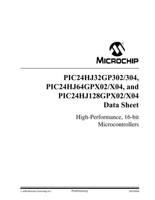
Figure 1-1 shows a general block diagram of the<br />
core and peripheral modules in the<br />
PIC24HJ32GP302/304, <strong>PIC24HJ64</strong>GPX02/X04, and<br />
PIC24HJ128GPX02/X04 families of devices.<br />
Table 1-1 lists the functions of the various pins<br />
shown in the pinout diagrams.<br />
© 2008 Microchip Technology Inc. Preliminary DS70293B-page 9
PIC24HJ32GP302/304, <strong>PIC24HJ64</strong>GPX02/X04, AND PIC24HJ128GPX02/X04<br />
FIGURE 1-1:<br />
PIC24HJ32GP302/304, <strong>PIC24HJ64</strong>GPX02/X04, AND PIC24HJ128GPX02/X04<br />
BLOCK DIAGRAM<br />
PSV and Table<br />
Data Access<br />
Control Block<br />
Interrupt<br />
Controller<br />
X Data Bus<br />
PORTA<br />
8<br />
16<br />
16<br />
16<br />
23<br />
23<br />
Address Latch<br />
23<br />
PCU PCH PCL<br />
Program Counter<br />
Stack Loop<br />
Control Control<br />
Logic Logic<br />
Data Latch<br />
X RAM<br />
Address<br />
Latch<br />
16<br />
Address Generator Units<br />
DMA<br />
RAM<br />
DMA<br />
Controller<br />
16<br />
PORTB<br />
PORTC<br />
Program Memory<br />
Data Latch<br />
Address Bus<br />
24<br />
ROM Latch<br />
EA MUX<br />
16 16<br />
Remappable<br />
Pins<br />
Instruction<br />
Decode and<br />
Control<br />
Instruction Reg<br />
Literal Data<br />
16<br />
Control Signals<br />
to Various Blocks<br />
17 x 17 Multiplier<br />
OSC2/CLKO<br />
OSC1/CLKI<br />
Timing<br />
Generation<br />
FRC/LPRC<br />
Oscillators<br />
Precision<br />
Band Gap<br />
Reference<br />
Voltage<br />
Regulator<br />
Power-up<br />
Timer<br />
Oscillator<br />
Start-up Timer<br />
Power-on<br />
Reset<br />
Watchdog<br />
Timer<br />
Brown-out<br />
Reset<br />
Divide Support<br />
16 x 16<br />
W Register Array<br />
16-bit ALU<br />
16<br />
16<br />
VDDCORE/VCAP<br />
VDD, VSS<br />
MCLR<br />
PMP/<br />
EPSP<br />
Comparator1,<br />
2<br />
ECAN1<br />
Timers<br />
1-5<br />
UART1, 2<br />
ADC1<br />
OC/<br />
PWM1-4<br />
RTCC<br />
SPI1, 2<br />
IC1, 2, 7, 8<br />
CNx<br />
I2C1<br />
Note:<br />
Not all pins or features are implemented on all device pinout configurations. See pinout diagrams for the specific pins and features<br />
present on each device.<br />
DS70293B-page 10 Preliminary © 2008 Microchip Technology Inc.
PIC24HJ32GP302/304, <strong>PIC24HJ64</strong>GPX02/X04, AND PIC24HJ128GPX02/X04<br />
TABLE 1-1:<br />
Pin Name<br />
PINOUT I/O DESCRIPTIONS<br />
Pin<br />
Type<br />
Buffer<br />
Type<br />
AN0-AN12 I Analog Analog input channels.<br />
CLKI<br />
CLKO<br />
OSC1<br />
OSC2<br />
SOSCI<br />
SOSCO<br />
I<br />
O<br />
I<br />
I/O<br />
I<br />
O<br />
ST/CMOS<br />
—<br />
ST/CMOS<br />
—<br />
ST/CMOS<br />
—<br />
Description<br />
External clock source input. Always associated with OSC1 pin function.<br />
Oscillator crystal output. Connects to crystal or resonator in Crystal Oscillator<br />
mode. Optionally functions as CLKO in RC and EC modes. Always<br />
associated with OSC2 pin function.<br />
Oscillator crystal input. ST buffer when configured in RC mode; CMOS<br />
otherwise.<br />
Oscillator crystal output. Connects to crystal or resonator in Crystal Oscillator<br />
mode. Optionally functions as CLKO in RC and EC modes.<br />
32.768 kHz low-power oscillator crystal input; CMOS otherwise.<br />
32.768 kHz low-power oscillator crystal output.<br />
CN0-CN30 I ST Change notification inputs.<br />
Can be software programmed for internal weak pull-ups on all inputs.<br />
IC1-IC2<br />
IC7-IC8<br />
OCFA<br />
OC1-OC4<br />
INT0<br />
INT1<br />
INT2<br />
RA0-RA4<br />
RA7-RA10<br />
I<br />
I<br />
I<br />
O<br />
I<br />
I<br />
I<br />
I/O<br />
I/O<br />
ST<br />
ST<br />
ST<br />
—<br />
ST<br />
ST<br />
ST<br />
ST<br />
ST<br />
Capture inputs 1/2<br />
Capture inputs 7/8.<br />
Compare Fault A input (for Compare Channels 1, 2, 3 and 4).<br />
Compare outputs 1 through 4.<br />
External interrupt 0.<br />
External interrupt 1.<br />
External interrupt 2.<br />
PORTA is a bidirectional I/O port.<br />
PORTA is a bidirectional I/O port.<br />
RB0-RB15 I/O ST PORTB is a bidirectional I/O port.<br />
RC0-RC9 I/O ST PORTC is a bidirectional I/O port.<br />
T1CK<br />
T2CK<br />
T3CK<br />
T4CK<br />
T5CK<br />
U1CTS<br />
U1RTS<br />
U1RX<br />
U1TX<br />
U2CTS<br />
U2RTS<br />
U2RX<br />
U2TX<br />
SCK1<br />
SDI1<br />
SDO1<br />
SS1<br />
SCK2<br />
SDI2<br />
SDO2<br />
SS2<br />
SCL1<br />
SDA1<br />
ASCL1<br />
ASDA1<br />
I<br />
I<br />
I<br />
I<br />
I<br />
I<br />
O<br />
I<br />
O<br />
I<br />
O<br />
I<br />
O<br />
I/O<br />
I<br />
O<br />
I/O<br />
I/O<br />
I<br />
O<br />
I/O<br />
I/O<br />
I/O<br />
I/O<br />
I/O<br />
ST<br />
ST<br />
ST<br />
ST<br />
ST<br />
ST<br />
—<br />
ST<br />
—<br />
ST<br />
—<br />
ST<br />
—<br />
ST<br />
ST<br />
—<br />
ST<br />
ST<br />
ST<br />
—<br />
ST<br />
ST<br />
ST<br />
ST<br />
ST<br />
Timer1 external clock input.<br />
Timer2 external clock input.<br />
Timer3 external clock input.<br />
Timer4 external clock input.<br />
Timer5 external clock input.<br />
UART1 clear to send.<br />
UART1 ready to send.<br />
UART1 receive.<br />
UART1 transmit.<br />
UART2 clear to send.<br />
UART2 ready to send.<br />
UART2 receive.<br />
UART2 transmit.<br />
Synchronous serial clock input/output for SPI1.<br />
SPI1 data in.<br />
SPI1 data out.<br />
SPI1 slave synchronization or frame pulse I/O.<br />
Synchronous serial clock input/output for SPI2.<br />
SPI2 data in.<br />
SPI2 data out.<br />
SPI2 slave synchronization or frame pulse I/O.<br />
Synchronous serial clock input/output for I2C1.<br />
Synchronous serial data input/output for I2C1.<br />
Alternate synchronous serial clock input/output for I2C1.<br />
Alternate synchronous serial data input/output for I2C1.<br />
Legend: CMOS = CMOS compatible input or output Analog = Analog input P = Power<br />
ST = Schmitt Trigger input with CMOS levels O = Output I = Input<br />
TTL = TTL input buffer<br />
© 2008 Microchip Technology Inc. Preliminary DS70293B-page 11
PIC24HJ32GP302/304, <strong>PIC24HJ64</strong>GPX02/X04, AND PIC24HJ128GPX02/X04<br />
TABLE 1-1:<br />
TMS<br />
TCK<br />
TDI<br />
TDO<br />
C1RX<br />
C1TX<br />
I<br />
I<br />
I<br />
O<br />
I<br />
O<br />
ST<br />
ST<br />
ST<br />
—<br />
ST<br />
—<br />
JTAG Test mode select pin.<br />
JTAG test clock input pin.<br />
JTAG test data input pin.<br />
JTAG test data output pin.<br />
ECAN1 bus receive pin.<br />
ECAN1 bus transmit pin.<br />
RTCC O — Real-Time Clock Alarm Output.<br />
CVREF O ANA Comparator Voltage Reference Output.<br />
C1IN-<br />
C1IN+<br />
C1OUT<br />
C2IN-<br />
C2IN+<br />
C2OUT<br />
PMA0<br />
PMA1<br />
Pin Name<br />
PMA2 -PMPA10<br />
PMBE<br />
PMCS1<br />
PMD0-PMPD7<br />
PMRD<br />
PMWR<br />
PGD1/EMUD1<br />
PGC1/EMUC1<br />
PGD2/EMUD2<br />
PGC2/EMUC2<br />
PGD3/EMUD3<br />
PGC3/EMUC3<br />
PINOUT I/O DESCRIPTIONS (CONTINUED)<br />
Pin<br />
Type<br />
I<br />
I<br />
O<br />
I<br />
I<br />
O<br />
I/O<br />
I/O<br />
O<br />
O<br />
O<br />
I/O<br />
O<br />
O<br />
I/O<br />
I<br />
I/O<br />
I<br />
I/O<br />
I<br />
Buffer<br />
Type<br />
ANA<br />
ANA<br />
—<br />
ANA<br />
ANA<br />
—<br />
TTL/ST<br />
TTL/ST<br />
—<br />
—<br />
—<br />
TTL/ST<br />
—<br />
—<br />
ST<br />
ST<br />
ST<br />
ST<br />
ST<br />
ST<br />
Comparator 1 Negative Input.<br />
Comparator 1 Positive Input.<br />
Comparator 1 Output.<br />
Comparator 2 Negative Input.<br />
Comparator 2 Positive Input.<br />
Comparator 2 Output.<br />
Description<br />
Parallel Master Port Address Bit 0 Input (Buffered Slave modes) and Output<br />
(Master modes).<br />
Parallel Master Port Address Bit 1 Input (Buffered Slave modes) and Output<br />
(Master modes).<br />
Parallel Master Port Address (Demultiplexed Master Modes).<br />
Parallel Master Port Byte Enable Strobe.<br />
Parallel Master Port Chip Select 1 Strobe.<br />
Parallel Master Port Data (Demultiplexed Master mode) or Address/Data<br />
(Multiplexed Master modes).<br />
Parallel Master Port Read Strobe.<br />
Parallel Master Port Write Strobe.<br />
Data I/O pin for programming/debugging communication channel 1.<br />
Clock input pin for programming/debugging communication channel 1.<br />
Data I/O pin for programming/debugging communication channel 2.<br />
Clock input pin for programming/debugging communication channel 2.<br />
Data I/O pin for programming/debugging communication channel 3.<br />
Clock input pin for programming/debugging communication channel 3.<br />
MCLR I/P ST Master Clear (Reset) input. This pin is an active-low Reset to the device.<br />
AVDD P P Positive supply for analog modules.<br />
AVSS P P Ground reference for analog modules.<br />
VDD P — Positive supply for peripheral logic and I/O pins.<br />
VDDCORE P — CPU logic filter capacitor connection.<br />
Vss P — Ground reference for logic and I/O pins.<br />
VREF+ I Analog Analog voltage reference (high) input.<br />
VREF- I Analog Analog voltage reference (low) input.<br />
Legend: CMOS = CMOS compatible input or output Analog = Analog input P = Power<br />
ST = Schmitt Trigger input with CMOS levels O = Output I = Input<br />
TTL = TTL input buffer<br />
DS70293B-page 12 Preliminary © 2008 Microchip Technology Inc.
PIC24HJ32GP302/304, <strong>PIC24HJ64</strong>GPX02/X04, AND PIC24HJ128GPX02/X04<br />
2.0 CPU<br />
Note:<br />
This data sheet summarizes the features<br />
of the PIC24HJ32GP302/304,<br />
<strong>PIC24HJ64</strong>GPX02/X04,<br />
and<br />
PIC24HJ128GPX02/X04 families of<br />
devices. It is not intended to be a<br />
comprehensive reference source. To<br />
complement the information in this data<br />
sheet, refer to the PIC24H Family<br />
Reference Manual, “Section 2. CPU”<br />
(DS70245), which is available from the<br />
Microchip website (www.microchip.com).<br />
2.1 Overview<br />
The PIC24HJ32GP302/304, <strong>PIC24HJ64</strong>GPX02/X04,<br />
and PIC24HJ128GPX02/X04 CPU module has a 16-bit<br />
(data) modified Harvard architecture with an enhanced<br />
instruction set and addressing modes. The CPU has a<br />
24-bit instruction word with a variable length opcode<br />
field. The Program Counter (PC) is 23 bits wide and<br />
addresses up to 4M x 24 bits of user program memory<br />
space. The actual amount of program memory<br />
implemented varies by device. A single-cycle<br />
instruction prefetch mechanism is used to help<br />
maintain throughput and provides predictable<br />
execution. All instructions execute in a single cycle,<br />
with the exception of instructions that change the<br />
program flow, the double word move (MOV.D)<br />
instruction and the table instructions. Overhead-free,<br />
single-cycle program loop constructs are supported<br />
using the REPEAT instruction, which is interruptible at<br />
any point.<br />
The PIC24HJ32GP302/304, <strong>PIC24HJ64</strong>GPX02/X04,<br />
and PIC24HJ128GPX02/X04 devices have sixteen,<br />
16-bit working registers in the programmer’s model.<br />
Each of the working registers can serve as a data,<br />
address or address offset register. The 16th working<br />
register (W15) operates as a software Stack Pointer<br />
(SP) for interrupts and calls.<br />
The PIC24HJ32GP302/304, <strong>PIC24HJ64</strong>GPX02/X04,<br />
and PIC24HJ128GPX02/X04 instruction set includes<br />
many addressing modes and is designed for optimum<br />
C compiler efficiency. For most instructions, the<br />
PIC24HJ32GP302/304, <strong>PIC24HJ64</strong>GPX02/X04, and<br />
PIC24HJ128GPX02/X04 is capable of executing a<br />
data (or program data) memory read, a working register<br />
(data) read, a data memory write and a program<br />
(instruction) memory read per instruction cycle. As a<br />
result, three parameter instructions can be supported,<br />
allowing A + B = C operations to be executed in a single<br />
cycle.<br />
A block diagram of the CPU is shown in Figure 2-1, and<br />
the programmer’s model for the PIC24HJ32GP302/<br />
304, <strong>PIC24HJ64</strong>GPX02/X04, and<br />
PIC24HJ128GPX02/X04 is shown in Figure 2-2.<br />
2.2 Data Addressing Overview<br />
The data space can be linearly addressed as 32K words<br />
or 64 Kbytes using an Address Generation Unit (AGU).<br />
The upper 32 Kbytes of the data space memory map can<br />
optionally be mapped into program space at any 16K<br />
program word boundary defined by the 8-bit Program<br />
Space Visibility Page (PSVPAG) register. The program<br />
to data space mapping feature lets any instruction<br />
access program space as if it were data space.<br />
The data space also includes 2 Kbytes of DMA RAM,<br />
which is primarily used for DMA data transfers, but may<br />
be used as general purpose RAM.<br />
© 2008 Microchip Technology Inc. Preliminary DS70293B-page 13
PIC24HJ32GP302/304, <strong>PIC24HJ64</strong>GPX02/X04, AND PIC24HJ128GPX02/X04<br />
2.3 Special MCU Features<br />
The PIC24HJ32GP302/304, <strong>PIC24HJ64</strong>GPX02/X04,<br />
and PIC24HJ128GPX02/X04 features a 17-bit by 17-<br />
bit, single-cycle multiplier. The multiplier can perform<br />
signed, unsigned and mixed-sign multiplication. Using<br />
a 17-bit by 17-bit multiplier for 16-bit by 16-bit<br />
multiplication makes mixed-sign multiplication<br />
possible.<br />
The PIC24HJ32GP302/304, <strong>PIC24HJ64</strong>GPX02/X04,<br />
and PIC24HJ128GPX02/X04 devices support 16/16<br />
and 32/16 integer divide operations. All divide<br />
instructions are iterative operations. They must be<br />
executed within a REPEAT loop, resulting in a total<br />
execution time of 19 instruction cycles. The divide<br />
operation can be interrupted during any of those<br />
19 cycles without loss of data.<br />
A multi-bit data shifter is used to perform up to a 16-bit,<br />
left or right shift in a single cycle.<br />
FIGURE 2-1:<br />
PIC24HJ32GP302/304, <strong>PIC24HJ64</strong>GPX02/X04, AND PIC24HJ128GPX02/X04 CPU<br />
CORE BLOCK DIAGRAM<br />
PSV & Table<br />
Data Access<br />
Control Block<br />
Interrupt<br />
Controller<br />
X Data Bus<br />
8<br />
16<br />
16<br />
16<br />
23<br />
23<br />
PCU PCH PCL<br />
Program Counter<br />
Stack Loop<br />
Control Control<br />
Logic Logic<br />
Data Latch<br />
X RAM<br />
Address<br />
Latch<br />
DMA<br />
RAM<br />
16<br />
23<br />
16<br />
DMA<br />
Address Latch<br />
Address Generator Units<br />
Controller<br />
Program Memory<br />
Address Bus<br />
EA MUX<br />
Data Latch<br />
24<br />
ROM Latch<br />
16 16<br />
Instruction<br />
Decode &<br />
Control<br />
Instruction Reg<br />
Literal Data<br />
16<br />
Control Signals<br />
to Various Blocks<br />
17 x 17 Multiplier<br />
Divide Support<br />
16 x 16<br />
W Register Array<br />
16<br />
16-bit ALU<br />
16<br />
To Peripheral Modules<br />
DS70293B-page 14 Preliminary © 2008 Microchip Technology Inc.
PIC24HJ32GP302/304, <strong>PIC24HJ64</strong>GPX02/X04, AND PIC24HJ128GPX02/X04<br />
FIGURE 2-2:<br />
PIC24HJ32GP302/304, <strong>PIC24HJ64</strong>GPX02/X04, AND PIC24HJ128GPX02/X04<br />
PROGRAMMER’S MODEL<br />
D15<br />
D0<br />
W0/WREG<br />
W1<br />
W2<br />
PUSH.S Shadow<br />
Legend<br />
W3<br />
W4<br />
W5<br />
W6<br />
W7<br />
W8<br />
Working Registers<br />
W9<br />
W10<br />
W11<br />
W12<br />
W13<br />
W14/Frame Pointer<br />
W15/Stack Pointer<br />
SPLIM<br />
Stack Pointer Limit Register<br />
PC22<br />
PC0<br />
0<br />
Program Counter<br />
7 0<br />
TBLPAG<br />
Data Table Page Address<br />
7 0<br />
PSVPAG<br />
Program Space Visibility Page Address<br />
15 0<br />
RCOUNT<br />
REPEAT Loop Counter<br />
15 0<br />
CORCON<br />
Core Configuration Register<br />
— — — —<br />
— —<br />
— DC IPL2 IPL1 IPL0 RA N<br />
OV<br />
Z<br />
C<br />
STATUS Register<br />
SRH<br />
SRL<br />
© 2008 Microchip Technology Inc. Preliminary DS70293B-page 15
PIC24HJ32GP302/304, <strong>PIC24HJ64</strong>GPX02/X04, AND PIC24HJ128GPX02/X04<br />
2.4 CPU Control Registers<br />
REGISTER 2-1:<br />
SR: CPU STATUS REGISTER<br />
U-0 U-0 U-0 U-0 U-0 U-0 U-0 R/W-0<br />
— — — — — — — DC<br />
bit 15 bit 8<br />
R/W-0 (1) R/W-0 (2) R/W-0 (2) R-0 R/W-0 R/W-0 R/W-0 R/W-0<br />
IPL (2) RA N OV Z C<br />
bit 7 bit 0<br />
Legend:<br />
C = Clear only bit R = Readable bit U = Unimplemented bit, read as ‘0’<br />
S = Set only bit W = Writable bit -n = Value at POR<br />
‘1’ = Bit is set ‘0’ = Bit is cleared x = Bit is unknown<br />
bit 15-9 Unimplemented: Read as ‘0’<br />
bit 8<br />
DC: MCU ALU Half Carry/Borrow bit<br />
1 = A carry-out from the 4th low-order bit (for byte-sized data) or 8th low-order bit (for word-sized data)<br />
of the result occurred<br />
0 = No carry-out from the 4th low-order bit (for byte-sized data) or 8th low-order bit (for word-sized<br />
data) of the result occurred<br />
bit 7-5 IPL: CPU Interrupt Priority Level Status bits (2)<br />
bit 4<br />
bit 3<br />
bit 2<br />
bit 1<br />
bit 0<br />
111 = CPU Interrupt Priority Level is 7 (15), user interrupts disabled<br />
110 = CPU Interrupt Priority Level is 6 (14)<br />
101 = CPU Interrupt Priority Level is 5 (13)<br />
100 = CPU Interrupt Priority Level is 4 (12)<br />
011 = CPU Interrupt Priority Level is 3 (11)<br />
010 = CPU Interrupt Priority Level is 2 (10)<br />
001 = CPU Interrupt Priority Level is 1 (9)<br />
000 = CPU Interrupt Priority Level is 0 (8)<br />
RA: REPEAT Loop Active bit<br />
1 = REPEAT loop in progress<br />
0 = REPEAT loop not in progress<br />
N: MCU ALU Negative bit<br />
1 = Result was negative<br />
0 = Result was non-negative (zero or positive)<br />
OV: MCU ALU Overflow bit<br />
This bit is used for signed arithmetic (two’s complement). It indicates an overflow of a magnitude that<br />
causes the sign bit to change state.<br />
1 = Overflow occurred for signed arithmetic (in this arithmetic operation)<br />
0 = No overflow occurred<br />
Z: MCU ALU Zero bit<br />
1 = An operation that affects the Z bit has set it at some time in the past<br />
0 = The most recent operation that affects the Z bit has cleared it (i.e., a non-zero result)<br />
C: MCU ALU Carry/Borrow bit<br />
1 = A carry-out from the Most Significant bit of the result occurred<br />
0 = No carry-out from the Most Significant bit of the result occurred<br />
Note 1: The IPL bits are concatenated with the IPL bit (CORCON) to form the CPU Interrupt Priority<br />
Level. The value in parentheses indicates the IPL if IPL = 1. User interrupts are disabled when<br />
IPL = 1.<br />
2: The IPL Status bits are read only when NSTDIS = 1 (INTCON1).<br />
DS70293B-page 16 Preliminary © 2008 Microchip Technology Inc.
PIC24HJ32GP302/304, <strong>PIC24HJ64</strong>GPX02/X04, AND PIC24HJ128GPX02/X04<br />
REGISTER 2-2:<br />
CORCON: CORE CONTROL REGISTER<br />
U-0 U-0 U-0 U-0 U-0 U-0 U-0 U-0<br />
— — — — — — — —<br />
bit 15 bit 8<br />
U-0 U-0 U-0 U-0 R/C-0 R/W-0 U-0 U-0<br />
— — — — IPL3 (1) PSV — —<br />
bit 7 bit 0<br />
Legend:<br />
C = Clear only bit<br />
R = Readable bit W = Writable bit -n = Value at POR ‘1’ = Bit is set<br />
0’ = Bit is cleared ‘x = Bit is unknown U = Unimplemented bit, read as ‘0’<br />
bit 15-4 Unimplemented: Read as ‘0’<br />
bit 3 IPL3: CPU Interrupt Priority Level Status bit 3 (1)<br />
1 = CPU interrupt priority level is greater than 7<br />
0 = CPU interrupt priority level is 7 or less<br />
bit 2<br />
PSV: Program Space Visibility in Data Space Enable bit<br />
1 = Program space visible in data space<br />
0 = Program space not visible in data space<br />
bit 1-0 Unimplemented: Read as ‘0’<br />
Note 1:<br />
The IPL3 bit is concatenated with the IPL bits (SR) to form the CPU interrupt priority level.<br />
© 2008 Microchip Technology Inc. Preliminary DS70293B-page 17
PIC24HJ32GP302/304, <strong>PIC24HJ64</strong>GPX02/X04, AND PIC24HJ128GPX02/X04<br />
2.5 Arithmetic Logic Unit (ALU)<br />
The PIC24HJ32GP302/304, <strong>PIC24HJ64</strong>GPX02/X04,<br />
and PIC24HJ128GPX02/X04 ALU is 16 bits wide and<br />
is capable of addition, subtraction, bit shifts and logic<br />
operations. Unless otherwise mentioned, arithmetic<br />
operations are two’s complement in nature. Depending<br />
on the operation, the ALU can affect the values of the<br />
Carry (C), Zero (Z), Negative (N), Overflow (OV) and<br />
Digit Carry (DC) Status bits in the SR register. The C<br />
and DC Status bits operate as Borrow and Digit Borrow<br />
bits, respectively, for subtraction operations.<br />
The ALU can perform 8-bit or 16-bit operations,<br />
depending on the mode of the instruction that is used.<br />
Data for the ALU operation can come from the W<br />
register array or data memory, depending on the<br />
addressing mode of the instruction. Likewise, output<br />
data from the ALU can be written to the W register array<br />
or a data memory location.<br />
Refer to the “dsPIC30F/33F Programmer’s Reference<br />
Manual” (DS70157) for information on the SR bits<br />
affected by each instruction.<br />
The PIC24HJ32GP302/304, <strong>PIC24HJ64</strong>GPX02/X04,<br />
and PIC24HJ128GPX02/X04 CPU incorporates hardware<br />
support for both multiplication and division. This<br />
includes a dedicated hardware multiplier and support<br />
hardware for 16-bit-divisor division.<br />
2.5.1 MULTIPLIER<br />
Using the high-speed 17-bit x 17-bit multiplier, the ALU<br />
supports unsigned, signed or mixed-sign operation in<br />
several MCU multiplication modes:<br />
• 16-bit x 16-bit signed<br />
• 16-bit x 16-bit unsigned<br />
• 16-bit signed x 5-bit (literal) unsigned<br />
• 16-bit unsigned x 16-bit unsigned<br />
• 16-bit unsigned x 5-bit (literal) unsigned<br />
• 16-bit unsigned x 16-bit signed<br />
• 8-bit unsigned x 8-bit unsigned<br />
2.5.2 DIVIDER<br />
The divide block supports 32-bit/16-bit and 16-bit/16-bit<br />
signed and unsigned integer divide operations with the<br />
following data sizes:<br />
1. 32-bit signed/16-bit signed divide<br />
2. 32-bit unsigned/16-bit unsigned divide<br />
3. 16-bit signed/16-bit signed divide<br />
4. 16-bit unsigned/16-bit unsigned divide<br />
The quotient for all divide instructions ends up in W0<br />
and the remainder in W1. 16-bit signed and unsigned<br />
DIV instructions can specify any W register for both<br />
the 16-bit divisor (Wn) and any W register (aligned)<br />
pair (W(m + 1):Wm) for the 32-bit dividend. The divide<br />
algorithm takes one cycle per bit of divisor, so both<br />
32-bit/16-bit and 16-bit/16-bit instructions take the<br />
same number of cycles to execute.<br />
2.5.3 MULTI-BIT DATA SHIFTER<br />
The multi-bit data shifter is capable of performing up to<br />
16-bit arithmetic or logic right shifts, or up to 16-bit left<br />
shifts in a single cycle. The source can be either a<br />
working register or a memory location.<br />
The shifter requires a signed binary value to determine<br />
both the magnitude (number of bits) and direction of the<br />
shift operation. A positive value shifts the operand right.<br />
A negative value shifts the operand left. A value of ‘0’<br />
does not modify the operand.<br />
DS70293B-page 18 Preliminary © 2008 Microchip Technology Inc.
PIC24HJ32GP302/304, <strong>PIC24HJ64</strong>GPX02/X04, AND PIC24HJ128GPX02/X04<br />
3.0 MEMORY ORGANIZATION<br />
Note: This data sheet summarizes the features<br />
of the PIC24HJ32GP302/304,<br />
<strong>PIC24HJ64</strong>GPX02/X04,<br />
and<br />
PIC24HJ128GPX02/X04 families of<br />
devices. It is not intended to be a comprehensive<br />
reference source. To complement<br />
the information in this data sheet, refer to<br />
the PIC24H Family Reference Manual,<br />
“Section 4. Program Memory”<br />
(DS70238), which is available from the<br />
Microchip website (www.microchip.com).<br />
The PIC24HJ32GP302/304, <strong>PIC24HJ64</strong>GPX02/X04,<br />
and PIC24HJ128GPX02/X04 architecture features<br />
separate program and data memory spaces and<br />
buses. This architecture also allows the direct access<br />
of program memory from the data space during code<br />
execution.<br />
3.1 Program Address Space<br />
The program address memory space of the<br />
PIC24HJ32GP302/304, <strong>PIC24HJ64</strong>GPX02/X04, and<br />
PIC24HJ128GPX02/X04 devices is 4M instructions.<br />
The space is addressable by a 24-bit value derived<br />
either from the 23-bit Program Counter (PC) during<br />
program execution, or from table operation or data<br />
space remapping as described in Section 3.4<br />
“Interfacing Program and Data Memory Spaces”.<br />
User application access to the program memory space<br />
is restricted to the lower half of the address range<br />
(0x000000 to 0x7FFFFF). The exception is the use of<br />
TBLRD/TBLWT operations, which use TBLPAG to<br />
permit access to the Configuration bits and Device ID<br />
sections of the configuration memory space.<br />
The memory map for the PIC24HJ32GP302/304,<br />
<strong>PIC24HJ64</strong>GPX02/X04, and PIC24HJ128GPX02/X04<br />
devices is shown in Figure 3-1.<br />
FIGURE 3-1:<br />
PROGRAM MEMORY MAP FOR PIC24HJ32GP302/304, <strong>PIC24HJ64</strong>GPX02/X04,<br />
AND PIC24HJ128GPX02/X04 DEVICES<br />
Configuration Memory Space User Memory Space<br />
Note:<br />
PIC24HJ32GP302/304<br />
GOTO Instruction<br />
Reset Address<br />
Interrupt Vector Table<br />
Reserved<br />
Alternate Vector Table<br />
User Program<br />
Flash Memory<br />
(11264 instructions)<br />
Unimplemented<br />
(Read ‘0’s)<br />
Reserved<br />
Device Configuration<br />
Registers<br />
Reserved<br />
DEVID (2)<br />
Memory areas are not shown to scale.<br />
<strong>PIC24HJ64</strong>GPX02/X04<br />
GOTO Instruction<br />
Reset Address<br />
Interrupt Vector Table<br />
Reserved<br />
Alternate Vector Table<br />
User Program<br />
Flash Memory<br />
(22016 instructions)<br />
Unimplemented<br />
(Read ‘0’s)<br />
Reserved<br />
Device Configuration<br />
Registers<br />
Reserved<br />
DEVID (2)<br />
PIC24HJ128GPX02/X04<br />
GOTO Instruction<br />
Reset Address<br />
Interrupt Vector Table<br />
Reserved<br />
Alternate Vector Table<br />
User Program<br />
Flash Memory<br />
(44032 instructions)<br />
Unimplemented<br />
(Read ‘0’s)<br />
Reserved<br />
Device Configuration<br />
Registers<br />
Reserved<br />
DEVID (2)<br />
Reserved Reserved Reserved<br />
0x000000<br />
0x000002<br />
0x000004<br />
0x0000FE<br />
0x000100<br />
0x000104<br />
0x0001FE<br />
0x000200<br />
0x0057FE<br />
0x005800<br />
0x00ABFE<br />
0x00AC00<br />
0x0157FE<br />
0x015800<br />
0x7FFFFE<br />
0x800000<br />
0xF7FFFE<br />
0xF80000<br />
0xF80017<br />
0xF80018<br />
0xFEFFFE<br />
0xFF0000<br />
0xFF0002<br />
0xFFFFFE<br />
© 2008 Microchip Technology Inc. Preliminary DS70293B-page 19
PIC24HJ32GP302/304, <strong>PIC24HJ64</strong>GPX02/X04, AND PIC24HJ128GPX02/X04<br />
3.1.1 PROGRAM MEMORY<br />
ORGANIZATION<br />
The program memory space is organized in wordaddressable<br />
blocks. Although it is treated as 24 bits<br />
wide, it is more appropriate to think of each address of<br />
the program memory as a lower and upper word, with<br />
the upper byte of the upper word being unimplemented.<br />
The lower word always has an even address, while the<br />
upper word has an odd address (Figure 3-2).<br />
Program memory addresses are always word-aligned<br />
on the lower word, and addresses are incremented or<br />
decremented by two during code execution. This<br />
arrangement provides compatibility with data memory<br />
space addressing and makes data in the program<br />
memory space accessible.<br />
3.1.2 INTERRUPT AND TRAP VECTORS<br />
All PIC24HJ32GP302/304, <strong>PIC24HJ64</strong>GPX02/X04,<br />
and PIC24HJ128GPX02/X04 devices reserve the<br />
addresses between 0x00000 and 0x000200 for hardcoded<br />
program execution vectors. A hardware Reset<br />
vector is provided to redirect code execution from the<br />
default value of the PC on device Reset to the actual<br />
start of code. A GOTO instruction is programmed by the<br />
user application at 0x000000, with the actual address<br />
for the start of code at 0x000002.<br />
PIC24HJ32GP302/304, <strong>PIC24HJ64</strong>GPX02/X04, and<br />
PIC24HJ128GPX02/X04 devices also have two<br />
interrupt vector tables, located from 0x000004 to<br />
0x0000FF and 0x000100 to 0x0001FF. These vector<br />
tables allow each of the device interrupt sources to be<br />
handled by separate Interrupt Service Routines (ISRs).<br />
A more detailed discussion of the interrupt vector<br />
tables is provided in Section 6.1 “Interrupt Vector<br />
Table”.<br />
FIGURE 3-2:<br />
PROGRAM MEMORY ORGANIZATION<br />
msw<br />
Address<br />
most significant word<br />
least significant word<br />
PC Address<br />
(lsw Address)<br />
0x000001<br />
0x000003<br />
0x000005<br />
0x000007<br />
23<br />
00000000<br />
00000000<br />
00000000<br />
00000000<br />
16<br />
8<br />
0<br />
0x000000<br />
0x000002<br />
0x000004<br />
0x000006<br />
Program Memory<br />
‘Phantom’ Byte<br />
(read as ‘0’)<br />
Instruction Width<br />
DS70293B-page 20 Preliminary © 2008 Microchip Technology Inc.
PIC24HJ32GP302/304, <strong>PIC24HJ64</strong>GPX02/X04, AND PIC24HJ128GPX02/X04<br />
3.2 Data Address Space<br />
The PIC24HJ32GP302/304, <strong>PIC24HJ64</strong>GPX02/X04,<br />
and PIC24HJ128GPX02/X04 CPU has a separate 16-<br />
bit-wide data memory space. The data space is<br />
accessed using separate Address Generation Units<br />
(AGUs) for read and write operations. The data<br />
memory maps are shown in Figure 3-3 and Figure 3-4.<br />
All Effective Addresses (EAs) in the data memory space<br />
are 16 bits wide and point to bytes within the data space.<br />
This arrangement gives a data space address range of<br />
64 Kbytes or 32K words. The lower half of the data<br />
memory space (that is, when EA = 0) is used for<br />
implemented memory addresses, while the upper half<br />
(EA = 1) is reserved for the Program Space<br />
Visibility area (see Section 3.4.3 “Reading Data From<br />
Program Memory Using Program Space Visibility”).<br />
PIC24HJ32GP302/304, <strong>PIC24HJ64</strong>GPX02/X04, and<br />
PIC24HJ128GPX02/X04 devices implement up to<br />
8 Kbytes of data memory. Should an EA point to a location<br />
outside of this area, an all-zero word or byte is<br />
returned.<br />
3.2.1 DATA SPACE WIDTH<br />
The data memory space is organized in byte<br />
addressable, 16-bit wide blocks. Data is aligned in data<br />
memory and registers as 16-bit words, but all data<br />
space EAs resolve to bytes. The Least Significant<br />
Bytes (LSBs) of each word have even addresses, while<br />
the Most Significant Bytes (MSBs) have odd<br />
addresses.<br />
3.2.2 DATA MEMORY ORGANIZATION<br />
AND ALIGNMENT<br />
To maintain backward compatibility with PIC ® MCU<br />
devices and improve data space memory usage<br />
efficiency, the PIC24HJ32GP302/304,<br />
<strong>PIC24HJ64</strong>GPX02/X04, and PIC24HJ128GPX02/X04<br />
instruction set supports both word and byte operations.<br />
As a consequence of byte accessibility, all effective<br />
address calculations are internally scaled to step<br />
through word-aligned memory. For example, the core<br />
recognizes that Post-Modified Register Indirect<br />
Addressing mode [Ws++] results in a value of Ws + 1<br />
for byte operations and Ws + 2 for word operations.<br />
A data byte read, reads the complete word that<br />
contains the byte, using the LSB of any EA to<br />
determine which byte to select. The selected byte is<br />
placed onto the LSB of the data path. That is, data<br />
memory and registers are organized as two parallel<br />
byte-wide entities with shared (word) address decode<br />
but separate write lines. Data byte writes only write to<br />
the corresponding side of the array or register that<br />
matches the byte address.<br />
All word accesses must be aligned to an even address.<br />
Misaligned word data fetches are not supported, so<br />
care must be taken when mixing byte and word<br />
operations, or translating from 8-bit MCU code. If a<br />
misaligned read or write is attempted, an address error<br />
trap is generated. If the error occurred on a read, the<br />
instruction underway is completed. If the error occurred<br />
on a write, the instruction is executed but the write does<br />
not occur. In either case, a trap is then executed,<br />
allowing the system and/or user application to examine<br />
the machine state prior to execution of the address<br />
Fault.<br />
All byte loads into any W register are loaded into the<br />
Least Significant Byte. The Most Significant Byte is not<br />
modified.<br />
A sign-extend instruction (SE) is provided to allow user<br />
applications to translate 8-bit signed data to 16-bit<br />
signed values. Alternatively, for 16-bit unsigned data,<br />
user applications can clear the MSB of any W register<br />
by executing a zero-extend (ZE) instruction on the<br />
appropriate address.<br />
3.2.3 SFR SPACE<br />
The first 2 Kbytes of the Near Data Space, from 0x0000<br />
to 0x07FF, is primarily occupied by Special Function<br />
Registers (SFRs). These are used by the<br />
PIC24HJ32GP302/304, <strong>PIC24HJ64</strong>GPX02/X04, and<br />
PIC24HJ128GPX02/X04 core and peripheral modules<br />
for controlling the operation of the device.<br />
SFRs are distributed among the modules that they<br />
control, and are generally grouped together by module.<br />
Much of the SFR space contains unused addresses;<br />
these are read as ‘0’.<br />
Note:<br />
The actual set of peripheral features and<br />
interrupts varies by the device. Refer to<br />
the corresponding device tables and<br />
pinout diagrams for device-specific<br />
information.<br />
3.2.4 NEAR DATA SPACE<br />
The 8 Kbyte area between 0x0000 and 0x1FFF is<br />
referred to as the near data space. Locations in this<br />
space are directly addressable via a 13-bit absolute<br />
address field within all memory direct instructions.<br />
Additionally, the whole data space is addressable using<br />
MOV instructions, which support Memory Direct<br />
Addressing mode with a 16-bit address field, or by<br />
using Indirect Addressing mode using a working<br />
register as an address pointer.<br />
© 2008 Microchip Technology Inc. Preliminary DS70293B-page 21
PIC24HJ32GP302/304, <strong>PIC24HJ64</strong>GPX02/X04, AND PIC24HJ128GPX02/X04<br />
3.2.5 DMA RAM<br />
The PIC24HJ32GP302/304 devices contain 1 Kbytes<br />
of dual ported DMA RAM located at the end of X data<br />
space. The <strong>PIC24HJ64</strong>GPX02/X04 and<br />
PIC24HJ128GPX02/X04 devices contain 2 Kbytes of<br />
dual ported DMA RAM located at the end of X data<br />
space. Memory locations in the DMA RAM space are<br />
accessible simultaneously by the CPU and the DMA<br />
controller module. DMA RAM is utilized by the DMA<br />
controller to store data to be transferred to various<br />
peripherals using DMA, as well as data transferred<br />
from various peripherals using DMA. The DMA RAM<br />
can be accessed by the DMA controller without<br />
having to steal cycles from the CPU.<br />
When the CPU and the DMA controller attempt to<br />
concurrently write to the same DMA RAM location, the<br />
hardware ensures that the CPU is given precedence in<br />
accessing the DMA RAM location. Therefore, the DMA<br />
RAM provides a reliable means of transferring DMA<br />
data without ever having to stall the CPU.<br />
Note:<br />
DMA RAM can be used for general<br />
purpose data storage if the DMA function<br />
is not required in an application.<br />
FIGURE 3-3:<br />
DATA MEMORY MAP FOR PIC24HJ32GP302/304 DEVICES WITH 4 KB RAM<br />
MSb<br />
Address<br />
16 bits<br />
LSb<br />
Address<br />
2 Kbyte<br />
SFR Space<br />
0x0000<br />
0x07FF<br />
0x0801<br />
MSb<br />
SFR Space<br />
LSb<br />
0x0000<br />
0x07FE<br />
0x0800<br />
4 Kbyte<br />
SRAM Space<br />
0x13FF<br />
0x1401<br />
0x17FF<br />
0x1801<br />
X Data RAM (X)<br />
DMA RAM<br />
0x13FE<br />
0x1400<br />
0x17FE<br />
0x1800<br />
6 Kbyte<br />
Near<br />
Data<br />
Space<br />
0x8001<br />
0x8000<br />
Optionally<br />
Mapped<br />
into Program<br />
Memory<br />
X Data<br />
Unimplemented (X)<br />
0xFFFF<br />
0xFFFE<br />
DS70293B-page 22 Preliminary © 2008 Microchip Technology Inc.
PIC24HJ32GP302/304, <strong>PIC24HJ64</strong>GPX02/X04, AND PIC24HJ128GPX02/X04<br />
FIGURE 3-4:<br />
DATA MEMORY MAP FOR PIC24HJ128GP202/204, <strong>PIC24HJ64</strong>GP202/204,<br />
PIC24HJ128GP502/504, AND <strong>PIC24HJ64</strong>GP502/504 DEVICES WITH 8 KB RAM<br />
MSb<br />
Address<br />
16 bits<br />
LSb<br />
Address<br />
2 Kbyte<br />
SFR Space<br />
0x0001<br />
0x07FF<br />
0x0801<br />
MSb<br />
SFR Space<br />
LSb<br />
0x0000<br />
0x07FE<br />
0x0800<br />
8 Kbyte<br />
SRAM Space<br />
0x1FFF<br />
0x2001<br />
0x27FF<br />
0x2801<br />
X Data RAM (X)<br />
DMA RAM<br />
0x1FFE<br />
0x2000<br />
0x27FE<br />
0x2800<br />
8 Kbyte<br />
Near<br />
Data<br />
Space<br />
0x8001<br />
0x8000<br />
Optionally<br />
Mapped<br />
into Program<br />
Memory<br />
X Data<br />
Unimplemented (X)<br />
0xFFFF<br />
0xFFFE<br />
© 2008 Microchip Technology Inc. Preliminary DS70293B-page 23
PIC24HJ32GP302/304, <strong>PIC24HJ64</strong>GPX02/X04, AND PIC24HJ128GPX02/X04<br />
TABLE 3-1: CPU CORE REGISTERS MAP<br />
SFR<br />
Name<br />
SFR<br />
Addr<br />
Bit 15 Bit 14 Bit 13 Bit 12 Bit 11 Bit 10 Bit 9 Bit 8 Bit 7 Bit 6 Bit 5 Bit 4 Bit 3 Bit 2 Bit 1 Bit 0<br />
All<br />
Resets<br />
WREG0 0000 Working Register 0 0000<br />
WREG1 0002 Working Register 1 0000<br />
WREG2 0004 Working Register 2 0000<br />
WREG3 0006 Working Register 3 0000<br />
WREG4 0008 Working Register 4 0000<br />
WREG5 000A Working Register 5 0000<br />
WREG6 000C Working Register 6 0000<br />
WREG7 000E Working Register 7 0000<br />
WREG8 0010 Working Register 8 0000<br />
WREG9 0012 Working Register 9 0000<br />
WREG10 0014 Working Register 10 0000<br />
WREG11 0016 Working Register 11 0000<br />
WREG12 0018 Working Register 12 0000<br />
WREG13 001A Working Register 13 0000<br />
WREG14 001C Working Register 14 0000<br />
WREG15 001E Working Register 15 0800<br />
SPLIM 0020 Stack Pointer Limit Register xxxx<br />
PCL 002E Program Counter Low Word Register 0000<br />
PCH 0030 — — — — — — — — Program Counter High Byte Register 0000<br />
TBLPAG 0032 — — — — — — — — Table Page Address Pointer Register 0000<br />
PSVPAG 0034 — — — — — — — — Program Memory Visibility Page Address Pointer Register 0000<br />
RCOUNT 0036 Repeat Loop Counter Register xxxx<br />
SR 0042 — — — — — — — DC IPL2 IPL1 IPL0 RA N OV Z C 0000<br />
CORCON 0044 — — — — — — — — — — — — IPL3 PSV — — 0000<br />
DISICNT 0052 — — Disable Interrupts Counter Register xxxx<br />
Legend: x = unknown value on Reset, — = unimplemented, read as ‘0’. Reset values are shown in hexadecimal.<br />
DS70293B-page 24 Preliminary © 2008 Microchip Technology Inc.
PIC24HJ32GP302/304, <strong>PIC24HJ64</strong>GPX02/X04, AND PIC24HJ128GPX02/X04<br />
TABLE 3-2: CHANGE NOTIFICATION REGISTER MAP FOR PIC24HJ128GP202/502, <strong>PIC24HJ64</strong>GP202/502, AND PIC24HJ32GP302<br />
SFR<br />
Name<br />
SFR<br />
Addr<br />
Bit 15 Bit 14 Bit 13 Bit 12 Bit 11 Bit 10 Bit 9 Bit 8 Bit 7 Bit 6 Bit 5 Bit 4 Bit 3 Bit 2 Bit 1 Bit 0<br />
All<br />
Resets<br />
CNEN1 0060 CN15IE CN14IE CN13IE CN12IE CN11IE —- — — CN7IE CN6IE CN5IE CN4IE CN3IE CN2IE CN1IE CN0IE 0000<br />
CNEN2 0062 — CN30IE CN29IE — CN27IE — — CN24IE CN23IE CN22IE CN21IE — — — — CN16IE 0000<br />
CNPU1 0068 CN15PUE CN14PUE CN13PUE CN12PUE CN11PUE — — — CN7PUE CN6PUE CN5PUE CN4PUE CN3PUE CN2PUE CN1PUE CN0PUE 0000<br />
CNPU2 006A — CN30PUE CN29PUE — CN27PUE — — CN24PUE CN23PUE CN22PUE CN21PUE — — — — CN16PUE 0000<br />
Legend: x = unknown value on Reset, — = unimplemented, read as ‘0’. Reset values are shown in hexadecimal.<br />
TABLE 3-3: CHANGE NOTIFICATION REGISTER MAP FOR PIC24HJ128GP204/504, <strong>PIC24HJ64</strong>GP204/504, AND PIC24HJ32GP304<br />
SFR<br />
Name<br />
SFR<br />
Addr<br />
Bit 15 Bit 14 Bit 13 Bit 12 Bit 11 Bit 10 Bit 9 Bit 8 Bit 7 Bit 6 Bit 5 Bit 4 Bit 3 Bit 2 Bit 1 Bit 0<br />
All<br />
Resets<br />
CNEN1 0060 CN15IE CN14IE CN13IE CN12IE CN11IE CN10IE CN9IE CN8IE CN7IE CN6IE CN5IE CN4IE CN3IE CN2IE CN1IE CN0IE 0000<br />
CNEN2 00C2 — CN30IE CN29IE CN28IE CN27IE CN26IE CN25IE CN24IE CN23IE CN22IE CN21IE CN20IE CN19IE CN18IE CN17IE CN16IE 0000<br />
CNPU1 0068 CN15PUE CN14PUE CN13PUE CN12PUE CN11PUE CN10PUE CN9PUE CN8PUE CN7PUE CN6PUE CN5PUE CN4PUE CN3PUE CN2PUE CN1PUE CN0PUE 0000<br />
CNPU2 006A — CN30PUE CN29PUE CN28PUE CN27PUE CN26PUE CN25PUE CN24PUE CN23PUE CN22PUE CN21PUE CN20PUE CN19PUE CN18PUE CN17PUE CN16PUE 0000<br />
Legend: x = unknown value on Reset, — = unimplemented, read as ‘0’. Reset values are shown in hexadecimal.<br />
© 2008 Microchip Technology Inc. Preliminary DS70293B-page 25
PIC24HJ32GP302/304, <strong>PIC24HJ64</strong>GPX02/X04, AND PIC24HJ128GPX02/X04<br />
TABLE 3-4: INTERRUPT CONTROLLER REGISTER MAP<br />
SFR<br />
Name<br />
SFR<br />
Addr<br />
Bit 15 Bit 14 Bit 13 Bit 12 Bit 11 Bit 10 Bit 9 Bit 8 Bit 7 Bit 6 Bit 5 Bit 4 Bit 3 Bit 2 Bit 1 Bit 0<br />
All<br />
Resets<br />
INTCON1 0080 NSTDIS — — — — — — — — DIV0ERR DMACERR MATHERR ADDRERR STKERR OSCFAIL — 0000<br />
INTCON2 0082 ALTIVT DISI — — — — — — — — — — — INT2EP INT1EP INT0EP 0000<br />
IFS0 0084 — DMA1IF AD1IF U1TXIF U1RXIF SPI1IF SPI1EIF T3IF T2IF OC2IF IC2IF DMA0IF T1IF OC1IF IC1IF INT0IF 0000<br />
IFS1 0086 U2TXIF U2RXIF INT2IF T5IF T4IF OC4IF OC3IF DMA2IF IC8IF IC7IF — INT1IF CNIF CMIF MI2C1IF SI2C1IF 0000<br />
IFS2 0088 — DMA4IF PMPIF — — — — — — — — DMA3IF C1IF (1) C1RXIF (1) SPI2IF SPI2EIF 0000<br />
IFS3 008A — RTCIF DMA5IF — — — — — — — — — — — — — 0000<br />
IFS4 008C — — — — — — — — — C1TXIF (1) DMA7IF DMA6IF CRCIF U2EIF U1EIF — 0000<br />
IEC0 0094 — DMA1IE AD1IE U1TXIE U1RXIE SPI1IE SPI1EIE T3IE T2IE OC2IE IC2IE DMA0IE T1IE OC1IE IC1IE INT0IE 0000<br />
IEC1 0096 U2TXIE U2RXIE INT2IE T5IE T4IE OC4IE OC3IE DMA2IE IC8IE IC7IE — INT1IE CNIE CMIE MI2C1IE SI2C1IE 0000<br />
IEC2 0098 — DMA4IE PMPIE — — — — — — — — DMA3IE C1IE (1) C1RXIE (1) SPI2IE SPI2EIE 0000<br />
IEC3 009A — RTCIE DMA5IE — — — — — — — — — — — — — 0000<br />
IEC4 009C — — — — — — — — — C1TXIE (1) DMA7IE DMA6IE CRCIE U2EIE U1EIE — 0000<br />
IPC0 00A4 — T1IP — OC1IP — IC1IP — INT0IP 4444<br />
IPC1 00A6 — T2IP — OC2IP — IC2IP — DMA0IP 4444<br />
IPC2 00A8 — U1RXIP — SPI1IP — SPI1EIP — T3IP 4444<br />
IPC3 00AA — — — — — DMA1IP — AD1IP — U1TXIP 0444<br />
IPC4 00AC — CNIP — CMIP — MI2C1IP — SI2C1IP 4444<br />
IPC5 00AE — IC8IP — IC7IP — — — — — INT1IP 4404<br />
IPC6 00B0 — T4IP — OC4IP — OC3IP — DMA2IP 4444<br />
IPC7 00B2 — U2TXIP — U2RXIP — INT2IP — T5IP 4444<br />
IPC8 00B4 — C1IP (1) — C1RXIP (1) — SPI2IP — SPI2EIP 4444<br />
IPC9 00B6 — — — — — — — — — — — — — DMA3IP 0004<br />
IPC11 00BA — — — — — DMA4IP — PMPIP — — — — 0440<br />
IPC15 00C2 — — — — — RTCIP — DMA5IP — — — — 4440<br />
IPC16 00C4 — CRCIP — U2EIP — U1EIP — — — — 4440<br />
IPC17 00C6 — — — — — C1TXIP (1) — DMA7IP — DMA6IP 0444<br />
INTTREG 00E0 — — — — ILR> — VECNUM 4444<br />
Legend: x = unknown value on Reset, — = unimplemented, read as ‘0’. Reset values are shown in hexadecimal.<br />
Note 1: Interrupts disabled on devices without ECAN modules.<br />
DS70293B-page 26 Preliminary © 2008 Microchip Technology Inc.
PIC24HJ32GP302/304, <strong>PIC24HJ64</strong>GPX02/X04, AND PIC24HJ128GPX02/X04<br />
TABLE 3-5: TIMER REGISTER MAP<br />
SFR<br />
Name<br />
SFR<br />
Addr<br />
Bit 15 Bit 14 Bit 13 Bit 12 Bit 11 Bit 10 Bit 9 Bit 8 Bit 7 Bit 6 Bit 5 Bit 4 Bit 3 Bit 2 Bit 1 Bit 0<br />
All<br />
Resets<br />
TMR1 0100 Timer1 Register xxxx<br />
PR1 0102 Period Register 1 FFFF<br />
T1CON 0104 TON — TSIDL — — — — — — TGATE TCKPS — TSYNC TCS — 0000<br />
TMR2 0106 Timer2 Register xxxx<br />
TMR3HLD 0108 Timer3 Holding Register (for 32-bit timer operations only) xxxx<br />
TMR3 010A Timer3 Register xxxx<br />
PR2 010C Period Register 2 FFFF<br />
PR3 010E Period Register 3 FFFF<br />
T2CON 0110 TON — TSIDL — — — — — — TGATE TCKPS T32 — TCS — 0000<br />
T3CON 0112 TON — TSIDL — — — — — — TGATE TCKPS — — TCS — 0000<br />
TMR4 0114 Timer4 Register xxxx<br />
TMR5HLD 0116 Timer5 Holding Register (for 32-bit timer operations only) xxxx<br />
TMR5 0118 Timer5 Register xxxx<br />
PR4 011A Period Register 4 FFFF<br />
PR5 011C Period Register 5 FFFF<br />
T4CON 011E TON — TSIDL — — — — — — TGATE TCKPS T32 — TCS — 0000<br />
T5CON 0120 TON — TSIDL — — — — — — TGATE TCKPS — — TCS — 0000<br />
Legend: x = unknown value on Reset, — = unimplemented, read as ‘0’. Reset values are shown in hexadecimal.<br />
TABLE 3-6: INPUT CAPTURE REGISTER MAP<br />
SFR<br />
Name<br />
SFR<br />
Addr<br />
Bit 15 Bit 14 Bit 13 Bit 12 Bit 11 Bit 10 Bit 9 Bit 8 Bit 7 Bit 6 Bit 5 Bit 4 Bit 3 Bit 2 Bit 1 Bit 0<br />
All<br />
Resets<br />
IC1BUF 0140 Input 1 Capture Register xxxx<br />
IC1CON 0142 — — ICSIDL — — — — — ICTMR ICI ICOV ICBNE ICM 0000<br />
IC2BUF 0144 Input 2 Capture Register xxxx<br />
IC2CON 0146 — — ICSIDL — — — — — ICTMR ICI ICOV ICBNE ICM 0000<br />
IC7BUF 0158 Input 7 Capture Register xxxx<br />
IC7CON 015A — — ICSIDL — — — — — ICTMR ICI ICOV ICBNE ICM 0000<br />
IC8BUF 015C Input 8Capture Register xxxx<br />
IC8CON 015E — — ICSIDL — — — — — ICTMR ICI ICOV ICBNE ICM 0000<br />
Legend: x = unknown value on Reset, — = unimplemented, read as ‘0’. Reset values are shown in hexadecimal.<br />
© 2008 Microchip Technology Inc. Preliminary DS70293B-page 27
PIC24HJ32GP302/304, <strong>PIC24HJ64</strong>GPX02/X04, AND PIC24HJ128GPX02/X04<br />
TABLE 3-7: OUTPUT COMPARE REGISTER MAP<br />
SFR Name<br />
SFR<br />
Addr<br />
Bit 15 Bit 14 Bit 13 Bit 12 Bit 11 Bit 10 Bit 9 Bit 8 Bit 7 Bit 6 Bit 5 Bit 4 Bit 3 Bit 2 Bit 1 Bit 0<br />
All<br />
Resets<br />
OC1RS 0180 Output Compare 1 Secondary Register xxxx<br />
OC1R 0182 Output Compare 1 Register xxxx<br />
OC1CON 0184 — — OCSIDL — — — — — — — — OCFLT OCTSEL OCM 0000<br />
OC2RS 0186 Output Compare 2 Secondary Register xxxx<br />
OC2R 0188 Output Compare 2 Register xxxx<br />
OC2CON 018A — — OCSIDL — — — — — — — — OCFLT OCTSEL OCM 0000<br />
OC3RS 018C Output Compare 3 Secondary Register xxxx<br />
OC3R 018E Output Compare 3 Register xxxx<br />
OC3CON 0190 — — OCSIDL — — — — — — — — OCFLT OCTSEL OCM 0000<br />
OC4RS 0192 Output Compare 4 Secondary Register xxxx<br />
OC4R 0194 Output Compare 4 Register xxxx<br />
OC4CON 0196 — — OCSIDL — — — — — — — — OCFLT OCTSEL OCM 0000<br />
Legend: x = unknown value on Reset, — = unimplemented, read as ‘0’. Reset values are shown in hexadecimal.<br />
TABLE 3-8: I2C REGISTER MAP<br />
SFR Name<br />
SFR<br />
Addr<br />
Bit 15 Bit 14 Bit 13 Bit 12 Bit 11 Bit 10 Bit 9 Bit 8 Bit 7 Bit 6 Bit 5 Bit 4 Bit 3 Bit 2 Bit 1 Bit 0<br />
All<br />
Resets<br />
I2C1RCV 0200 — — — — — — — — Receive Register 0000<br />
I2C1TRN 0202 — — — — — — — — Transmit Register 00FF<br />
I2C1BRG 0204 — — — — — — — Baud Rate Generator Register 0000<br />
I2C1CON 0206 I2CEN — I2CSIDL SCLREL IPMIEN A10M DISSLW SMEN GCEN STREN ACKDT ACKEN RCEN PEN RSEN SEN 1000<br />
I2C1STAT 0208 ACKSTAT TRSTAT — — — BCL GCSTAT ADD10 IWCOL I2COV D_A P S R_W RBF TBF 0000<br />
I2C1ADD 020A — — — — — — Address Register 0000<br />
I2C1MSK 020C — — — — — — Address Mask Register 0000<br />
Legend: x = unknown value on Reset, — = unimplemented, read as ‘0’. Reset values are shown in hexadecimal.<br />
TABLE 3-9: UART1 REGISTER MAP<br />
SFR Name<br />
SFR<br />
Addr<br />
Bit 15 Bit 14 Bit 13 Bit 12 Bit 11 Bit 10 Bit 9 Bit 8 Bit 7 Bit 6 Bit 5 Bit 4 Bit 3 Bit 2 Bit 1 Bit 0<br />
All<br />
Resets<br />
U1MODE 0220 UARTEN — USIDL IREN RTSMD — UEN1 UEN0 WAKE LPBACK ABAUD URXINV BRGH PDSEL STSEL 0000<br />
U1STA 0222 UTXISEL1 UTXINV UTXISEL0 — UTXBRK UTXEN UTXBF TRMT URXISEL ADDEN RIDLE PERR FERR OERR URXDA 0110<br />
U1TXREG 0224 — — — — — — — UTX8 UART Transmit Register xxxx<br />
U1RXREG 0226 — — — — — — — URX8 UART Received Register 0000<br />
U1BRG 0228 Baud Rate Generator Prescaler 0000<br />
Legend: x = unknown value on Reset, — = unimplemented, read as ‘0’. Reset values are shown in hexadecimal.<br />
DS70293B-page 28 Preliminary © 2008 Microchip Technology Inc.
PIC24HJ32GP302/304, <strong>PIC24HJ64</strong>GPX02/X04, AND PIC24HJ128GPX02/X04<br />
TABLE 3-10: UART2 REGISTER MAP<br />
SFR Name<br />
SFR<br />
Addr<br />
Bit 15 Bit 14 Bit 13 Bit 12 Bit 11 Bit 10 Bit 9 Bit 8 Bit 7 Bit 6 Bit 5 Bit 4 Bit 3 Bit 2 Bit 1 Bit 0<br />
All<br />
Resets<br />
U2MODE 0230 UARTEN — USIDL IREN RTSMD — UEN1 UEN0 WAKE LPBACK ABAUD URXINV BRGH PDSEL STSEL 0000<br />
U2STA 0232 UTXISEL1 UTXINV UTXISEL0 — UTXBRK UTXEN UTXBF TRMT URXISEL ADDEN RIDLE PERR FERR OERR URXDA 0110<br />
U2TXREG 0234 — — — — — — — UTX8 UART Transmit Register xxxx<br />
U2RXREG 0236 — — — — — — — URX8 UART Receive Register 0000<br />
U2BRG 0238 Baud Rate Generator Prescaler 0000<br />
Legend: x = unknown value on Reset, — = unimplemented, read as ‘0’. Reset values are shown in hexadecimal.<br />
TABLE 3-11: SPI1 REGISTER MAP<br />
SFR Name<br />
SFR<br />
Addr<br />
Bit 15 Bit 14 Bit 13 Bit 12 Bit 11 Bit 10 Bit 9 Bit 8 Bit 7 Bit 6 Bit 5 Bit 4 Bit 3 Bit 2 Bit 1 Bit 0<br />
All<br />
Resets<br />
SPI1STAT 0240 SPIEN — SPISIDL — — — — — — SPIROV — — — — SPITBF SPIRBF 0000<br />
SPI1CON1 0242 — — — DISSCK DISSDO MODE16 SMP CKE SSEN CKP MSTEN SPRE PPRE 0000<br />
SPI1CON2 0244 FRMEN SPIFSD FRMPOL — — — — — — — — — — — FRMDLY — 0000<br />
SPI1BUF 0248 SPI1 Transmit and Receive Buffer Register 0000<br />
Legend: x = unknown value on Reset, — = unimplemented, read as ‘0’. Reset values are shown in hexadecimal.<br />
TABLE 3-12: SPI2 REGISTER MAP<br />
SFR Name<br />
SFR<br />
Addr<br />
Bit 15 Bit 14 Bit 13 Bit 12 Bit 11 Bit 10 Bit 9 Bit 8 Bit 7 Bit 6 Bit 5 Bit 4 Bit 3 Bit 2 Bit 1 Bit 0<br />
All<br />
Resets<br />
SPI2STAT 0260 SPIEN — SPISIDL — — — — — — SPIROV — — — — SPITBF SPIRBF 0000<br />
SPI2CON1 0262 — — — DISSCK DISSDO MODE16 SMP CKE SSEN CKP MSTEN SPRE PPRE 0000<br />
SPI2CON2 0264 FRMEN SPIFSD FRMPOL — — — — — — — — — — — FRMDLY — 0000<br />
SPI2BUF 0268 SPI2 Transmit and Receive Buffer Register 0000<br />
Legend: x = unknown value on Reset, — = unimplemented, read as ‘0’. Reset values are shown in hexadecimal.<br />
© 2008 Microchip Technology Inc. Preliminary DS70293B-page 29
PIC24HJ32GP302/304, <strong>PIC24HJ64</strong>GPX02/X04, AND PIC24HJ128GPX02/X04<br />
TABLE 3-13: ADC1 REGISTER MAP FOR <strong>PIC24HJ64</strong>GP202/502, PIC24HJ128GP202/502 AND PIC24HJ32GP302<br />
File Name Addr Bit 15 Bit 14 Bit 13 Bit 12 Bit 11 Bit 10 Bit 9 Bit 8 Bit 7 Bit 6 Bit 5 Bit 4 Bit 3 Bit 2 Bit 1 Bit 0<br />
All<br />
Resets<br />
ADC1BUF0 0300 ADC Data Buffer 0 xxxx<br />
AD1CON1 0320 ADON — ADSIDL ADDMABM — AD12B FORM SSRC — SIMSAM ASAM SAMP DONE 0000<br />
AD1CON2 0322 VCFG — — CSCNA CHPS BUFS — SMPI BUFM ALTS 0000<br />
AD1CON3 0324 ADRC — — SAMC ADCS 0000<br />
AD1CHS123 0326 — — — — — CH123NB CH123SB — — — — — CH123NA CH123SA 0000<br />
AD1CHS0 0328 CH0NB — — CH0SB CH0NA — — CH0SA 0000<br />
AD1PCFGL 032C — — — PCFG12 PCFG11 PCFG10 PCFG9 — — — PCFG5 PCFG4 PCFG3 PCFG2 PCFG1 PCFG0 0000<br />
AD1CSSL 0330 — — — CSS12 CSS11 CSS10 CSS9 — — — CSS5 CSS4 CSS3 CSS2 CSS1 CSS0 0000<br />
AD1CON4 0332 — — — — — — — — — — — — — DMABL 0000<br />
Legend: x = unknown value on Reset, — = unimplemented, read as ‘0’. Reset values are shown in hexadecimal.<br />
TABLE 3-14: ADC1 REGISTER MAP FOR <strong>PIC24HJ64</strong>GP204/504, PIC24HJ128GP204/504 AND PIC24HJ32GP304<br />
File Name Addr Bit 15 Bit 14 Bit 13 Bit 12 Bit 11 Bit 10 Bit 9 Bit 8 Bit 7 Bit 6 Bit 5 Bit 4 Bit 3 Bit 2 Bit 1 Bit 0<br />
All<br />
Resets<br />
ADC1BUF0 0300 ADC Data Buffer 0 xxxx<br />
AD1CON1 0320 ADON — ADSIDL ADDMABM — AD12B FORM SSRC — SIMSAM ASAM SAMP DONE 0000<br />
AD1CON2 0322 VCFG — — CSCNA CHPS BUFS — SMPI BUFM ALTS 0000<br />
AD1CON3 0324 ADRC — — SAMC ADCS 0000<br />
AD1CHS123 0326 — — — — — CH123NB CH123SB — — — — — CH123NA CH123SA 0000<br />
AD1CHS0 0328 CH0NB — — CH0SB CH0NA — — CH0SA 0000<br />
AD1PCFGL 032C — — — PCFG12 PCFG11 PCFG10 PCFG9 PCFG8 PCFG7 PCFG6 PCFG5 PCFG4 PCFG3 PCFG2 PCFG1 PCFG0 0000<br />
AD1CSSL 0330 — — — CSS12 CSS11 CSS10 CSS9 CSS8 CSS7 CSS6 CSS5 CSS4 CSS3 CSS2 CSS1 CSS0 0000<br />
AD1CON4 0332 — — — — — — — — — — — — — DMABL 0000<br />
Legend: x = unknown value on Reset, — = unimplemented, read as ‘0’. Reset values are shown in hexadecimal.<br />
DS70293B-page 30 Preliminary © 2008 Microchip Technology Inc.
PIC24HJ32GP302/304, <strong>PIC24HJ64</strong>GPX02/X04, AND PIC24HJ128GPX02/X04<br />
TABLE 3-15: DMA REGISTER MAP<br />
File Name Addr Bit 15 Bit 14 Bit 13 Bit 12 Bit 11 Bit 10 Bit 9 Bit 8 Bit 7 Bit 6 Bit 5 Bit 4 Bit 3 Bit 2 Bit 1 Bit 0<br />
All<br />
Resets<br />
DMA0CON 0380 CHEN SIZE DIR HALF NULLW — — — — — AMODE — — MODE 0000<br />
DMA0REQ 0382 FORCE — — — — — — — — IRQSEL 0000<br />
DMA0STA 0384 STA 0000<br />
DMA0STB 0386 STB 0000<br />
DMA0PAD 0388 PAD 0000<br />
DMA0CNT 038A — — — — — — CNT 0000<br />
DMA1CON 038C CHEN SIZE DIR HALF NULLW — — — — — AMODE — — MODE 0000<br />
DMA1REQ 038E FORCE — — — — — — — — IRQSEL 0000<br />
DMA1STA 0390 STA 0000<br />
DMA1STB 0392 STB 0000<br />
DMA1PAD 0394 PAD 0000<br />
DMA1CNT 0396 — — — — — — CNT 0000<br />
DMA2CON 0398 CHEN SIZE DIR HALF NULLW — — — — — AMODE — — MODE 0000<br />
DMA2REQ 039A FORCE — — — — — — — — IRQSEL 0000<br />
DMA2STA 039C STA 0000<br />
DMA2STB 039E STB 0000<br />
DMA2PAD 03A0 PAD 0000<br />
DMA2CNT 03A2 — — — — — — CNT 0000<br />
DMA3CON 03A4 CHEN SIZE DIR HALF NULLW — — — — — AMODE — — MODE 0000<br />
DMA3REQ 03A6 FORCE — — — — — — — — IRQSEL 0000<br />
DMA3STA 03A8 STA 0000<br />
DMA3STB 03AA STB 0000<br />
DMA3PAD 03AC PAD 0000<br />
DMA3CNT 03AE — — — — — — CNT 0000<br />
DMA4CON 03B0 CHEN SIZE DIR HALF NULLW — — — — — AMODE — — MODE 0000<br />
DMA4REQ 03B2 FORCE — — — — — — — — IRQSEL 0000<br />
DMA4STA 03B4 STA 0000<br />
DMA4STB 03B6 STB 0000<br />
DMA4PAD 03B8 PAD 0000<br />
DMA4CNT 03BA — — — — — — CNT 0000<br />
DMA5CON 03BC CHEN SIZE DIR HALF NULLW — — — — — AMODE — — MODE 0000<br />
DMA5REQ 03BE FORCE — — — — — — — — IRQSEL 0000<br />
DMA5STA 03C0 STA 0000<br />
DMA5STB 03C2 STB 0000<br />
Legend: — = unimplemented, read as ‘0’. Reset values are shown in hexadecimal.<br />
© 2008 Microchip Technology Inc. Preliminary DS70293B-page 31
PIC24HJ32GP302/304, <strong>PIC24HJ64</strong>GPX02/X04, AND PIC24HJ128GPX02/X04<br />
TABLE 3-15: DMA REGISTER MAP (CONTINUED)<br />
File Name Addr Bit 15 Bit 14 Bit 13 Bit 12 Bit 11 Bit 10 Bit 9 Bit 8 Bit 7 Bit 6 Bit 5 Bit 4 Bit 3 Bit 2 Bit 1 Bit 0<br />
All<br />
Resets<br />
DMA5PAD 03C4 PAD 0000<br />
DMA5CNT 03C6 — — — — — — CNT 0000<br />
DMA6CON 03C8 CHEN SIZE DIR HALF NULLW — — — — — AMODE — — MODE 0000<br />
DMA6REQ 03CA FORCE — — — — — — — — IRQSEL 0000<br />
DMA6STA 03CC STA 0000<br />
DMA6STB 03CE STB 0000<br />
DMA6PAD 03D0 PAD 0000<br />
DMA6CNT 03D2 — — — — — — CNT 0000<br />
DMA7CON 03D4 CHEN SIZE DIR HALF NULLW — — — — — AMODE — — MODE 0000<br />
DMA7REQ 03D6 FORCE — — — — — — — — IRQSEL 0000<br />
DMA7STA 03D8 STA 0000<br />
DMA7STB 03DA STB 0000<br />
DMA7PAD 03DC PAD 0000<br />
DMA7CNT 03DE — — — — — — CNT 0000<br />
DMACS0 03E0 PWCOL7 PWCOL6 PWCOL5 PWCOL4 PWCOL3 PWCOL2 PWCOL1 PWCOL0 XWCOL7 XWCOL6 XWCOL5 XWCOL4 XWCOL3 XWCOL2 XWCOL1 XWCOL0 0000<br />
DMACS1 03E2 — — — — LSTCH PPST7 PPST6 PPST5 PPST4 PPST3 PPST2 PPST1 PPST0 0000<br />
DSADR 03E4 DSADR 0000<br />
Legend: — = unimplemented, read as ‘0’. Reset values are shown in hexadecimal.<br />
DS70293B-page 32 Preliminary © 2008 Microchip Technology Inc.
PIC24HJ32GP302/304, <strong>PIC24HJ64</strong>GPX02/X04, AND PIC24HJ128GPX02/X04<br />
TABLE 3-16: ECAN1 REGISTER MAP WHEN C1CTRL1.WIN = 0 OR 1 (FOR PIC24HJ128GP502/504 AND <strong>PIC24HJ64</strong>GP502/504)<br />
File Name Addr Bit 15 Bit 14 Bit 13 Bit 12 Bit 11 Bit 10 Bit 9 Bit 8 Bit 7 Bit 6 Bit 5 Bit 4 Bit 3 Bit 2 Bit 1 Bit 0<br />
All<br />
Resets<br />
C1CTRL1 0400 — — CSIDL ABAT CANCKS REQOP OPMODE — CANCAP — — WIN 0480<br />
C1CTRL2 0402 — — — — — — — — — — — DNCNT 0000<br />
C1VEC 0404 — — — FILHIT — ICODE 0000<br />
C1FCTRL 0406 DMABS — — — — — — — — FSA 0000<br />
C1FIFO 0408 — — FBP — — FNRB 0000<br />
C1INTF 040A — — TXBO TXBP RXBP TXWAR RXWAR EWARN IVRIF WAKIF ERRIF — FIFOIF RBOVIF RBIF TBIF 0000<br />
C1INTE 040C — — — — — — — — IVRIE WAKIE ERRIE — FIFOIE RBOVIE RBIE TBIE 0000<br />
C1EC 040E TERRCNT RERRCNT 0000<br />
C1CFG1 0410 — — — — — — — — SJW BRP 0000<br />
C1CFG2 0412 — WAKFIL — — — SEG2PH SEG2PHTS SAM SEG1PH PRSEG 0000<br />
C1FEN1 0414 FLTEN15 FLTEN14 FLTEN13 FLTEN12 FLTEN11 FLTEN10 FLTEN9 FLTEN8 FLTEN7 FLTEN6 FLTEN5 FLTEN4 FLTEN3 FLTEN2 FLTEN1 FLTEN0 FFFF<br />
C1FMSKSEL1 0418 F7MSK F6MSK F5MSK F4MSK F3MSK F2MSK F1MSK F0MSK 0000<br />
C1FMSKSEL2 041A F15MSK F14MSK F13MSK F12MSK F11MSK F10MSK F9MSK F8MSK 0000<br />
Legend: — = unimplemented, read as ‘0’. Reset values are shown in hexadecimal.<br />
TABLE 3-17: ECAN1 REGISTER MAP WHEN C1CTRL1.WIN = 0 (FOR PIC24HJ128GP502/504 AND <strong>PIC24HJ64</strong>GP502/504)<br />
File Name Addr Bit 15 Bit 14 Bit 13 Bit 12 Bit 11 Bit 10 Bit 9 Bit 8 Bit 7 Bit 6 Bit 5 Bit 4 Bit 3 Bit 2 Bit 1 Bit 0<br />
All<br />
Resets<br />
0400-<br />
041E<br />
See definition when WIN = x<br />
C1RXFUL1 0420 RXFUL15 RXFUL14 RXFUL13 RXFUL12 RXFUL11 RXFUL10 RXFUL9 RXFUL8 RXFUL7 RXFUL6 RXFUL5 RXFUL4 RXFUL3 RXFUL2 RXFUL1 RXFUL0 0000<br />
C1RXFUL2 0422 RXFUL31 RXFUL30 RXFUL29 RXFUL28 RXFUL27 RXFUL26 RXFUL25 RXFUL24 RXFUL23 RXFUL22 RXFUL21 RXFUL20 RXFUL19 RXFUL18 RXFUL17 RXFUL16 0000<br />
C1RXOVF1 0428 RXOVF15 RXOVF14 RXOVF13 RXOVF12 RXOVF11 RXOVF10 RXOVF9 RXOVF8 RXOVF7 RXOVF6 RXOVF5 RXOVF4 RXOVF3 RXOVF2 RXOVF1 RXOVF0 0000<br />
C1RXOVF2 042A RXOVF31 RXOVF30 RXOVF29 RXOVF28 RXOVF27 RXOVF26 RXOVF25 RXOVF24 RXOVF23 RXOVF22 RXOVF21 RXOVF20 RXOVF19 RXOVF18 RXOVF17 RXOVF16 0000<br />
C1TR01CON 0430 TXEN1 TXABT1 TXLARB1 TXERR1 TXREQ1 RTREN1 TX1PRI TXEN0 TXABT0 TXLARB0 TXERR0 TXREQ0 RTREN0 TX0PRI 0000<br />
C1TR23CON 0432 TXEN3 TXABT3 TXLARB3 TXERR3 TXREQ3 RTREN3 TX3PRI TXEN2 TXABT2 TXLARB2 TXERR2 TXREQ2 RTREN2 TX2PRI 0000<br />
C1TR45CON 0434 TXEN5 TXABT5 TXLARB5 TXERR5 TXREQ5 RTREN5 TX5PRI TXEN4 TXABT4 TXLARB4 TXERR4 TXREQ4 RTREN4 TX4PRI 0000<br />
C1TR67CON 0436 TXEN7 TXABT7 TXLARB7 TXERR7 TXREQ7 RTREN7 TX7PRI TXEN6 TXABT6 TXLARB6 TXERR6 TXREQ6 RTREN6 TX6PRI 0000<br />
C1RXD 0440 Received Data Word xxxx<br />
C1TXD 0442 Transmit Data Word xxxx<br />
Legend: x = unknown value on Reset, — = unimplemented, read as ‘0’. Reset values are shown in hexadecimal.<br />
© 2008 Microchip Technology Inc. Preliminary DS70293B-page 33
PIC24HJ32GP302/304, <strong>PIC24HJ64</strong>GPX02/X04, AND PIC24HJ128GPX02/X04<br />
TABLE 3-18: ECAN1 REGISTER MAP WHEN C1CTRL1.WIN = 1 (FOR PIC24HJ128GP502/504 AND <strong>PIC24HJ64</strong>GP502/504)<br />
File Name Addr Bit 15 Bit 14 Bit 13 Bit 12 Bit 11 Bit 10 Bit 9 Bit 8 Bit 7 Bit 6 Bit 5 Bit 4 Bit 3 Bit 2 Bit 1 Bit 0<br />
All<br />
Resets<br />
0400-<br />
041E<br />
See definition when WIN = x<br />
C1BUFPNT1 0420 F3BP F2BP F1BP F0BP 0000<br />
C1BUFPNT2 0422 F7BP F6BP F5BP F4BP 0000<br />
C1BUFPNT3 0424 F11BP F10BP F9BP F8BP 0000<br />
C1BUFPNT4 0426 F15BP F14BP F13BP F12BP 0000<br />
C1RXM0SID 0430 SID SID — MIDE — EID xxxx<br />
C1RXM0EID 0432 EID EID xxxx<br />
C1RXM1SID 0434 SID SID — MIDE — EID xxxx<br />
C1RXM1EID 0436 EID EID xxxx<br />
C1RXM2SID 0438 SID SID — MIDE — EID xxxx<br />
C1RXM2EID 043A EID EID xxxx<br />
C1RXF0SID 0440 SID SID — EXIDE — EID xxxx<br />
C1RXF0EID 0442 EID EID xxxx<br />
C1RXF1SID 0444 SID SID — EXIDE — EID xxxx<br />
C1RXF1EID 0446 EID EID xxxx<br />
C1RXF2SID 0448 SID SID — EXIDE — EID xxxx<br />
C1RXF2EID 044A EID EID xxxx<br />
C1RXF3SID 044C SID SID — EXIDE — EID xxxx<br />
C1RXF3EID 044E EID EID xxxx<br />
C1RXF4SID 0450 SID SID — EXIDE — EID xxxx<br />
C1RXF4EID 0452 EID EID xxxx<br />
C1RXF5SID 0454 SID SID — EXIDE — EID xxxx<br />
C1RXF5EID 0456 EID EID xxxx<br />
C1RXF6SID 0458 SID SID — EXIDE — EID xxxx<br />
C1RXF6EID 045A EID EID xxxx<br />
C1RXF7SID 045C SID SID — EXIDE — EID xxxx<br />
C1RXF7EID 045E EID EID xxxx<br />
C1RXF8SID 0460 SID SID — EXIDE — EID xxxx<br />
C1RXF8EID 0462 EID EID xxxx<br />
C1RXF9SID 0464 SID SID — EXIDE — EID xxxx<br />
C1RXF9EID 0466 EID EID xxxx<br />
C1RXF10SID 0468 SID SID — EXIDE — EID xxxx<br />
C1RXF10EID 046A EID EID xxxx<br />
Legend: x = unknown value on Reset, — = unimplemented, read as ‘0’. Reset values are shown in hexadecimal.<br />
DS70293B-page 34 Preliminary © 2008 Microchip Technology Inc.
PIC24HJ32GP302/304, <strong>PIC24HJ64</strong>GPX02/X04, AND PIC24HJ128GPX02/X04<br />
TABLE 3-18: ECAN1 REGISTER MAP WHEN C1CTRL1.WIN = 1 (FOR PIC24HJ128GP502/504 AND <strong>PIC24HJ64</strong>GP502/504) (CONTINUED)<br />
File Name Addr Bit 15 Bit 14 Bit 13 Bit 12 Bit 11 Bit 10 Bit 9 Bit 8 Bit 7 Bit 6 Bit 5 Bit 4 Bit 3 Bit 2 Bit 1 Bit 0<br />
All<br />
Resets<br />
C1RXF11SID 046C SID SID — EXIDE — EID xxxx<br />
C1RXF11EID 046E EID EID xxxx<br />
C1RXF12SID 0470 SID SID — EXIDE — EID xxxx<br />
C1RXF12EID 0472 EID EID xxxx<br />
C1RXF13SID 0474 SID SID — EXIDE — EID xxxx<br />
C1RXF13EID 0476 EID EID xxxx<br />
C1RXF14SID 0478 SID SID — EXIDE — EID xxxx<br />
C1RXF14EID 047A EID EID xxxx<br />
C1RXF15SID 047C SID SID — EXIDE — EID xxxx<br />
C1RXF15EID 047E EID EID xxxx<br />
Legend: x = unknown value on Reset, — = unimplemented, read as ‘0’. Reset values are shown in hexadecimal.<br />
TABLE 3-19: PERIPHERAL PIN SELECT INPUT REGISTER MAP<br />
File Name Addr Bit 15 Bit 14 Bit 13 Bit 12 Bit 11 Bit 10 Bit 9 Bit 8 Bit 7 Bit 6 Bit 5 Bit 4 Bit 3 Bit 2 Bit 1 Bit 0<br />
All<br />
Resets<br />
RPINR0 0680 — — — INT1R — — — — — — — — 1F00<br />
RPINR1 0682 — — — — — — — — — — — INT2R 001F<br />
RPINR3 0686 — — — T3CKR — — — T2CKR 1F1F<br />
RPINR4 0688 — — — T5CKR — — — T4CKR 1F1F<br />
RPINR7 068E — — — IC2R — — — IC1R 1F1F<br />
RPINR10 0694 — — — IC8R — — — IC7R 1F1F<br />
RPINR11 0696 — — — — — — — — — — — OCFAR 001F<br />
RPINR18 06A4 — — — U1CTSR — — — U1RXR 1F1F<br />
RPINR19 06A6 — — — U2CTSR — — — U2RXR 1F1F<br />
RPINR20 06A8 — — — SCK1R — — — SDI1R 1F1F<br />
RPINR21 06AA — — — — — — — — — — — SS1R 001F<br />
RPINR22 06AC — — — SCK2R — — — SDI2R 1F1F<br />
RPINR23 06AE — — — — — — — — — — — SS2R 001F<br />
RPINR26 (1) 06B4 — — — — — — — — — — — C1RXR 001F<br />
Legend: x = unknown value on Reset, — = unimplemented, read as ‘0’. Reset values are shown in hexadecimal.<br />
Note 1: This register is present for PIC24HJ128GP502/504 and <strong>PIC24HJ64</strong>GP502/504 devices only.<br />
© 2008 Microchip Technology Inc. Preliminary DS70293B-page 35
PIC24HJ32GP302/304, <strong>PIC24HJ64</strong>GPX02/X04, AND PIC24HJ128GPX02/X04<br />
TABLE 3-20: PERIPHERAL PIN SELECT OUTPUT REGISTER MAP FOR PIC24HJ128GP202/502, <strong>PIC24HJ64</strong>GP202/502 AND<br />
PIC24HJ32GP302<br />
File Name Addr Bit 15 Bit 14 Bit 13 Bit 12 Bit 11 Bit 10 Bit 9 Bit 8 Bit 7 Bit 6 Bit 5 Bit 4 Bit 3 Bit 2 Bit 1 Bit 0<br />
All<br />
Resets<br />
RPOR0 06C0 — — — RP1R — — — RP0R 0000<br />
RPOR1 06C2 — — — RP3R — — — RP2R 0000<br />
RPOR2 06C4 — — — RP5R — — — RP4R 0000<br />
RPOR3 06C6 — — — RP7R — — — RP6R 0000<br />
RPOR4 06C8 — — — RP9R — — — RP8R 0000<br />
RPOR5 06CA — — — RP11R — — — RP10R 0000<br />
RPOR6 06CC — — — RP13R — — — RP12R 0000<br />
RPOR7 06CE — — — RP15R — — — RP14R 0000<br />
Legend: x = unknown value on Reset, — = unimplemented, read as ‘0’. Reset values are shown in hexadecimal.<br />
TABLE 3-21: PERIPHERAL PIN SELECT OUTPUT REGISTER MAP FOR PIC24HJ128GP204/504, <strong>PIC24HJ64</strong>GP204/504 AND<br />
PIC24HJ32GP304<br />
File Name Addr Bit 15 Bit 14 Bit 13 Bit 12 Bit 11 Bit 10 Bit 9 Bit 8 Bit 7 Bit 6 Bit 5 Bit 4 Bit 3 Bit 2 Bit 1 Bit 0<br />
All<br />
Resets<br />
RPOR0 06C0 — — — RP1R — — — RP0R 0000<br />
RPOR1 06C2 — — — RP3R — — — RP2R 0000<br />
RPOR2 06C4 — — — RP5R — — — RP4R 0000<br />
RPOR3 06C6 — — — RP7R — — — RP6R 0000<br />
RPOR4 06C8 — — — RP9R — — — RP8R 0000<br />
RPOR5 06CA — — — RP11R — — — RP10R 0000<br />
RPOR6 06CC — — — RP13R — — — RP12R 0000<br />
RPOR7 06CE — — — RP15R — — — RP14R 0000<br />
RPOR8 06D0 — — — RP17R — — — RP16R 0000<br />
RPOR9 06D2 — — — RP19R — — — RP18R 0000<br />
RPOR10 06D4 — — — RP21R — — — RP20R 0000<br />
RPOR11 06D6 — — — RP23R — — — RP22R 0000<br />
RPOR12 06D8 — — — RP25R — — — RP24R 0000<br />
Legend: x = unknown value on Reset, — = unimplemented, read as ‘0’. Reset values are shown in hexadecimal.<br />
DS70293B-page 36 Preliminary © 2008 Microchip Technology Inc.
PIC24HJ32GP302/304, <strong>PIC24HJ64</strong>GPX02/X04, AND PIC24HJ128GPX02/X04<br />
TABLE 3-22: PARALLEL MASTER/SLAVE PORT REGISTER MAP FOR PIC24HPIC24HJ128GP202/502, <strong>PIC24HJ64</strong>GP202/502 AND<br />
PIC24HJ32GP302<br />
File Name Addr Bit 15 Bit 14 Bit 13 Bit 12 Bit 11 Bit 10 Bit 9 Bit 8 Bit 7 Bit 6 Bit 5 Bit 4 Bit 3 Bit 2 Bit 1 Bit 0<br />
All<br />
Resets<br />
PMCON 0600 PMPEN — PSIDL ADRMUX PTBEEN PTWREN PTRDEN CSF1 CSF0 ALP — CS1P BEP WRSP RDSP 0000<br />
PMMODE 0602 BUSY IRQM INCM MODE16 MODE WAITB WAITM WAITE 0000<br />
PMADDR<br />
ADDR15 CS1 ADDR 0000<br />
0604<br />
PMDOUT1 Parallel Port Data Out Register 1 (Buffers 0 and 1) 0000<br />
PMDOUT2 0606 Parallel Port Data Out Register 2 (Buffers 2 and 3) 0000<br />
PMDIN1 0608 Parallel Port Data In Register 1 (Buffers 0 and 1) 0000<br />
PMPDIN2 060A Parallel Port Data In Register 2 (Buffers 2 and 3) 0000<br />
PMAEN 060C — PTEN14 — — — — — — — — — — — — PTEN 0000<br />
PMSTAT 060E IBF IBOV — — IB3F IB2F IB1F IB0F OBE OBUF — — OB3E OB2E OB1E OB0E 0000<br />
Legend: — = unimplemented, read as ‘0’. Reset values are shown in hexadecimal.<br />
TABLE 3-23: PARALLEL MASTER/SLAVE PORT REGISTER MAP FOR PIC24HJ128GP204/504, <strong>PIC24HJ64</strong>GP204/504 AND PIC24HJ32GP304<br />
File Name Addr Bit 15 Bit 14 Bit 13 Bit 12 Bit 11 Bit 10 Bit 9 Bit 8 Bit 7 Bit 6 Bit 5 Bit 4 Bit 3 Bit 2 Bit 1 Bit 0<br />
All<br />
Resets<br />
PMCON 0600 PMPEN — PSIDL ADRMUX PTBEEN PTWREN PTRDEN CSF1 CSF0 ALP — CS1P BEP WRSP RDSP 0000<br />
PMMODE 0602 BUSY IRQM INCM MODE16 MODE WAITB WAITM WAITE 0000<br />
PMADDR<br />
ADDR15 CS1 ADDR 0000<br />
0604<br />
PMDOUT1 Parallel Port Data Out Register 1 (Buffers 0 and 1) 0000<br />
PMDOUT2 0606 Parallel Port Data Out Register 2 (Buffers 2 and 3) 0000<br />
PMDIN1 0608 Parallel Port Data In Register 1 (Buffers 0 and 1) 0000<br />
PMPDIN2 060A Parallel Port Data In Register 2 (Buffers 2 and 3) 0000<br />
PMAEN 060C — PTEN14 — — — PTEN 0000<br />
PMSTAT 060E IBF IBOV — — IB3F IB2F IB1F IB0F OBE OBUF — — OB3E OB2E OB1E OB0E 0000<br />
Legend: — = unimplemented, read as ‘0’. Reset values are shown in hexadecimal.<br />
© 2008 Microchip Technology Inc. Preliminary DS70293B-page 37
PIC24HJ32GP302/304, <strong>PIC24HJ64</strong>GPX02/X04, AND PIC24HJ128GPX02/X04<br />
TABLE 3-24: REAL-TIME CLOCK AND CALENDAR REGISTER MAP<br />
File Name Addr Bit 15 Bit 14 Bit 13 Bit 12 Bit 11 Bit 10 Bit 9 Bit 8 Bit 7 Bit 6 Bit 5 Bit 4 Bit 3 Bit 2 Bit 1 Bit 0<br />
All<br />
Resets<br />
ALRMVAL 0620 Alarm Value Register Window based on APTR xxxx<br />
ALCFGRPT 0622 ALRMEN CHIME AMASK ALRMPTR ARPT 0000<br />
RTCVAL 0624 RTCC Value Register Window based on RTCPTR xxxx<br />
RCFGCAL 0626 RTCEN — RTCWREN RTCSYNC HALFSEC RTCOE RTCPTR CAL 0000<br />
Legend: x = unknown value on Reset, — = unimplemented, read as ‘0’. Reset values are shown in hexadecimal.<br />
TABLE 3-25: CRC REGISTER MAP<br />
File Name Addr Bit 15 Bit 14 Bit 13 Bit 12 Bit 11 Bit 10 Bit 9 Bit 8 Bit 7 Bit 6 Bit 5 Bit 4 Bit 3 Bit 2 Bit 1 Bit 0<br />
All<br />
Resets<br />
CRCCON 0640 — — CSIDL VWORD CRCFUL CRCMPT — CRCGO PLEN 0000<br />
CRCXOR 0642 X 0000<br />
CRCDAT 0644 CRC Data Input Register 0000<br />
CRCWDAT 0646 CRC Result Register 0000<br />
Legend: — = unimplemented, read as ‘0’. Reset values are shown in hexadecimal.<br />
TABLE 3-26: DUAL COMPARATOR REGISTER MAP<br />
File Name Addr Bit 15 Bit 14 Bit 13 Bit 12 Bit 11 Bit 10 Bit 9 Bit 8 Bit 7 Bit 6 Bit 5 Bit 4 Bit 3 Bit 2 Bit 1 Bit 0<br />
All<br />
Resets<br />
CMCON 0630 CMIDL — C2EVT C1EVT C2EN C1EN C2OUTEN C1OUTEN C2OUT C1OUT C2INV C1INV C2NEG C2POS C1NEG C1POS 0000<br />
CVRCON 0632 — — — — — — — — CVREN CVROE CVRR CVRSS CVR 0000<br />
Legend: — = unimplemented, read as ‘0’. Reset values are shown in hexadecimal.<br />
TABLE 3-27: PORTA REGISTER MAP FOR PIC24HJ128GP202/502, <strong>PIC24HJ64</strong>GP202/502 AND PIC24HJ32GP302<br />
File Name Addr Bit 15 Bit 14 Bit 13 Bit 12 Bit 11 Bit 10 Bit 9 Bit 8 Bit 7 Bit 6 Bit 5 Bit 4 Bit 3 Bit 2 Bit 1 Bit 0<br />
All<br />
Resets<br />
TRISA 02C0 — — — — — — — — — — — TRISA4 TRISA3 TRISA2 TRISA1 TRISA0 079F<br />
PORTA 02C2 — — — — — — — — — — — RA4 RA3 RA2 RA1 RA0 xxxx<br />
LATA 02C4 — — — — — — — — — — — LATA4 LATA3 LATA2 LATA1 LATA0 xxxx<br />
ODCA 02C6 — — — — — — — — — — — — — — — — xxxx<br />
Legend: x = unknown value on Reset, — = unimplemented, read as ‘0’. Reset values are shown in hexadecimal.<br />
DS70293B-page 38 Preliminary © 2008 Microchip Technology Inc.
PIC24HJ32GP302/304, <strong>PIC24HJ64</strong>GPX02/X04, AND PIC24HJ128GPX02/X04<br />
TABLE 3-28: PORTA REGISTER MAP FOR PIC24HJ128GP204/504, <strong>PIC24HJ64</strong>GP204/504 AND PIC24HJ32GP304<br />
File Name Addr Bit 15 Bit 14 Bit 13 Bit 12 Bit 11 Bit 10 Bit 9 Bit 8 Bit 7 Bit 6 Bit 5 Bit 4 Bit 3 Bit 2 Bit 1 Bit 0<br />
All<br />
Resets<br />
TRISA 02C0 — — — — — TRISA10 TRISA9 TRISA8 TRISA7 — — TRISA4 TRISA3 TRISA2 TRISA1 TRISA0 079F<br />
PORTA 02C2 — — — — — RA10 RA9 RA8 RA7 — — RA4 RA3 RA2 RA1 RA0 xxxx<br />
LATA 02C4 — — — — — LATA10 LATA9 LATA8 LATA7 — — LATA4 LATA3 LATA2 LATA1 LATA0 xxxx<br />
ODCA 02C6 — — — — — ODCA10 ODCA9 ODCA8 ODCA7 — — — — — — — xxxx<br />
Legend: x = unknown value on Reset, — = unimplemented, read as ‘0’. Reset values are shown in hexadecimal.<br />
TABLE 3-29: PORTB REGISTER MAP<br />
File Name Addr Bit 15 Bit 14 Bit 13 Bit 12 Bit 11 Bit 10 Bit 9 Bit 8 Bit 7 Bit 6 Bit 5 Bit 4 Bit 3 Bit 2 Bit 1 Bit 0<br />
All<br />
Resets<br />
TRISB 02C8 TRISB15 TRISB14 TRISB13 TRISB12 TRISB11 TRISB10 TRISB9 TRISB8 TRISB7 TRISB6 TRISB5 TRISB4 TRISB3 TRISB2 TRISB1 TRISB0 FFFF<br />
PORTB 02CA RB15 RB14 RB13 RB12 RB11 RB10 RB9 RB8 RB7 RB6 RB5 RB4 RB3 RB2 RB1 RB0 xxxx<br />
LATB 02CC LATB15 LATB14 LATB13 LATB12 LATB11 LATB10 LATB9 LATB8 LATB7 LATB6 LATB5 LATB4 LATB3 LATB2 LATB1 LATB0 xxxx<br />
ODCB 02CE — — — — ODCB11 ODCB10 ODCB9 ODCB8 ODCB7 ODCB6 ODCB5 — — — — — xxxx<br />
Legend: x = unknown value on Reset, — = unimplemented, read as ‘0’. Reset values are shown in hexadecimal.<br />
TABLE 3-30: PORTC REGISTER MAP FOR PIC24HJ128GP204/504, <strong>PIC24HJ64</strong>GP204/504 AND PIC24HJ32GP304<br />
File Name Addr Bit 15 Bit 14 Bit 13 Bit 12 Bit 11 Bit 10 Bit 9 Bit 8 Bit 7 Bit 6 Bit 5 Bit 4 Bit 3 Bit 2 Bit 1 Bit 0<br />
All<br />
Resets<br />
TRISC 02D0 — — — — — — TRISC9 TRISC8 TRISC7 TRISC6 TRISC5 TRISC4 TRISC3 TRISC2 TRISC1 TRISC0 03FF<br />
PORTC 02D2 — — — — — — RC9 RC8 RC7 RC6 RC5 RC4 RC3 RC2 RC1 RC0 xxxx<br />
LATC 02D4 — — — — — — LATC9 LATC8 LATC7 LATC6 LATC5 LATC4 LATC3 LATC2 LATC1 LATC0 xxxx<br />
ODCC 02D6 — — — — — — ODCC9 ODCC8 ODCC7 ODCC6 ODCC5 ODCC4 ODCC3 — — — xxxx<br />
Legend: x = unknown value on Reset, — = unimplemented, read as ‘0’. Reset values are shown in hexadecimal.<br />
TABLE 3-31: SYSTEM CONTROL REGISTER MAP<br />
File Name Addr Bit 15 Bit 14 Bit 13 Bit 12 Bit 11 Bit 10 Bit 9 Bit 8 Bit 7 Bit 6 Bit 5 Bit 4 Bit 3 Bit 2 Bit 1 Bit 0<br />
All<br />
Resets<br />
RCON 0740 TRAPR IOPUWR — — — — CM VREGS EXTR SWR SWDTEN WDTO SLEEP IDLE BOR POR xxxx (1)<br />
OSCCON 0742 — COSC — NOSC CLKLOCK IOLOCK LOCK — CF — LPOSCEN OSWEN 0300 (2)<br />
CLKDIV 0744 ROI DOZE DOZEN FRCDIV PLLPOST — PLLPRE 0040<br />
PLLFBD 0746 — — — — — — — PLLDIV 0030<br />
OSCTUN 0748 — — — — — — — — — — TUN 0000<br />
Legend: x = unknown value on Reset, — = unimplemented, read as ‘0’. Reset values are shown in hexadecimal.<br />
Note 1: RCON register Reset values dependent on type of Reset.<br />
2: OSCCON register Reset values dependent on the FOSC Configuration bits and by type of Reset.<br />
© 2008 Microchip Technology Inc. Preliminary DS70293B-page 39
PIC24HJ32GP302/304, <strong>PIC24HJ64</strong>GPX02/X04, AND PIC24HJ128GPX02/X04<br />
TABLE 3-32: SECURITY REGISTER MAP (1)<br />
File Name Addr Bit 15 Bit 14 Bit 13 Bit 12 Bit 11 Bit 10 Bit 9 Bit 8 Bit 7 Bit 6 Bit 5 Bit 4 Bit 3 Bit 2 Bit 1 Bit 0<br />
All<br />
Resets<br />
BSRAM 0750 — — — — — — — — — — — — — IW_BSR IR_BSR RL_BSR 0000<br />
SSRAM 0752 — — — — — — — — — — — — — IW_ SSR IR_SSR RL_SSR 0000<br />
Legend: x = unknown value on Reset, — = unimplemented, read as ‘0’. Reset values are shown in hexadecimal.<br />
Note 1: This register is not present in devices with 32K Flash (PIC24HJ32GP302/304).<br />
TABLE 3-33: NVM REGISTER MAP<br />
File Name Addr Bit 15 Bit 14 Bit 13 Bit 12 Bit 11 Bit 10 Bit 9 Bit 8 Bit 7 Bit 6 Bit 5 Bit 4 Bit 3 Bit 2 Bit 1 Bit 0<br />
All<br />
Resets<br />
NVMCON 0760 WR WREN WRERR — — — — — — ERASE — — NVMOP 0000<br />
NVMKEY 0766 — — — — — — — — NVMKEY 0000<br />
Legend: x = unknown value on Reset, — = unimplemented, read as ‘0’. Reset values are shown in hexadecimal.<br />
TABLE 3-34: PMD REGISTER MAP<br />
File Name Addr Bit 15 Bit 14 Bit 13 Bit 12 Bit 11 Bit 10 Bit 9 Bit 8 Bit 7 Bit 6 Bit 5 Bit 4 Bit 3 Bit 2 Bit 1 Bit 0<br />
All<br />
Resets<br />
PMD1 0770 T5MD T4MD T3MD T2MD T1MD — — — I2C1MD U2MD U1MD SPI2MD SPI1MD — C1MD AD1MD 0000<br />
PMD2 0772 IC8MD IC7MD — — — — IC2MD IC1MD — — — — OC4MD OC3MD OC2MD OC1MD 0000<br />
PMD3 0774 — — — — — CMPMD RTCCMD PMPMD CRCMD — — — — — — — 0000<br />
Legend: x = unknown value on Reset, — = unimplemented, read as ‘0’. Reset values are shown in hexadecimal.<br />
DS70293B-page 40 Preliminary © 2008 Microchip Technology Inc.
PIC24HJ32GP302/304, <strong>PIC24HJ64</strong>GPX02/X04, AND PIC24HJ128GPX02/X04<br />
3.2.6 SOFTWARE STACK<br />
In addition to its use as a working register, the W15<br />
register in the PIC24HJ32GP302/304,<br />
<strong>PIC24HJ64</strong>GPX02/X04, and PIC24HJ128GPX02/X04<br />
devices is also used as a software Stack Pointer. The<br />
Stack Pointer always points to the first available free<br />
word and grows from lower to higher addresses. It predecrements<br />
for stack pops and post-increments for<br />
stack pushes, as shown in Figure 3-5. For a PC push<br />
during any CALL instruction, the MSb of the PC is zeroextended<br />
before the push, ensuring that the MSb is<br />
always clear.<br />
Note:<br />
The Stack Pointer Limit register (SPLIM) associated<br />
with the Stack Pointer sets an upper address boundary<br />
for the stack. SPLIM is uninitialized at Reset. As is the<br />
case for the Stack Pointer, SPLIM is forced to ‘0’<br />
because all stack operations must be word aligned.<br />
Whenever an EA is generated using W15 as a source<br />
or destination pointer, the resulting address is<br />
compared with the value in SPLIM. If the contents of<br />
the Stack Pointer (W15) and the SPLIM register are<br />
equal and a push operation is performed, a stack error<br />
trap does not occur. The stack error trap occurs on a<br />
subsequent push operation. For example, to cause a<br />
stack error trap when the stack grows beyond address<br />
0x2000 in RAM, initialize the SPLIM with the value<br />
0x1FFE.<br />
Similarly, a Stack Pointer underflow (stack error) trap is<br />
generated when the Stack Pointer address is found to<br />
be less than 0x0800. This prevents the stack from<br />
interfering with the Special Function Register (SFR)<br />
space.<br />
A write to the SPLIM register should not be immediately<br />
followed by an indirect read operation using W15.<br />
FIGURE 3-5:<br />
0x0000<br />
Stack Grows Toward<br />
Higher Address<br />
A PC push during exception processing<br />
concatenates the SRL register to the MSb<br />
of the PC prior to the push.<br />
15<br />
PC<br />
000000000 PC<br />
<br />
CALL STACK FRAME<br />
0<br />
W15 (before CALL)<br />
W15 (after CALL)<br />
POP : [--W15]<br />
PUSH : [W15++]<br />
3.2.7 DATA RAM PROTECTION FEATURE<br />
The PIC24H product family supports Data RAM<br />
protection features that enable segments of RAM to be<br />
protected when used in conjunction with Boot and<br />
Secure Code Segment Security. BSRAM (Secure RAM<br />
segment for BS) is accessible only from the Boot<br />
Segment Flash code when enabled. SSRAM (Secure<br />
RAM segment for RAM) is accessible only from the<br />
Secure Segment Flash code when enabled. See<br />
Table 3-1 for an overview of the BSRAM and SSRAM<br />
SFRs.<br />
3.3 Instruction Addressing Modes<br />
The addressing modes shown in Table 3-35 form the<br />
basis of the addressing modes optimized to support the<br />
specific features of individual instructions. The<br />
addressing modes provided in the MAC class of<br />
instructions differ from those in the other instruction<br />
types.<br />
3.3.1 FILE REGISTER INSTRUCTIONS<br />
Most file register instructions use a 13-bit address field<br />
(f) to directly address data present in the first 8192<br />
bytes of data memory (near data space). Most file<br />
register instructions employ a working register, W0,<br />
which is denoted as WREG in these instructions. The<br />
destination is typically either the same file register or<br />
WREG (with the exception of the MUL instruction),<br />
which writes the result to a register or register pair. The<br />
MOV instruction allows additional flexibility and can<br />
access the entire data space.<br />
3.3.2 MCU INSTRUCTIONS<br />
The three-operand MCU instructions are of the form:<br />
Operand 3 = Operand 1 Operand 2<br />
where Operand 1 is always a working register (that is,<br />
the addressing mode can only be register direct), which<br />
is referred to as Wb. Operand 2 can be a W register,<br />
fetched from data memory, or a 5-bit literal. The result<br />
location can be either a W register or a data memory<br />
location. The following addressing modes are<br />
supported by MCU instructions:<br />
• Register Direct<br />
• Register Indirect<br />
• Register Indirect Post-Modified<br />
• Register Indirect Pre-Modified<br />
• 5-bit or 10-bit Literal<br />
Note:<br />
Not all instructions support all the<br />
addressing modes given above. Individual<br />
instructions can support different subsets<br />
of these addressing modes.<br />
© 2008 Microchip Technology Inc. Preliminary DS70293B-page 41
PIC24HJ32GP302/304, <strong>PIC24HJ64</strong>GPX02/X04, AND PIC24HJ128GPX02/X04<br />
TABLE 3-35:<br />
FUNDAMENTAL ADDRESSING MODES SUPPORTED<br />
Addressing Mode<br />
File Register Direct<br />
Register Direct<br />
Register Indirect<br />
Register Indirect Post-Modified<br />
Register Indirect Pre-Modified<br />
Register Indirect with Register Offset<br />
(Register Indexed)<br />
Register Indirect with Literal Offset<br />
Description<br />
The address of the file register is specified explicitly.<br />
The contents of a register are accessed directly.<br />
The contents of Wn forms the Effective Address (EA).<br />
The contents of Wn forms the EA. Wn is post-modified (incremented<br />
or decremented) by a constant value.<br />
Wn is pre-modified (incremented or decremented) by a signed constant value<br />
to form the EA.<br />
The sum of Wn and Wb forms the EA.<br />
The sum of Wn and a literal forms the EA.<br />
3.3.3 MOVE (MOV) INSTRUCTION<br />
Move instructions provide a greater degree of addressing<br />
flexibility than other instructions. In addition to the<br />
Addressing modes supported by most MCU instructions,<br />
MOV instructions also support Register Indirect<br />
with Register Offset Addressing mode, also referred to<br />
as Register Indexed mode.<br />
Note:<br />
In summary, the following addressing modes are<br />
supported by move instructions:<br />
• Register Direct<br />
• Register Indirect<br />
• Register Indirect Post-modified<br />
• Register Indirect Pre-modified<br />
• Register Indirect with Register Offset (Indexed)<br />
• Register Indirect with Literal Offset<br />
• 8-bit Literal<br />
• 16-bit Literal<br />
Note:<br />
For the MOV instructions, the addressing<br />
mode specified in the instruction can differ<br />
for the source and destination EA.<br />
However, the 4-bit Wb (Register Offset)<br />
field is shared by both source and<br />
destination (but typically only used by<br />
one).<br />
Not all instructions support all the addressing<br />
modes given above. Individual instructions<br />
may support different subsets of<br />
these addressing modes.<br />
3.3.4 OTHER INSTRUCTIONS<br />
Besides the addressing modes outlined previously, some<br />
instructions use literal constants of various sizes. For<br />
example, BRA (branch) instructions use 16-bit signed literals<br />
to specify the branch destination directly, whereas<br />
the DISI instruction uses a 14-bit unsigned literal field. In<br />
some instructions, such as ADD Acc, the source of an<br />
operand or result is implied by the opcode itself. Certain<br />
operations, such as NOP, do not have any operands.<br />
DS70293B-page 42 Preliminary © 2008 Microchip Technology Inc.
PIC24HJ32GP302/304, <strong>PIC24HJ64</strong>GPX02/X04, AND PIC24HJ128GPX02/X04<br />
3.4 Interfacing Program and Data<br />
Memory Spaces<br />
The PIC24HJ32GP302/304, <strong>PIC24HJ64</strong>GPX02/X04,<br />
and PIC24HJ128GPX02/X04 architecture uses a 24-<br />
bit-wide program space and a 16-bit-wide data space.<br />
The architecture is also a modified Harvard scheme,<br />
meaning that data can also be present in the program<br />
space. To use this data successfully, it must be<br />
accessed in a way that preserves the alignment of<br />
information in both spaces.<br />
Aside from normal execution, the PIC24HJ32GP302/<br />
304, <strong>PIC24HJ64</strong>GPX02/X04, and<br />
PIC24HJ128GPX02/X04 architecture provides two<br />
methods by which program space can be accessed<br />
during operation:<br />
• Using table instructions to access individual bytes<br />
or words anywhere in the program space<br />
• Remapping a portion of the program space into<br />
the data space (Program Space Visibility)<br />
Table instructions allow an application to read or write<br />
to small areas of the program memory. This capability<br />
makes the method ideal for accessing data tables that<br />
need to be updated periodically. It also allows access<br />
to all bytes of the program word. The remapping<br />
method allows an application to access a large block of<br />
data on a read-only basis, which is ideal for look-ups<br />
from a large table of static data. The application can<br />
only access the least significant word of the program<br />
word.<br />
3.4.1 ADDRESSING PROGRAM SPACE<br />
Since the address ranges for the data and program<br />
spaces are 16 and 24 bits, respectively, a method is<br />
needed to create a 23-bit or 24-bit program address<br />
from 16-bit data registers. The solution depends on the<br />
interface method to be used.<br />
For table operations, the 8-bit Table Page register<br />
(TBLPAG) is used to define a 32K word region within<br />
the program space. This is concatenated with a 16-bit<br />
EA to arrive at a full 24-bit program space address. In<br />
this format, the Most Significant bit of TBLPAG is used<br />
to determine if the operation occurs in the user memory<br />
(TBLPAG = 0) or the configuration memory<br />
(TBLPAG = 1).<br />
For remapping operations, the 8-bit Program Space<br />
Visibility register (PSVPAG) is used to define a<br />
16K word page in the program space. When the Most<br />
Significant bit of the EA is ‘1’, PSVPAG is concatenated<br />
with the lower 15 bits of the EA to form a 23-bit program<br />
space address. Unlike table operations, this limits<br />
remapping operations strictly to the user memory area.<br />
Table 3-36 and Figure 3-6 show how the program EA is<br />
created for table operations and remapping accesses<br />
from the data EA. Here, P refers to a program<br />
space word, and D refers to a data space word.<br />
TABLE 3-36:<br />
Access Type<br />
Instruction Access<br />
(Code Execution)<br />
TBLRD/TBLWT<br />
(Byte/Word Read/Write)<br />
Program Space Visibility<br />
(Block Remap/Read)<br />
Note 1:<br />
PROGRAM SPACE ADDRESS CONSTRUCTION<br />
Access<br />
Space<br />
Program Space Address<br />
<br />
User 0 PC 0<br />
0xx xxxx xxxx xxxx xxxx xxx0<br />
User TBLPAG Data EA<br />
0xxx xxxx xxxx xxxx xxxx xxxx<br />
Configuration TBLPAG Data EA<br />
1xxx xxxx xxxx xxxx xxxx xxxx<br />
User 0 PSVPAG Data EA (1)<br />
0 xxxx xxxx xxx xxxx xxxx xxxx<br />
Data EA is always ‘1’ in this case, but is not used in calculating the program space address. Bit 15 of<br />
the address is PSVPAG.<br />
© 2008 Microchip Technology Inc. Preliminary DS70293B-page 43
PIC24HJ32GP302/304, <strong>PIC24HJ64</strong>GPX02/X04, AND PIC24HJ128GPX02/X04<br />
FIGURE 3-6:<br />
DATA ACCESS FROM PROGRAM SPACE ADDRESS GENERATION<br />
Program Counter (1)<br />
0<br />
Program Counter<br />
0<br />
23 bits<br />
EA<br />
1/0<br />
Table Operations (2)<br />
1/0<br />
TBLPAG<br />
8 bits<br />
16 bits<br />
24 bits<br />
Select<br />
1<br />
EA<br />
0<br />
Program Space Visibility (1)<br />
(Remapping)<br />
0<br />
PSVPAG<br />
8 bits<br />
15 bits<br />
23 bits<br />
User/Configuration<br />
Space Select<br />
Byte Select<br />
Note 1: The Least Significant bit (LSb) of program space addresses is always fixed as ‘0’ to maintain<br />
word alignment of data in the program and data spaces.<br />
2: Table operations are not required to be word aligned. Table read operations are permitted<br />
in the configuration memory space.<br />
DS70293B-page 44 Preliminary © 2008 Microchip Technology Inc.
PIC24HJ32GP302/304, <strong>PIC24HJ64</strong>GPX02/X04, AND PIC24HJ128GPX02/X04<br />
3.4.2 DATA ACCESS FROM PROGRAM<br />
MEMORY USING TABLE<br />
INSTRUCTIONS<br />
The TBLRDL and TBLWTL instructions offer a direct<br />
method of reading or writing the lower word of any<br />
address within the program space without going<br />
through data space. The TBLRDH and TBLWTH<br />
instructions are the only method to read or write the<br />
upper 8 bits of a program space word as data.<br />
The PC is incremented by two for each successive<br />
24-bit program word. This allows program memory<br />
addresses to directly map to data space addresses.<br />
Program memory can thus be regarded as two 16-bitwide<br />
word address spaces, residing side by side, each<br />
with the same address range. TBLRDL and TBLWTL<br />
access the space that contains the least significant<br />
data word. TBLRDH and TBLWTH access the space that<br />
contains the upper data byte.<br />
Two table instructions are provided to move byte or<br />
word-sized (16-bit) data to and from program space.<br />
Both function as either byte or word operations.<br />
• TBLRDL (Table Read Low):<br />
- In Word mode, this instruction maps the<br />
lower word of the program space<br />
location (P) to a data address<br />
(D).<br />
- In Byte mode, either the upper or lower byte<br />
of the lower program word is mapped to the<br />
lower byte of a data address. The upper byte<br />
is selected when Byte Select is ‘1’; the lower<br />
byte is selected when it is ‘0’.<br />
• TBLRDH (Table Read High):<br />
- In Word mode, this instruction maps the entire<br />
upper word of a program address (P)<br />
to a data address. The ‘phantom’ byte<br />
(D), is always ‘0’.<br />
- In Byte mode, this instruction maps the upper<br />
or lower byte of the program word to D<br />
of the data address, in the TBLRDL instruction.<br />
The data is always ‘0’ when the upper<br />
‘phantom’ byte is selected (Byte Select = 1).<br />
In a similar fashion, two table instructions, TBLWTH<br />
and TBLWTL, are used to write individual bytes or<br />
words to a program space address. The details of<br />
their operation are explained in Section 4.0 “Flash<br />
Program Memory”.<br />
For all table operations, the area of program memory<br />
space to be accessed is determined by the Table Page<br />
register (TBLPAG). TBLPAG covers the entire program<br />
memory space of the device, including user application<br />
and configuration spaces. When TBLPAG = 0, the<br />
table page is located in the user memory space. When<br />
TBLPAG = 1, the page is located in configuration<br />
space.<br />
FIGURE 3-7:<br />
ACCESSING PROGRAM MEMORY WITH TABLE INSTRUCTIONS<br />
TBLPAG<br />
02<br />
23 15 0<br />
Program Space<br />
0x000000<br />
23<br />
16<br />
8<br />
0<br />
00000000<br />
00000000<br />
0x020000<br />
0x030000<br />
00000000<br />
00000000<br />
‘Phantom’ Byte<br />
TBLRDH.B (Wn = 0)<br />
TBLRDL.B (Wn = 1)<br />
TBLRDL.B (Wn = 0)<br />
TBLRDL.W<br />
0x800000<br />
The address for the table operation is determined by the data EA<br />
within the page defined by the TBLPAG register.<br />
Only read operations are shown; write operations are also valid in<br />
the user memory area.<br />
© 2008 Microchip Technology Inc. Preliminary DS70293B-page 45
PIC24HJ32GP302/304, <strong>PIC24HJ64</strong>GPX02/X04, AND PIC24HJ128GPX02/X04<br />
3.4.3 READING DATA FROM PROGRAM<br />
MEMORY USING PROGRAM<br />
SPACE VISIBILITY<br />
The upper 32 Kbytes of data space may optionally be<br />
mapped into any 16K word page of the program space.<br />
This option provides transparent access to stored<br />
constant data from the data space without the need to<br />
use special instructions (such as TBLRDL/H).<br />
Program space access through the data space occurs<br />
if the Most Significant bit of the data space EA is ‘1’ and<br />
program space visibility is enabled by setting the PSV<br />
bit in the Core Control register (CORCON). The<br />
location of the program memory space to be mapped<br />
into the data space is determined by the Program<br />
Space Visibility Page register (PSVPAG). This 8-bit<br />
register defines any one of 256 possible pages of<br />
16K words in program space. In effect, PSVPAG<br />
functions as the upper 8 bits of the program memory<br />
address, with the 15 bits of the EA functioning as the<br />
lower bits. By incrementing the PC by 2 for each<br />
program memory word, the lower 15 bits of data space<br />
addresses directly map to the lower 15 bits in the<br />
corresponding program space addresses.<br />
Data reads to this area add a cycle to the instruction<br />
being executed, since two program memory fetches<br />
are required.<br />
Although each data space address 8000h and higher<br />
maps directly into a corresponding program memory<br />
address (see Figure 3-8), only the lower 16 bits of the<br />
24-bit program word are used to contain the data. The<br />
upper 8 bits of any program space location used as<br />
data should be programmed with ‘1111 1111’ or<br />
‘0000 0000’ to force a NOP. This prevents possible<br />
issues should the area of code ever be accidentally<br />
executed.<br />
Note:<br />
PSV access is temporarily disabled during<br />
table reads/writes.<br />
For operations that use PSV and are executed outside<br />
a REPEAT loop, the MOV and MOV.D instructions<br />
require one instruction cycle in addition to the specified<br />
execution time. All other instructions require two<br />
instruction cycles in addition to the specified execution<br />
time.<br />
For operations that use PSV, and are executed inside<br />
a REPEAT loop, these instances require two instruction<br />
cycles in addition to the specified execution time of the<br />
instruction:<br />
• Execution in the first iteration<br />
• Execution in the last iteration<br />
• Execution prior to exiting the loop due to an<br />
interrupt<br />
• Execution upon re-entering the loop after an<br />
interrupt is serviced<br />
Any other iteration of the REPEAT loop allows the<br />
instruction using PSV to access data, to execute in a<br />
single cycle.<br />
FIGURE 3-8:<br />
PROGRAM SPACE VISIBILITY OPERATION<br />
When CORCON = 1 and EA = 1:<br />
PSVPAG<br />
02<br />
Program Space<br />
23 15 0<br />
0x000000<br />
0x010000<br />
0x018000<br />
Data Space<br />
0x0000<br />
Data EA<br />
The data in the page<br />
designated by<br />
PSVPAG is mapped<br />
into the upper half of<br />
the data memory<br />
space...<br />
0x8000<br />
0x800000<br />
PSV Area<br />
0xFFFF<br />
...while the lower 15 bits<br />
of the EA specify an<br />
exact address within<br />
the PSV area. This<br />
corresponds exactly to<br />
the same lower 15 bits<br />
of the actual program<br />
space address.<br />
DS70293B-page 46 Preliminary © 2008 Microchip Technology Inc.
PIC24HJ32GP302/304, <strong>PIC24HJ64</strong>GPX02/X04, AND PIC24HJ128GPX02/X04<br />
4.0 FLASH PROGRAM MEMORY<br />
Note: This data sheet summarizes the features<br />
of the PIC24HJ32GP302/304,<br />
<strong>PIC24HJ64</strong>GPX02/X04,<br />
and<br />
PIC24HJ128GPX02/X04 families of<br />
devices. It is not intended to be a comprehensive<br />
reference source. To complement<br />
the information in this data sheet, refer to<br />
the PIC24H Family Reference Manual,<br />
“Section 5. Flash Programming”<br />
(DS70228), which is available from the<br />
Microchip website (www.microchip.com).<br />
The PIC24HJ32GP302/304, <strong>PIC24HJ64</strong>GPX02/X04,<br />
and PIC24HJ128GPX02/X04 devices contain internal<br />
Flash program memory for storing and executing<br />
application code. The memory is readable, writable and<br />
erasable during normal operation over the entire VDD<br />
range.<br />
Flash memory can be programmed in two ways:<br />
• In-Circuit Serial Programming (ICSP)<br />
programming capability<br />
• Run-Time Self-Programming (RTSP)<br />
ICSP allows the PIC24HJ32GP302/304,<br />
<strong>PIC24HJ64</strong>GPX02/X04, and PIC24HJ128GPX02/X04<br />
devices to be serially programmed while in the end<br />
application circuit. This is done with two lines for<br />
programming clock and programming data (one of the<br />
alternate programming pin pairs: PGC1/PGD1, PGC2/<br />
PGD2 or PGC3/PGD3), and three other lines for power<br />
(VDD), ground (VSS) and Master Clear (MCLR). This<br />
allows customers to manufacture boards with<br />
unprogrammed devices and then program the<br />
microcontroller just before shipping the product. This<br />
also allows the most recent firmware or a custom<br />
firmware to be programmed.<br />
RTSP is accomplished using TBLRD (table read) and<br />
TBLWT (table write) instructions. With RTSP, the user<br />
application can write program memory data either in<br />
blocks or ‘rows’ of 64 instructions (192 bytes) at a time<br />
or a single program memory word, and erase program<br />
memory in blocks or ‘pages’ of 512 instructions (1536<br />
bytes) at a time.<br />
4.1 Table Instructions and Flash<br />
Programming<br />
Regardless of the method used, all programming of<br />
Flash memory is done with the table read and table<br />
write instructions. These allow direct read and write<br />
access to the program memory space from the data<br />
memory while the device is in normal operating mode.<br />
The 24-bit target address in the program memory is<br />
formed using bits of the TBLPAG register and<br />
the Effective Address (EA) from a W register specified<br />
in the table instruction, as shown in Figure 4-1.<br />
The TBLRDL and the TBLWTL instructions are used to<br />
read or write to bits of program memory.<br />
TBLRDL and TBLWTL can access program memory in<br />
both Word and Byte modes.<br />
The TBLRDH and TBLWTH instructions are used to read<br />
or write to bits of program memory. TBLRDH<br />
and TBLWTH can also access program memory in Word<br />
or Byte mode.<br />
FIGURE 4-1:<br />
ADDRESSING FOR TABLE REGISTERS<br />
24 bits<br />
Using<br />
Program Counter<br />
0<br />
Program Counter<br />
0<br />
Working Reg EA<br />
Using<br />
Table Instruction<br />
1/0<br />
TBLPAG Reg<br />
8 bits<br />
16 bits<br />
User/Configuration<br />
Space Select<br />
24-bit EA<br />
Byte<br />
Select<br />
© 2008 Microchip Technology Inc. Preliminary DS70293B-page 47
PIC24HJ32GP302/304, <strong>PIC24HJ64</strong>GPX02/X04, AND PIC24HJ128GPX02/X04<br />
4.2 RTSP Operation<br />
The PIC24HJ32GP302/304, <strong>PIC24HJ64</strong>GPX02/X04,<br />
and PIC24HJ128GPX02/X04 Flash program memory<br />
array is organized into rows of 64 instructions or 192<br />
bytes. RTSP allows the user application to erase a<br />
page of memory, which consists of eight rows (512<br />
instructions) at a time, and to program one row or one<br />
word at a time. Table 27-12 shows typical erase and<br />
programming times. The 8-row erase pages and single<br />
row write rows are edge-aligned from the beginning of<br />
program memory, on boundaries of 1536 bytes and<br />
192 bytes, respectively.<br />
The program memory implements holding buffers that<br />
can contain 64 instructions of programming data. Prior<br />
to the actual programming operation, the write data<br />
must be loaded into the buffers sequentially. The<br />
instruction words loaded must always be from a group<br />
of 64 boundary.<br />
The basic sequence for RTSP programming is to set up<br />
a Table Pointer, then do a series of TBLWT instructions<br />
to load the buffers. Programming is performed by<br />
setting the control bits in the NVMCON register. A total<br />
of 64 TBLWTL and TBLWTH instructions are required<br />
to load the instructions.<br />
All of the table write operations are single-word writes<br />
(two instruction cycles) because only the buffers are<br />
written. A programming cycle is required for<br />
programming each row.<br />
4.3 Control Registers<br />
Two SFRs are used to read and write the program<br />
Flash memory: NVMCON and NVMKEY.<br />
The NVMCON register (Register 4-1) controls which<br />
blocks are to be erased, which memory type is to be<br />
programmed and the start of the programming cycle.<br />
NVMKEY is a write-only register that is used for write<br />
protection. To start a programming or erase sequence,<br />
the user application must consecutively write 0x55 and<br />
0xAA to the NVMKEY register. Refer to Section 4.4<br />
“Programming Operations” for further details.<br />
4.4 Programming Operations<br />
A complete programming sequence is necessary for<br />
programming or erasing the internal Flash in RTSP<br />
mode. A programming operation is nominally 4 ms in<br />
duration and the processor stalls (waits) until the<br />
operation is finished. Setting the WR bit<br />
(NVMCON) starts the operation, and the WR bit is<br />
automatically cleared when the operation is finished.<br />
DS70293B-page 48 Preliminary © 2008 Microchip Technology Inc.
PIC24HJ32GP302/304, <strong>PIC24HJ64</strong>GPX02/X04, AND PIC24HJ128GPX02/X04<br />
REGISTER 4-1:<br />
NVMCON: FLASH MEMORY CONTROL REGISTER<br />
R/SO-0 (1) R/W-0 (1) R/W-0 (1) U-0 U-0 U-0 U-0 U-0<br />
WR WREN WRERR — — — — —<br />
bit 15 bit 8<br />
U-0 R/W-0 (1) U-0 U-0 R/W-0 (1) R/W-0 (1) R/W-0 (1) R/W-0 (1)<br />
— ERASE — — NVMOP (2)<br />
bit 7 bit 0<br />
Legend:<br />
SO = Settable only bit<br />
R = Readable bit W = Writable bit U = Unimplemented bit, read as ‘0’<br />
-n = Value at POR ‘1’ = Bit is set ‘0’ = Bit is cleared x = Bit is unknown<br />
bit 15<br />
bit 14<br />
WR: Write Control bit<br />
1 = Initiates a Flash memory program or erase operation. The operation is self-timed and the bit is<br />
cleared by hardware once operation is complete<br />
0 = Program or erase operation is complete and inactive<br />
WREN: Write Enable bit<br />
1 = Enable Flash program/erase operations<br />
0 = Inhibit Flash program/erase operations<br />
bit 13 WRERR: Write Sequence Error Flag bit<br />
1 = An improper program or erase sequence attempt or termination has occurred (bit is set<br />
automatically on any set attempt of the WR bit)<br />
0 = The program or erase operation completed normally<br />
bit 12-7 Unimplemented: Read as ‘0’<br />
bit 6<br />
ERASE: Erase/Program Enable bit<br />
1 = Perform the erase operation specified by NVMOP on the next WR command<br />
0 = Perform the program operation specified by NVMOP on the next WR command<br />
bit 5-4 Unimplemented: Read as ‘0’<br />
bit 3-0 NVMOP: NVM Operation Select bits (2)<br />
If ERASE = 1:<br />
1111 = Memory bulk erase operation<br />
1110 = Reserved<br />
1101 = Erase General Segment<br />
1100 = Erase Secure Segment<br />
1011 = Reserved<br />
0011 = No operation<br />
0010 = Memory page erase operation<br />
0001 = No operation<br />
0000 = Erase a single Configuration register byte<br />
If ERASE = 0:<br />
1111 = No operation<br />
1110 = Reserved<br />
1101 = No operation<br />
1100 = No operation<br />
1011 = Reserved<br />
0011 = Memory word program operation<br />
0010 = No operation<br />
0001 = Memory row program operation<br />
0000 = Program a single Configuration register byte<br />
Note 1: These bits can only be reset on POR.<br />
2: All other combinations of NVMOP are unimplemented.<br />
© 2008 Microchip Technology Inc. Preliminary DS70293B-page 49
PIC24HJ32GP302/304, <strong>PIC24HJ64</strong>GPX02/X04, AND PIC24HJ128GPX02/X04<br />
REGISTER 4-2: NVMKEY: NONVOLATILE MEMORY KEY REGISTER<br />
U-0 U-0 U-0 U-0 U-0 U-0 U-0 U-0<br />
— — — — — — — —<br />
bit 15 bit 8<br />
W-0 W-0 W-0 W-0 W-0 W-0 W-0 W-0<br />
NVMKEY<br />
bit 7 bit 0<br />
Legend:<br />
R = Readable bit W = Writable bit U = Unimplemented bit, read as ‘0’<br />
-n = Value at POR ‘1’ = Bit is set ‘0’ = Bit is cleared x = Bit is unknown<br />
bit 15-8 Unimplemented: Read as ‘0’<br />
bit 7-0 NVMKEY: Key Register (write-only) bits<br />
DS70293B-page 50 Preliminary © 2008 Microchip Technology Inc.
PIC24HJ32GP302/304, <strong>PIC24HJ64</strong>GPX02/X04, AND PIC24HJ128GPX02/X04<br />
4.4.1 PROGRAMMING ALGORITHM FOR<br />
FLASH PROGRAM MEMORY<br />
Programmers can program one row of program Flash<br />
memory at a time. To do this, it is necessary to erase<br />
the 8-row erase page that contains the desired row.<br />
The general process is:<br />
1. Read eight rows of program memory<br />
(512 instructions) and store in data RAM.<br />
2. Update the program data in RAM with the<br />
desired new data.<br />
3. Erase the block (see Example 4-1):<br />
a) Set the NVMOP bits (NVMCON) to<br />
‘0010’ to configure for block erase. Set the<br />
ERASE (NVMCON) and WREN<br />
(NVMCON) bits.<br />
b) Write the starting address of the page to be<br />
erased into the TBLPAG and W registers.<br />
c) Write 0x55 to NVMKEY.<br />
d) Write 0xAA to NVMKEY.<br />
e) Set the WR bit (NVMCON). The erase<br />
cycle begins and the CPU stalls for the duration<br />
of the erase cycle. When the erase is<br />
done, the WR bit is cleared automatically.<br />
4. Write the first 64 instructions from data RAM into<br />
the program memory buffers (see Example 4-2).<br />
5. Write the program block to Flash memory:<br />
a) Set the NVMOP bits to ‘0001’ to configure<br />
for row programming. Clear the ERASE bit<br />
and set the WREN bit.<br />
b) Write 0x55 to NVMKEY.<br />
c) Write 0xAA to NVMKEY.<br />
d) Set the WR bit. The programming cycle<br />
begins and the CPU stalls for the duration of<br />
the write cycle. When the write to Flash memory<br />
is done, the WR bit is cleared<br />
automatically.<br />
6. Repeat steps 4 and 5, using the next available<br />
64 instructions from the block in data RAM by<br />
incrementing the value in TBLPAG, until all<br />
512 instructions are written back to Flash memory.<br />
For protection against accidental operations, the write<br />
initiate sequence for NVMKEY must be used to allow<br />
any erase or program operation to proceed. After the<br />
programming command has been executed, the user<br />
application must wait for the programming time until<br />
programming is complete. The two instructions<br />
following the start of the programming sequence<br />
should be NOPs, as shown in Example 4-3.<br />
EXAMPLE 4-1:<br />
ERASING A PROGRAM MEMORY PAGE<br />
; Set up NVMCON for block erase operation<br />
MOV #0x4042, W0 ;<br />
MOV W0, NVMCON ; Initialize NVMCON<br />
; Init pointer to row to be ERASED<br />
MOV #tblpage(PROG_ADDR), W0 ;<br />
MOV W0, TBLPAG ; Initialize PM Page Boundary SFR<br />
MOV #tbloffset(PROG_ADDR), W0 ; Initialize in-page EA[15:0] pointer<br />
TBLWTL W0, [W0] ; Set base address of erase block<br />
DISI #5 ; Block all interrupts with priority
PIC24HJ32GP302/304, <strong>PIC24HJ64</strong>GPX02/X04, AND PIC24HJ128GPX02/X04<br />
EXAMPLE 4-2:<br />
LOADING THE WRITE BUFFERS<br />
; Set up NVMCON for row programming operations<br />
MOV #0x4001, W0 ;<br />
MOV W0, NVMCON ; Initialize NVMCON<br />
; Set up a pointer to the first program memory location to be written<br />
; program memory selected, and writes enabled<br />
MOV #0x0000, W0 ;<br />
MOV W0, TBLPAG ; Initialize PM Page Boundary SFR<br />
MOV #0x6000, W0 ; An example program memory address<br />
; Perform the TBLWT instructions to write the latches<br />
; 0th_program_word<br />
MOV #LOW_WORD_0, W2 ;<br />
MOV #HIGH_BYTE_0, W3 ;<br />
TBLWTL W2, [W0] ; Write PM low word into program latch<br />
TBLWTH W3, [W0++] ; Write PM high byte into program latch<br />
; 1st_program_word<br />
MOV #LOW_WORD_1, W2 ;<br />
MOV #HIGH_BYTE_1, W3 ;<br />
TBLWTL W2, [W0] ; Write PM low word into program latch<br />
TBLWTH W3, [W0++] ; Write PM high byte into program latch<br />
; 2nd_program_word<br />
MOV #LOW_WORD_2, W2 ;<br />
MOV #HIGH_BYTE_2, W3 ;<br />
TBLWTL W2, [W0] ; Write PM low word into program latch<br />
TBLWTH W3, [W0++] ; Write PM high byte into program latch<br />
•<br />
•<br />
•<br />
; 63rd_program_word<br />
MOV #LOW_WORD_31, W2 ;<br />
MOV #HIGH_BYTE_31, W3 ;<br />
TBLWTL W2, [W0] ; Write PM low word into program latch<br />
TBLWTH W3, [W0++] ; Write PM high byte into program latch<br />
EXAMPLE 4-3:<br />
INITIATING A PROGRAMMING SEQUENCE<br />
DISI #5 ; Block all interrupts with priority
PIC24HJ32GP302/304, <strong>PIC24HJ64</strong>GPX02/X04, AND PIC24HJ128GPX02/X04<br />
5.0 RESETS<br />
Note: This data sheet summarizes the features<br />
of the PIC24HJ32GP302/304,<br />
<strong>PIC24HJ64</strong>GPX02/X04,<br />
and<br />
PIC24HJ128GPX02/X04 families of<br />
devices. It is not intended to be a comprehensive<br />
reference source. To complement<br />
the information in this data sheet, refer to<br />
the PIC24H Family Reference Manual,<br />
“Section 8. Reset” (DS70229), which is<br />
available from the Microchip website<br />
(www.microchip.com).<br />
The Reset module combines all reset sources and<br />
controls the device Master Reset Signal, SYSRST. The<br />
following is a list of device Reset sources:<br />
• POR: Power-on Reset<br />
• BOR: Brown-out Reset<br />
• MCLR: Master Clear Pin Reset<br />
• SWR: RESET Instruction<br />
• WDTO: Watchdog Timer Reset<br />
• CM: Configuration Mismatch Reset<br />
• TRAPR: Trap Conflict Reset<br />
• IOPUWR: Illegal Condition Device Reset<br />
- Illegal Opcode Reset<br />
- Uninitialized W Register Reset<br />
- Security Reset<br />
A simplified block diagram of the Reset module is<br />
shown in Figure 5-1.<br />
Any active source of reset will make the SYSRST<br />
signal active. On system Reset, some of the registers<br />
associated with the CPU and peripherals are forced to<br />
a known Reset state and some are unaffected.<br />
Note:<br />
Refer to the specific peripheral section or<br />
Section 2.0 “CPU” of this manual for<br />
register Reset states.<br />
All types of device Reset sets a corresponding status<br />
bit in the RCON register to indicate the type of Reset<br />
(see Register 5-1).<br />
A POR clears all the bits, except for the POR bit<br />
(RCON), that are set. The user application can set<br />
or clear any bit at any time during code execution. The<br />
RCON bits only serve as status bits. Setting a particular<br />
Reset status bit in software does not cause a device<br />
Reset to occur.<br />
The RCON register also has other bits associated with<br />
the Watchdog Timer and device power-saving states.<br />
The function of these bits is discussed in other sections<br />
of this manual.<br />
Note:<br />
The status bits in the RCON register<br />
should be cleared after they are read so<br />
that the next RCON register value after a<br />
device Reset is meaningful.<br />
FIGURE 5-1:<br />
RESET SYSTEM BLOCK DIAGRAM<br />
RESET Instruction<br />
Glitch Filter<br />
MCLR<br />
WDT<br />
Module<br />
Sleep or Idle<br />
VDD<br />
Internal<br />
Regulator<br />
BOR<br />
SYSRST<br />
VDD Rise<br />
Detect<br />
POR<br />
Trap Conflict<br />
Illegal Opcode<br />
Uninitialized W Register<br />
Configuration Mismatch<br />
© 2008 Microchip Technology Inc. Preliminary DS70293B-page 53
PIC24HJ32GP302/304, <strong>PIC24HJ64</strong>GPX02/X04, AND PIC24HJ128GPX02/X04<br />
REGISTER 5-1: RCON: RESET CONTROL REGISTER (1)<br />
R/W-0 R/W-0 U-0 U-0 U-0 U-0 R/W-0 R/W-0<br />
TRAPR IOPUWR — — — — CM VREGS<br />
bit 15 bit 8<br />
R/W-0 R/W-0 R/W-0 R/W-0 R/W-0 R/W-0 R/W-1 R/W-1<br />
EXTR SWR SWDTEN (2) WDTO SLEEP IDLE BOR POR<br />
bit 7 bit 0<br />
Legend:<br />
R = Readable bit W = Writable bit U = Unimplemented bit, read as ‘0’<br />
-n = Value at POR ‘1’ = Bit is set ‘0’ = Bit is cleared x = Bit is unknown<br />
bit 15<br />
TRAPR: Trap Reset Flag bit<br />
1 = A Trap Conflict Reset has occurred<br />
0 = A Trap Conflict Reset has not occurred<br />
bit 14 IOPUWR: Illegal Opcode or Uninitialized W Access Reset Flag bit<br />
1 = An illegal opcode detection, an illegal address mode or uninitialized W register used as an<br />
Address Pointer caused a Reset<br />
0 = An illegal opcode or uninitialized W Reset has not occurred<br />
bit 13-10 Unimplemented: Read as ‘0’<br />
bit 9<br />
bit 8<br />
bit 7<br />
CM: Configuration Mismatch Flag bit<br />
1 = A configuration mismatch Reset has occurred.<br />
0 = A configuration mismatch Reset has NOT occurred.<br />
VREGS: Voltage Regulator Standby During Sleep bit<br />
1 = Voltage regulator is active during Sleep<br />
0 = Voltage regulator goes into Standby mode during Sleep<br />
EXTR: External Reset (MCLR) Pin bit<br />
1 = A Master Clear (pin) Reset has occurred<br />
0 = A Master Clear (pin) Reset has not occurred<br />
bit 6<br />
SWR: Software Reset (Instruction) Flag bit<br />
1 = A RESET instruction has been executed<br />
0 = A RESET instruction has not been executed<br />
bit 5 SWDTEN: Software Enable/Disable of WDT bit (2)<br />
bit 4<br />
bit 3<br />
bit 2<br />
1 = WDT is enabled<br />
0 = WDT is disabled<br />
WDTO: Watchdog Timer Time-out Flag bit<br />
1 = WDT time-out has occurred<br />
0 = WDT time-out has not occurred<br />
SLEEP: Wake-up from Sleep Flag bit<br />
1 = Device has been in Sleep mode<br />
0 = Device has not been in Sleep mode<br />
IDLE: Wake-up from Idle Flag bit<br />
1 = Device was in Idle mode<br />
0 = Device was not in Idle mode<br />
Note 1: All of the Reset status bits can be set or cleared in software. Setting one of these bits in software does not<br />
cause a device Reset.<br />
2: If the FWDTEN Configuration bit is ‘1’ (unprogrammed), the WDT is always enabled, regardless of the<br />
SWDTEN bit setting.<br />
DS70293B-page 54 Preliminary © 2008 Microchip Technology Inc.
PIC24HJ32GP302/304, <strong>PIC24HJ64</strong>GPX02/X04, AND PIC24HJ128GPX02/X04<br />
REGISTER 5-1:<br />
RCON: RESET CONTROL REGISTER (1) (CONTINUED)<br />
bit 1<br />
bit 0<br />
BOR: Brown-out Reset Flag bit<br />
1 = A Brown-out Reset has occurred<br />
0 = A Brown-out Reset has not occurred<br />
POR: Power-on Reset Flag bit<br />
1 = A Power-up Reset has occurred<br />
0 = A Power-up Reset has not occurred<br />
Note 1: All of the Reset status bits can be set or cleared in software. Setting one of these bits in software does not<br />
cause a device Reset.<br />
2: If the FWDTEN Configuration bit is ‘1’ (unprogrammed), the WDT is always enabled, regardless of the<br />
SWDTEN bit setting.<br />
© 2008 Microchip Technology Inc. Preliminary DS70293B-page 55
PIC24HJ32GP302/304, <strong>PIC24HJ64</strong>GPX02/X04, AND PIC24HJ128GPX02/X04<br />
5.1 System Reset<br />
The PIC24HJ32GP302/304, <strong>PIC24HJ64</strong>GPX02/X04,<br />
and PIC24HJ128GPX02/X04 family of devices have<br />
two types of Reset:<br />
• Cold Reset<br />
• Warm Reset<br />
A cold Reset is the result of a Power-on Reset (POR)<br />
or a Brown-out Reset (BOR). On a cold Reset, the<br />
FNOSC configuration bits in the FOSC device<br />
configuration register selects the device clock source.<br />
A warm Reset is the result of all other reset sources,<br />
including the RESET instruction. On warm Reset, the<br />
device will continue to operate from the current clock<br />
source as indicated by the Current Oscillator Selection<br />
(COSC) bits in the Oscillator Control<br />
(OSCCON) register.<br />
The device is kept in a Reset state until the system<br />
power supplies have stabilized at appropriate levels<br />
and the oscillator clock is ready. The sequence in<br />
which this occurs is detailed below and is shown in<br />
Figure 5-2.<br />
1. POR Reset: A POR circuit holds the device in<br />
Reset when the power supply is turned on. The<br />
POR circuit is active until VDD crosses the VPOR<br />
threshold and the delay TPOR has elapsed.<br />
2. BOR Reset: The on-chip voltage regulator has<br />
a BOR circuit that keeps the device in Reset<br />
until VDD crosses the VBOR threshold and the<br />
delay TBOR has elapsed. The delay TBOR<br />
ensures that the voltage regulator output<br />
becomes stable.<br />
3. PWRT Timer: The programmable power-up<br />
timer continues to hold the processor in Reset<br />
for a specific period of time (TPWRT) after a<br />
BOR. The delay TPWRT ensures that the system<br />
power supplies have stabilized at the appropriate<br />
level for full-speed operation. After the delay<br />
TPWRT has elapsed, the SYSRST becomes<br />
inactive, which in turn enables the selected<br />
oscillator to start generating clock cycles.<br />
4. Oscillator Delay: The total delay for the clock to<br />
be ready for various clock source selections is<br />
given in Table 5-1. Refer to Section 8.0<br />
“Oscillator Configuration” for more<br />
information.<br />
5. When the oscillator clock is ready, the processor<br />
begins execution from location 0x000000. The<br />
user application programs a GOTO instruction at<br />
the reset address, which redirects program<br />
execution to the appropriate start-up routine.<br />
6. The Fail-safe clock monitor (FSCM), if enabled,<br />
begins to monitor the system clock when the<br />
system clock is ready and the delay TFSCM<br />
elapsed.<br />
TABLE 5-1:<br />
Oscillator Mode<br />
FRC, FRCDIV16,<br />
FRCDIVN<br />
OSCILLATOR DELAY<br />
Oscillator<br />
Startup Delay<br />
Oscillator Startup<br />
Timer<br />
PLL Lock Time<br />
Total Delay<br />
TOSCD — — TOSCD<br />
FRCPLL TOSCD — TLOCK TOSCD + TLOCK<br />
XT TOSCD TOST — TOSCD + TOST<br />
HS TOSCD TOST — TOSCD + TOST<br />
EC — — — —<br />
XTPLL TOSCD TOST TLOCK TOSCD + TOST + TLOCK<br />
HSPLL TOSCD TOST TLOCK TOSCD + TOST + TLOCK<br />
ECPLL — — TLOCK TLOCK<br />
SOSC TOSCD TOST — TOSCD + TOST<br />
LPRC TOSCD — — TOSCD<br />
Note 1: TOSCD = Oscillator Start-up Delay (1.1 μs max for FRC, 70 μs max for LPRC). Crystal Oscillator start-up<br />
times vary with crystal characteristics, load capacitance, etc.<br />
2: TOST = Oscillator Start-up Timer Delay (1024 oscillator clock period). For example, TOST = 102.4 μs for a<br />
10 MHz crystal and TOST = 32 ms for a 32 kHz crystal.<br />
3: TLOCK = PLL lock time (1.5 ms nominal), if PLL is enabled.<br />
DS70293B-page 56 Preliminary © 2008 Microchip Technology Inc.
PIC24HJ32GP302/304, <strong>PIC24HJ64</strong>GPX02/X04, AND PIC24HJ128GPX02/X04<br />
FIGURE 5-2:<br />
SYSTEM RESET TIMING<br />
VPOR<br />
Vbor VBOR<br />
VDD<br />
TPOR<br />
POR Reset<br />
1<br />
TBOR<br />
BOR Reset<br />
2<br />
3<br />
TPWRT<br />
SYSRST<br />
4<br />
Oscillator Clock<br />
TOSCD TOST TLOCK<br />
6<br />
FSCM<br />
TFSCM<br />
5<br />
Device Status<br />
Reset<br />
Run<br />
Time<br />
Note 1: POR Reset: A POR circuit holds the device in Reset when the power supply is turned on. The POR circuit is<br />
active until VDD crosses the VPOR threshold and the delay TPOR has elapsed.<br />
2: BOR Reset: The on-chip voltage regulator has a BOR circuit that keeps the device in Reset until VDD crosses<br />
the VBOR threshold and the delay TBOR has elapsed. The delay TBOR ensures the voltage regulator output<br />
becomes stable.<br />
3: PWRT Timer: The programmable power-up timer continues to hold the processor in Reset for a specific<br />
period of time (TPWRT) after a BOR. The delay TPWRT ensures that the system power supplies have stabilized<br />
at the appropriate level for full-speed operation. After the delay TPWRT has elapsed, the SYSRST becomes<br />
inactive, which in turn enables the selected oscillator to start generating clock cycles.<br />
4: Oscillator Delay: The total delay for the clock to be ready for various clock source selections are given in<br />
Table 5-1. Refer to Section 8.0 “Oscillator Configuration” for more information.<br />
5: When the oscillator clock is ready, the processor begins execution from location 0x000000. The user<br />
application programs a GOTO instruction at the reset address, which redirects program execution to the<br />
appropriate start-up routine.<br />
6: The Fail-safe clock monitor (FSCM), if enabled, begins to monitor the system clock when the system clock is<br />
ready and the delay TFSCM elapsed.<br />
© 2008 Microchip Technology Inc. Preliminary DS70293B-page 57
PIC24HJ32GP302/304, <strong>PIC24HJ64</strong>GPX02/X04, AND PIC24HJ128GPX02/X04<br />
TABLE 5-2:<br />
OSCILLATOR DELAY<br />
Symbol Parameter Value<br />
VPOR POR threshold 1.8V nominal<br />
TPOR POR extension time 30 μs maximum<br />
VBOR BOR threshold 2.5V nominal<br />
TBOR BOR extension time 100 μs maximum<br />
TPWRT Programmable power-up time delay 0-128 ms nominal<br />
TFSCM Fail-safe Clock Monitor Delay 900 μs maximum<br />
Note:<br />
When the device exits the Reset condition<br />
(begins normal operation), the<br />
device operating parameters (voltage,<br />
frequency, temperature, etc.) must be<br />
within their operating ranges, otherwise<br />
the device may not function correctly.<br />
The user application must ensure that<br />
the delay between the time power is<br />
first applied, and the time SYSRST<br />
becomes inactive, is long enough to get<br />
all operating parameters within<br />
specification.<br />
5.2 Power-on Reset (POR)<br />
A Power-on Reset (POR) circuit ensures the device is<br />
reset from power-on. The POR circuit is active until<br />
VDD crosses the VPOR threshold and the delay TPOR<br />
has elapsed. The delay TPOR ensures the internal<br />
device bias circuits become stable.<br />
The device supply voltage characteristics must meet<br />
the specified starting voltage and rise rate<br />
requirements to generate the POR. Refer to<br />
Section 27.0 “Electrical Characteristics” for details.<br />
The POR status (POR) bit in the Reset Control<br />
(RCON) register is set to indicate the Power-on<br />
Reset.<br />
5.2.1 Brown-out Reset (BOR) and<br />
Power-up timer (PWRT)<br />
The on-chip regulator has a Brown-out Reset (BOR)<br />
circuit that resets the device when the VDD is too low<br />
(VDD < VBOR) for proper device operation. The BOR circuit<br />
keeps the device in Reset until VDD crosses VBOR<br />
threshold and the delay TBOR has elapsed. The delay<br />
TBOR ensures the voltage regulator output becomes<br />
stable.<br />
The BOR status (BOR) bit in the Reset Control<br />
(RCON) register is set to indicate the Brown-out<br />
Reset.<br />
The device will not run at full speed after a BOR as the<br />
VDD should rise to acceptable levels for full-speed<br />
operation. The PWRT provides power-up time delay<br />
(TPWRT) to ensure that the system power supplies have<br />
stabilized at the appropriate levels for full-speed<br />
operation before the SYSRST is released.<br />
The power-up timer delay (TPWRT) is programmed by<br />
the Power-on Reset Timer Value Select<br />
(FPWRT) bits in the POR Configuration<br />
(FPOR) register, which provides eight settings<br />
(from 0 ms to 128 ms). Refer to Section 24.0 “Special<br />
Features” for further details.<br />
Figure 5-3 shows the typical brown-out scenarios. The<br />
reset delay (TBOR + TPWRT) is initiated each time VDD<br />
rises above the VBOR trip point<br />
DS70293B-page 58 Preliminary © 2008 Microchip Technology Inc.
PIC24HJ32GP302/304, <strong>PIC24HJ64</strong>GPX02/X04, AND PIC24HJ128GPX02/X04<br />
FIGURE 5-3:<br />
BROWN-OUT SITUATIONS<br />
VDD<br />
SYSRST<br />
TBOR + TPWRT<br />
VBOR<br />
VDD<br />
SYSRST<br />
TBOR + TPWRT<br />
VBOR<br />
VDD dips before PWRT expires<br />
VDD<br />
SYSRST<br />
TBOR + TPWRT<br />
VBOR<br />
5.3 External Reset (EXTR)<br />
The external Reset is generated by driving the MCLR<br />
pin low. The MCLR pin is a Schmitt trigger input with an<br />
additional glitch filter. Reset pulses that are longer than<br />
the minimum pulse width will generate a Reset. Refer<br />
to Section 27.0 “Electrical Characteristics” for<br />
minimum pulse width specifications. The External<br />
Reset (MCLR) Pin (EXTR) bit in the Reset Control<br />
(RCON) register is set to indicate the MCLR Reset.<br />
5.3.0.1 EXTERNAL SUPERVISORY CIRCUIT<br />
Many systems have external supervisory circuits that<br />
generate reset signals to Reset multiple devices in the<br />
system. This external Reset signal can be directly connected<br />
to the MCLR pin to Reset the device when the<br />
rest of system is Reset.<br />
5.3.0.2 INTERNAL SUPERVISORY CIRCUIT<br />
When using the internal power supervisory circuit to<br />
Reset the device, the external reset pin (MCLR) should<br />
be tied directly or resistively to VDD. In this case, the<br />
MCLR pin will not be used to generate a Reset. The<br />
external reset pin (MCLR) does not have an internal<br />
pull-up and must not be left unconnected.<br />
5.4 Software RESET Instruction (SWR)<br />
Whenever the RESET instruction is executed, the<br />
device will assert SYSRST, placing the device in a special<br />
Reset state. This Reset state will not re-initialize<br />
the clock. The clock source in effect prior to the RESET<br />
instruction will remain. SYSRST is released at the next<br />
instruction cycle, and the reset vector fetch will commence.<br />
The Software Reset (Instruction) Flag (SWR) bit in the<br />
Reset Control (RCON) register is set to indicate<br />
the software Reset.<br />
5.5 Watchdog Time-out Reset (WDTO)<br />
Whenever a Watchdog time-out occurs, the device will<br />
asynchronously assert SYSRST. The clock source will<br />
remain unchanged. A WDT time-out during Sleep or<br />
Idle mode will wake-up the processor, but will not reset<br />
the processor.<br />
The Watchdog Timer Time-out Flag (WDTO) bit in the<br />
Reset Control (RCON) register is set to indicate<br />
the Watchdog Reset. Refer to Section 24.4<br />
“Watchdog Timer (WDT)” for more information on<br />
Watchdog Reset.<br />
5.6 Trap Conflict Reset<br />
If a lower-priority hard trap occurs while a higher-priority<br />
trap is being processed, a hard trap conflict Reset<br />
occurs. The hard traps include exceptions of priority<br />
level 13 through level 15, inclusive. The address error<br />
(level 13) and oscillator error (level 14) traps fall into<br />
this category.<br />
The Trap Reset Flag (TRAPR) bit in the Reset Control<br />
(RCON) register is set to indicate the Trap Conflict<br />
Reset. Refer to Section 6.0 “Interrupt Controller” for<br />
more information on trap conflict Resets.<br />
© 2008 Microchip Technology Inc. Preliminary DS70293B-page 59
PIC24HJ32GP302/304, <strong>PIC24HJ64</strong>GPX02/X04, AND PIC24HJ128GPX02/X04<br />
5.7 Configuration Mismatch Reset<br />
To maintain the integrity of the peripheral pin select<br />
control registers, they are constantly monitored with<br />
shadow registers in hardware. If an unexpected<br />
change in any of the registers occur (such as cell disturbances<br />
caused by ESD or other external events), a<br />
configuration mismatch Reset occurs.<br />
The Configuration Mismatch Flag (CM) bit in the Reset<br />
Control (RCON) register is set to indicate the<br />
configuration mismatch Reset. Refer to Section 10.0<br />
“I/O Ports” for more information on the configuration<br />
mismatch Reset.<br />
Note:<br />
The configuration mismatch feature and<br />
associated reset flag is not available on all<br />
devices.<br />
5.8 Illegal Condition Device Reset<br />
An illegal condition device Reset occurs due to the<br />
following sources:<br />
• Illegal Opcode Reset<br />
• Uninitialized W Register Reset<br />
• Security Reset<br />
The Illegal Opcode or Uninitialized W Access Reset<br />
Flag (IOPUWR) bit in the Reset Control (RCON)<br />
register is set to indicate the illegal condition device<br />
Reset.<br />
5.8.0.1 ILLEGAL OPCODE RESET<br />
A device Reset is generated if the device attempts to<br />
execute an illegal opcode value that is fetched from<br />
program memory.<br />
The illegal opcode Reset function can prevent the<br />
device from executing program memory sections that<br />
are used to store constant data. To take advantage of<br />
the illegal opcode Reset, use only the lower 16 bits of<br />
each program memory section to store the data values.<br />
The upper 8 bits should be programmed with 3Fh,<br />
which is an illegal opcode value.<br />
5.8.0.2 UNINITIALIZED W REGISTER<br />
RESET<br />
Any attempts to use the uninitialized W register as an<br />
address pointer will Reset the device. The W register<br />
array (with the exception of W15) is cleared during all<br />
resets and is considered uninitialized until written to.<br />
5.8.0.3 SECURITY RESET<br />
If a Program Flow Change (PFC) or Vector Flow<br />
Change (VFC) targets a restricted location in a<br />
protected segment (Boot and Secure Segment), that<br />
operation will cause a security Reset.<br />
The PFC occurs when the Program Counter is<br />
reloaded as a result of a Call, Jump, Computed Jump,<br />
Return, Return from Subroutine, or other form of<br />
branch instruction.<br />
The VFC occurs when the Program Counter is<br />
reloaded with an Interrupt or Trap vector.<br />
Refer to Section 24.8 “Code Protection and<br />
CodeGuard Security” for more information on<br />
Security Reset.<br />
5.9 Using the RCON Status Bits<br />
The user application can read the Reset Control<br />
(RCON) register after any device Reset to determine<br />
the cause of the reset.<br />
Note:<br />
The status bits in the RCON register<br />
should be cleared after they are read so<br />
that the next RCON register value after a<br />
device Reset will be meaningful.<br />
Table 5-3 provides a summary of the reset flag bit<br />
operation.<br />
TABLE 5-3:<br />
RESET FLAG BIT OPERATION<br />
Flag Bit Set by: Cleared by:<br />
TRAPR (RCON) Trap conflict event POR,BOR<br />
IOPWR (RCON)<br />
Illegal opcode or uninitialized<br />
POR,BOR<br />
W register access or Security Reset<br />
CM (RCON) Configuration Mismatch POR,BOR<br />
EXTR (RCON) MCLR Reset POR<br />
SWR (RCON) RESET instruction POR,BOR<br />
WDTO (RCON) WDT time-out PWRSAV instruction,<br />
CLRWDT instruction, POR,BOR<br />
SLEEP (RCON) PWRSAV #SLEEP instruction POR,BOR<br />
IDLE (RCON) PWRSAV #IDLE instruction POR,BOR<br />
BOR (RCON)<br />
POR, BOR<br />
POR (RCON)<br />
POR<br />
Note: All Reset flag bits can be set or cleared by user software.<br />
DS70293B-page 60 Preliminary © 2008 Microchip Technology Inc.
PIC24HJ32GP302/304, <strong>PIC24HJ64</strong>GPX02/X04, AND PIC24HJ128GPX02/X04<br />
6.0 INTERRUPT CONTROLLER<br />
Note: This data sheet summarizes the features<br />
of the PIC24HJ32GP302/304,<br />
<strong>PIC24HJ64</strong>GPX02/X04,<br />
and<br />
PIC24HJ128GPX02/X04 families of<br />
devices. It is not intended to be a<br />
comprehensive reference source. To<br />
complement the information in this data<br />
sheet, refer to the PIC24H Family<br />
Reference Manual, “Section 6.<br />
Interrupts” (DS70224), which is<br />
available from the Microchip website<br />
(www.microchip.com).<br />
The PIC24HJ32GP302/304, <strong>PIC24HJ64</strong>GPX02/X04,<br />
and PIC24HJ128GPX02/X04 interrupt controller<br />
reduces the numerous peripheral interrupt request signals<br />
to a single interrupt request signal to the<br />
PIC24HJ32GP302/304, <strong>PIC24HJ64</strong>GPX02/X04, and<br />
PIC24HJ128GPX02/X04 CPU.<br />
The interrupt controller has the following features:<br />
• Up to eight processor exceptions and software<br />
traps<br />
• Eight user-selectable priority levels<br />
• Interrupt Vector Table (IVT) with up to 118 vectors<br />
• A unique vector for each interrupt or exception<br />
source<br />
• Fixed priority within a specified user priority level<br />
• Alternate Interrupt Vector Table (AIVT) for debug<br />
support<br />
• Fixed interrupt entry and return latencies<br />
6.1 Interrupt Vector Table<br />
The Interrupt Vector Table (IVT), shown in Figure 6-1,<br />
resides in program memory, starting at location<br />
000004h. The IVT contains 126 vectors consisting of<br />
eight nonmaskable trap vectors plus up to 118 sources<br />
of interrupt. In general, each interrupt source has its<br />
own vector. Each interrupt vector contains a 24-bitwide<br />
address. The value programmed into each<br />
interrupt vector location is the starting address of the<br />
associated Interrupt Service Routine (ISR).<br />
Interrupt vectors are prioritized in terms of their natural<br />
priority. This priority is linked to their position in the<br />
vector table. Lower addresses generally have a higher<br />
natural priority. For example, the interrupt associated<br />
with vector 0 takes priority over interrupts at any other<br />
vector address.<br />
PIC24HJ32GP302/304, <strong>PIC24HJ64</strong>GPX02/X04, and<br />
PIC24HJ128GPX02/X04 devices implement up to 45<br />
unique interrupts and five nonmaskable traps. These<br />
are summarized in Table 6-1.<br />
6.1.1 ALTERNATE INTERRUPT VECTOR<br />
TABLE<br />
The Alternate Interrupt Vector Table (AIVT) is located<br />
after the IVT, as shown in Figure 6-1. Access to the<br />
AIVT is provided by the ALTIVT control bit<br />
(INTCON2). If the ALTIVT bit is set, all interrupt<br />
and exception processes use the alternate vectors<br />
instead of the default vectors. The alternate vectors are<br />
organized in the same manner as the default vectors.<br />
The AIVT supports debugging by providing a means to<br />
switch between an application and a support<br />
environment without requiring the interrupt vectors to<br />
be reprogrammed. This feature also enables switching<br />
between applications for evaluation of different<br />
software algorithms at run time. If the AIVT is not<br />
needed, the AIVT should be programmed with the<br />
same addresses used in the IVT.<br />
6.2 Reset Sequence<br />
A device Reset is not a true exception because the<br />
interrupt controller is not involved in the Reset process.<br />
The PIC24HJ32GP302/304, <strong>PIC24HJ64</strong>GPX02/X04,<br />
and PIC24HJ128GPX02/X04 device clears its<br />
registers in response to a Reset, which forces the PC<br />
to zero. The microcontroller then begins program<br />
execution at location 0x000000. A GOTO instruction at<br />
the Reset address can redirect program execution to<br />
the appropriate start-up routine.<br />
Note:<br />
Any unimplemented or unused vector<br />
locations in the IVT and AIVT should be<br />
programmed with the address of a default<br />
interrupt handler routine that contains a<br />
RESET instruction.<br />
© 2008 Microchip Technology Inc. Preliminary DS70293B-page 61
PIC24HJ32GP302/304, <strong>PIC24HJ64</strong>GPX02/X04, AND PIC24HJ128GPX02/X04<br />
FIGURE 6-1:<br />
PIC24HJ32GP302/304, <strong>PIC24HJ64</strong>GPX02/X04, and PIC24HJ128GPX02/X04<br />
INTERRUPT VECTOR TABLE<br />
Decreasing Natural Order Priority<br />
Reset – GOTO Instruction<br />
Reset – GOTO Address<br />
Reserved<br />
Oscillator Fail Trap Vector<br />
Address Error Trap Vector<br />
Stack Error Trap Vector<br />
Math Error Trap Vector<br />
DMA Error Trap Vector<br />
Reserved<br />
Reserved<br />
Interrupt Vector 0<br />
Interrupt Vector 1<br />
~<br />
~<br />
~<br />
Interrupt Vector 52<br />
Interrupt Vector 53<br />
Interrupt Vector 54<br />
~<br />
~<br />
~<br />
Interrupt Vector 116<br />
Interrupt Vector 117<br />
Reserved<br />
Reserved<br />
Reserved<br />
Oscillator Fail Trap Vector<br />
Address Error Trap Vector<br />
Stack Error Trap Vector<br />
Math Error Trap Vector<br />
DMA Error Trap Vector<br />
Reserved<br />
Reserved<br />
Interrupt Vector 0<br />
Interrupt Vector 1<br />
~<br />
~<br />
~<br />
Interrupt Vector 52<br />
Interrupt Vector 53<br />
Interrupt Vector 54<br />
~<br />
~<br />
~<br />
Interrupt Vector 116<br />
Interrupt Vector 117<br />
Start of Code<br />
0x000000<br />
0x000002<br />
0x000004<br />
0x000014<br />
0x00007C<br />
0x00007E<br />
0x000080<br />
0x0000FC<br />
0x0000FE<br />
0x000100<br />
0x000102<br />
0x000114<br />
0x00017C<br />
0x00017E<br />
0x000180<br />
0x0001FE<br />
0x000200<br />
Interrupt Vector Table (IVT) (1)<br />
Alternate Interrupt Vector Table (AIVT) (1)<br />
Note 1:<br />
See Table 6-1 for the list of implemented interrupt vectors.<br />
DS70293B-page 62 Preliminary © 2008 Microchip Technology Inc.
PIC24HJ32GP302/304, <strong>PIC24HJ64</strong>GPX02/X04, AND PIC24HJ128GPX02/X04<br />
TABLE 6-1:<br />
Vector<br />
Number<br />
INTERRUPT VECTORS<br />
IVT Address AIVT Address Interrupt Source<br />
0 0x000004 0x000104 Reserved<br />
1 0x000006 0x000106 Oscillator Failure<br />
2 0x000008 0x000108 Address Error<br />
3 0x00000A 0x00010A Stack Error<br />
4 0x00000C 0x00010C Math Error<br />
5 0x00000E 0x00010E DMA Error<br />
6 0x000010 0x000110 Reserved<br />
7 0x000012 0x000112 Reserved<br />
8 0x000014 0x000114 INT0 – External Interrupt 0<br />
9 0x000016 0x000116 IC1 – Input Compare 1<br />
10 0x000018 0x000118 OC1 – Output Compare 1<br />
11 0x00001A 0x00011A T1 – Timer1<br />
12 0x00001C 0x00011C DMA0 – DMA Channel 0<br />
13 0x00001E 0x00011E IC2 – Input Capture 2<br />
14 0x000020 0x000120 OC2 – Output Compare 2<br />
15 0x000022 0x000122 T2 – Timer2<br />
16 0x000024 0x000124 T3 – Timer3<br />
17 0x000026 0x000126 SPI1E – SPI1 Error<br />
18 0x000028 0x000128 SPI1 – SPI1 Transfer Done<br />
19 0x00002A 0x00012A U1RX – UART1 Receiver<br />
20 0x00002C 0x00012C U1TX – UART1 Transmitter<br />
21 0x00002E 0x00012E ADC1 – ADC 1<br />
22 0x000030 0x000130 DMA1 – DMA Channel 1<br />
23 0x000032 0x000132 Reserved<br />
24 0x000034 0x000134 SI2C1 – I2C1 Slave Events<br />
25 0x000036 0x000136 MI2C1 – I2C1 Master Events<br />
26 0x000038 0x000138 CM – Comparator Interrupt<br />
27 0x00003A 0x00013A CN – Change Notification Interrupt<br />
28 0x00003C 0x00013C INT1 – External Interrupt 1<br />
29 0x00003E 0x00013E Reserved<br />
30 0x000040 0x000140 IC7 – Input Capture 7<br />
31 0x000042 0x000142 IC8 – Input Capture 8<br />
32 0x000044 0x000144 DMA2 – DMA Channel 2<br />
33 0x000046 0x000146 OC3 – Output Compare 3<br />
34 0x000048 0x000148 OC4 – Output Compare 4<br />
35 0x00004A 0x00014A T4 – Timer4<br />
36 0x00004C 0x00014C T5 – Timer5<br />
37 0x00004E 0x00014E INT2 – External Interrupt 2<br />
38 0x000050 0x000150 U2RX – UART2 Receiver<br />
39 0x000052 0x000152 U2TX – UART2 Transmitter<br />
40 0x000054 0x000154 SPI2E – SPI2 Error<br />
41 0x000056 0x000156 SPI2 – SPI2 Transfer Done<br />
42 0x000058 0x000158 C1RX – ECAN1 RX Data Ready<br />
43 0x00005A 0x00015A C1 – ECAN1 Event<br />
44 0x00005C 0x00015C DMA3 – DMA Channel 3<br />
45 0x00005E 0x00015E Reserved<br />
46 0x000060 0x000160 Reserved<br />
© 2008 Microchip Technology Inc. Preliminary DS70293B-page 63
PIC24HJ32GP302/304, <strong>PIC24HJ64</strong>GPX02/X04, AND PIC24HJ128GPX02/X04<br />
TABLE 6-1:<br />
Vector<br />
Number<br />
INTERRUPT VECTORS (CONTINUED)<br />
IVT Address AIVT Address Interrupt Source<br />
47 0x000062 0x000162 Reserved<br />
48 0x000064 0x000164 Reserved<br />
49 0x000066 0x000166 Reserved<br />
50 0x000068 0x000168 Reserved<br />
51 0x00006A 0x00016A Reserved<br />
52 0x00006C 0x00016C Reserved<br />
53 0x00006E 0x00016E PMP – Parallel Master Port<br />
54 0x000070 0x000170 DMA – DMA Channel 4<br />
55 0x000072 0x000172 Reserved<br />
56 0x000074 0x000174 Reserved<br />
57 0x000076 0x000176 Reserved<br />
58 0x000078 0x000178 Reserved<br />
59 0x00007A 0x00017A Reserved<br />
60 0x00007C 0x00017C Reserved<br />
61 0x00007E 0x00017E Reserved<br />
62 0x000080 0x000180 Reserved<br />
63 0x000082 0x000182 Reserved<br />
64 0x000084 0x000184 Reserved<br />
65 0x000086 0x000186 Reserved<br />
66 0x000088 0x000188 Reserved<br />
67 0x00008A 0x00018A Reserved<br />
68 0x00008C 0x00018C Reserved<br />
69 0x00008E 0x00018E DMA5 – DMA Channel 5<br />
70 0x000090 0x000190 RTCC – Real Time Clock<br />
71 0x000092 0x000192 Reserved<br />
72 0x000094 0x000194 Reserved<br />
73 0x000096 0x000196 U1E – UART1 Error<br />
74 0x000098 0x000198 U2E – UART2 Error<br />
75 0x00009A 0x00019A CRC – CRC Generator Interrupt<br />
76 0x00009C 0x00019C DMA6 – DMA Channel 6<br />
77 0x00009E 0x00019E DMA7 – DMA Channel 7<br />
78 0x0000A0 0x0001A0 C1TX – ECAN1 TX Data Request<br />
79 0x0000A2 0x0001A2 Reserved<br />
80 0x0000A4 0x0001A4 Reserved<br />
81 0x0000A6 0x0001A6 Reserved<br />
82 0x0000A8 0x0001A8 Reserved<br />
83 0x0000AA 0x0001AA Reserved<br />
84 0x0000AC 0x0001AC Reserved<br />
85 0x0000AE 0x0001AE Reserved<br />
86 0x0000B0 0x0001B0 Reserved<br />
87 0x0000B2 0x0001B2 Reserved<br />
88-126 0x0000B4-0x0000FE 0x0001B4-0x0001FE Reserved<br />
DS70293B-page 64 Preliminary © 2008 Microchip Technology Inc.
PIC24HJ32GP302/304, <strong>PIC24HJ64</strong>GPX02/X04, AND PIC24HJ128GPX02/X04<br />
6.3 Interrupt Control and Status<br />
Registers<br />
PIC24HJ32GP302/304, <strong>PIC24HJ64</strong>GPX02/X04, and<br />
PIC24HJ128GPX02/X04 devices implement a total of<br />
30 registers for the interrupt controller:<br />
• INTCON1<br />
• INTCON2<br />
• IFSx<br />
• IECx<br />
• IPCx<br />
• INTTREG<br />
6.3.1 INTCON1 AND INTCON2<br />
Global interrupt control functions are controlled from<br />
INTCON1 and INTCON2. INTCON1 contains the<br />
Interrupt Nesting Disable (NSTDIS) bit as well as the<br />
control and status flags for the processor trap sources.<br />
The INTCON2 register controls the external interrupt<br />
request signal behavior and the use of the Alternate<br />
Interrupt Vector Table.<br />
6.3.2 IFSx<br />
The IFS registers maintain all of the interrupt request<br />
flags. Each source of interrupt has a status bit, which is<br />
set by the respective peripherals or external signal and<br />
is cleared via software.<br />
6.3.3 IECx<br />
The IEC registers maintain all of the interrupt enable<br />
bits. These control bits are used to individually enable<br />
interrupts from the peripherals or external signals.<br />
6.3.4 IPCx<br />
The IPC registers are used to set the interrupt priority<br />
level for each source of interrupt. Each user interrupt<br />
source can be assigned to one of eight priority levels.<br />
6.3.5 INTTREG<br />
The INTTREG register contains the associated<br />
interrupt vector number and the new CPU interrupt<br />
priority level, which are latched into vector number<br />
(VECNUM) and Interrupt level (ILR) bit<br />
fields in the INTTREG register. The new interrupt<br />
priority level is the priority of the pending interrupt.<br />
The interrupt sources are assigned to the IFSx, IECx<br />
and IPCx registers in the same sequence that they are<br />
listed in Table 6-1. For example, the INT0 (External<br />
Interrupt 0) is shown as having vector number 8 and a<br />
natural order priority of 0. Thus, the INT0IF bit is found<br />
in IFS0, the INT0IE bit in IEC0, and the INT0IP<br />
bits in the first position of IPC0 (IPC0).<br />
6.3.6 STATUS/CONTROL REGISTERS<br />
Although they are not specifically part of the interrupt<br />
control hardware, two of the CPU Control registers<br />
contain bits that control interrupt functionality.<br />
• The CPU STATUS register, SR, contains the<br />
IPL bits (SR). These bits indicate the<br />
current CPU interrupt priority level. The user<br />
software can change the current CPU priority<br />
level by writing to the IPL bits.<br />
• The CORCON register contains the IPL3 bit<br />
which, together with IPL, also indicates the<br />
current CPU priority level. IPL3 is a read-only bit<br />
so that trap events cannot be masked by the user<br />
software.<br />
All Interrupt registers are described in Register 6-1<br />
through Register 6-29 in the following pages.<br />
© 2008 Microchip Technology Inc. Preliminary DS70293B-page 65
PIC24HJ32GP302/304, <strong>PIC24HJ64</strong>GPX02/X04, AND PIC24HJ128GPX02/X04<br />
REGISTER 6-1: SR: CPU STATUS REGISTER (1)<br />
U-0 U-0 U-0 U-0 U-0 U-0 U-0 R/W-0<br />
— — — — — — — DC<br />
bit 15 bit 8<br />
R/W-0 (3) R/W-0 (3) R/W-0 (3) R-0 R/W-0 R/W-0 R/W-0 R/W-0<br />
IPL (2) RA N OV Z C<br />
bit 7 bit 0<br />
Legend:<br />
C = Clear only bit R = Readable bit U = Unimplemented bit, read as ‘0’<br />
S = Set only bit W = Writable bit -n = Value at POR<br />
‘1’ = Bit is set ‘0’ = Bit is cleared x = Bit is unknown<br />
bit 7-5 IPL: CPU Interrupt Priority Level Status bits (2)<br />
111 = CPU Interrupt Priority Level is 7 (15), user interrupts disabled<br />
110 = CPU Interrupt Priority Level is 6 (14)<br />
101 = CPU Interrupt Priority Level is 5 (13)<br />
100 = CPU Interrupt Priority Level is 4 (12)<br />
011 = CPU Interrupt Priority Level is 3 (11)<br />
010 = CPU Interrupt Priority Level is 2 (10)<br />
001 = CPU Interrupt Priority Level is 1 (9)<br />
000 = CPU Interrupt Priority Level is 0 (8)<br />
Note 1: For complete register details, see Register 2-1: “SR: CPU STATUS Register”.<br />
2: The IPL bits are concatenated with the IPL bit (CORCON) to form the CPU Interrupt Priority<br />
Level. The value in parentheses indicates the IPL if IPL = 1. User interrupts are disabled when<br />
IPL = 1.<br />
3: The IPL Status bits are read-only when NSTDIS (INTCON1) = 1.<br />
DS70293B-page 66 Preliminary © 2008 Microchip Technology Inc.
PIC24HJ32GP302/304, <strong>PIC24HJ64</strong>GPX02/X04, AND PIC24HJ128GPX02/X04<br />
REGISTER 6-2: CORCON: CORE CONTROL REGISTER (1)<br />
U-0 U-0 U-0 U-0 U-0 U-0 U-0 U-0<br />
— — — — — — — —<br />
bit 15 bit 8<br />
U-0 U-0 U-0 U-0 R/C-0 R/W-0 U-0 U-0<br />
— — — — IPL3 (2) PSV — —<br />
bit 7 bit 0<br />
Legend:<br />
C = Clear only bit<br />
R = Readable bit W = Writable bit -n = Value at POR ‘1’ = Bit is set<br />
0’ = Bit is cleared ‘x = Bit is unknown U = Unimplemented bit, read as ‘0’<br />
bit 3 IPL3: CPU Interrupt Priority Level Status bit 3 (2)<br />
1 = CPU interrupt priority level is greater than 7<br />
0 = CPU interrupt priority level is 7 or less<br />
Note 1: For complete register details, see Register 2-2: “CORCON: CORE Control Register”.<br />
2: The IPL3 bit is concatenated with the IPL bits (SR) to form the CPU Interrupt Priority Level.<br />
© 2008 Microchip Technology Inc. Preliminary DS70293B-page 67
PIC24HJ32GP302/304, <strong>PIC24HJ64</strong>GPX02/X04, AND PIC24HJ128GPX02/X04<br />
REGISTER 6-3: INTCON1: INTERRUPT CONTROL REGISTER 1<br />
R/W-0 U-0 U-0 U-0 U-0 U-0 U-0 U-0<br />
NSTDIS — — — — — — —<br />
bit 15 bit 8<br />
U-0 R/W-0 R/W-0 R/W-0 R/W-0 R/W-0 R/W-0 U-0<br />
— DIV0ERR DMACERR MATHERR ADDRERR STKERR OSCFAIL —<br />
bit 7 bit 0<br />
Legend:<br />
R = Readable bit W = Writable bit U = Unimplemented bit, read as ‘0’<br />
-n = Value at POR ‘1’ = Bit is set ‘0’ = Bit is cleared x = Bit is unknown<br />
bit 15 NSTDIS: Interrupt Nesting Disable bit<br />
1 = Interrupt nesting is disabled<br />
0 = Interrupt nesting is enabled<br />
bit 14-7 Unimplemented: Read as ‘0’.<br />
bit 6<br />
bit 5<br />
bit 4<br />
bit 3<br />
bit 2<br />
DIV0ERR: Arithmetic Error Status bit<br />
1 = Math error trap was caused by a divide by zero<br />
0 = Math error trap was not caused by a divide by zero<br />
DMACERR: DMA Controller Error Status bit<br />
1 = DMA controller error trap has occurred<br />
0 = DMA controller error trap has not occurred<br />
MATHERR: Arithmetic Error Status bit<br />
1 = Math error trap has occurred<br />
0 = Math error trap has not occurred<br />
ADDRERR: Address Error Trap Status bit<br />
1 = Address error trap has occurred<br />
0 = Address error trap has not occurred<br />
STKERR: Stack Error Trap Status bit<br />
1 = Stack error trap has occurred<br />
0 = Stack error trap has not occurred<br />
bit 1<br />
OSCFAIL: Oscillator Failure Trap Status bit<br />
1 = Oscillator failure trap has occurred<br />
0 = Oscillator failure trap has not occurred<br />
bit 0 Unimplemented: Read as ‘0’<br />
DS70293B-page 68 Preliminary © 2008 Microchip Technology Inc.
PIC24HJ32GP302/304, <strong>PIC24HJ64</strong>GPX02/X04, AND PIC24HJ128GPX02/X04<br />
REGISTER 6-4: INTCON2: INTERRUPT CONTROL REGISTER 2<br />
R/W-0 R-0 U-0 U-0 U-0 U-0 U-0 U-0<br />
ALTIVT DISI — — — — — —<br />
bit 15 bit 8<br />
U-0 U-0 U-0 U-0 U-0 R/W-0 R/W-0 R/W-0<br />
— — — — — INT2EP INT1EP INT0EP<br />
bit 7 bit 0<br />
Legend:<br />
R = Readable bit W = Writable bit U = Unimplemented bit, read as ‘0’<br />
-n = Value at POR ‘1’ = Bit is set ‘0’ = Bit is cleared x = Bit is unknown<br />
bit 15<br />
ALTIVT: Enable Alternate Interrupt Vector Table bit<br />
1 = Use alternate vector table<br />
0 = Use standard (default) vector table<br />
bit 14 DISI: DISI Instruction Status bit<br />
1 = DISI instruction is active<br />
0 = DISI instruction is not active<br />
bit 13-3 Unimplemented: Read as ‘0’<br />
bit 2<br />
bit 1<br />
bit 0<br />
INT2EP: External Interrupt 2 Edge Detect Polarity Select bit<br />
1 = Interrupt on negative edge<br />
0 = Interrupt on positive edge<br />
INT1EP: External Interrupt 1 Edge Detect Polarity Select bit<br />
1 = Interrupt on negative edge<br />
0 = Interrupt on positive edge<br />
INT0EP: External Interrupt 0 Edge Detect Polarity Select bit<br />
1 = Interrupt on negative edge<br />
0 = Interrupt on positive edge<br />
© 2008 Microchip Technology Inc. Preliminary DS70293B-page 69
PIC24HJ32GP302/304, <strong>PIC24HJ64</strong>GPX02/X04, AND PIC24HJ128GPX02/X04<br />
REGISTER 6-5: IFS0: INTERRUPT FLAG STATUS REGISTER 0<br />
U-0 R/W-0 R/W-0 R/W-0 R/W-0 R/W-0 R/W-0 R/W-0<br />
— DMA1IF AD1IF U1TXIF U1RXIF SPI1IF SPI1EIF T3IF<br />
bit 15 bit 8<br />
R/W-0 R/W-0 R/W-0 R/W-0 R/W-0 R/W-0 R/W-0 R/W-0<br />
T2IF OC2IF IC2IF DMA0IF T1IF OC1IF IC1IF INT0IF<br />
bit 7 bit 0<br />
Legend:<br />
R = Readable bit W = Writable bit U = Unimplemented bit, read as ‘0’<br />
-n = Value at POR ‘1’ = Bit is set ‘0’ = Bit is cleared x = Bit is unknown<br />
bit 15 Unimplemented: Read as ‘0’<br />
bit 14 DMA1IF: DMA Channel 1 Data Transfer Complete Interrupt Flag Status bit<br />
1 = Interrupt request has occurred<br />
0 = Interrupt request has not occurred<br />
bit 13 AD1IF: ADC1 Conversion Complete Interrupt Flag Status bit<br />
1 = Interrupt request has occurred<br />
0 = Interrupt request has not occurred<br />
bit 12 U1TXIF: UART1 Transmitter Interrupt Flag Status bit<br />
1 = Interrupt request has occurred<br />
0 = Interrupt request has not occurred<br />
bit 11 U1RXIF: UART1 Receiver Interrupt Flag Status bit<br />
1 = Interrupt request has occurred<br />
0 = Interrupt request has not occurred<br />
bit 10 SPI1IF: SPI1 Event Interrupt Flag Status bit<br />
1 = Interrupt request has occurred<br />
0 = Interrupt request has not occurred<br />
bit 9<br />
SPI1EIF: SPI1 Error Interrupt Flag Status bit<br />
1 = Interrupt request has occurred<br />
0 = Interrupt request has not occurred<br />
bit 8<br />
T3IF: Timer3 Interrupt Flag Status bit<br />
1 = Interrupt request has occurred<br />
0 = Interrupt request has not occurred<br />
bit 7<br />
T2IF: Timer2 Interrupt Flag Status bit<br />
1 = Interrupt request has occurred<br />
0 = Interrupt request has not occurred<br />
bit 6<br />
OC2IF: Output Compare Channel 2 Interrupt Flag Status bit<br />
1 = Interrupt request has occurred<br />
0 = Interrupt request has not occurred<br />
bit 5<br />
IC2IF: Input Capture Channel 2 Interrupt Flag Status bit<br />
1 = Interrupt request has occurred<br />
0 = Interrupt request has not occurred<br />
bit 4<br />
DMA0IF: DMA Channel 0 Data Transfer Complete Interrupt Flag Status bit<br />
1 = Interrupt request has occurred<br />
0 = Interrupt request has not occurred<br />
bit 3<br />
T1IF: Timer1 Interrupt Flag Status bit<br />
1 = Interrupt request has occurred<br />
0 = Interrupt request has not occurred<br />
DS70293B-page 70 Preliminary © 2008 Microchip Technology Inc.
PIC24HJ32GP302/304, <strong>PIC24HJ64</strong>GPX02/X04, AND PIC24HJ128GPX02/X04<br />
REGISTER 6-5:<br />
IFS0: INTERRUPT FLAG STATUS REGISTER 0 (CONTINUED)<br />
bit 2<br />
bit 1<br />
bit 0<br />
OC1IF: Output Compare Channel 1 Interrupt Flag Status bit<br />
1 = Interrupt request has occurred<br />
0 = Interrupt request has not occurred<br />
IC1IF: Input Capture Channel 1 Interrupt Flag Status bit<br />
1 = Interrupt request has occurred<br />
0 = Interrupt request has not occurred<br />
INT0IF: External Interrupt 0 Flag Status bit<br />
1 = Interrupt request has occurred<br />
0 = Interrupt request has not occurred<br />
© 2008 Microchip Technology Inc. Preliminary DS70293B-page 71
PIC24HJ32GP302/304, <strong>PIC24HJ64</strong>GPX02/X04, AND PIC24HJ128GPX02/X04<br />
REGISTER 6-6: IFS1: INTERRUPT FLAG STATUS REGISTER 1<br />
R/W-0 R/W-0 R/W-0 R/W-0 R/W-0 R/W-0 R/W-0 R/W-0<br />
U2TXIF U2RXIF INT2IF T5IF T4IF OC4IF OC3IF DMA2IF<br />
bit 15 bit 8<br />
R/W-0 R/W-0 U-0 R/W-0 R/W-0 R/W-0 R/W-0 R/W-0<br />
IC8IF IC7IF — INT1IF CNIF CMIF MI2C1IF SI2C1IF<br />
bit 7 bit 0<br />
Legend:<br />
R = Readable bit W = Writable bit U = Unimplemented bit, read as ‘0’<br />
-n = Value at POR ‘1’ = Bit is set ‘0’ = Bit is cleared x = Bit is unknown<br />
bit 15<br />
bit 14<br />
bit 13<br />
bit 12<br />
bit 11<br />
bit 10<br />
bit 9<br />
bit 8<br />
bit 7<br />
U2TXIF: UART2 Transmitter Interrupt Flag Status bit<br />
1 = Interrupt request has occurred<br />
0 = Interrupt request has not occurred<br />
U2RXIF: UART2 Receiver Interrupt Flag Status bit<br />
1 = Interrupt request has occurred<br />
0 = Interrupt request has not occurred<br />
INT2IF: External Interrupt 2 Flag Status bit<br />
1 = Interrupt request has occurred<br />
0 = Interrupt request has not occurred<br />
T5IF: Timer5 Interrupt Flag Status bit<br />
1 = Interrupt request has occurred<br />
0 = Interrupt request has not occurred<br />
T4IF: Timer4 Interrupt Flag Status bit<br />
1 = Interrupt request has occurred<br />
0 = Interrupt request has not occurred<br />
OC4IF: Output Compare Channel 4 Interrupt Flag Status bit<br />
1 = Interrupt request has occurred<br />
0 = Interrupt request has not occurred<br />
OC3IF: Output Compare Channel 3 Interrupt Flag Status bit<br />
1 = Interrupt request has occurred<br />
0 = Interrupt request has not occurred<br />
DMA2IF: DMA Channel 2 Data Transfer Complete Interrupt Flag Status bit<br />
1 = Interrupt request has occurred<br />
0 = Interrupt request has not occurred<br />
IC8IF: Input Capture Channel 8 Interrupt Flag Status bit<br />
1 = Interrupt request has occurred<br />
0 = Interrupt request has not occurred<br />
bit 6<br />
IC7IF: Input Capture Channel 7 Interrupt Flag Status bit<br />
1 = Interrupt request has occurred<br />
0 = Interrupt request has not occurred<br />
bit 5 Unimplemented: Read as ‘0’<br />
bit 4<br />
bit 3<br />
INT1IF: External Interrupt 1 Flag Status bit<br />
1 = Interrupt request has occurred<br />
0 = Interrupt request has not occurred<br />
CNIF: Input Change Notification Interrupt Flag Status bit<br />
1 = Interrupt request has occurred<br />
0 = Interrupt request has not occurred<br />
DS70293B-page 72 Preliminary © 2008 Microchip Technology Inc.
PIC24HJ32GP302/304, <strong>PIC24HJ64</strong>GPX02/X04, AND PIC24HJ128GPX02/X04<br />
REGISTER 6-6:<br />
IFS1: INTERRUPT FLAG STATUS REGISTER 1 (CONTINUED)<br />
bit 2<br />
bit 1<br />
bit 0<br />
CMIF: Comparator Interrupt Flag Status bit<br />
1 = Interrupt request has occurred<br />
0 = Interrupt request has not occurred<br />
MI2C1IF: I2C1 Master Events Interrupt Flag Status bit<br />
1 = Interrupt request has occurred<br />
0 = Interrupt request has not occurred<br />
SI2C1IF: I2C1 Slave Events Interrupt Flag Status bit<br />
1 = Interrupt request has occurred<br />
0 = Interrupt request has not occurred<br />
© 2008 Microchip Technology Inc. Preliminary DS70293B-page 73
PIC24HJ32GP302/304, <strong>PIC24HJ64</strong>GPX02/X04, AND PIC24HJ128GPX02/X04<br />
REGISTER 6-7: IFS2: INTERRUPT FLAG STATUS REGISTER 2<br />
U-0 R/W-0 R/W-0 U-0 U-0 U-0 U-0 U-0<br />
— DMA4IF PMPIF — — — — —<br />
bit 15 bit 8<br />
U-0 U-0 U-0 R/W-0 R/W-0 R/W-0 R/W-0 R/W-0<br />
— — — DMA3IF C1IF (1) C1RXIF (1) SPI2IF SPI2EIF<br />
bit 7 bit 0<br />
Legend:<br />
R = Readable bit W = Writable bit U = Unimplemented bit, read as ‘0’<br />
-n = Value at POR ‘1’ = Bit is set ‘0’ = Bit is cleared x = Bit is unknown<br />
bit 15 Unimplemented: Read as ‘0’<br />
bit 14 DMA4IF: DMA Channel 4 Data Transfer Complete Interrupt Flag Status bit<br />
1 = Interrupt request has occurred<br />
0 = Interrupt request has not occurred<br />
bit 13 PMPIF: Parallel Master Port Interrupt Flag Status bit<br />
1 = Interrupt request has occurred<br />
0 = Interrupt request has not occurred<br />
bit 12-5 Unimplemented: Read as ‘0’<br />
bit 4<br />
DMA3IF: DMA Channel 3 Data Transfer Complete Interrupt Flag Status bit<br />
1 = Interrupt request has occurred<br />
0 = Interrupt request has not occurred<br />
bit 3 C1IF: ECAN1 Event Interrupt Flag Status bit (1)<br />
1 = Interrupt request has occurred<br />
0 = Interrupt request has not occurred<br />
bit 2 C1RXIF: ECAN1 Receive Data Ready Interrupt Flag Status bit (1)<br />
bit 1<br />
bit 0<br />
1 = Interrupt request has occurred<br />
0 = Interrupt request has not occurred<br />
SPI2IF: SPI2 Event Interrupt Flag Status bit<br />
1 = Interrupt request has occurred<br />
0 = Interrupt request has not occurred<br />
SPI2EIF: SPI2 Error Interrupt Flag Status bit<br />
1 = Interrupt request has occurred<br />
0 = Interrupt request has not occurred<br />
Note 1:<br />
Interrupts disabled on devices without ECAN modules<br />
DS70293B-page 74 Preliminary © 2008 Microchip Technology Inc.
PIC24HJ32GP302/304, <strong>PIC24HJ64</strong>GPX02/X04, AND PIC24HJ128GPX02/X04<br />
REGISTER 6-8: IFS3: INTERRUPT FLAG STATUS REGISTER 3<br />
U-0 R/W-0 R/W-0 U-0 U-0 U-0 U-0 U-0<br />
— RTCIF DMA5IF — — — — —<br />
bit 15 bit 8<br />
U-0 U-0 U-0 U-0 U-0 U-0 U-0 U-0<br />
— — — — — — — —<br />
bit 7 bit 0<br />
Legend:<br />
R = Readable bit W = Writable bit U = Unimplemented bit, read as ‘0’<br />
-n = Value at POR ‘1’ = Bit is set ‘0’ = Bit is cleared x = Bit is unknown<br />
bit 15 Unimplemented: Read as ‘0’<br />
bit 14 RTCIF: Real-Time Clock/Calendar Interrupt Flag Status bit<br />
1 = Interrupt request has occurred<br />
0 = Interrupt request has not occurred<br />
bit 13 DMA5IF: DMA Channel 5 Data Transfer Complete Interrupt Flag Status bit<br />
1 = Interrupt request has occurred<br />
0 = Interrupt request has not occurred<br />
bit 12-0 Unimplemented: Read as ‘0’<br />
© 2008 Microchip Technology Inc. Preliminary DS70293B-page 75
PIC24HJ32GP302/304, <strong>PIC24HJ64</strong>GPX02/X04, AND PIC24HJ128GPX02/X04<br />
REGISTER 6-9: IFS4: INTERRUPT FLAG STATUS REGISTER 4<br />
U-0 U-0 U-0 U-0 U-0 U-0 U-0 U-0<br />
— — — — — — — —<br />
bit 15 bit 8<br />
U-0 R/W-0 R/W-0 R/W-0 R/W-0 R/W-0 R/W-0 U-0<br />
— C1TXIF (1) DMA7IF DMA6IF CRCIF U2EIF U1EIF —<br />
bit 7 bit 0<br />
Legend:<br />
R = Readable bit W = Writable bit U = Unimplemented bit, read as ‘0’<br />
-n = Value at POR ‘1’ = Bit is set ‘0’ = Bit is cleared x = Bit is unknown<br />
bit 15-7 Unimplemented: Read as ‘0’<br />
bit 6 C1TXIF: ECAN1 Receive Data Ready Interrupt Flag Status bit (1)<br />
bit 5<br />
bit 4<br />
bit 3<br />
bit 2<br />
1 = Interrupt request has occurred<br />
0 = Interrupt request has not occurred<br />
DMA7IF: DMA Channel 7 Data Transfer Complete Interrupt Flag Status bit<br />
1 = Interrupt request has occurred<br />
0 = Interrupt request has not occurred<br />
DMA6IF: DMA Channel 6 Data Transfer Complete Interrupt Flag Status bit<br />
1 = Interrupt request has occurred<br />
0 = Interrupt request has not occurred<br />
CRCIF: CRC Generator Interrupt Flag Status bit<br />
1 = Interrupt request has occurred<br />
0 = Interrupt request has not occurred<br />
U2EIF: UART2 Error Interrupt Flag Status bit<br />
1 = Interrupt request has occurred<br />
0 = Interrupt request has not occurred<br />
bit 1<br />
U1EIF: UART1 Error Interrupt Flag Status bit<br />
1 = Interrupt request has occurred<br />
0 = Interrupt request has not occurred<br />
bit 0 Unimplemented: Read as ‘0’<br />
Note 1:<br />
Interrupts disabled on devices without ECAN modules.<br />
DS70293B-page 76 Preliminary © 2008 Microchip Technology Inc.
PIC24HJ32GP302/304, <strong>PIC24HJ64</strong>GPX02/X04, AND PIC24HJ128GPX02/X04<br />
REGISTER 6-10: IEC0: INTERRUPT ENABLE CONTROL REGISTER 0<br />
U-0 R/W-0 R/W-0 R/W-0 R/W-0 R/W-0 R/W-0 R/W-0<br />
— DMA1IE AD1IE U1TXIE U1RXIE SPI1IE SPI1EIE T3IE<br />
bit 15 bit 8<br />
R/W-0 R/W-0 R/W-0 R/W-0 R/W-0 R/W-0 R/W-0 R/W-0<br />
T2IE OC2IE IC2IE DMA0IE T1IE OC1IE IC1IE INT0IE<br />
bit 7 bit 0<br />
Legend:<br />
R = Readable bit W = Writable bit U = Unimplemented bit, read as ‘0’<br />
-n = Value at POR ‘1’ = Bit is set ‘0’ = Bit is cleared x = Bit is unknown<br />
bit 15 Unimplemented: Read as ‘0’<br />
bit 14 DMA1IE: DMA Channel 1 Data Transfer Complete Interrupt Enable bit<br />
1 = Interrupt request enabled<br />
0 = Interrupt request not enabled<br />
bit 13 AD1IE: ADC1 Conversion Complete Interrupt Enable bit<br />
1 = Interrupt request enabled<br />
0 = Interrupt request not enabled<br />
bit 12 U1TXIE: UART1 Transmitter Interrupt Enable bit<br />
1 = Interrupt request enabled<br />
0 = Interrupt request not enabled<br />
bit 11 U1RXIE: UART1 Receiver Interrupt Enable bit<br />
1 = Interrupt request enabled<br />
0 = Interrupt request not enabled<br />
bit 10 SPI1IE: SPI1 Event Interrupt Enable bit<br />
1 = Interrupt request enabled<br />
0 = Interrupt request not enabled<br />
bit 9<br />
SPI1EIE: SPI1 Error Interrupt Enable bit<br />
1 = Interrupt request enabled<br />
0 = Interrupt request not enabled<br />
bit 8<br />
T3IE: Timer3 Interrupt Enable bit<br />
1 = Interrupt request enabled<br />
0 = Interrupt request not enabled<br />
bit 7<br />
T2IE: Timer2 Interrupt Enable bit<br />
1 = Interrupt request enabled<br />
0 = Interrupt request not enabled<br />
bit 6<br />
OC2IE: Output Compare Channel 2 Interrupt Enable bit<br />
1 = Interrupt request enabled<br />
0 = Interrupt request not enabled<br />
bit 5<br />
IC2IE: Input Capture Channel 2 Interrupt Enable bit<br />
1 = Interrupt request enabled<br />
0 = Interrupt request not enabled<br />
bit 4<br />
DMA0IE: DMA Channel 0 Data Transfer Complete Interrupt Enable bit<br />
1 = Interrupt request enabled<br />
0 = Interrupt request not enabled<br />
bit 3<br />
T1IE: Timer1 Interrupt Enable bit<br />
1 = Interrupt request enabled<br />
0 = Interrupt request not enabled<br />
© 2008 Microchip Technology Inc. Preliminary DS70293B-page 77
PIC24HJ32GP302/304, <strong>PIC24HJ64</strong>GPX02/X04, AND PIC24HJ128GPX02/X04<br />
REGISTER 6-10:<br />
IEC0: INTERRUPT ENABLE CONTROL REGISTER 0 (CONTINUED)<br />
bit 2<br />
bit 1<br />
bit 0<br />
OC1IE: Output Compare Channel 1 Interrupt Enable bit<br />
1 = Interrupt request enabled<br />
0 = Interrupt request not enabled<br />
IC1IE: Input Capture Channel 1 Interrupt Enable bit<br />
1 = Interrupt request enabled<br />
0 = Interrupt request not enabled<br />
INT0IE: External Interrupt 0 Flag Status bit<br />
1 = Interrupt request enabled<br />
0 = Interrupt request not enabled<br />
DS70293B-page 78 Preliminary © 2008 Microchip Technology Inc.
PIC24HJ32GP302/304, <strong>PIC24HJ64</strong>GPX02/X04, AND PIC24HJ128GPX02/X04<br />
REGISTER 6-11: IEC1: INTERRUPT ENABLE CONTROL REGISTER 1<br />
R/W-0 R/W-0 R/W-0 R/W-0 R/W-0 R/W-0 R/W-0 R/W-0<br />
U2TXIE U2RXIE INT2IE T5IE T4IE OC4IE OC3IE DMA2IE<br />
bit 15 bit 8<br />
R/W-0 R/W-0 U-0 R/W-0 R/W-0 R/W-0 R/W-0 R/W-0<br />
IC8IE IC7IE — INT1IE CNIE CMIE MI2C1IE SI2C1IE<br />
bit 7 bit 0<br />
Legend:<br />
R = Readable bit W = Writable bit U = Unimplemented bit, read as ‘0’<br />
-n = Value at POR ‘1’ = Bit is set ‘0’ = Bit is cleared x = Bit is unknown<br />
bit 15<br />
bit 14<br />
bit 13<br />
bit 12<br />
bit 11<br />
bit 10<br />
bit 9<br />
bit 8<br />
bit 7<br />
U2TXIE: UART2 Transmitter Interrupt Enable bit<br />
1 = Interrupt request enabled<br />
0 = Interrupt request not enabled<br />
U2RXIE: UART2 Receiver Interrupt Enable bit<br />
1 = Interrupt request enabled<br />
0 = Interrupt request not enabled<br />
INT2IE: External Interrupt 2 Enable bit<br />
1 = Interrupt request enabled<br />
0 = Interrupt request not enabled<br />
T5IE: Timer5 Interrupt Enable bit<br />
1 = Interrupt request enabled<br />
0 = Interrupt request not enabled<br />
T4IE: Timer4 Interrupt Enable bit<br />
1 = Interrupt request enabled<br />
0 = Interrupt request not enabled<br />
OC4IE: Output Compare Channel 4 Interrupt Enable bit<br />
1 = Interrupt request enabled<br />
0 = Interrupt request not enabled<br />
OC3IE: Output Compare Channel 3 Interrupt Enable bit<br />
1 = Interrupt request enabled<br />
0 = Interrupt request not enabled<br />
DMA2IE: DMA Channel 2 Data Transfer Complete Interrupt Enable bit<br />
1 = Interrupt request enabled<br />
0 = Interrupt request not enabled<br />
IC8IE: Input Capture Channel 8 Interrupt Enable bit<br />
1 = Interrupt request enabled<br />
0 = Interrupt request not enabled<br />
bit 6<br />
IC7IE: Input Capture Channel 7 Interrupt Enable bit<br />
1 = Interrupt request enabled<br />
0 = Interrupt request not enabled<br />
bit 5 Unimplemented: Read as ‘0’<br />
bit 4<br />
bit 3<br />
INT1IE: External Interrupt 1 Enable bit<br />
1 = Interrupt request enabled<br />
0 = Interrupt request not enabled<br />
CNIE: Input Change Notification Interrupt Enable bit<br />
1 = Interrupt request enabled<br />
0 = Interrupt request not enabled<br />
© 2008 Microchip Technology Inc. Preliminary DS70293B-page 79
PIC24HJ32GP302/304, <strong>PIC24HJ64</strong>GPX02/X04, AND PIC24HJ128GPX02/X04<br />
REGISTER 6-11:<br />
IEC1: INTERRUPT ENABLE CONTROL REGISTER 1 (CONTINUED)<br />
bit 2<br />
bit 1<br />
bit 0<br />
CMIE: Comparator Interrupt Enable bit<br />
1 = Interrupt request enabled<br />
0 = Interrupt request not enabled<br />
MI2C1IE: I2C1 Master Events Interrupt Enable bit<br />
1 = Interrupt request enabled<br />
0 = Interrupt request not enabled<br />
SI2C1IE: I2C1 Slave Events Interrupt Enable bit<br />
1 = Interrupt request enabled<br />
0 = Interrupt request not enabled<br />
DS70293B-page 80 Preliminary © 2008 Microchip Technology Inc.
PIC24HJ32GP302/304, <strong>PIC24HJ64</strong>GPX02/X04, AND PIC24HJ128GPX02/X04<br />
REGISTER 6-12: IEC2: INTERRUPT ENABLE CONTROL REGISTER 2<br />
U-0 R/W-0 R/W-0 U-0 U-0 U-0 U-0 U-0<br />
— DMA4IE PMPIE — — — — —<br />
bit 15 bit 8<br />
U-0 U-0 U-0 R/W-0 R/W-0 R/W-0 R/W-0 R/W-0<br />
— — — DMA3IE C1IE (1) C1RXIE (1) SPI2IE SPI2EIE<br />
bit 7 bit 0<br />
Legend:<br />
R = Readable bit W = Writable bit U = Unimplemented bit, read as ‘0’<br />
-n = Value at POR ‘1’ = Bit is set ‘0’ = Bit is cleared x = Bit is unknown<br />
bit 15 Unimplemented: Read as ‘0’<br />
bit 14 DMA4IE: DMA Channel 4 Data Transfer Complete Interrupt Enable bit<br />
1 = Interrupt request enabled<br />
0 = Interrupt request not enabled<br />
bit 13 PMPIE: Parallel Master Port Interrupt Enable bit<br />
1 = Interrupt request enabled<br />
0 = Interrupt request not enabled<br />
bit 12-5 Unimplemented: Read as ‘0’<br />
bit 4<br />
DMA3IE: DMA Channel 3 Data Transfer Complete Interrupt Enable bit<br />
1 = Interrupt request enabled<br />
0 = Interrupt request has enabled<br />
bit 3 C1IE: ECAN1 Event Interrupt Enable bit (1)<br />
1 = Interrupt request enabled<br />
0 = Interrupt request not enabled<br />
bit 2 C1RXIE: ECAN1 Receive Data Ready Interrupt Enable bit (1)<br />
bit 1<br />
bit 0<br />
1 = Interrupt request enabled<br />
0 = Interrupt request not enabled<br />
SPI2IE: SPI2 Event Interrupt Enable bit<br />
1 = Interrupt request enabled<br />
0 = Interrupt request not enabled<br />
SPI2EIE: SPI2 Error Interrupt Enable bit<br />
1 = Interrupt request enabled<br />
0 = Interrupt request not enabled<br />
Note 1:<br />
Interrupts disabled on devices without ECAN modules<br />
© 2008 Microchip Technology Inc. Preliminary DS70293B-page 81
PIC24HJ32GP302/304, <strong>PIC24HJ64</strong>GPX02/X04, AND PIC24HJ128GPX02/X04<br />
REGISTER 6-13: IEC3: INTERRUPT ENABLE CONTROL REGISTER 3<br />
U-0 R/W-0 R/W-0 U-0 U-0 U-0 U-0 U-0<br />
— RTCIE DMA5IE — — — — —<br />
bit 15 bit 8<br />
U-0 U-0 U-0 U-0 U-0 U-0 U-0 U-0<br />
— — — — — — — —<br />
bit 7 bit 0<br />
Legend:<br />
R = Readable bit W = Writable bit U = Unimplemented bit, read as ‘0’<br />
-n = Value at POR ‘1’ = Bit is set ‘0’ = Bit is cleared x = Bit is unknown<br />
bit 15 Unimplemented: Read as ‘0’<br />
bit 14 RTCIE: Real-Time Clock/Calendar Interrupt Enable bit<br />
1 = Interrupt request enabled<br />
0 = Interrupt request not enabled<br />
bit 13 DMA5IE: DMA Channel 5 Data Transfer Complete Interrupt Enable bit<br />
1 = Interrupt request enabled<br />
0 = Interrupt request not enabled<br />
bit 12-0 Unimplemented: Read as ‘0’<br />
DS70293B-page 82 Preliminary © 2008 Microchip Technology Inc.
PIC24HJ32GP302/304, <strong>PIC24HJ64</strong>GPX02/X04, AND PIC24HJ128GPX02/X04<br />
REGISTER 6-14: IEC4: INTERRUPT ENABLE CONTROL REGISTER 4<br />
U-0 U-0 U-0 U-0 U-0 U-0 U-0 U-0<br />
— — — — — — — —<br />
bit 15 bit 8<br />
U-0 R/W-0 R/W-0 R/W-0 R/W-0 R/W-0 R/W-0 U-0<br />
— C1TXIE (1) DMA7IE DMA6IE CRCIE U2EIE U1EIE —<br />
bit 7 bit 0<br />
Legend:<br />
R = Readable bit W = Writable bit U = Unimplemented bit, read as ‘0’<br />
-n = Value at POR ‘1’ = Bit is set ‘0’ = Bit is cleared x = Bit is unknown<br />
bit 15-7 Unimplemented: Read as ‘0’<br />
bit 6 C1TXIE: ECAN1 Receive Data Ready Interrupt Enable bit (1)<br />
bit 5<br />
bit 4<br />
bit 3<br />
bit 2<br />
1 = Interrupt request occurred<br />
0 = Interrupt request not occurred<br />
DMA7IE: DMA Channel 7 Data Transfer Complete Interrupt Enable bit<br />
1 = Interrupt request enabled<br />
0 = Interrupt request not enabled<br />
DMA6IE: DMA Channel 6 Data Transfer Complete Interrupt Enable bit<br />
1 = Interrupt request enabled<br />
0 = Interrupt request not enabled<br />
CRCIE: CRC Generator Interrupt Enable bit<br />
1 = Interrupt request enabled<br />
0 = Interrupt request not enabled<br />
U2EIE: UART2 Error Interrupt Enable bit<br />
1 = Interrupt request enabled<br />
0 = Interrupt request not enabled<br />
bit 1<br />
U1EIE: UART1 Error Interrupt Enable bit<br />
1 = Interrupt request enabled<br />
0 = Interrupt request not enabled<br />
bit 0 Unimplemented: Read as ‘0’<br />
Note 1:<br />
Interrupts disabled on devices without ECAN modules.<br />
© 2008 Microchip Technology Inc. Preliminary DS70293B-page 83
PIC24HJ32GP302/304, <strong>PIC24HJ64</strong>GPX02/X04, AND PIC24HJ128GPX02/X04<br />
REGISTER 6-15: IPC0: INTERRUPT PRIORITY CONTROL REGISTER 0<br />
U-0 R/W-1 R/W-0 R/W-0 U-0 R/W-1 R/W-0 R/W-0<br />
— T1IP — OC1IP<br />
bit 15 bit 8<br />
U-0 R/W-1 R/W-0 R/W-0 U-0 R/W-1 R/W-0 R/W-0<br />
— IC1IP — INT0IP<br />
bit 7 bit 0<br />
Legend:<br />
R = Readable bit W = Writable bit U = Unimplemented bit, read as ‘0’<br />
-n = Value at POR ‘1’ = Bit is set ‘0’ = Bit is cleared x = Bit is unknown<br />
bit 15 Unimplemented: Read as ‘0’<br />
bit 14-12 T1IP: Timer1 Interrupt Priority bits<br />
111 = Interrupt is priority 7 (highest priority interrupt)<br />
•<br />
•<br />
•<br />
001 = Interrupt is priority 1<br />
000 = Interrupt source is disabled<br />
bit 11 Unimplemented: Read as ‘0’<br />
bit 10-8 OC1IP: Output Compare Channel 1 Interrupt Priority bits<br />
111 = Interrupt is priority 7 (highest priority interrupt)<br />
•<br />
•<br />
•<br />
001 = Interrupt is priority 1<br />
000 = Interrupt source is disabled<br />
bit 7 Unimplemented: Read as ‘0’<br />
bit 6-4 IC1IP: Input Capture Channel 1 Interrupt Priority bits<br />
111 = Interrupt is priority 7 (highest priority interrupt)<br />
•<br />
•<br />
•<br />
001 = Interrupt is priority 1<br />
000 = Interrupt source is disabled<br />
bit 3 Unimplemented: Read as ‘0’<br />
bit 2-0 INT0IP: External Interrupt 0 Priority bits<br />
111 = Interrupt is priority 7 (highest priority interrupt)<br />
•<br />
•<br />
•<br />
001 = Interrupt is priority 1<br />
000 = Interrupt source is disabled<br />
DS70293B-page 84 Preliminary © 2008 Microchip Technology Inc.
PIC24HJ32GP302/304, <strong>PIC24HJ64</strong>GPX02/X04, AND PIC24HJ128GPX02/X04<br />
REGISTER 6-16: IPC1: INTERRUPT PRIORITY CONTROL REGISTER 1<br />
U-0 R/W-1 R/W-0 R/W-0 U-0 R/W-1 R/W-0 R/W-0<br />
— T2IP — OC2IP<br />
bit 15 bit 8<br />
U-0 R/W-1 R/W-0 R/W-0 U-0 R/W-1 R/W-0 R/W-0<br />
— IC2IP — DMA0IP<br />
bit 7 bit 0<br />
Legend:<br />
R = Readable bit W = Writable bit U = Unimplemented bit, read as ‘0’<br />
-n = Value at POR ‘1’ = Bit is set ‘0’ = Bit is cleared x = Bit is unknown<br />
bit 15 Unimplemented: Read as ‘0’<br />
bit 14-12 T2IP: Timer2 Interrupt Priority bits<br />
111 = Interrupt is priority 7 (highest priority interrupt)<br />
•<br />
•<br />
•<br />
001 = Interrupt is priority 1<br />
000 = Interrupt source is disabled<br />
bit 11 Unimplemented: Read as ‘0’<br />
bit 10-8 OC2IP: Output Compare Channel 2 Interrupt Priority bits<br />
111 = Interrupt is priority 7 (highest priority interrupt)<br />
•<br />
•<br />
•<br />
001 = Interrupt is priority 1<br />
000 = Interrupt source is disabled<br />
bit 7 Unimplemented: Read as ‘0’<br />
bit 6-4 IC2IP: Input Capture Channel 2 Interrupt Priority bits<br />
111 = Interrupt is priority 7 (highest priority interrupt)<br />
•<br />
•<br />
•<br />
001 = Interrupt is priority 1<br />
000 = Interrupt source is disabled<br />
bit 3 Unimplemented: Read as ‘0’<br />
bit 2-0 DMA0IP: DMA Channel 0 Data Transfer Complete Interrupt Priority bits<br />
111 = Interrupt is priority 7 (highest priority interrupt)<br />
•<br />
•<br />
•<br />
001 = Interrupt is priority 1<br />
000 = Interrupt source is disabled<br />
© 2008 Microchip Technology Inc. Preliminary DS70293B-page 85
PIC24HJ32GP302/304, <strong>PIC24HJ64</strong>GPX02/X04, AND PIC24HJ128GPX02/X04<br />
REGISTER 6-17: IPC2: INTERRUPT PRIORITY CONTROL REGISTER 2<br />
U-0 R/W-1 R/W-0 R/W-0 U-0 R/W-1 R/W-0 R/W-0<br />
— U1RXIP — SPI1IP<br />
bit 15 bit 8<br />
U-0 R/W-1 R/W-0 R/W-0 U-0 R/W-1 R/W-0 R/W-0<br />
— SPI1EIP — T3IP<br />
bit 7 bit 0<br />
Legend:<br />
R = Readable bit W = Writable bit U = Unimplemented bit, read as ‘0’<br />
-n = Value at POR ‘1’ = Bit is set ‘0’ = Bit is cleared x = Bit is unknown<br />
bit 15 Unimplemented: Read as ‘0’<br />
bit 14-12 U1RXIP: UART1 Receiver Interrupt Priority bits<br />
111 = Interrupt is priority 7 (highest priority interrupt)<br />
•<br />
•<br />
•<br />
001 = Interrupt is priority 1<br />
000 = Interrupt source is disabled<br />
bit 11 Unimplemented: Read as ‘0’<br />
bit 10-8 SPI1IP: SPI1 Event Interrupt Priority bits<br />
111 = Interrupt is priority 7 (highest priority interrupt)<br />
•<br />
•<br />
•<br />
001 = Interrupt is priority 1<br />
000 = Interrupt source is disabled<br />
bit 7 Unimplemented: Read as ‘0’<br />
bit 6-4 SPI1EIP: SPI1 Error Interrupt Priority bits<br />
111 = Interrupt is priority 7 (highest priority interrupt)<br />
•<br />
•<br />
•<br />
001 = Interrupt is priority 1<br />
000 = Interrupt source is disabled<br />
bit 3 Unimplemented: Read as ‘0’<br />
bit 2-0 T3IP: Timer3 Interrupt Priority bits<br />
111 = Interrupt is priority 7 (highest priority interrupt)<br />
•<br />
•<br />
•<br />
001 = Interrupt is priority 1<br />
000 = Interrupt source is disabled<br />
DS70293B-page 86 Preliminary © 2008 Microchip Technology Inc.
PIC24HJ32GP302/304, <strong>PIC24HJ64</strong>GPX02/X04, AND PIC24HJ128GPX02/X04<br />
REGISTER 6-18: IPC3: INTERRUPT PRIORITY CONTROL REGISTER 3<br />
U-0 U-0 U-0 U-0 U-0 R/W-1 R/W-0 R/W-0<br />
— — — — — DMA1IP<br />
bit 15 bit 8<br />
U-0 R/W-1 R/W-0 R/W-0 U-0 R/W-1 R/W-0 R/W-0<br />
— AD1IP — U1TXIP<br />
bit 7 bit 0<br />
Legend:<br />
R = Readable bit W = Writable bit U = Unimplemented bit, read as ‘0’<br />
-n = Value at POR ‘1’ = Bit is set ‘0’ = Bit is cleared x = Bit is unknown<br />
bit 15-11 Unimplemented: Read as ‘0’<br />
bit 10-8 DMA1IP: DMA Channel 1 Data Transfer Complete Interrupt Priority bits<br />
111 = Interrupt is priority 7 (highest priority interrupt)<br />
•<br />
•<br />
•<br />
001 = Interrupt is priority 1<br />
000 = Interrupt source is disabled<br />
bit 7 Unimplemented: Read as ‘0’<br />
bit 6-4 AD1IP: ADC1 Conversion Complete Interrupt Priority bits<br />
111 = Interrupt is priority 7 (highest priority interrupt)<br />
•<br />
•<br />
•<br />
001 = Interrupt is priority 1<br />
000 = Interrupt source is disabled<br />
bit 3 Unimplemented: Read as ‘0’<br />
bit 2-0 U1TXIP: UART1 Transmitter Interrupt Priority bits<br />
111 = Interrupt is priority 7 (highest priority interrupt)<br />
•<br />
•<br />
•<br />
001 = Interrupt is priority 1<br />
000 = Interrupt source is disabled<br />
© 2008 Microchip Technology Inc. Preliminary DS70293B-page 87
PIC24HJ32GP302/304, <strong>PIC24HJ64</strong>GPX02/X04, AND PIC24HJ128GPX02/X04<br />
REGISTER 6-19: IPC4: INTERRUPT PRIORITY CONTROL REGISTER 4<br />
U-0 R/W-1 R/W-0 R/W-0 U-0 R/W-1 R/W-0 R/W-0<br />
— CNIP — CMIP<br />
bit 15 bit 8<br />
U-0 R/W-1 R/W-0 R/W-0 U-0 R/W-1 R/W-0 R/W-0<br />
— MI2C1IP — SI2C1IP<br />
bit 7 bit 0<br />
Legend:<br />
R = Readable bit W = Writable bit U = Unimplemented bit, read as ‘0’<br />
-n = Value at POR ‘1’ = Bit is set ‘0’ = Bit is cleared x = Bit is unknown<br />
bit 15 Unimplemented: Read as ‘0’<br />
bit 14-12 CNIP: Change Notification Interrupt Priority bits<br />
111 = Interrupt is priority 7 (highest priority interrupt)<br />
•<br />
•<br />
•<br />
001 = Interrupt is priority 1<br />
000 = Interrupt source is disabled<br />
bit 11 Unimplemented: Read as ‘0’<br />
bit 10-8 CMIP: Comparator Interrupt Priority bits<br />
111 = Interrupt is priority 7 (highest priority interrupt)<br />
•<br />
•<br />
•<br />
001 = Interrupt is priority 1<br />
000 = Interrupt source is disabled<br />
bit 7 Unimplemented: Read as ‘0’<br />
bit 6-4 MI2C1IP: I2C1 Master Events Interrupt Priority bits<br />
111 = Interrupt is priority 7 (highest priority interrupt)<br />
•<br />
•<br />
•<br />
001 = Interrupt is priority 1<br />
000 = Interrupt source is disabled<br />
bit 3 Unimplemented: Read as ‘0’<br />
bit 2-0 SI2C1IP: I2C1 Slave Events Interrupt Priority bits<br />
111 = Interrupt is priority 7 (highest priority interrupt)<br />
•<br />
•<br />
•<br />
001 = Interrupt is priority 1<br />
000 = Interrupt source is disabled<br />
DS70293B-page 88 Preliminary © 2008 Microchip Technology Inc.
PIC24HJ32GP302/304, <strong>PIC24HJ64</strong>GPX02/X04, AND PIC24HJ128GPX02/X04<br />
REGISTER 6-20: IPC5: INTERRUPT PRIORITY CONTROL REGISTER 5<br />
U-0 R/W-1 R/W-0 R/W-0 U-0 R/W-1 R/W-0 R/W-0<br />
— IC8IP — IC7IP<br />
bit 15 bit 8<br />
U-0 U-1 U-0 U-0 U-0 R/W-1 R/W-0 R/W-0<br />
— — — — — INT1IP<br />
bit 7 bit 0<br />
Legend:<br />
R = Readable bit W = Writable bit U = Unimplemented bit, read as ‘0’<br />
-n = Value at POR ‘1’ = Bit is set ‘0’ = Bit is cleared x = Bit is unknown<br />
bit 15 Unimplemented: Read as ‘0’<br />
bit 14-12 IC8IP: Input Capture Channel 8 Interrupt Priority bits<br />
111 = Interrupt is priority 7 (highest priority interrupt)<br />
•<br />
•<br />
•<br />
001 = Interrupt is priority 1<br />
000 = Interrupt source is disabled<br />
bit 11 Unimplemented: Read as ‘0’<br />
bit 10-8 IC7IP: Input Capture Channel 7 Interrupt Priority bits<br />
111 = Interrupt is priority 7 (highest priority interrupt)<br />
•<br />
•<br />
•<br />
001 = Interrupt is priority 1<br />
000 = Interrupt source is disabled<br />
bit 7-3 Unimplemented: Read as ‘0’<br />
bit 2-0 INT1IP: External Interrupt 1 Priority bits<br />
111 = Interrupt is priority 7 (highest priority interrupt)<br />
•<br />
•<br />
•<br />
001 = Interrupt is priority 1<br />
000 = Interrupt source is disabled<br />
© 2008 Microchip Technology Inc. Preliminary DS70293B-page 89
PIC24HJ32GP302/304, <strong>PIC24HJ64</strong>GPX02/X04, AND PIC24HJ128GPX02/X04<br />
REGISTER 6-21: IPC6: INTERRUPT PRIORITY CONTROL REGISTER 6<br />
U-0 R/W-1 R/W-0 R/W-0 U-0 R/W-1 R/W-0 R/W-0<br />
— T4IP — OC4IP<br />
bit 15 bit 8<br />
U-0 R/W-1 R/W-0 R/W-0 U-0 R/W-1 R/W-0 R/W-0<br />
— OC3IP — DMA2IP<br />
bit 7 bit 0<br />
Legend:<br />
R = Readable bit W = Writable bit U = Unimplemented bit, read as ‘0’<br />
-n = Value at POR ‘1’ = Bit is set ‘0’ = Bit is cleared x = Bit is unknown<br />
bit 15 Unimplemented: Read as ‘0’<br />
bit 14-12 T4IP: Timer4 Interrupt Priority bits<br />
111 = Interrupt is priority 7 (highest priority interrupt)<br />
•<br />
•<br />
•<br />
001 = Interrupt is priority 1<br />
000 = Interrupt source is disabled<br />
bit 11 Unimplemented: Read as ‘0’<br />
bit 10-8 OC4IP: Output Compare Channel 4 Interrupt Priority bits<br />
111 = Interrupt is priority 7 (highest priority interrupt)<br />
•<br />
•<br />
•<br />
001 = Interrupt is priority 1<br />
000 = Interrupt source is disabled<br />
bit 7 Unimplemented: Read as ‘0’<br />
bit 6-4 OC3IP: Output Compare Channel 3 Interrupt Priority bits<br />
111 = Interrupt is priority 7 (highest priority interrupt)<br />
•<br />
•<br />
•<br />
001 = Interrupt is priority 1<br />
000 = Interrupt source is disabled<br />
bit 3 Unimplemented: Read as ‘0’<br />
bit 2-0 DMA2IP: DMA Channel 2 Data Transfer Complete Interrupt Priority bits<br />
111 = Interrupt is priority 7 (highest priority interrupt)<br />
•<br />
•<br />
•<br />
001 = Interrupt is priority 1<br />
000 = Interrupt source is disabled<br />
DS70293B-page 90 Preliminary © 2008 Microchip Technology Inc.
PIC24HJ32GP302/304, <strong>PIC24HJ64</strong>GPX02/X04, AND PIC24HJ128GPX02/X04<br />
REGISTER 6-22: IPC7: INTERRUPT PRIORITY CONTROL REGISTER 7<br />
U-0 R/W-1 R/W-0 R/W-0 U-0 R/W-1 R/W-0 R/W-0<br />
— U2TXIP — U2RXIP<br />
bit 15 bit 8<br />
U-0 R/W-1 R/W-0 R/W-0 U-0 R/W-1 R/W-0 R/W-0<br />
— INT2IP — T5IP<br />
bit 7 bit 0<br />
Legend:<br />
R = Readable bit W = Writable bit U = Unimplemented bit, read as ‘0’<br />
-n = Value at POR ‘1’ = Bit is set ‘0’ = Bit is cleared x = Bit is unknown<br />
bit 15 Unimplemented: Read as ‘0’<br />
bit 14-12 U2TXIP: UART2 Transmitter Interrupt Priority bits<br />
111 = Interrupt is priority 7 (highest priority interrupt)<br />
•<br />
•<br />
•<br />
001 = Interrupt is priority 1<br />
000 = Interrupt source is disabled<br />
bit 11 Unimplemented: Read as ‘0’<br />
bit 10-8 U2RXIP: UART2 Receiver Interrupt Priority bits<br />
111 = Interrupt is priority 7 (highest priority interrupt)<br />
•<br />
•<br />
•<br />
001 = Interrupt is priority 1<br />
000 = Interrupt source is disabled<br />
bit 7 Unimplemented: Read as ‘0’<br />
bit 6-4 INT2IP: External Interrupt 2 Priority bits<br />
111 = Interrupt is priority 7 (highest priority interrupt)<br />
•<br />
•<br />
•<br />
001 = Interrupt is priority 1<br />
000 = Interrupt source is disabled<br />
bit 3 Unimplemented: Read as ‘0’<br />
bit 2-0 T5IP: Timer5 Interrupt Priority bits<br />
111 = Interrupt is priority 7 (highest priority interrupt)<br />
•<br />
•<br />
•<br />
001 = Interrupt is priority 1<br />
000 = Interrupt source is disabled<br />
© 2008 Microchip Technology Inc. Preliminary DS70293B-page 91
PIC24HJ32GP302/304, <strong>PIC24HJ64</strong>GPX02/X04, AND PIC24HJ128GPX02/X04<br />
REGISTER 6-23: IPC8: INTERRUPT PRIORITY CONTROL REGISTER 8<br />
U-0 R/W-1 R/W-0 R/W-0 U-0 R/W-1 R/W-0 R/W-0<br />
— C1IP (1) — C1RXIP (1)<br />
bit 15 bit 8<br />
U-0 R/W-1 R/W-0 R/W-0 U-0 R/W-1 R/W-0 R/W-0<br />
— SPI2IP — SPI2EIP<br />
bit 7 bit 0<br />
Legend:<br />
R = Readable bit W = Writable bit U = Unimplemented bit, read as ‘0’<br />
-n = Value at POR ‘1’ = Bit is set ‘0’ = Bit is cleared x = Bit is unknown<br />
bit 15 Unimplemented: Read as ‘0’<br />
bit 14-12 C1IP: ECAN1 Event Interrupt Priority bits (1)<br />
111 = Interrupt is priority 7 (highest priority interrupt)<br />
•<br />
•<br />
•<br />
001 = Interrupt is priority 1<br />
000 = Interrupt source is disabled<br />
bit 11 Unimplemented: Read as ‘0’<br />
bit 10-8 C1RXIP: ECAN1 Receive Data Ready Interrupt Priority bits (1)<br />
111 = Interrupt is priority 7 (highest priority interrupt)<br />
•<br />
•<br />
•<br />
001 = Interrupt is priority 1<br />
000 = Interrupt source is disabled<br />
bit 7 Unimplemented: Read as ‘0’<br />
bit 6-4 SPI2IP: SPI2 Event Interrupt Priority bits<br />
111 = Interrupt is priority 7 (highest priority interrupt)<br />
•<br />
•<br />
•<br />
001 = Interrupt is priority 1<br />
000 = Interrupt source is disabled<br />
bit 3 Unimplemented: Read as ‘0’<br />
bit 2-0<br />
SPI2EIP: SPI2 Error Interrupt Priority bits<br />
111 = Interrupt is priority 7 (highest priority interrupt)<br />
•<br />
•<br />
•<br />
001 = Interrupt is priority 1<br />
000 = Interrupt source is disabled<br />
Note 1:<br />
Interrupts disabled on devices without ECAN modules<br />
DS70293B-page 92 Preliminary © 2008 Microchip Technology Inc.
PIC24HJ32GP302/304, <strong>PIC24HJ64</strong>GPX02/X04, AND PIC24HJ128GPX02/X04<br />
REGISTER 6-24: IPC9: INTERRUPT PRIORITY CONTROL REGISTER 9<br />
U-0 U-0 U-0 U-0 U-0 U-0 U-0 U-0<br />
— — — — — — — —<br />
bit 15 bit 8<br />
U-0 U-0 U-0 U-0 U-0 R/W-1 R/W-0 R/W-0<br />
— — — — — DMA3IP<br />
bit 7 bit 0<br />
Legend:<br />
R = Readable bit W = Writable bit U = Unimplemented bit, read as ‘0’<br />
-n = Value at POR ‘1’ = Bit is set ‘0’ = Bit is cleared x = Bit is unknown<br />
bit 15-3 Unimplemented: Read as ‘0’<br />
bit 2-0 DMA3IP: DMA Channel 3 Data Transfer Complete Interrupt Priority bits<br />
111 = Interrupt is priority 7 (highest priority interrupt)<br />
•<br />
•<br />
•<br />
001 = Interrupt is priority 1<br />
000 = Interrupt source is disabled<br />
© 2008 Microchip Technology Inc. Preliminary DS70293B-page 93
PIC24HJ32GP302/304, <strong>PIC24HJ64</strong>GPX02/X04, AND PIC24HJ128GPX02/X04<br />
REGISTER 6-25: IPC11: INTERRUPT PRIORITY CONTROL REGISTER 11<br />
U-0 U-0 U-0 U-0 U-0 R/W-1 R/W-0 R/W-0<br />
— — — — — DMA4IP<br />
bit 15 bit 8<br />
U-0 R/W-1 R/W-0 R/W-0 U-0 U-0 U-0 U-0<br />
— PMPIP — — — —<br />
bit 7 bit 0<br />
Legend:<br />
R = Readable bit W = Writable bit U = Unimplemented bit, read as ‘0’<br />
-n = Value at POR ‘1’ = Bit is set ‘0’ = Bit is cleared x = Bit is unknown<br />
bit 15-11 Unimplemented: Read as ‘0’<br />
bit 10-8 DMA4IP: DMA Channel 4 Data Transfer Complete Interrupt Priority bits<br />
111 = Interrupt is priority 7 (highest priority interrupt)<br />
•<br />
•<br />
•<br />
001 = Interrupt is priority 1<br />
000 = Interrupt source is disabled<br />
bit 7 Unimplemented: Read as ‘0’<br />
bit 6-4 PMPIP: Parallel Master Port Interrupt Priority bits<br />
111 = Interrupt is priority 7 (highest priority interrupt)<br />
•<br />
•<br />
•<br />
001 = Interrupt is priority 1<br />
000 = Interrupt source is disabled<br />
bit 3-0 Unimplemented: Read as ‘0’<br />
DS70293B-page 94 Preliminary © 2008 Microchip Technology Inc.
PIC24HJ32GP302/304, <strong>PIC24HJ64</strong>GPX02/X04, AND PIC24HJ128GPX02/X04<br />
REGISTER 6-26: IPC15: INTERRUPT PRIORITY CONTROL REGISTER 15<br />
U-0 U-0 U-0 U-0 U-0 R/W-1 R/W-0 R/W-0<br />
— — — — — RTCIP<br />
bit 15 bit 8<br />
U-0 R/W-1 R/W-0 R/W-0 U-0 U-0 U-0 U-0<br />
— DMA5IP — — — —<br />
bit 7 bit 0<br />
Legend:<br />
R = Readable bit W = Writable bit U = Unimplemented bit, read as ‘0’<br />
-n = Value at POR ‘1’ = Bit is set ‘0’ = Bit is cleared x = Bit is unknown<br />
bit 15-11 Unimplemented: Read as ‘0’<br />
bit 10-8 RTCIP: Real-Time Clock/Calendar Interrupt Flag Status bits<br />
111 = Interrupt is priority 7 (highest priority interrupt)<br />
•<br />
•<br />
•<br />
001 = Interrupt is priority 1<br />
000 = Interrupt source is disabled<br />
bit 7 Unimplemented: Read as ‘0’<br />
bit 6-4 DMA5IP: DMA Channel 5 Data Transfer Complete Interrupt Priority bits<br />
111 = Interrupt is priority 7 (highest priority interrupt)<br />
•<br />
•<br />
•<br />
001 = Interrupt is priority 1<br />
000 = Interrupt source is disabled<br />
bit 3-0 Unimplemented: Read as ‘0’<br />
© 2008 Microchip Technology Inc. Preliminary DS70293B-page 95
PIC24HJ32GP302/304, <strong>PIC24HJ64</strong>GPX02/X04, AND PIC24HJ128GPX02/X04<br />
REGISTER 6-27: IPC16: INTERRUPT PRIORITY CONTROL REGISTER 16<br />
U-0 R/W-1 R/W-0 R/W-0 U-0 R/W-1 R/W-0 R/W-0<br />
— CRCIP — U2EIP<br />
bit 15 bit 8<br />
U-0 R/W-1 R/W-0 R/W-0 U-0 U-0 U-0 U-0<br />
— U1EIP — — — —<br />
bit 7 bit 0<br />
Legend:<br />
R = Readable bit W = Writable bit U = Unimplemented bit, read as ‘0’<br />
-n = Value at POR ‘1’ = Bit is set ‘0’ = Bit is cleared x = Bit is unknown<br />
bit 15 Unimplemented: Read as ‘0’<br />
bit 14-12 CRCIP: CRC Generator Error Interrupt Flag Priority bits<br />
111 = Interrupt is priority 7 (highest priority interrupt)<br />
•<br />
•<br />
•<br />
001 = Interrupt is priority 1<br />
000 = Interrupt source is disabled<br />
bit 11 Unimplemented: Read as ‘0’<br />
bit 10-8 U2EIP: UART2 Error Interrupt Priority bits<br />
111 = Interrupt is priority 7 (highest priority interrupt)<br />
•<br />
•<br />
•<br />
001 = Interrupt is priority 1<br />
000 = Interrupt source is disabled<br />
bit 7 Unimplemented: Read as ‘0’<br />
bit 6-4 U1EIP: UART1 Error Interrupt Priority bits<br />
111 = Interrupt is priority 7 (highest priority interrupt)<br />
•<br />
•<br />
•<br />
001 = Interrupt is priority 1<br />
000 = Interrupt source is disabled<br />
bit 3-0 Unimplemented: Read as ‘0’<br />
DS70293B-page 96 Preliminary © 2008 Microchip Technology Inc.
PIC24HJ32GP302/304, <strong>PIC24HJ64</strong>GPX02/X04, AND PIC24HJ128GPX02/X04<br />
REGISTER 6-28: IPC17: INTERRUPT PRIORITY CONTROL REGISTER 17<br />
U-0 U-0 U-0 U-0 U-0 R/W-1 R/W-0 R/W-0<br />
— — — — — C1TXIP (1)<br />
bit 15 bit 8<br />
U-0 R/W-1 R/W-0 R/W-0 U-0 R/W-1 R/W-0 R/W-0<br />
— DMA7IP — DMA6IP<br />
bit 7 bit 0<br />
Legend:<br />
R = Readable bit W = Writable bit U = Unimplemented bit, read as ‘0’<br />
-n = Value at POR ‘1’ = Bit is set ‘0’ = Bit is cleared x = Bit is unknown<br />
bit 15-11 Unimplemented: Read as ‘0’<br />
bit 10-8 C1TXIP: ECAN1 Transmit Data Request Interrupt Priority bits (1)<br />
111 = Interrupt is priority 7 (highest priority interrupt)<br />
•<br />
•<br />
•<br />
001 = Interrupt is priority 1<br />
000 = Interrupt source is disabled<br />
bit 7 Unimplemented: Read as ‘0’<br />
bit 6-4 DMA7IP: DMA Channel 7 Data Transfer Complete Interrupt Priority bits<br />
111 = Interrupt is priority 7 (highest priority interrupt)<br />
•<br />
•<br />
•<br />
001 = Interrupt is priority 1<br />
000 = Interrupt source is disabled<br />
bit 3 Unimplemented: Read as ‘0’<br />
bit 2-0<br />
DMA6IP: DMA Channel 6 Data Transfer Complete Interrupt Priority bits<br />
111 = Interrupt is priority 7 (highest priority interrupt)<br />
•<br />
•<br />
•<br />
001 = Interrupt is priority 1<br />
000 = Interrupt source is disabled<br />
Note 1:<br />
Interrupts disabled on devices without ECAN modules<br />
© 2008 Microchip Technology Inc. Preliminary DS70293B-page 97
PIC24HJ32GP302/304, <strong>PIC24HJ64</strong>GPX02/X04, AND PIC24HJ128GPX02/X04<br />
REGISTER 6-29:<br />
INTTREG: INTERRUPT CONTROL AND STATUS REGISTER<br />
U-0 U-0 U-0 U-0 R-0 R-0 R-0 R-0<br />
— — — — ILR<br />
bit 15 bit 8<br />
U-0 R-0 R-0 R-0 R-0 R-0 R-0 R-0<br />
— VECNUM<br />
bit 7 bit 0<br />
Legend:<br />
R = Readable bit W = Writable bit U = Unimplemented bit, read as ‘0’<br />
-n = Value at POR ‘1’ = Bit is set ‘0’ = Bit is cleared x = Bit is unknown<br />
bit 15-12 Unimplemented: Read as ‘0’<br />
bit 11-8 ILR: New CPU Interrupt Priority Level bits<br />
1111 = CPU Interrupt Priority Level is 15<br />
•<br />
•<br />
•<br />
0001 = CPU Interrupt Priority Level is 1<br />
0000 = CPU Interrupt Priority Level is 0<br />
bit 7 Unimplemented: Read as ‘0’<br />
bit 6-0 VECNUM: Vector Number of Pending Interrupt bits<br />
0111111 = Interrupt Vector pending is number 135<br />
•<br />
•<br />
•<br />
0000001 = Interrupt Vector pending is number 9<br />
0000000 = Interrupt Vector pending is number 8<br />
DS70293B-page 98 Preliminary © 2008 Microchip Technology Inc.
PIC24HJ32GP302/304, <strong>PIC24HJ64</strong>GPX02/X04, AND PIC24HJ128GPX02/X04<br />
6.4 Interrupt Setup Procedures<br />
6.4.1 INITIALIZATION<br />
To configure an interrupt source at initialization:<br />
1. Set the NSTDIS bit (INTCON1) if nested<br />
interrupts are not desired.<br />
2. Select the user-assigned priority level for the<br />
interrupt source by writing the control bits in the<br />
appropriate IPCx register. The priority level<br />
depends on the specific application and type of<br />
interrupt source. If multiple priority levels are not<br />
desired, the IPCx register control bits for all<br />
enabled interrupt sources can be programmed<br />
to the same non-zero value.<br />
Note:<br />
3. Clear the interrupt flag status bit associated with<br />
the peripheral in the associated IFSx register.<br />
4. Enable the interrupt source by setting the interrupt<br />
enable control bit associated with the<br />
source in the appropriate IECx register.<br />
6.4.2 INTERRUPT SERVICE ROUTINE<br />
The method used to declare an ISR and initialize the<br />
IVT with the correct vector address depends on the<br />
programming language (C or assembler) and the<br />
language development tool suite used to develop the<br />
application.<br />
In general, the user application must clear the interrupt<br />
flag in the appropriate IFSx register for the source of<br />
interrupt that the ISR handles. Otherwise, the program<br />
re-enters the ISR immediately after exiting the routine.<br />
If the ISR is coded in assembly language, it must be<br />
terminated using a RETFIE instruction to unstack the<br />
saved PC value, SRL value and old CPU priority level.<br />
6.4.3 TRAP SERVICE ROUTINE<br />
A Trap Service Routine (TSR) is coded like an ISR,<br />
except that the appropriate trap status flag in the<br />
INTCON1 register must be cleared to avoid re-entry<br />
into the TSR.<br />
6.4.4 INTERRUPT DISABLE<br />
All user interrupts can be disabled using this<br />
procedure:<br />
1. Push the current SR value onto the software<br />
stack using the PUSH instruction.<br />
2. Force the CPU to priority level 7 by inclusive<br />
ORing the value OEh with SRL.<br />
To enable user interrupts, the POP instruction can be<br />
used to restore the previous SR value.<br />
At a device Reset, the IPCx registers are<br />
initialized such that all user interrupt<br />
sources are assigned to priority level 4. Note: Only user interrupts with a priority level of<br />
7 or lower can be disabled. Trap sources<br />
(level 8-level 15) cannot be disabled.<br />
The DISI instruction provides a convenient way to<br />
disable interrupts of priority levels 1-6 for a fixed period<br />
of time. Level 7 interrupt sources are not disabled by<br />
the DISI instruction.<br />
© 2008 Microchip Technology Inc. Preliminary DS70293B-page 99
PIC24HJ32GP302/304, <strong>PIC24HJ64</strong>GPX02/X04, AND PIC24HJ128GPX02/X04<br />
NOTES:<br />
DS70293B-page 100 Preliminary © 2008 Microchip Technology Inc.
PIC24HJ32GP302/304, <strong>PIC24HJ64</strong>GPX02/X04, AND PIC24HJ128GPX02/X04<br />
7.0 DIRECT MEMORY ACCESS<br />
(DMA)<br />
Note:<br />
This data sheet summarizes the features<br />
of the PIC24HJ32GP302/304,<br />
<strong>PIC24HJ64</strong>GPX02/X04,<br />
and<br />
PIC24HJ128GPX02/X04 families of<br />
devices. It is not intended to be a<br />
comprehensive reference source. To<br />
complement the information in this data<br />
sheet, refer to the PIC24H Family<br />
Reference Manual, “Section 22. Direct<br />
Memory Access (DMA)” (DS70223),<br />
which is available from the Microchip<br />
website (www.microchip.com).<br />
Direct Memory Access (DMA) is a very efficient<br />
mechanism of copying data between peripheral SFRs<br />
(e.g., UART Receive register, Input Capture 1 buffer),<br />
and buffers or variables stored in RAM, with minimal<br />
CPU intervention. The DMA controller can<br />
automatically copy entire blocks of data without<br />
requiring the user software to read or write the<br />
peripheral Special Function Registers (SFRs) every<br />
time a peripheral interrupt occurs. The DMA controller<br />
uses a dedicated bus for data transfers and therefore,<br />
does not steal cycles from the code execution flow of<br />
the CPU. To exploit the DMA capability, the<br />
corresponding user buffers or variables must be<br />
located in DMA RAM.<br />
The PIC24HJ32GP302/304, <strong>PIC24HJ64</strong>GPX02/X04,<br />
and PIC24HJ128GPX02/X04 peripherals that can<br />
utilize DMA are listed in Table 7-1.<br />
TABLE 7-1:<br />
DMA CHANNEL TO PERIPHERAL ASSOCIATIONS<br />
Peripheral to DMA Association<br />
DMAxREQ Register<br />
IRQSEL Bits<br />
DMAxPAD Register<br />
Values to Read From<br />
Peripheral<br />
DMAxPAD Register<br />
Values to Write to<br />
Peripheral<br />
INT0 – External Interrupt 0 0000000 — —<br />
IC1 – Input Capture 1 0000001 0x0140 (IC1BUF) —<br />
OC1 – Output Compare 1 Data 0000010 — 0x0182 (OC1R)<br />
OC1 – Output Compare 1 Secondary Data 0000010 — 0x0180 (OC1RS)<br />
IC2 – Input Capture 2 0000101 0x0144 (IC2BUF) —<br />
OC2 – Output Compare 2 Data 0000110 — 0x0188 (OC2R)<br />
OC2 – Output Compare 2 Secondary Data 0000110 — 0x0186 (OC2RS)<br />
TMR2 – Timer2 0000111 — —<br />
TMR3 – Timer3 0001000 — —<br />
SPI1 – Transfer Done 0001010 0x0248 (SPI1BUF) 0x0248 (SPI1BUF)<br />
UART1RX – UART1 Receiver 0001011 0x0226 (U1RXREG) —<br />
UART1TX – UART1 Transmitter 0001100 — 0x0224 (U1TXREG)<br />
ADC1 – ADC1 Convert Done 0001101 0x0300 (ADC1BUF0) —<br />
UART2RX – UART2 Receiver 0011110 0x0236 (U2RXREG) —<br />
UART2TX – UART2 Transmitter 0011111 — 0x0234 (U2TXREG)<br />
SPI2 – Transfer Done 0100001 0x0268 (SPI2BUF) 0x0268 (SPI2BUF)<br />
ECAN1 – RX Data Ready 0100010 0x0440 (C1RXD) —<br />
PMP – Master Data Transfer 0101101 0x0608 (PMDIN1) 0x0608 (PMDIN1)<br />
ECAN1 – TX Data Request 1000110 — 0x0442 (C1TXD)<br />
© 2008 Microchip Technology Inc. Preliminary DS70293B-page 101
PIC24HJ32GP302/304, <strong>PIC24HJ64</strong>GPX02/X04, AND PIC24HJ128GPX02/X04<br />
The DMA controller features eight identical data<br />
transfer channels.<br />
Each channel has its own set of control and status<br />
registers. Each DMA channel can be configured to<br />
copy data either from buffers stored in dual port DMA<br />
RAM to peripheral SFRs, or from peripheral SFRs to<br />
buffers in DMA RAM.<br />
The DMA controller supports the following features:<br />
• Eight DMA channels<br />
• Register Indirect With Post-increment Addressing<br />
mode<br />
• Register Indirect Without Post-increment<br />
Addressing mode<br />
• Peripheral Indirect Addressing mode (peripheral<br />
generates destination address)<br />
• CPU interrupt after half or full block transfer<br />
complete<br />
• Byte or word transfers<br />
• Fixed priority channel arbitration<br />
• Manual (software) or Automatic (peripheral DMA<br />
requests) transfer initiation<br />
• One-Shot or Auto-Repeat block transfer modes<br />
• Ping-Pong mode (automatic switch between two<br />
DPSRAM start addresses after each block transfer<br />
complete)<br />
• DMA request for each channel can be selected<br />
from any supported interrupt source<br />
• Debug support features<br />
For each DMA channel, a DMA interrupt request is<br />
generated when a block transfer is complete.<br />
Alternatively, an interrupt can be generated when half of<br />
the block has been filled.<br />
FIGURE 7-1:<br />
SRAM<br />
TOP LEVEL SYSTEM ARCHITECTURE USING A DEDICATED TRANSACTION BUS<br />
DMA RAM<br />
PORT 1<br />
PORT 2<br />
DMA Controller<br />
DMA<br />
Control<br />
Peripheral Indirect Address<br />
DMA<br />
Channels<br />
DMA<br />
Ready<br />
Peripheral 3<br />
CPU<br />
DMA<br />
SRAM X-Bus<br />
DMA DS Bus<br />
CPU Peripheral DS Bus<br />
CPU<br />
Non-DMA<br />
Ready<br />
Peripheral<br />
CPU DMA CPU DMA<br />
DMA<br />
Ready<br />
Peripheral 1<br />
DMA<br />
Ready<br />
Peripheral 2<br />
Note:<br />
CPU and DMA address buses are not shown for clarity.<br />
DS70293B-page 102 Preliminary © 2008 Microchip Technology Inc.
PIC24HJ32GP302/304, <strong>PIC24HJ64</strong>GPX02/X04, AND PIC24HJ128GPX02/X04<br />
7.1 DMAC Registers<br />
Each DMAC Channel x (x = 0, 1, 2, 3, 4, 5, 6 or 7)<br />
contains the following registers:<br />
• A 16-bit DMA Channel Control register<br />
(DMAxCON)<br />
• A 16-bit DMA Channel IRQ Select register<br />
(DMAxREQ)<br />
• A 16-bit DMA RAM Primary Start Address register<br />
(DMAxSTA)<br />
• A 16-bit DMA RAM Secondary Start Address<br />
register (DMAxSTB)<br />
• A 16-bit DMA Peripheral Address register<br />
(DMAxPAD)<br />
• A 10-bit DMA Transfer Count register (DMAx-<br />
CNT)<br />
An additional pair of status registers, DMACS0 and<br />
DMACS1, are common to all DMAC channels.<br />
DMACS0 contains the DMA RAM and SFR write collision<br />
flags, XWCOLx and PWCOLx, respectively.<br />
DMACS1 indicates DMA channel and Ping-Pong mode<br />
status.<br />
The DMAxCON, DMAxREQ, DMAxPAD and<br />
DMAxCNT are all conventional read/write registers.<br />
Reads of DMAxSTA or DMAxSTB reads the contents<br />
of the DMA RAM Address register. Writes to DMAx-<br />
STA or DMAxSTB write to the registers. This allows<br />
the user to determine the DMA buffer pointer value<br />
(address) at any time.<br />
The interrupt flags (DMAxIF) are located in an IFSx<br />
register in the interrupt controller. The corresponding<br />
interrupt enable control bits (DMAxIE) are located in<br />
an IECx register in the interrupt controller, and the corresponding<br />
interrupt priority control bits (DMAxIP) are<br />
located in an IPCx register in the interrupt controller.<br />
© 2008 Microchip Technology Inc. Preliminary DS70293B-page 103
PIC24HJ32GP302/304, <strong>PIC24HJ64</strong>GPX02/X04, AND PIC24HJ128GPX02/X04<br />
REGISTER 7-1:<br />
DMAxCON: DMA CHANNEL x CONTROL REGISTER<br />
R/W-0 R/W-0 R/W-0 R/W-0 R/W-0 U-0 U-0 U-0<br />
CHEN SIZE DIR HALF NULLW — — —<br />
bit 15 bit 8<br />
U-0 U-0 R/W-0 R/W-0 U-0 U-0 R/W-0 R/W-0<br />
— — AMODE — — MODE<br />
bit 7 bit 0<br />
Legend:<br />
R = Readable bit W = Writable bit U = Unimplemented bit, read as ‘0’<br />
-n = Value at POR ‘1’ = Bit is set ‘0’ = Bit is cleared x = Bit is unknown<br />
bit 15<br />
bit 14<br />
bit 13<br />
bit 12<br />
CHEN: Channel Enable bit<br />
1 = Channel enabled<br />
0 = Channel disabled<br />
SIZE: Data Transfer Size bit<br />
1 = Byte<br />
0 = Word<br />
DIR: Transfer Direction bit (source/destination bus select)<br />
1 = Read from DMA RAM address, write to peripheral address<br />
0 = Read from peripheral address, write to DMA RAM address<br />
HALF: Early Block Transfer Complete Interrupt Select bit<br />
1 = Initiate block transfer complete interrupt when half of the data has been moved<br />
0 = Initiate block transfer complete interrupt when all of the data has been moved<br />
bit 11 NULLW: Null Data Peripheral Write Mode Select bit<br />
1 = Null data write to peripheral in addition to DMA RAM write (DIR bit must also be clear)<br />
0 = Normal operation<br />
bit 10-6 Unimplemented: Read as ‘0’<br />
bit 5-4 AMODE: DMA Channel Operating Mode Select bits<br />
11 = Reserved (acts as Peripheral Indirect Addressing mode)<br />
10 = Peripheral Indirect Addressing mode<br />
01 = Register Indirect without Post-Increment mode<br />
00 = Register Indirect with Post-Increment mode<br />
bit 3-2 Unimplemented: Read as ‘0’<br />
bit 1-0 MODE: DMA Channel Operating Mode Select bits<br />
11 = One-Shot, Ping-Pong modes enabled (one block transfer from/to each DMA RAM buffer)<br />
10 = Continuous, Ping-Pong modes enabled<br />
01 = One-Shot, Ping-Pong modes disabled<br />
00 = Continuous, Ping-Pong modes disabled<br />
DS70293B-page 104 Preliminary © 2008 Microchip Technology Inc.
PIC24HJ32GP302/304, <strong>PIC24HJ64</strong>GPX02/X04, AND PIC24HJ128GPX02/X04<br />
REGISTER 7-2:<br />
DMAxREQ: DMA CHANNEL x IRQ SELECT REGISTER<br />
R/W-0 U-0 U-0 U-0 U-0 U-0 U-0 U-0<br />
FORCE (1) — — — — — — —<br />
bit 15 bit 8<br />
U-0 R/W-0 R/W-0 R/W-0 U-0 U-0 R/W-0 R/W-0<br />
— IRQSEL6 (2)<br />
bit 7 bit 0<br />
Legend:<br />
R = Readable bit W = Writable bit U = Unimplemented bit, read as ‘0’<br />
-n = Value at POR ‘1’ = Bit is set ‘0’ = Bit is cleared x = Bit is unknown<br />
bit 15 FORCE: Force DMA Transfer bit (1)<br />
1 = Force a single DMA transfer (Manual mode)<br />
0 = Automatic DMA transfer initiation by DMA request<br />
bit 14-7 Unimplemented: Read as ‘0’<br />
bit 6-0 IRQSEL: DMA Peripheral IRQ Number Select bits (2)<br />
0000000-1111111 = DMAIRQ0-DMAIRQ127 selected to be Channel DMAREQ<br />
Note 1: The FORCE bit cannot be cleared by the user. The FORCE bit is cleared by hardware when the forced<br />
DMA transfer is complete.<br />
2: Refer to Table 6-1 for a complete listing of IRQ numbers for all interrupt sources.<br />
© 2008 Microchip Technology Inc. Preliminary DS70293B-page 105
PIC24HJ32GP302/304, <strong>PIC24HJ64</strong>GPX02/X04, AND PIC24HJ128GPX02/X04<br />
REGISTER 7-3: DMAxSTA: DMA CHANNEL x RAM START ADDRESS REGISTER A (1)<br />
R/W-0 R/W-0 R/W-0 R/W-0 R/W-0 R/W-0 R/W-0 R/W-0<br />
STA<br />
bit 15 bit 8<br />
R/W-0 R/W-0 R/W-0 R/W-0 R/W-0 R/W-0 R/W-0 R/W-0<br />
STA<br />
bit 7 bit 0<br />
Legend:<br />
R = Readable bit W = Writable bit U = Unimplemented bit, read as ‘0’<br />
-n = Value at POR ‘1’ = Bit is set ‘0’ = Bit is cleared x = Bit is unknown<br />
bit 15-0<br />
Note 1:<br />
STA: Primary DMA RAM Start Address bits (source or destination)<br />
A read of this address register returns the current contents of the DMA RAM Address register, not the<br />
contents written to STA. If the channel is enabled (i.e., active), writes to this register may result in<br />
unpredictable behavior of the DMA channel and should be avoided.<br />
REGISTER 7-4: DMAxSTB: DMA CHANNEL x RAM START ADDRESS REGISTER B (1)<br />
R/W-0 R/W-0 R/W-0 R/W-0 R/W-0 R/W-0 R/W-0 R/W-0<br />
STB<br />
bit 15 bit 8<br />
R/W-0 R/W-0 R/W-0 R/W-0 R/W-0 R/W-0 R/W-0 R/W-0<br />
STB<br />
bit 7 bit 0<br />
Legend:<br />
R = Readable bit W = Writable bit U = Unimplemented bit, read as ‘0’<br />
-n = Value at POR ‘1’ = Bit is set ‘0’ = Bit is cleared x = Bit is unknown<br />
bit 15-0<br />
Note 1:<br />
STB: Secondary DMA RAM Start Address bits (source or destination)<br />
A read of this address register returns the current contents of the DMA RAM Address register, not the contents<br />
written to STB. If the channel is enabled (i.e., active), writes to this register may result in<br />
unpredictable behavior of the DMA channel and should be avoided.<br />
DS70293B-page 106 Preliminary © 2008 Microchip Technology Inc.
PIC24HJ32GP302/304, <strong>PIC24HJ64</strong>GPX02/X04, AND PIC24HJ128GPX02/X04<br />
REGISTER 7-5: DMAxPAD: DMA CHANNEL x PERIPHERAL ADDRESS REGISTER (1)<br />
R/W-0 R/W-0 R/W-0 R/W-0 R/W-0 R/W-0 R/W-0 R/W-0<br />
PAD<br />
bit 15 bit 8<br />
R/W-0 R/W-0 R/W-0 R/W-0 R/W-0 R/W-0 R/W-0 R/W-0<br />
PAD<br />
bit 7 bit 0<br />
Legend:<br />
R = Readable bit W = Writable bit U = Unimplemented bit, read as ‘0’<br />
-n = Value at POR ‘1’ = Bit is set ‘0’ = Bit is cleared x = Bit is unknown<br />
bit 15-0<br />
Note 1:<br />
PAD: Peripheral Address Register bits<br />
If the channel is enabled (i.e., active), writes to this register may result in unpredictable behavior of the<br />
DMA channel and should be avoided.<br />
REGISTER 7-6: DMAxCNT: DMA CHANNEL x TRANSFER COUNT REGISTER (1)<br />
U-0 U-0 U-0 U-0 U-0 U-0 R/W-0 R/W-0<br />
— — — — — — CNT (2)<br />
bit 15 bit 8<br />
R/W-0 R/W-0 R/W-0 R/W-0 R/W-0 R/W-0 R/W-0 R/W-0<br />
CNT (2)<br />
bit 7 bit 0<br />
Legend:<br />
R = Readable bit W = Writable bit U = Unimplemented bit, read as ‘0’<br />
-n = Value at POR ‘1’ = Bit is set ‘0’ = Bit is cleared x = Bit is unknown<br />
bit 15-10 Unimplemented: Read as ‘0’<br />
bit 9-0 CNT: DMA Transfer Count Register bits (2)<br />
Note 1: If the channel is enabled (i.e., active), writes to this register may result in unpredictable behavior of the<br />
DMA channel and should be avoided.<br />
2: Number of DMA transfers = CNT + 1.<br />
© 2008 Microchip Technology Inc. Preliminary DS70293B-page 107
PIC24HJ32GP302/304, <strong>PIC24HJ64</strong>GPX02/X04, AND PIC24HJ128GPX02/X04<br />
REGISTER 7-7: DMACS0: DMA CONTROLLER STATUS REGISTER 0<br />
R/C-0 R/C-0 R/C-0 R/C-0 R/C-0 R/C-0 R/C-0 R/C-0<br />
PWCOL7 PWCOL6 PWCOL5 PWCOL4 PWCOL3 PWCOL2 PWCOL1 PWCOL0<br />
bit 15 bit 8<br />
R/C-0 R/C-0 R/C-0 R/C-0 R/C-0 R/C-0 R/C-0 R/C-0<br />
XWCOL7 XWCOL6 XWCOL5 XWCOL4 XWCOL3 XWCOL2 XWCOL1 XWCOL0<br />
bit 7 bit 0<br />
Legend:<br />
R = Readable bit W = Writable bit U = Unimplemented bit, read as ‘0’<br />
-n = Value at POR ‘1’ = Bit is set ‘0’ = Bit is cleared x = Bit is unknown<br />
bit 15<br />
bit 14<br />
bit 13<br />
bit 12<br />
bit 11<br />
bit 10<br />
bit 9<br />
bit 8<br />
bit 7<br />
bit 6<br />
bit 5<br />
bit 4<br />
PWCOL7: Channel 7 Peripheral Write Collision Flag bit<br />
1 = Write collision detected<br />
0 = No write collision detected<br />
PWCOL6: Channel 6 Peripheral Write Collision Flag bit<br />
1 = Write collision detected<br />
0 = No write collision detected<br />
PWCOL5: Channel 5 Peripheral Write Collision Flag bit<br />
1 = Write collision detected<br />
0 = No write collision detected<br />
PWCOL4: Channel 4 Peripheral Write Collision Flag bit<br />
1 = Write collision detected<br />
0 = No write collision detected<br />
PWCOL3: Channel 3 Peripheral Write Collision Flag bit<br />
1 = Write collision detected<br />
0 = No write collision detected<br />
PWCOL2: Channel 2 Peripheral Write Collision Flag bit<br />
1 = Write collision detected<br />
0 = No write collision detected<br />
PWCOL1: Channel 1 Peripheral Write Collision Flag bit<br />
1 = Write collision detected<br />
0 = No write collision detected<br />
PWCOL0: Channel 0 Peripheral Write Collision Flag bit<br />
1 = Write collision detected<br />
0 = No write collision detected<br />
XWCOL7: Channel 7 DMA RAM Write Collision Flag bit<br />
1 = Write collision detected<br />
0 = No write collision detected<br />
XWCOL6: Channel 6 DMA RAM Write Collision Flag bit<br />
1 = Write collision detected<br />
0 = No write collision detected<br />
XWCOL5: Channel 5 DMA RAM Write Collision Flag bit<br />
1 = Write collision detected<br />
0 = No write collision detected<br />
XWCOL4: Channel 4 DMA RAM Write Collision Flag bit<br />
1 = Write collision detected<br />
0 = No write collision detected<br />
DS70293B-page 108 Preliminary © 2008 Microchip Technology Inc.
PIC24HJ32GP302/304, <strong>PIC24HJ64</strong>GPX02/X04, AND PIC24HJ128GPX02/X04<br />
REGISTER 7-7:<br />
DMACS0: DMA CONTROLLER STATUS REGISTER 0 (CONTINUED)<br />
bit 3<br />
bit 2<br />
bit 1<br />
bit 0<br />
XWCOL3: Channel 3 DMA RAM Write Collision Flag bit<br />
1 = Write collision detected<br />
0 = No write collision detected<br />
XWCOL2: Channel 2 DMA RAM Write Collision Flag bit<br />
1 = Write collision detected<br />
0 = No write collision detected<br />
XWCOL1: Channel 1 DMA RAM Write Collision Flag bit<br />
1 = Write collision detected<br />
0 = No write collision detected<br />
XWCOL0: Channel 0 DMA RAM Write Collision Flag bit<br />
1 = Write collision detected<br />
0 = No write collision detected<br />
© 2008 Microchip Technology Inc. Preliminary DS70293B-page 109
PIC24HJ32GP302/304, <strong>PIC24HJ64</strong>GPX02/X04, AND PIC24HJ128GPX02/X04<br />
REGISTER 7-8: DMACS1: DMA CONTROLLER STATUS REGISTER 1<br />
U-0 U-0 U-0 U-0 R-1 R-1 R-1 R-1<br />
— — — — LSTCH<br />
bit 15 bit 8<br />
R-0 R-0 R-0 R-0 R-0 R-0 R-0 R-0<br />
PPST7 PPST6 PPST5 PPST4 PPST3 PPST2 PPST1 PPST0<br />
bit 7 bit 0<br />
Legend:<br />
R = Readable bit W = Writable bit U = Unimplemented bit, read as ‘0’<br />
-n = Value at POR ‘1’ = Bit is set ‘0’ = Bit is cleared x = Bit is unknown<br />
bit 15-12 Unimplemented: Read as ‘0’<br />
bit 11-8 LSTCH: Last DMA Channel Active bits<br />
1111 = No DMA transfer has occurred since system Reset<br />
1110-1000 = Reserved<br />
0111 = Last data transfer was by DMA Channel 7<br />
0110 = Last data transfer was by DMA Channel 6<br />
0101 = Last data transfer was by DMA Channel 5<br />
0100 = Last data transfer was by DMA Channel 4<br />
0011 = Last data transfer was by DMA Channel 3<br />
0010 = Last data transfer was by DMA Channel 2<br />
0001 = Last data transfer was by DMA Channel 1<br />
0000 = Last data transfer was by DMA Channel 0<br />
bit 7<br />
PPST7: Channel 7 Ping-Pong Mode Status Flag bit<br />
1 = DMA7STB register selected<br />
0 = DMA7STA register selected<br />
bit 6<br />
PPST6: Channel 6 Ping-Pong Mode Status Flag bit<br />
1 = DMA6STB register selected<br />
0 = DMA6STA register selected<br />
bit 5<br />
PPST5: Channel 5 Ping-Pong Mode Status Flag bit<br />
1 = DMA5STB register selected<br />
0 = DMA5STA register selected<br />
bit 4<br />
PPST4: Channel 4 Ping-Pong Mode Status Flag bit<br />
1 = DMA4STB register selected<br />
0 = DMA4STA register selected<br />
bit 3<br />
PPST3: Channel 3 Ping-Pong Mode Status Flag bit<br />
1 = DMA3STB register selected<br />
0 = DMA3STA register selected<br />
bit 2<br />
PPST2: Channel 2 Ping-Pong Mode Status Flag bit<br />
1 = DMA2STB register selected<br />
0 = DMA2STA register selected<br />
bit 1<br />
PPST1: Channel 1 Ping-Pong Mode Status Flag bit<br />
1 = DMA1STB register selected<br />
0 = DMA1STA register selected<br />
bit 0<br />
PPST0: Channel 0 Ping-Pong Mode Status Flag bit<br />
1 = DMA0STB register selected<br />
0 = DMA0STA register selected<br />
DS70293B-page 110 Preliminary © 2008 Microchip Technology Inc.
PIC24HJ32GP302/304, <strong>PIC24HJ64</strong>GPX02/X04, AND PIC24HJ128GPX02/X04<br />
REGISTER 7-9:<br />
DSADR: MOST RECENT DMA RAM ADDRESS<br />
R-0 R-0 R-0 R-0 R-0 R-0 R-0 R-0<br />
DSADR<br />
bit 15 bit 8<br />
R-0 R-0 R-0 R-0 R-0 R-0 R-0 R-0<br />
DSADR<br />
bit 7 bit 0<br />
Legend:<br />
R = Readable bit W = Writable bit U = Unimplemented bit, read as ‘0’<br />
-n = Value at POR ‘1’ = Bit is set ‘0’ = Bit is cleared x = Bit is unknown<br />
bit 15-0<br />
DSADR: Most Recent DMA RAM Address Accessed by DMA Controller bits<br />
© 2008 Microchip Technology Inc. Preliminary DS70293B-page 111
PIC24HJ32GP302/304, <strong>PIC24HJ64</strong>GPX02/X04, AND PIC24HJ128GPX02/X04<br />
NOTES:<br />
DS70293B-page 112 Preliminary © 2008 Microchip Technology Inc.
PIC24HJ32GP302/304, <strong>PIC24HJ64</strong>GPX02/X04, AND PIC24HJ128GPX02/X04<br />
8.0 OSCILLATOR<br />
CONFIGURATION<br />
Note:<br />
This data sheet summarizes the features<br />
of the PIC24HJ32GP302/304,<br />
<strong>PIC24HJ64</strong>GPX02/X04,<br />
and<br />
PIC24HJ128GPX02/X04 families of<br />
devices. It is not intended to be a<br />
comprehensive reference source. To<br />
complement the information in this data<br />
sheet, refer to the PIC24H Family<br />
Reference Manual, “Section 7.<br />
Oscillator” (DS70227), which is available<br />
from the Microchip website<br />
(www.microchip.com).<br />
The PIC24HJ32GP302/304, <strong>PIC24HJ64</strong>GPX02/X04,<br />
and PIC24HJ128GPX02/X04 oscillator system<br />
provides:<br />
• External and internal oscillator options as clock<br />
sources<br />
• An on-chip Phase-Locked Loop (PLL) to scale the<br />
internal operating frequency to the required<br />
system clock frequency<br />
• An internal FRC oscillator that can also be used<br />
with the PLL, thereby allowing full-speed<br />
operation without any external clock generation<br />
hardware<br />
• Clock switching between various clock sources<br />
• Programmable clock postscaler for system power<br />
savings<br />
• A Fail-Safe Clock Monitor (FSCM) that detects<br />
clock failure and takes fail-safe measures<br />
• A Clock Control register (OSCCON)<br />
• Nonvolatile Configuration bits for main oscillator<br />
selection.<br />
A simplified diagram of the oscillator system is shown<br />
in Figure 8-1.<br />
FIGURE 8-1:<br />
OSCO<br />
OSCI<br />
Primary Oscillator<br />
PIC24HJ32GP302/304, <strong>PIC24HJ64</strong>GPX02/X04, AND PIC24HJ128GPX02/X04<br />
OSCILLATOR SYSTEM DIAGRAM<br />
POSCMD<br />
POSCCLK<br />
S3<br />
S1<br />
PLL (1)<br />
XT, HS, EC<br />
XTPLL, HSPLL,<br />
ECPLL, FRCPLL<br />
PLLCLK<br />
S2<br />
S1/S3<br />
DOZE<br />
DOZE<br />
FCY<br />
÷ 2<br />
FRC<br />
Oscillator<br />
FRCDIV<br />
FRCDIVN<br />
S7<br />
FOSC<br />
TUN<br />
÷16<br />
FRCDIV<br />
FRCDIV16<br />
FRC<br />
S6<br />
S0<br />
LPRC<br />
Oscillator<br />
LPRC<br />
S5<br />
SOSCO<br />
Secondary Oscillator<br />
SOSC<br />
S4<br />
LPOSCEN<br />
SOSCI<br />
Clock Fail<br />
Clock Switch<br />
Reset<br />
S7<br />
NOSC FNOSC<br />
WDT, PWRT,<br />
FSCM<br />
Timer1<br />
Note 1:<br />
See Figure 8-2 for PLL details.<br />
© 2008 Microchip Technology Inc. Preliminary DS70293B-page 113
PIC24HJ32GP302/304, <strong>PIC24HJ64</strong>GPX02/X04, AND PIC24HJ128GPX02/X04<br />
8.1 CPU Clocking System<br />
The PIC24HJ32GP302/304, <strong>PIC24HJ64</strong>GPX02/X04,<br />
and PIC24HJ128GPX02/X04 devices provide seven<br />
system clock options:<br />
• Fast RC (FRC) Oscillator<br />
• FRC Oscillator with Phase Locked Loop (PLL)<br />
• Primary (XT, HS or EC) Oscillator<br />
• Primary Oscillator with PLL<br />
• Secondary (LP) Oscillator<br />
• Low-Power RC (LPRC) Oscillator<br />
• FRC Oscillator with postscaler<br />
8.1.1 SYSTEM CLOCK SOURCES<br />
The Fast RC (FRC) internal oscillator runs at a nominal<br />
frequency of 7.37 MHz. User software can tune the<br />
FRC frequency. User software can optionally specify a<br />
factor (ranging from 1:2 to 1:256) by which the FRC<br />
clock frequency is divided. This factor is selected using<br />
the FRCDIV (CLKDIV) bits.<br />
The primary oscillator can use one of the following as<br />
its clock source:<br />
• Crystal (XT): Crystals and ceramic resonators in<br />
the range of 3 MHz to 10 MHz. The crystal is<br />
connected to the OSC1 and OSC2 pins.<br />
• High-Speed Crystal (HS): Crystals in the range of<br />
10 MHz to 40 MHz. The crystal is connected to<br />
the OSC1 and OSC2 pins.<br />
• External Clock (EC): External clock signal is<br />
directly applied to the OSC1 pin.<br />
The secondary (LP) oscillator is designed for low power<br />
and uses a 32.768 kHz crystal or ceramic resonator.<br />
The LP oscillator uses the SOSCI and SOSCO pins.<br />
The Low-Power RC (LPRC) internal oscIllator runs at a<br />
nominal frequency of 32.768 kHz. It is also used as a<br />
reference clock by the Watchdog Timer (WDT) and<br />
Fail-Safe Clock Monitor (FSCM).<br />
The clock signals generated by the FRC and primary<br />
oscillators can be optionally applied to an on-chip PLL<br />
to provide a wide range of output frequencies for device<br />
operation. PLL configuration is described in<br />
Section 8.1.3 “PLL Configuration”.<br />
8.1.2 SYSTEM CLOCK SELECTION<br />
The oscillator source used at a device Power-on<br />
Reset event is selected using Configuration bit<br />
settings. The oscillator Configuration bit settings are<br />
located in the Configuration registers in the program<br />
memory. (Refer to Section 24.1 “Configuration<br />
Bits” for further details.) The Initial Oscillator<br />
Selection Configuration bits, FNOSC<br />
(FOSCSEL), and the Primary Oscillator Mode<br />
Select Configuration bits, POSCMD<br />
(FOSC), select the oscillator source that is used<br />
at a Power-on Reset. The FRC primary oscillator is<br />
the default (unprogrammed) selection.<br />
The Configuration bits allow users to choose among 12<br />
different clock modes, shown in Table 8-1.<br />
The output of the oscillator (or the output of the PLL if<br />
a PLL mode has been selected) FOSC is divided by 2 to<br />
generate the device instruction clock (FCY). FCY<br />
defines the operating speed of the device, and speeds<br />
up to 40 MHz are supported by the PIC24HJ32GP302/<br />
304, <strong>PIC24HJ64</strong>GPX02/X04, and<br />
PIC24HJ128GPX02/X04 architecture.<br />
Instruction execution speed or device operating<br />
frequency, FCY, is given by:<br />
EQUATION 8-1:<br />
DEVICE OPERATING<br />
FREQUENCY<br />
FCY = FOSC/2<br />
DS70293B-page 114 Preliminary © 2008 Microchip Technology Inc.
PIC24HJ32GP302/304, <strong>PIC24HJ64</strong>GPX02/X04, AND PIC24HJ128GPX02/X04<br />
8.1.3 PLL CONFIGURATION<br />
The primary oscillator and internal FRC oscillator can<br />
optionally use an on-chip PLL to obtain higher speeds<br />
of operation. The PLL provides significant flexibility in<br />
selecting the device operating speed. A block diagram<br />
of the PLL is shown in Figure 8-2.<br />
The output of the primary oscillator or FRC, denoted as<br />
‘FIN’, is divided down by a prescale factor (N1) of 2, 3,<br />
... or 33 before being provided to the PLL’s Voltage<br />
Controlled Oscillator (VCO). The input to the VCO must<br />
be selected in the range of 0.8 MHz to 8 MHz. The<br />
prescale factor ‘N1’ is selected using the<br />
PLLPRE bits (CLKDIV).<br />
The PLL Feedback Divisor, selected using the<br />
PLLDIV bits (PLLFBD), provides a factor ‘M,’<br />
by which the input to the VCO is multiplied. This factor<br />
must be selected such that the resulting VCO output<br />
frequency is in the range of 100 MHz to 200 MHz.<br />
The VCO output is further divided by a postscale factor<br />
‘N2.’ This factor is selected using the PLLPOST<br />
bits (CLKDIV). ‘N2’ can be either 2, 4 or 8, and<br />
must be selected such that the PLL output frequency<br />
(FOSC) is in the range of 12.5 MHz to 80 MHz, which<br />
generates device operating speeds of 6.25-40 MIPS.<br />
For a primary oscillator or FRC oscillator, output ‘FIN’,<br />
the PLL output ‘FOSC’ is given by:<br />
EQUATION 8-2:<br />
FOSC CALCULATION<br />
For example, suppose a 10 MHz crystal is being used<br />
with the selected oscillator mode of XT with PLL.<br />
• If PLLPRE = 0, then N1 = 2. This yields a<br />
VCO input of 10/2 = 5 MHz, which is within the<br />
acceptable range of 0.8-8 MHz.<br />
• If PLLDIV = 0x1E, then<br />
M = 32. This yields a VCO output of 5 x 32 = 160<br />
MHz, which is within the 100-200 MHz ranged<br />
needed.<br />
• If PLLPOST = 0, then N2 = 2. This provides<br />
a Fosc of 160/2 = 80 MHz. The resultant device<br />
operating speed is 80/2 = 40 MIPS.<br />
EQUATION 8-3:<br />
FCY = FOSC<br />
2<br />
FOSC = FIN •<br />
M<br />
( N1 • N2)<br />
XT WITH PLL MODE<br />
EXAMPLE<br />
1<br />
• 32<br />
= (10000000 ) = 40 MIPS<br />
2 2 • 2<br />
FIGURE 8-2:<br />
PIC24HJ32GP302/304, <strong>PIC24HJ64</strong>GPX02/X04, AND PIC24HJ128GPX02/X04 PLL<br />
BLOCK DIAGRAM<br />
0.8-8.0 MHz<br />
Here<br />
100-200 MHz<br />
Here<br />
12.5-80 MHz<br />
Here<br />
Source (Crystal, External Clock<br />
or Internal RC)<br />
PLLPRE X VCO<br />
PLLPOST<br />
FOSC<br />
Divide by<br />
2-33<br />
PLLDIV<br />
Divide by<br />
2-513<br />
Divide by<br />
2, 4, 8<br />
© 2008 Microchip Technology Inc. Preliminary DS70293B-page 115
PIC24HJ32GP302/304, <strong>PIC24HJ64</strong>GPX02/X04, AND PIC24HJ128GPX02/X04<br />
TABLE 8-1:<br />
CONFIGURATION BIT VALUES FOR CLOCK SELECTION<br />
Oscillator Mode Oscillator Source POSCMD FNOSC Note<br />
Fast RC Oscillator with Divide-by-N<br />
Internal xx 111 1, 2<br />
(FRCDIVN)<br />
Fast RC Oscillator with Divide-by-16 Internal xx 110 1<br />
(FRCDIV16)<br />
Low-Power RC Oscillator (LPRC) Internal xx 101 1<br />
Secondary (Timer1) Oscillator (SOSC) Secondary xx 100 1<br />
Primary Oscillator (HS) with PLL<br />
Primary 10 011<br />
(HSPLL)<br />
Primary Oscillator (XT) with PLL<br />
Primary 01 011<br />
(XTPLL)<br />
Primary Oscillator (EC) with PLL<br />
Primary 00 011 1<br />
(ECPLL)<br />
Primary Oscillator (HS) Primary 10 010<br />
Primary Oscillator (XT) Primary 01 010<br />
Primary Oscillator (EC) Primary 00 010 1<br />
Fast RC Oscillator with PLL (FRCPLL) Internal xx 001 1<br />
Fast RC Oscillator (FRC) Internal xx 000 1<br />
Note 1: OSC2 pin function is determined by the OSCIOFNC Configuration bit.<br />
2: This is the default oscillator mode for an unprogrammed (erased) device.<br />
DS70293B-page 116 Preliminary © 2008 Microchip Technology Inc.
PIC24HJ32GP302/304, <strong>PIC24HJ64</strong>GPX02/X04, AND PIC24HJ128GPX02/X04<br />
REGISTER 8-1:<br />
OSCCON: OSCILLATOR CONTROL REGISTER<br />
U-0 R-0 R-0 R-0 U-0 R/W-y R/W-y R/W-y<br />
— COSC — NOSC<br />
bit 15 bit 8<br />
R/W-0 R/W-0 R-0 U-0 R/C-0 U-0 R/W-0 R/W-0<br />
CLKLOCK IOLOCK LOCK — CF — LPOSCEN OSWEN<br />
bit 7 bit 0<br />
Legend:<br />
y = Value set from Configuration bits on POR<br />
R = Readable bit W = Writable bit U = Unimplemented bit, read as ‘0’<br />
-n = Value at POR ‘1’ = Bit is set ‘0’ = Bit is cleared x = Bit is unknown<br />
bit 15 Unimplemented: Read as ‘0’<br />
bit 14-12 COSC: Current Oscillator Selection bits (read-only)<br />
000 = Fast RC oscillator (FRC)<br />
001 = Fast RC oscillator (FRC) with PLL<br />
010 = Primary oscillator (XT, HS, EC)<br />
011 = Primary oscillator (XT, HS, EC) with PLL<br />
100 = Secondary oscillator (SOSC)<br />
101 = Low-Power RC oscillator (LPRC)<br />
110 = Fast RC oscillator (FRC) with Divide-by-16<br />
111 = Fast RC oscillator (FRC) with Divide-by-n<br />
bit 11 Unimplemented: Read as ‘0’<br />
bit 10-8 NOSC: New Oscillator Selection bits<br />
000 = Fast RC oscillator (FRC)<br />
001 = Fast RC oscillator (FRC) with PLL<br />
010 = Primary oscillator (XT, HS, EC)<br />
011 = Primary oscillator (XT, HS, EC) with PLL<br />
100 = Secondary oscillator (SOSC)<br />
101 = Low-Power RC oscillator (LPRC)<br />
110 = Fast RC oscillator (FRC) with Divide-by-16<br />
111 = Fast RC oscillator (FRC) with Divide-by-n<br />
bit 7<br />
CLKLOCK: Clock Lock Enable bit<br />
If clock switching is enabled and FSCM is disabled, (FOSC = 0b01)<br />
1 = Clock switching is disabled, system clock source is locked<br />
0 = Clock switching is enabled, system clock source can be modified by clock switching<br />
bit 6<br />
IOLOCK: Peripheral Pin Select Lock bit<br />
1 = Peripherial pin select is locked, write to peripheral pin select registers not allowed<br />
0 = Peripherial pin select is not locked, write to peripheral pin select registers allowed<br />
bit 5<br />
LOCK: PLL Lock Status bit (read-only)<br />
1 = Indicates that PLL is in lock, or PLL start-up timer is satisfied<br />
0 = Indicates that PLL is out of lock, start-up timer is in progress or PLL is disabled<br />
bit 4 Unimplemented: Read as ‘0’<br />
bit 3<br />
CF: Clock Fail Detect bit (read/clear by application)<br />
1 = FSCM has detected clock failure<br />
0 = FSCM has not detected clock failure<br />
bit 2 Unimplemented: Read as ‘0’<br />
© 2008 Microchip Technology Inc. Preliminary DS70293B-page 117
PIC24HJ32GP302/304, <strong>PIC24HJ64</strong>GPX02/X04, AND PIC24HJ128GPX02/X04<br />
REGISTER 8-1:<br />
OSCCON: OSCILLATOR CONTROL REGISTER (CONTINUED)<br />
bit 1<br />
bit 0<br />
LPOSCEN: Secondary (LP) Oscillator Enable bit<br />
1 = Enable secondary oscillator<br />
0 = Disable secondary oscillator<br />
OSWEN: Oscillator Switch Enable bit<br />
1 = Request oscillator switch to selection specified by NOSC bits<br />
0 = Oscillator switch is complete<br />
DS70293B-page 118 Preliminary © 2008 Microchip Technology Inc.
PIC24HJ32GP302/304, <strong>PIC24HJ64</strong>GPX02/X04, AND PIC24HJ128GPX02/X04<br />
REGISTER 8-2:<br />
CLKDIV: CLOCK DIVISOR REGISTER<br />
R/W-0 R/W-0 R/W-0 R/W-0 R/W-0 R/W-1 R/W-0 R/W-0<br />
ROI DOZE DOZEN (1) FRCDIV<br />
bit 15 bit 8<br />
R/W-0 R/W-1 U-0 R/W-0 R/W-0 R/W-0 R/W-0 R/W-0<br />
PLLPOST — PLLPRE<br />
bit 7 bit 0<br />
Legend:<br />
y = Value set from Configuration bits on POR<br />
R = Readable bit W = Writable bit U = Unimplemented bit, read as ‘0’<br />
-n = Value at POR ‘1’ = Bit is set ‘0’ = Bit is cleared x = Bit is unknown<br />
bit 15<br />
ROI: Recover on Interrupt bit<br />
1 = Interrupts clears the DOZEN bit and the processor clock/peripheral clock ratio is set to 1:1<br />
0 = Interrupts have no effect on the DOZEN bit<br />
bit 14-12 DOZE: Processor Clock Reduction Select bits<br />
000 = FCY/1<br />
001 = FCY/2<br />
010 = FCY/4<br />
011 = FCY/8 (default)<br />
100 = FCY/16<br />
101 = FCY/32<br />
110 = FCY/64<br />
111 = FCY/128<br />
bit 11 DOZEN: DOZE Mode Enable bit (1)<br />
bit 10-8<br />
1 = DOZE field specifies the ratio between the peripheral clocks and the processor clocks<br />
0 = Processor clock/peripheral clock ratio forced to 1:1<br />
FRCDIV: Internal Fast RC Oscillator Postscaler bits<br />
000 = FRC divide by 1 (default)<br />
001 = FRC divide by 2<br />
010 = FRC divide by 4<br />
011 = FRC divide by 8<br />
100 = FRC divide by 16<br />
101 = FRC divide by 32<br />
110 = FRC divide by 64<br />
111 = FRC divide by 256<br />
bit 7-6 PLLPOST: PLL VCO Output Divider Select bits (also denoted as ‘N2’, PLL postscaler)<br />
00 = Output/2<br />
01 = Output/4 (default)<br />
10 = Reserved<br />
11 = Output/8<br />
bit 5 Unimplemented: Read as ‘0’<br />
bit 4-0<br />
PLLPRE: PLL Phase Detector Input Divider bits (also denoted as ‘N1’, PLL prescaler)<br />
00000 = Input/2 (default)<br />
00001 = Input/3<br />
•<br />
•<br />
•<br />
11111 = Input/33<br />
Note 1:<br />
This bit is cleared when the ROI bit is set and an interrupt occurs.<br />
© 2008 Microchip Technology Inc. Preliminary DS70293B-page 119
PIC24HJ32GP302/304, <strong>PIC24HJ64</strong>GPX02/X04, AND PIC24HJ128GPX02/X04<br />
REGISTER 8-3:<br />
PLLFBD: PLL FEEDBACK DIVISOR REGISTER<br />
U-0 U-0 U-0 U-0 U-0 U-0 U-0 R/W-0<br />
— — — — — — — PLLDIV<br />
bit 15 bit 8<br />
R/W-0 R/W-0 R/W-1 R/W-1 R/W-0 R/W-0 R/W-0 R/W-0<br />
PLLDIV<br />
bit 7 bit 0<br />
Legend:<br />
R = Readable bit W = Writable bit U = Unimplemented bit, read as ‘0’<br />
-n = Value at POR ‘1’ = Bit is set ‘0’ = Bit is cleared x = Bit is unknown<br />
bit 15-9 Unimplemented: Read as ‘0’<br />
bit 8-0 PLLDIV: PLL Feedback Divisor bits (also denoted as ‘M’, PLL multiplier)<br />
000000000 = 2<br />
000000001 = 3<br />
000000010 = 4<br />
•<br />
•<br />
•<br />
000110000 = 50 (default)<br />
•<br />
•<br />
•<br />
111111111 = 513<br />
DS70293B-page 120 Preliminary © 2008 Microchip Technology Inc.
PIC24HJ32GP302/304, <strong>PIC24HJ64</strong>GPX02/X04, AND PIC24HJ128GPX02/X04<br />
REGISTER 8-4:<br />
OSCTUN: FRC OSCILLATOR TUNING REGISTER<br />
U-0 U-0 U-0 U-0 U-0 U-0 U-0 U-0<br />
— — — — — — — —<br />
bit 15 bit 8<br />
U-0 U-0 R/W-0 R/W-0 R/W-0 R/W-0 R/W-0 R/W-0<br />
— — TUN<br />
bit 7 bit 0<br />
Legend:<br />
R = Readable bit W = Writable bit U = Unimplemented bit, read as ‘0’<br />
-n = Value at POR ‘1’ = Bit is set ‘0’ = Bit is cleared x = Bit is unknown<br />
bit 15-6 Unimplemented: Read as ‘0’<br />
bit 5-0 TUN: FRC Oscillator Tuning bits<br />
011111 = Center frequency +11.625% (8.23 MHz)<br />
011110 = Center frequency +11.25% (8.20 MHz)<br />
•<br />
•<br />
•<br />
000001 = Center frequency +0.375% (7.40 MHz)<br />
000000 = Center frequency (7.37 MHz nominal)<br />
111111 = Center frequency -0.375% (7.345 MHz)<br />
•<br />
•<br />
•<br />
100001 = Center frequency -11.625% (6.52 MHz)<br />
100000 = Center frequency -12% (6.49 MHz)<br />
© 2008 Microchip Technology Inc. Preliminary DS70293B-page 121
PIC24HJ32GP302/304, <strong>PIC24HJ64</strong>GPX02/X04, AND PIC24HJ128GPX02/X04<br />
8.2 Clock Switching Operation<br />
Applications are free to switch among any of the four<br />
clock sources (Primary, LP, FRC and LPRC) under<br />
software control at any time. To limit the possible side<br />
effects of this flexibility, PIC24HJ32GP302/304,<br />
<strong>PIC24HJ64</strong>GPX02/X04, and PIC24HJ128GPX02/X04<br />
devices have a safeguard lock built into the switch<br />
process.<br />
Note:<br />
Primary Oscillator mode has three different<br />
submodes (XT, HS and EC), which are<br />
determined by the POSCMD Configuration<br />
bits. While an application can<br />
switch to and from Primary Oscillator<br />
mode in software, it cannot switch among<br />
the different primary submodes without<br />
reprogramming the device.<br />
8.2.1 ENABLING CLOCK SWITCHING<br />
To enable clock switching, the FCKSM1 Configuration<br />
bit in the Configuration register must be programmed to<br />
‘0’. (Refer to Section 24.1 “Configuration Bits” for<br />
further details.) If the FCKSM1 Configuration bit is<br />
unprogrammed (‘1’), the clock switching function and<br />
Fail-Safe Clock Monitor function are disabled. This is<br />
the default setting.<br />
The NOSC control bits (OSCCON) do not<br />
control the clock selection when clock switching is<br />
disabled. However, the COSC bits (OSCCON)<br />
reflect the clock source selected by the FNOSC<br />
Configuration bits.<br />
The OSWEN control bit (OSCCON) has no effect<br />
when clock switching is disabled. It is held at ‘0’ at all<br />
times.<br />
8.2.2 OSCILLATOR SWITCHING<br />
SEQUENCE<br />
Performing a clock switch requires this basic<br />
sequence:<br />
1. If desired, read the COSC bits<br />
(OSCCON) to determine the current<br />
oscillator source.<br />
2. Perform the unlock sequence to allow a write to<br />
the OSCCON register high byte.<br />
3. Write the appropriate value to the NOSC control<br />
bits (OSCCON) for the new oscillator<br />
source.<br />
4. Perform the unlock sequence to allow a write to<br />
the OSCCON register low byte.<br />
5. Set the OSWEN bit (OSCCON) to initiate<br />
the oscillator switch.<br />
Once the basic sequence is completed, the system<br />
clock hardware responds automatically as follows:<br />
1. The clock switching hardware compares the<br />
COSC status bits with the new value of the<br />
NOSC control bits. If they are the same, the<br />
clock switch is a redundant operation. In this<br />
case, the OSWEN bit is cleared automatically<br />
and the clock switch is aborted.<br />
2. If a valid clock switch has been initiated, the<br />
LOCK (OSCCON) and the CF<br />
(OSCCON) status bits are cleared.<br />
3. The new oscillator is turned on by the hardware<br />
if it is not currently running. If a crystal oscillator<br />
must be turned on, the hardware waits until the<br />
Oscillator Start-up Timer (OST) expires. If the<br />
new source is using the PLL, the hardware waits<br />
until a PLL lock is detected (LOCK = 1).<br />
4. The hardware waits for 10 clock cycles from the<br />
new clock source and then performs the clock<br />
switch.<br />
5. The hardware clears the OSWEN bit to indicate a<br />
successful clock transition. In addition, the NOSC<br />
bit values are transferred to the COSC status bits.<br />
6. The old clock source is turned off at this time,<br />
with the exception of LPRC (if WDT or FSCM<br />
are enabled) or LP (if LPOSCEN remains set).<br />
Note 1: The processor continues to execute code<br />
throughout the clock switching sequence.<br />
Timing-sensitive code should not be<br />
executed during this time.<br />
2: Direct clock switches between any primary<br />
oscillator mode with PLL and FRCPLL<br />
mode are not permitted. This applies to<br />
clock switches in either direction. In these<br />
instances, the application must switch to<br />
FRC mode as a transition clock source<br />
between the two PLL modes.<br />
8.3 Fail-Safe Clock Monitor (FSCM)<br />
The Fail-Safe Clock Monitor (FSCM) allows the device<br />
to continue to operate even in the event of an oscillator<br />
failure. The FSCM function is enabled by programming.<br />
If the FSCM function is enabled, the LPRC internal<br />
oscillator runs at all times (except during Sleep mode)<br />
and is not subject to control by the Watchdog Timer.<br />
In the event of an oscillator failure, the FSCM<br />
generates a clock failure trap event and switches the<br />
system clock over to the FRC oscillator. Then the<br />
application program can either attempt to restart the<br />
oscillator or execute a controlled shutdown. The trap<br />
can be treated as a warm Reset by simply loading the<br />
Reset address into the oscillator fail trap vector.<br />
If the PLL multiplier is used to scale the system clock,<br />
the internal FRC is also multiplied by the same factor<br />
on clock failure. Essentially, the device switches to<br />
FRC with PLL on a clock failure.<br />
DS70293B-page 122 Preliminary © 2008 Microchip Technology Inc.
PIC24HJ32GP302/304, <strong>PIC24HJ64</strong>GPX02/X04, AND PIC24HJ128GPX02/X04<br />
9.0 POWER-SAVING FEATURES<br />
Note: This data sheet summarizes the features<br />
of the PIC24HJ32GP302/304,<br />
<strong>PIC24HJ64</strong>GPX02/X04,<br />
and<br />
PIC24HJ128GPX02/X04 families of<br />
devices. It is not intended to be a comprehensive<br />
reference source. To complement<br />
the information in this data sheet, refer to<br />
the PIC24H Family Reference Manual,<br />
“Section 9. Watchdog Timer and Power<br />
Savings Modes” (DS70236), which is<br />
available from the Microchip website<br />
(www.microchip.com).<br />
The PIC24HJ32GP302/304, <strong>PIC24HJ64</strong>GPX02/X04,<br />
and PIC24HJ128GPX02/X04 devices provide the<br />
ability to manage power consumption by selectively<br />
managing clocking to the CPU and the peripherals. In<br />
general, a lower clock frequency and a reduction in the<br />
number of circuits being clocked constitutes lower<br />
consumed power. PIC24HJ32GP302/304,<br />
<strong>PIC24HJ64</strong>GPX02/X04, and PIC24HJ128GPX02/X04<br />
devices can manage power consumption in four ways:<br />
• Clock frequency<br />
• Instruction-based Sleep and Idle modes<br />
• Software-controlled Doze mode<br />
• Selective peripheral control in software<br />
Combinations of these methods can be used to selectively<br />
tailor an application’s power consumption while<br />
still maintaining critical application features, such as<br />
timing-sensitive communications.<br />
9.1 Clock Frequency and Clock<br />
Switching<br />
PIC24HJ32GP302/304, <strong>PIC24HJ64</strong>GPX02/X04, and<br />
PIC24HJ128GPX02/X04 devices allow a wide range of<br />
clock frequencies to be selected under application<br />
control. If the system clock configuration is not locked,<br />
users can choose low-power or high-precision<br />
oscillators by simply changing the NOSC bits<br />
(OSCCON). The process of changing a system<br />
clock during operation, as well as limitations to the<br />
process, are discussed in more detail in Section 8.0<br />
“Oscillator Configuration”.<br />
9.2 Instruction-Based Power-Saving<br />
Modes<br />
PIC24HJ32GP302/304, <strong>PIC24HJ64</strong>GPX02/X04, and<br />
PIC24HJ128GPX02/X04 devices have two special<br />
power-saving modes that are entered through the<br />
execution of a special PWRSAV instruction. Sleep mode<br />
stops clock operation and halts all code execution. Idle<br />
mode halts the CPU and code execution, but allows<br />
peripheral modules to continue operation. The<br />
assembler syntax of the PWRSAV instruction is shown in<br />
Example 9-1.<br />
Note:<br />
SLEEP_MODE and IDLE_MODE are<br />
constants defined in the assembler<br />
include file for the selected device.<br />
Sleep and Idle modes can be exited as a result of an<br />
enabled interrupt, WDT time-out or a device Reset. When<br />
the device exits these modes, it is said to wake up.<br />
9.2.1 SLEEP MODE<br />
The following occur in Sleep mode:<br />
• The system clock source is shut down. If an<br />
on-chip oscillator is used, it is turned off.<br />
• The device current consumption is reduced to a<br />
minimum, provided that no I/O pin is sourcing<br />
current.<br />
• The Fail-Safe Clock Monitor does not operate,<br />
since the system clock source is disabled.<br />
• The LPRC clock continues to run in Sleep mode if<br />
the WDT is enabled.<br />
• The WDT, if enabled, is automatically cleared<br />
prior to entering Sleep mode.<br />
• Some device features or peripherals can continue<br />
to operate. This includes items such as the input<br />
change notification on the I/O ports, or peripherals<br />
that use an external clock input.<br />
• Any peripheral that requires the system clock<br />
source for its operation is disabled.<br />
The device wakes up from Sleep mode on any of the<br />
these events:<br />
• Any interrupt source that is individually enabled<br />
• Any form of device Reset<br />
• A WDT time-out<br />
On wake-up from Sleep mode, the processor restarts<br />
with the same clock source that was active when Sleep<br />
mode was entered.<br />
EXAMPLE 9-1:<br />
PWRSAV INSTRUCTION SYNTAX<br />
PWRSAV #SLEEP_MODE ; Put the device into SLEEP mode<br />
PWRSAV #IDLE_MODE ; Put the device into IDLE mode<br />
© 2008 Microchip Technology Inc. Preliminary DS70293B-page 123
PIC24HJ32GP302/304, <strong>PIC24HJ64</strong>GPX02/X04, AND PIC24HJ128GPX02/X04<br />
9.2.2 IDLE MODE<br />
The following occur in Idle mode:<br />
• The CPU stops executing instructions.<br />
• The WDT is automatically cleared.<br />
• The system clock source remains active. By<br />
default, all peripheral modules continue to operate<br />
normally from the system clock source, but can<br />
also be selectively disabled (see Section 9.4<br />
“Peripheral Module Disable”).<br />
• If the WDT or FSCM is enabled, the LPRC also<br />
remains active.<br />
The device wakes from Idle mode on any of these<br />
events:<br />
• Any interrupt that is individually enabled<br />
• Any device Reset<br />
• A WDT time-out<br />
On wake-up from Idle mode, the clock is reapplied to<br />
the CPU and instruction execution begins immediately,<br />
starting with the instruction following the PWRSAV<br />
instruction, or the first instruction in the ISR.<br />
9.2.3 INTERRUPTS COINCIDENT WITH<br />
POWER SAVE INSTRUCTIONS<br />
Any interrupt that coincides with the execution of a<br />
PWRSAV instruction is held off until entry into Sleep or<br />
Idle mode has completed. The device then wakes up<br />
from Sleep or Idle mode.<br />
9.3 Doze Mode<br />
The preferred strategies for reducing power<br />
consumption are changing clock speed and invoking<br />
one of the power-saving modes. In some<br />
circumstances, this cannot be practical. For example, it<br />
may be necessary for an application to maintain<br />
uninterrupted synchronous communication, even while<br />
it is doing nothing else. Reducing system clock speed<br />
can introduce communication errors, while using a<br />
power-saving mode can stop communications<br />
completely.<br />
Doze mode is a simple and effective alternative method<br />
to reduce power consumption while the device is still<br />
executing code. In this mode, the system clock<br />
continues to operate from the same source and at the<br />
same speed. Peripheral modules continue to be<br />
clocked at the same speed, while the CPU clock speed<br />
is reduced. Synchronization between the two clock<br />
domains is maintained, allowing the peripherals to<br />
access the SFRs while the CPU executes code at a<br />
slower rate.<br />
Doze mode is enabled by setting the DOZEN bit<br />
(CLKDIV). The ratio between peripheral and core<br />
clock speed is determined by the DOZE bits<br />
(CLKDIV). There are eight possible<br />
configurations, from 1:1 to 1:128, with 1:1 being the<br />
default setting.<br />
Programs can use Doze mode to selectively reduce<br />
power consumption in event-driven applications. This<br />
allows clock-sensitive functions, such as synchronous<br />
communications, to continue without interruption while<br />
the CPU idles, waiting for something to invoke an<br />
interrupt routine. An automatic return to full-speed CPU<br />
operation on interrupts can be enabled by setting the<br />
ROI bit (CLKDIV). By default, interrupt events<br />
have no effect on Doze mode operation.<br />
For example, suppose the device is operating at<br />
20 MIPS and the ECAN module has been configured<br />
for 500 kbps based on this device operating speed. If<br />
the device is placed in Doze mode with a clock<br />
frequency ratio of 1:4, the ECAN module continues to<br />
communicate at the required bit rate of 500 kbps, but<br />
the CPU now starts executing instructions at a<br />
frequency of 5 MIPS.<br />
9.4 Peripheral Module Disable<br />
The Peripheral Module Disable (PMD) registers<br />
provide a method to disable a peripheral module by<br />
stopping all clock sources supplied to that module.<br />
When a peripheral is disabled using the appropriate<br />
PMD control bit, the peripheral is in a minimum power<br />
consumption state. The control and status registers<br />
associated with the peripheral are also disabled, so<br />
writes to those registers do not have effect and read<br />
values are invalid.<br />
A peripheral module is enabled only if both the<br />
associated bit in the PMD register is cleared and the<br />
peripheral is supported by the specific PIC MCU<br />
variant. If the peripheral is present in the device, it is<br />
enabled in the PMD register by default.<br />
Note:<br />
If a PMD bit is set, the corresponding module<br />
is disabled after a delay of one instruction<br />
cycle. Similarly, if a PMD bit is cleared,<br />
the corresponding module is enabled after<br />
a delay of one instruction cycle (assuming<br />
the module control registers are already<br />
configured to enable module operation).<br />
DS70293B-page 124 Preliminary © 2008 Microchip Technology Inc.
PIC24HJ32GP302/304, <strong>PIC24HJ64</strong>GPX02/X04, AND PIC24HJ128GPX02/X04<br />
10.0 I/O PORTS<br />
Note: This data sheet summarizes the features<br />
of the PIC24HJ32GP302/304,<br />
<strong>PIC24HJ64</strong>GPX02/X04,<br />
and<br />
PIC24HJ128GPX02/X04 families of<br />
devices. It is not intended to be a<br />
comprehensive reference source. To<br />
complement the information in this data<br />
sheet, refer to the PIC24H Family<br />
Reference Manual, “Section 10. I/O<br />
Ports” (DS70230), which is available<br />
from the Microchip website<br />
(www.microchip.com).<br />
All of the device pins (except VDD, VSS, MCLR and<br />
OSC1/CLKI) are shared among the peripherals and the<br />
parallel I/O ports. All I/O input ports feature Schmitt<br />
Trigger inputs for improved noise immunity.<br />
10.1 Parallel I/O (PIO) Ports<br />
Generally a parallel I/O port that shares a pin with a<br />
peripheral is subservient to the peripheral. The<br />
peripheral’s output buffer data and control signals are<br />
provided to a pair of multiplexers. The multiplexers<br />
select whether the peripheral or the associated port<br />
has ownership of the output data and control signals of<br />
the I/O pin. The logic also prevents “loop through,” in<br />
which a port’s digital output can drive the input of a<br />
peripheral that shares the same pin. Figure 10-1 shows<br />
how ports are shared with other peripherals and the<br />
associated I/O pin to which they are connected.<br />
When a peripheral is enabled and the peripheral is<br />
actively driving an associated pin, the use of the pin as<br />
a general purpose output pin is disabled. The I/O pin<br />
can be read, but the output driver for the parallel port bit<br />
is disabled. If a peripheral is enabled, but the peripheral<br />
is not actively driving a pin, that pin can be driven by a<br />
port.<br />
All port pins have three registers directly associated<br />
with their operation as digital I/O. The data direction<br />
register (TRISx) determines whether the pin is an input<br />
or an output. If the data direction bit is a ‘1’, then the pin<br />
is an input. All port pins are defined as inputs after a<br />
Reset. Reads from the latch (LATx) read the latch.<br />
Writes to the latch write the latch. Reads from the port<br />
(PORTx) read the port pins, while writes to the port pins<br />
write the latch.<br />
Any bit and its associated data and control registers<br />
that are not valid for a particular device is disabled.<br />
This means the corresponding LATx and TRISx<br />
registers and the port pin are read as zeros.<br />
When a pin is shared with another peripheral or<br />
function that is defined as an input only, it is<br />
nevertheless regarded as a dedicated port because<br />
there is no other competing source of outputs.<br />
FIGURE 10-1:<br />
BLOCK DIAGRAM OF A TYPICAL SHARED PORT STRUCTURE<br />
Peripheral Module<br />
Output Multiplexers<br />
Peripheral Input Data<br />
Peripheral Module Enable<br />
Peripheral Output Enable<br />
Peripheral Output Data<br />
1<br />
0<br />
Output Enable<br />
I/O<br />
Read TRIS<br />
PIO Module<br />
1<br />
0<br />
Output Data<br />
Data Bus<br />
D<br />
Q<br />
I/O Pin<br />
WR TRIS<br />
CK<br />
TRIS Latch<br />
D<br />
Q<br />
WR LAT +<br />
WR Port<br />
CK<br />
Data Latch<br />
Read LAT<br />
Input Data<br />
Read Port<br />
© 2008 Microchip Technology Inc. Preliminary DS70293B-page 125
PIC24HJ32GP302/304, <strong>PIC24HJ64</strong>GPX02/X04, AND PIC24HJ128GPX02/X04<br />
10.1.1 OPEN-DRAIN CONFIGURATION<br />
In addition to the PORT, LAT and TRIS registers for<br />
data control, some port pins can also be individually<br />
configured for either digital or open-drain output. This<br />
is controlled by the Open-Drain Control register,<br />
ODCx, associated with each port. Setting any of the<br />
bits configures the corresponding pin to act as an<br />
open-drain output.<br />
The open-drain feature allows the generation of<br />
outputs higher than VDD (e.g., 5V) on any desired<br />
digital-only pins by using external pull-up resistors.<br />
The maximum open-drain voltage allowed is the same<br />
as the maximum VIH specification.<br />
Some I/O pins may have internal analog functionality<br />
that will not be shown on the device pin diagram.<br />
These pins must be treated as analog pins. Table 10-1<br />
lists all available pins and their functionality.<br />
TABLE 10-1: AVAILABLE I/O PINS AND THEIR FUNCTIONALITY<br />
I/O Pin Digital Only/5V Tolerant I/O Pin Digital Only/5V Tolerant<br />
RA0 No RB9 Yes<br />
RA1 No RB10 Yes<br />
RA2 No RB11 Yes<br />
RA3 No RB12 No<br />
RA4 No RB13 No<br />
RA7 Yes RB14 No<br />
RA8 Yes RB15 No<br />
RA9 Yes RC0 No<br />
RA10 Yes RC1 No<br />
RB0 No RC2 No<br />
RB1 No RC3 Yes<br />
RB2 No RC4 Yes<br />
RB3 No RC5 Yes<br />
RB4 No RC6 Yes<br />
RB5 Yes RC7 Yes<br />
RB6 Yes RC8 Yes<br />
RB7 Yes RC9 Yes<br />
RB8<br />
Yes<br />
10.2 Configuring Analog Port Pins<br />
The AD1PCFGL and TRIS registers control the operation<br />
of the analog-to-digital (A/D) port pins. The port<br />
pins that are to function as analog inputs must have<br />
their corresponding TRIS bit set (input). If the TRIS bit<br />
is cleared (output), the digital output level (VOH or VOL)<br />
is converted.<br />
When the PORT register is read, all pins configured as<br />
analog input channels are read as cleared (a low level).<br />
Pins configured as digital inputs do not convert an<br />
analog input. Analog levels on any pin defined as a<br />
digital input (including the ANx pins) can cause the<br />
input buffer to consume current that exceeds the<br />
device specifications.<br />
10.2.1 I/O PORT WRITE/READ TIMING<br />
One instruction cycle is required between a port<br />
direction change or port write operation and a read<br />
operation of the same port. Typically this instruction<br />
would be an NOP, as shown in Example 10-1.<br />
DS70293B-page 126 Preliminary © 2008 Microchip Technology Inc.
PIC24HJ32GP302/304, <strong>PIC24HJ64</strong>GPX02/X04, AND PIC24HJ128GPX02/X04<br />
10.3 Input Change Notification<br />
The input change notification function of the I/O ports<br />
allows the PIC24HJ32GP302/304, <strong>PIC24HJ64</strong>GPX02/<br />
X04, and PIC24HJ128GPX02/X04 devices to generate<br />
interrupt requests to the processor in response to a<br />
change-of-state on selected input pins. This feature<br />
can detect input change-of-states even in Sleep mode,<br />
when the clocks are disabled. Depending on the device<br />
pin count, up to 21 external signals (CNx pin) can be<br />
selected (enabled) for generating an interrupt request<br />
on a change-of-state.<br />
Four control registers are associated with the CN module.<br />
The CNEN1 and CNEN2 registers contain the<br />
interrupt enable control bits for each of the CN input<br />
pins. Setting any of these bits enables a CN interrupt<br />
for the corresponding pins.<br />
Each CN pin also has a weak pull-up connected to it.<br />
The pull-ups act as a current source connected to the<br />
pin, and eliminate the need for external resistors when<br />
push-button or keypad devices are connected. The<br />
pull-ups are enabled separately using the CNPU1 and<br />
CNPU2 registers, which contain the control bits for<br />
each of the CN pins. Setting any of the control bits<br />
enables the weak pull-ups for the corresponding pins.<br />
Note:<br />
Pull-ups on change notification pins<br />
should always be disabled when the port<br />
pin is configured as a digital output.<br />
EXAMPLE 10-1: PORT WRITE/READ EXAMPLE<br />
MOV 0xFF00, W0 ; Configure PORTB as inputs<br />
MOV W0, TRISBB ; and PORTB as outputs<br />
NOP<br />
; Delay 1 cycle<br />
btss PORTB, #13 ; Next Instruction<br />
© 2008 Microchip Technology Inc. Preliminary DS70293B-page 127
PIC24HJ32GP302/304, <strong>PIC24HJ64</strong>GPX02/X04, AND PIC24HJ128GPX02/X04<br />
10.4 Peripheral Pin Select<br />
Peripheral pin select configuration enables peripheral<br />
set selection and placement on a wide range of I/O<br />
pins. By increasing the pinout options available on a<br />
particular device, programmers can better tailor the<br />
microcontroller to their entire application, rather than<br />
trimming the application to fit the device.<br />
The peripheral pin select configuration feature<br />
operates over a fixed subset of digital I/O pins.<br />
Programmers can independently map the input and/or<br />
output of most digital peripherals to any one of these<br />
I/O pins. Peripheral pin select is performed in<br />
software, and generally does not require the device to<br />
be reprogrammed. Hardware safeguards are included<br />
that prevent accidental or spurious changes to the<br />
peripheral mapping, once it has been established.<br />
10.4.2.1 Input Mapping<br />
The inputs of the peripheral pin select options are<br />
mapped on the basis of the peripheral. A control<br />
register associated with a peripheral dictates the pin it<br />
is mapped to. The RPINRx registers are used to<br />
configure peripheral input mapping (see Register 10-1<br />
through Register 10-14). Each register contains sets<br />
of 5-bit fields, with each set associated with one of the<br />
remappable peripherals. Programming a given<br />
peripheral’s bit field with an appropriate 5-bit value<br />
maps the RPn pin with that value to that peripheral.<br />
For any given device, the valid range of values for any<br />
bit field corresponds to the maximum number of<br />
peripheral pin selections supported by the device.<br />
Figure 10-2 Illustrates remappable pin selection for<br />
U1RX input.<br />
10.4.1 AVAILABLE PINS<br />
The peripheral pin select feature is used with a range<br />
of up to 26 pins. The number of available pins depends<br />
on the particular device and its pin count. Pins that<br />
support the peripheral pin select feature include the<br />
designation “RPn” in their full pin designation, where<br />
“RP” designates a remappable peripheral and “n” is the<br />
remappable pin number.<br />
10.4.2 CONTROLLING PERIPHERAL PIN<br />
SELECT<br />
Peripheral pin select features are controlled through<br />
two sets of special function registers: one to map<br />
peripheral inputs, and one to map outputs. Because<br />
they are separately controlled, a particular peripheral’s<br />
input and output (if the peripheral has both) can be<br />
placed on any selectable function pin without<br />
constraint.<br />
The association of a peripheral to a peripheral selectable<br />
pin is handled in two different ways, depending on<br />
whether an input or output is being mapped.<br />
FIGURE 10-2:<br />
RP0<br />
RP1<br />
RP2<br />
RP 25<br />
REMAPPABLE MUX<br />
INPUT FOR U1RX<br />
U1RXR<br />
0<br />
1<br />
2<br />
25<br />
U1RX input<br />
to peripheral<br />
DS70293B-page 128 Preliminary © 2008 Microchip Technology Inc.
PIC24HJ32GP302/304, <strong>PIC24HJ64</strong>GPX02/X04, AND PIC24HJ128GPX02/X04<br />
TABLE 10-2: SELECTABLE INPUT SOURCES (MAPS INPUT TO FUNCTION) (1)<br />
Input Name Function Name Register<br />
Configuration<br />
Bits<br />
External Interrupt 1 INT1 RPINR0 INT1R<br />
External Interrupt 2 INT2 RPINR1 INT2R<br />
Timer2 External Clock T2CK RPINR3 T2CKR<br />
Timer3 External Clock T3CK RPINR3 T3CKR<br />
Timer4 External Clock T4CK RPINR4 T4CKR<br />
Timer5 External Clock T5CK RPINR4 T5CKR<br />
Input Capture 1 IC1 RPINR7 IC1R<br />
Input Capture 2 IC2 RPINR7 IC2R<br />
Input Capture 7 IC7 RPINR10 IC7R<br />
Input Capture 8 IC8 RPINR10 IC8R<br />
Output Compare Fault A OCFA RPINR11 OCFAR<br />
UART1 Receive U1RX RPINR18 U1RXR<br />
UART1 Clear To Send U1CTS RPINR18 U1CTSR<br />
UART2 Receive U2RX RPINR19 U2RXR<br />
UART2 Clear To Send U2CTS RPINR19 U2CTSR<br />
SPI1 Data Input SDI1 RPINR20 SDI1R<br />
SPI1 Clock Input SCK1 RPINR20 SCK1R<br />
SPI1 Slave Select Input SS1 RPINR21 SS1R<br />
SPI2 Data Input SDI2 RPINR22 SDI2R<br />
SPI2 Clock Input SCK2 RPINR22 SCK2R<br />
SPI2 Slave Select Input SS2 RPINR23 SS2R<br />
ECAN1 Receive CIRX RPINR26 CIRXR<br />
Note 1: Unless otherwise noted, all inputs use Schmitt input buffers.<br />
© 2008 Microchip Technology Inc. Preliminary DS70293B-page 129
PIC24HJ32GP302/304, <strong>PIC24HJ64</strong>GPX02/X04, AND PIC24HJ128GPX02/X04<br />
10.4.2.2 Output Mapping<br />
In contrast to inputs, the outputs of the peripheral pin<br />
select options are mapped on the basis of the pin. In<br />
this case, a control register associated with a particular<br />
pin dictates the peripheral output to be mapped. The<br />
RPORx registers are used to control output mapping.<br />
Like the RPINRx registers, each register contains sets<br />
of 5-bit fields, with each set associated with one RPn<br />
pin (see Register 10-15 through Register ). The value<br />
of the bit field corresponds to one of the peripherals,<br />
and that peripheral’s output is mapped to the pin (see<br />
Table 10-3 and Figure 10-3).<br />
The list of peripherals for output mapping also includes<br />
a null value of ‘00000’ because of the mapping<br />
technique. This permits any given pin to remain<br />
unconnected from the output of any of the pin<br />
selectable peripherals.<br />
FIGURE 10-3:<br />
default<br />
0<br />
U1TX Output enable<br />
3<br />
U1RTS Output enable 4<br />
OC4 Output<br />
MULTIPLEXING OF<br />
REMAPPABLE OUTPUT<br />
FOR RPn<br />
RPnR<br />
21<br />
Output Enable<br />
default<br />
0<br />
U1TX Output<br />
3<br />
U1RTS Output 4<br />
Output Data<br />
RPn<br />
OC4 Output<br />
21<br />
TABLE 10-3: OUTPUT SELECTION FOR REMAPPABLE PIN (RPn)<br />
Function RPnR Output Name<br />
NULL 00000 RPn tied to default port pin<br />
C1OUT 00001 RPn tied to Comparator1 Output<br />
C2OUT 00010 RPn tied to Comparator2 Output<br />
U1TX 00011 RPn tied to UART1 Transmit<br />
U1RTS 00100 RPn tied to UART1 Ready To Send<br />
U2TX 00101 RPn tied to UART2 Transmit<br />
U2RTS 00110 RPn tied to UART2 Ready To Send<br />
SDO1 00111 RPn tied to SPI1 Data Output<br />
SCK1OUT 01000 RPn tied to SPI1 Clock Output<br />
SS1OUT 01001 RPn tied to SPI1 Slave Select Output<br />
SDO2 01010 RPn tied to SPI2 Data Output<br />
SCK2OUT 01011 RPn tied to SPI2 Clock Output<br />
SS2OUT 01100 RPn tied to SPI2 Slave Select Output<br />
C1TX 10000 RPn tied to ECAN1 Transmit<br />
OC1 10010 RPn tied to Output Compare 1<br />
OC2 10011 RPn tied to Output Compare 2<br />
OC3 10100 RPn tied to Output Compare 3<br />
OC4 10101 RPn tied to Output Compare 4<br />
DS70293B-page 130 Preliminary © 2008 Microchip Technology Inc.
PIC24HJ32GP302/304, <strong>PIC24HJ64</strong>GPX02/X04, AND PIC24HJ128GPX02/X04<br />
10.4.3 CONTROLLING CONFIGURATION<br />
CHANGES<br />
Because peripheral remapping can be changed during<br />
run time, some restrictions on peripheral remapping<br />
are needed to prevent accidental configuration<br />
changes. PIC24H devices include three features to<br />
prevent alterations to the peripheral map:<br />
• Control register lock sequence<br />
• Continuous state monitoring<br />
• Configuration bit pin select lock<br />
10.4.3.1 Control Register Lock<br />
Under normal operation, writes to the RPINRx and<br />
RPORx registers are not allowed. Attempted writes<br />
appear to execute normally, but the contents of the registers<br />
remain unchanged. To change these registers,<br />
they must be unlocked in hardware. The register lock is<br />
controlled by the IOLOCK bit (OSCCON). Setting<br />
IOLOCK prevents writes to the control registers;<br />
clearing IOLOCK allows writes.<br />
To set or clear IOLOCK, a specific command sequence<br />
must be executed:<br />
1. Write 0x46 to OSCCON.<br />
2. Write 0x57 to OSCCON.<br />
3. Clear (or set) IOLOCK as a single operation.<br />
10.4.3.3 Configuration Bit Pin Select Lock<br />
As an additional level of safety, the device can be<br />
configured to prevent more than one write session to<br />
the RPINRx and RPORx registers. The IOL1WAY<br />
(FOSC) configuration bit blocks the IOLOCK bit<br />
from being cleared after it has been set once. If<br />
IOLOCK remains set, the register unlock procedure<br />
does not execute, and the peripheral pin select control<br />
registers cannot be written to. The only way to clear the<br />
bit and re-enable peripheral remapping is to perform a<br />
device Reset.<br />
In the default (unprogrammed) state, IOL1WAY is set,<br />
restricting users to one write session. Programming<br />
IOL1WAY allows user applications unlimited access<br />
(with the proper use of the unlock sequence) to the<br />
peripheral pin select registers.<br />
Note:<br />
MPLAB ® C30 provides built-in C language<br />
functions for unlocking the OSCCON<br />
register:<br />
__builtin_write_OSCCONL(value)<br />
__builtin_write_OSCCONH(value)<br />
See MPLAB Help for more information.<br />
Unlike the similar sequence with the oscillator’s LOCK<br />
bit, IOLOCK remains in one state until changed. This<br />
allows all of the peripheral pin selects to be configured<br />
with a single unlock sequence followed by an update to<br />
all control registers, then locked with a second lock<br />
sequence.<br />
10.4.3.2 Continuous State Monitoring<br />
In addition to being protected from direct writes, the<br />
contents of the RPINRx and RPORx registers are<br />
constantly monitored in hardware by shadow registers.<br />
If an unexpected change in any of the registers occurs<br />
(such as cell disturbances caused by ESD or other<br />
external events), a configuration mismatch Reset is<br />
triggered.<br />
© 2008 Microchip Technology Inc. Preliminary DS70293B-page 131
PIC24HJ32GP302/304, <strong>PIC24HJ64</strong>GPX02/X04, AND PIC24HJ128GPX02/X04<br />
10.5 Peripheral Pin Select Registers<br />
The PIC24HJ32GP302/304, <strong>PIC24HJ64</strong>GPX02/X04,<br />
and PIC24HJ128GPX02/X04 family of devices<br />
implement 27 registers for remappable peripheral<br />
configuration:<br />
• 14 Input Remappable Peripheral Registers:<br />
- RPINR0-RPINR1, RPINR3-RPINR4,<br />
RPINR7, RPINR10-RPINR11, RPINR18-<br />
RPINR23, and PRINR26<br />
• 13 Output Remappable Peripheral Registers:<br />
- RPOR0-RPOR12<br />
Note:<br />
Input and Output Register values can only<br />
be changed if the IOLOCK bit<br />
(OSCCON) is set to ‘0’. See<br />
Section 10.4.3.1 “Control Register<br />
Lock” for a specific command sequence.<br />
REGISTER 10-1: RPINR0: PERIPHERAL PIN SELECT INPUT REGISTER 0<br />
U-0 U-0 U-0 R/W-1 R/W-1 R/W-1 R/W-1 R/W-1<br />
— — — INT1R<br />
bit 15 bit 8<br />
U-0 U-0 U-0 U-0 U-0 U-0 U-0 U-0<br />
— — — — — — — —<br />
bit 7 bit 0<br />
Legend:<br />
R = Readable bit W = Writable bit U = Unimplemented bit, read as ‘0’<br />
-n = Value at POR ‘1’ = Bit is set ‘0’ = Bit is cleared x = Bit is unknown<br />
bit 15-13 Unimplemented: Read as ‘0’<br />
bit 12-8 INT1R: Assign External Interrupt 1 (INTR1) to the corresponding RPn pin<br />
11111 = Input tied to VSS<br />
11001 = Input tied to RP25<br />
•<br />
•<br />
•<br />
00001 = Input tied to RP1<br />
00000 = Input tied to RP0<br />
bit 7-0 Unimplemented: Read as ‘0’<br />
DS70293B-page 132 Preliminary © 2008 Microchip Technology Inc.
PIC24HJ32GP302/304, <strong>PIC24HJ64</strong>GPX02/X04, AND PIC24HJ128GPX02/X04<br />
REGISTER 10-2: RPINR1: PERIPHERAL PIN SELECT INPUT REGISTER 1<br />
U-0 U-0 U-0 U-0 U-0 U-0 U-0 U-0<br />
— — — — — — — —<br />
bit 15 bit 8<br />
U-0 U-0 U-0 R/W-1 R/W-1 R/W-1 R/W-1 R/W-1<br />
— — — INT2R<br />
bit 7 bit 0<br />
Legend:<br />
R = Readable bit W = Writable bit U = Unimplemented bit, read as ‘0’<br />
-n = Value at POR ‘1’ = Bit is set ‘0’ = Bit is cleared x = Bit is unknown<br />
bit 15-5 Unimplemented: Read as ‘0’<br />
bit 4-0 INTR2R: Assign External Interrupt 2 (INTR2) to the corresponding RPn pin<br />
11111 = Input tied to VSS<br />
11001 = Input tied to RP25<br />
•<br />
•<br />
•<br />
00001 = Input tied to RP1<br />
00000 = Input tied to RP0<br />
© 2008 Microchip Technology Inc. Preliminary DS70293B-page 133
PIC24HJ32GP302/304, <strong>PIC24HJ64</strong>GPX02/X04, AND PIC24HJ128GPX02/X04<br />
REGISTER 10-3: RPINR3: PERIPHERAL PIN SELECT INPUT REGISTER 3<br />
U-0 U-0 U-0 R/W-1 R/W-1 R/W-1 R/W-1 R/W-1<br />
— — — T3CKR<br />
bit 15 bit 8<br />
U-0 U-0 U-0 R/W-1 R/W-1 R/W-1 R/W-1 R/W-1<br />
— — — T2CKR<br />
bit 7 bit 0<br />
Legend:<br />
R = Readable bit W = Writable bit U = Unimplemented bit, read as ‘0’<br />
-n = Value at POR ‘1’ = Bit is set ‘0’ = Bit is cleared x = Bit is unknown<br />
bit 15-13 Unimplemented: Read as ‘0’<br />
bit 12-8 T3CKR: Assign Timer3 External Clock (T3CK) to the corresponding RPn pin<br />
11111 = Input tied to VSS<br />
11001 = Input tied to RP25<br />
•<br />
•<br />
•<br />
00001 = Input tied to RP1<br />
00000 = Input tied to RP0<br />
bit 7-5 Unimplemented: Read as ‘0’<br />
bit 4-0 T2CKR: Assign Timer2 External Clock (T2CK) to the corresponding RPn pin<br />
11111 = Input tied to VSS<br />
11001 = Input tied to RP25<br />
•<br />
•<br />
•<br />
00001 = Input tied to RP1<br />
00000 = Input tied to RP0<br />
DS70293B-page 134 Preliminary © 2008 Microchip Technology Inc.
PIC24HJ32GP302/304, <strong>PIC24HJ64</strong>GPX02/X04, AND PIC24HJ128GPX02/X04<br />
REGISTER 10-4: RPINR4: PERIPHERAL PIN SELECT INPUT REGISTER 4<br />
U-0 U-0 U-0 R/W-1 R/W-1 R/W-1 R/W-1 R/W-1<br />
— — — T5CKR<br />
bit 15 bit 8<br />
U-0 U-0 U-0 R/W-1 R/W-1 R/W-1 R/W-1 R/W-1<br />
— — — T4CKR<br />
bit 7 bit 0<br />
Legend:<br />
R = Readable bit W = Writable bit U = Unimplemented bit, read as ‘0’<br />
-n = Value at POR ‘1’ = Bit is set ‘0’ = Bit is cleared x = Bit is unknown<br />
bit 15-13 Unimplemented: Read as ‘0’<br />
bit 12-8 T5CKR: Assign Timer5 External Clock (T5CK) to the corresponding RPn pin<br />
11111 = Input tied to VSS<br />
11001 = Input tied to RP25<br />
•<br />
•<br />
•<br />
00001 = Input tied to RP1<br />
00000 = Input tied to RP0<br />
bit 7-5 Unimplemented: Read as ‘0’<br />
bit 4-0 T4CKR: Assign Timer4 External Clock (T4CK) to the corresponding RPn pin<br />
11111 = Input tied to VSS<br />
11001 = Input tied to RP25<br />
•<br />
•<br />
•<br />
00001 = Input tied to RP1<br />
00000 = Input tied to RP0<br />
© 2008 Microchip Technology Inc. Preliminary DS70293B-page 135
PIC24HJ32GP302/304, <strong>PIC24HJ64</strong>GPX02/X04, AND PIC24HJ128GPX02/X04<br />
REGISTER 10-5: RPINR7: PERIPHERAL PIN SELECT INPUT REGISTER 7<br />
U-0 U-0 U-0 R/W-1 R/W-1 R/W-1 R/W-1 R/W-1<br />
— — — IC2R<br />
bit 15 bit 8<br />
U-0 U-0 U-0 R/W-1 R/W-1 R/W-1 R/W-1 R/W-1<br />
— — — IC1R<br />
bit 7 bit 0<br />
Legend:<br />
R = Readable bit W = Writable bit U = Unimplemented bit, read as ‘0’<br />
-n = Value at POR ‘1’ = Bit is set ‘0’ = Bit is cleared x = Bit is unknown<br />
bit 15-13 Unimplemented: Read as ‘0’<br />
bit 12-8 IC2R: Assign Input Capture 2 (IC2) to the corresponding RPn pin<br />
11111 = Input tied to VSS<br />
11001 = Input tied to RP25<br />
•<br />
•<br />
•<br />
00001 = Input tied to RP1<br />
00000 = Input tied to RP0<br />
bit 7-5 Unimplemented: Read as ‘0’<br />
bit 4-0 IC1R: Assign Input Capture 1 (IC1) to the corresponding RPn pin<br />
11111 = Input tied to VSS<br />
11001 = Input tied to RP25.<br />
•<br />
•<br />
•<br />
00001 = Input tied to RP1<br />
00000 = Input tied to RP0<br />
DS70293B-page 136 Preliminary © 2008 Microchip Technology Inc.
PIC24HJ32GP302/304, <strong>PIC24HJ64</strong>GPX02/X04, AND PIC24HJ128GPX02/X04<br />
REGISTER 10-6: RPINR10: PERIPHERAL PIN SELECT INPUT REGISTERS 10<br />
U-0 U-0 U-0 R/W-1 R/W-1 R/W-1 R/W-1 R/W-1<br />
— — — IC8R<br />
bit 15 bit 8<br />
U-0 U-0 U-0 R/W-1 R/W-1 R/W-1 R/W-1 R/W-1<br />
— — — IC7R<br />
bit 7 bit 0<br />
Legend:<br />
R = Readable bit W = Writable bit U = Unimplemented bit, read as ‘0’<br />
-n = Value at POR ‘1’ = Bit is set ‘0’ = Bit is cleared x = Bit is unknown<br />
bit 15-13 Unimplemented: Read as ‘0’<br />
bit 12-8 IC8R: Assign Input Capture 8 (IC8) to the corresponding pin RPn pin<br />
11111 = Input tied to VSS<br />
11001 = Input tied to RP25<br />
•<br />
•<br />
•<br />
00001 = Input tied to RP1<br />
00000 = Input tied to RP0<br />
bit 7-5 Unimplemented: Read as ‘0’<br />
bit 4-0 IC7R: Assign Input Capture 7 (IC7) to the corresponding pin RPn pin<br />
11111 = Input tied to VSS<br />
11001 = Input tied to RP25<br />
•<br />
•<br />
•<br />
00001 = Input tied to RP1<br />
00000 = Input tied to RP0<br />
© 2008 Microchip Technology Inc. Preliminary DS70293B-page 137
PIC24HJ32GP302/304, <strong>PIC24HJ64</strong>GPX02/X04, AND PIC24HJ128GPX02/X04<br />
REGISTER 10-7: RPINR11: PERIPHERAL PIN SELECT INPUT REGISTER 11<br />
U-0 U-0 U-0 U-0 U-0 U-0 U-0 U-0<br />
— — — — — — — —<br />
bit 15 bit 8<br />
U-0 U-0 U-0 R/W-1 R/W-1 R/W-1 R/W-1 R/W-1<br />
— — — OCFAR<br />
bit 7 bit 0<br />
Legend:<br />
R = Readable bit W = Writable bit U = Unimplemented bit, read as ‘0’<br />
-n = Value at POR ‘1’ = Bit is set ‘0’ = Bit is cleared x = Bit is unknown<br />
bit 15-5 Unimplemented: Read as ‘0’<br />
bit 4-0 OCFAR: Assign Output Compare A (OCFA) to the corresponding RPn pin<br />
11111 = Input tied to VSS<br />
11001 = Input tied to RP25<br />
•<br />
•<br />
•<br />
00001 = Input tied to RP1<br />
00000 = Input tied to RP0<br />
DS70293B-page 138 Preliminary © 2008 Microchip Technology Inc.
PIC24HJ32GP302/304, <strong>PIC24HJ64</strong>GPX02/X04, AND PIC24HJ128GPX02/X04<br />
REGISTER 10-8: RPINR18: PERIPHERAL PIN SELECT INPUT REGISTER 18<br />
U-0 U-0 U-0 R/W-1 R/W-1 R/W-1 R/W-1 R/W-1<br />
— — — U1CTSR<br />
bit 15 bit 8<br />
U-0 U-0 U-0 R/W-1 R/W-1 R/W-1 R/W-1 R/W-1<br />
— — — U1RXR<br />
bit 7 bit 0<br />
Legend:<br />
R = Readable bit W = Writable bit U = Unimplemented bit, read as ‘0’<br />
-n = Value at POR ‘1’ = Bit is set ‘0’ = Bit is cleared x = Bit is unknown<br />
bit 15-13 Unimplemented: Read as ‘0’<br />
bit 12-8 U1CTSR: Assign UART1 Clear to Send (U1CTS) to the corresponding RPn pin<br />
11111 = Input tied to VSS<br />
11001 = Input tied to RP25<br />
•<br />
•<br />
•<br />
00001 = Input tied to RP1<br />
00000 = Input tied to RP0<br />
bit 7-5 Unimplemented: Read as ‘0’<br />
bit 4-0 U1RXR: Assign UART1 Receive (U1RX) to the corresponding RPn pin<br />
11111 = Input tied to VSS<br />
11001 = Input tied to RP25<br />
•<br />
•<br />
•<br />
00001 = Input tied to RP1<br />
00000 = Input tied to RP0<br />
© 2008 Microchip Technology Inc. Preliminary DS70293B-page 139
PIC24HJ32GP302/304, <strong>PIC24HJ64</strong>GPX02/X04, AND PIC24HJ128GPX02/X04<br />
REGISTER 10-9: RPINR19: PERIPHERAL PIN SELECT INPUT REGISTER 19<br />
U-0 U-0 U-0 R/W-1 R/W-1 R/W-1 R/W-1 R/W-1<br />
— — — U2CTSR<br />
bit 15 bit 8<br />
U-0 U-0 U-0 R/W-1 R/W-1 R/W-1 R/W-1 R/W-1<br />
— — — U2RXR<br />
bit 7 bit 0<br />
Legend:<br />
R = Readable bit W = Writable bit U = Unimplemented bit, read as ‘0’<br />
-n = Value at POR ‘1’ = Bit is set ‘0’ = Bit is cleared x = Bit is unknown<br />
bit 15-13 Unimplemented: Read as ‘0’<br />
bit 12-8 U2CTSR: Assign UART2 Clear to Send (U2CTS) to the corresponding RPn pin<br />
11111 = Input tied to VSS<br />
11001 = Input tied to RP25<br />
•<br />
•<br />
•<br />
00001 = Input tied to RP1<br />
00000 = Input tied to RP0<br />
bit 7-5 Unimplemented: Read as ‘0’<br />
bit 4-0 U2RXR: Assign UART2 Receive (U2RX) to the corresponding RPn pin<br />
11111 = Input tied to VSS<br />
11001 = Input tied to RP25<br />
•<br />
•<br />
•<br />
00001 = Input tied to RP1<br />
00000 = Input tied to RP0<br />
DS70293B-page 140 Preliminary © 2008 Microchip Technology Inc.
PIC24HJ32GP302/304, <strong>PIC24HJ64</strong>GPX02/X04, AND PIC24HJ128GPX02/X04<br />
REGISTER 10-10: RPINR20: PERIPHERAL PIN SELECT INPUT REGISTER 20<br />
U-0 U-0 U-0 R/W-1 R/W-1 R/W-1 R/W-1 R/W-1<br />
— — — SCK1R<br />
bit 15 bit 8<br />
U-0 U-0 U-0 R/W-1 R/W-1 R/W-1 R/W-1 R/W-1<br />
— — — SDI1R<br />
bit 7 bit 0<br />
Legend:<br />
R = Readable bit W = Writable bit U = Unimplemented bit, read as ‘0’<br />
-n = Value at POR ‘1’ = Bit is set ‘0’ = Bit is cleared x = Bit is unknown<br />
bit 15-13 Unimplemented: Read as ‘0’<br />
bit 12-8 SCK1R: Assign SPI1 Clock Input (SCK1) to the corresponding RPn pin<br />
11111 = Input tied to VSS<br />
11001 = Input tied to RP25<br />
•<br />
•<br />
•<br />
00001 = Input tied to RP1<br />
00000 = Input tied to RP0<br />
bit 7-5 Unimplemented: Read as ‘0’<br />
bit 4-0 SDI1R: Assign SPI1 Data Input (SDI1) to the corresponding RPn pin<br />
11111 = Input tied to VSS<br />
11001 = Input tied to RP25<br />
•<br />
•<br />
•<br />
00001 = Input tied to RP1<br />
00000 = Input tied to RP0<br />
© 2008 Microchip Technology Inc. Preliminary DS70293B-page 141
PIC24HJ32GP302/304, <strong>PIC24HJ64</strong>GPX02/X04, AND PIC24HJ128GPX02/X04<br />
REGISTER 10-11: RPINR21: PERIPHERAL PIN SELECT INPUT REGISTER 21<br />
U-0 U-0 U-0 U-0 U-0 U-0 U-0 U-0<br />
— — — — — — — —<br />
bit 15 bit 8<br />
U-0 U-0 U-0 R/W-1 R/W-1 R/W-1 R/W-1 R/W-1<br />
— — — SS1R<br />
bit 7 bit 0<br />
Legend:<br />
R = Readable bit W = Writable bit U = Unimplemented bit, read as ‘0’<br />
-n = Value at POR ‘1’ = Bit is set ‘0’ = Bit is cleared x = Bit is unknown<br />
bit 15-5 Unimplemented: Read as ‘0’<br />
bit 4-0 SS1R: Assign SPI1 Slave Select Input (SS1) to the corresponding RPn pin<br />
11111 = Input tied to VSS<br />
11001 = Input tied to RP25<br />
•<br />
•<br />
•<br />
00001 = Input tied to RP1<br />
00000 = Input tied to RP0<br />
DS70293B-page 142 Preliminary © 2008 Microchip Technology Inc.
PIC24HJ32GP302/304, <strong>PIC24HJ64</strong>GPX02/X04, AND PIC24HJ128GPX02/X04<br />
REGISTER 10-12: RPINR22: PERIPHERAL PIN SELECT INPUT REGISTER 22<br />
U-0 U-0 U-0 R/W-1 R/W-1 R/W-1 R/W-1 R/W-1<br />
— — — SCK2R<br />
bit 15 bit 8<br />
U-0 U-0 U-0 R/W-1 R/W-1 R/W-1 R/W-1 R/W-1<br />
— — — SDI2R<br />
bit 7 bit 0<br />
Legend:<br />
R = Readable bit W = Writable bit U = Unimplemented bit, read as ‘0’<br />
-n = Value at POR ‘1’ = Bit is set ‘0’ = Bit is cleared x = Bit is unknown<br />
bit 15-13 Unimplemented: Read as ‘0’<br />
bit 12-8 SCK2R: Assign SPI2 Clock Input (SCK2) to the corresponding RPn pin<br />
11111 = Input tied to VSS<br />
11001 = Input tied to RP25<br />
•<br />
•<br />
•<br />
00001 = Input tied to RP1<br />
00000 = Input tied to RP0<br />
bit 7-5 Unimplemented: Read as ‘0’<br />
bit 4-0 SDI2R: Assign SPI2 Data Input (SDI2) to the corresponding RPn pin<br />
11111 = Input tied to VSS<br />
11001 = Input tied to RP25<br />
•<br />
•<br />
•<br />
00001 = Input tied to RP1<br />
00000 = Input tied to RP0<br />
© 2008 Microchip Technology Inc. Preliminary DS70293B-page 143
PIC24HJ32GP302/304, <strong>PIC24HJ64</strong>GPX02/X04, AND PIC24HJ128GPX02/X04<br />
REGISTER 10-13: RPINR23: PERIPHERAL PIN SELECT INPUT REGISTER 23<br />
U-0 U-0 U-0 U-0 U-0 U-0 U-0 U-0<br />
— — — — — — — —<br />
bit 15 bit 8<br />
U-0 U-0 U-0 R/W-1 R/W-1 R/W-1 R/W-1 R/W-1<br />
— — — SS2R<br />
bit 7 bit 0<br />
Legend:<br />
R = Readable bit W = Writable bit U = Unimplemented bit, read as ‘0’<br />
-n = Value at POR ‘1’ = Bit is set ‘0’ = Bit is cleared x = Bit is unknown<br />
bit 15-5 Unimplemented: Read as ‘0’<br />
bit 4-0 SS2R: Assign SPI2 Slave Select Input (SS2) to the corresponding RPn pin<br />
11111 = Input tied to VSS<br />
11001 = Input tied to RP25<br />
•<br />
•<br />
•<br />
00001 = Input tied to RP1<br />
00000 = Input tied to RP0<br />
REGISTER 10-14: RPINR26: PERIPHERAL PIN SELECT INPUT REGISTER 26 (1)<br />
U-0 U-0 U-0 U-0 U-0 U-0 U-0 U-0<br />
— — — — — — — —<br />
bit 15 bit 8<br />
U-0 U-0 U-0 R/W-1 R/W-1 R/W-1 R/W-1 R/W-1<br />
— — — C1RXR<br />
bit 7 bit 0<br />
Legend:<br />
R = Readable bit W = Writable bit U = Unimplemented bit, read as ‘0’<br />
-n = Value at POR ‘1’ = Bit is set ‘0’ = Bit is cleared x = Bit is unknown<br />
bit 15-5 Unimplemented: Read as ‘0’<br />
bit 4-0 C1RXR: Assign ECAN1Receive (C1RX) to the corresponding RPn pin<br />
11111 = Input tied to VSS<br />
11001 = Input tied to RP25<br />
•<br />
•<br />
•<br />
00001 = Input tied to RP1<br />
00000 = Input tied to RP0<br />
Note 1:<br />
This register is disabled on devices without ECAN.<br />
DS70293B-page 144 Preliminary © 2008 Microchip Technology Inc.
PIC24HJ32GP302/304, <strong>PIC24HJ64</strong>GPX02/X04, AND PIC24HJ128GPX02/X04<br />
REGISTER 10-15: RPOR0: PERIPHERAL PIN SELECT OUTPUT REGISTERS 0<br />
U-0 U-0 U-0 R/W-0 R/W-0 R/W-0 R/W-0 R/W-0<br />
— — — RP1R<br />
bit 15 bit 8<br />
U-0 U-0 U-0 R/W-0 R/W-0 R/W-0 R/W-0 R/W-0<br />
— — — RP0R<br />
bit 7 bit 0<br />
Legend:<br />
R = Readable bit W = Writable bit U = Unimplemented bit, read as ‘0’<br />
-n = Value at POR ‘1’ = Bit is set ‘0’ = Bit is cleared x = Bit is unknown<br />
bit 15-13 Unimplemented: Read as ‘0’<br />
bit 12-8 RP1R: Peripheral Output Function is Assigned to RP1 Output Pin bits (see Table 10-3 for<br />
peripheral function numbers)<br />
bit 7-5 Unimplemented: Read as ‘0’<br />
bit 4-0 RP0R: Peripheral Output Function is Assigned to RP0 Output Pin bits (see Table 10-3 for<br />
peripheral function numbers)<br />
REGISTER 10-16: RPOR1: PERIPHERAL PIN SELECT OUTPUT REGISTERS 1<br />
U-0 U-0 U-0 R/W-0 R/W-0 R/W-0 R/W-0 R/W-0<br />
— — — RP3R<br />
bit 15 bit 8<br />
U-0 U-0 U-0 R/W-0 R/W-0 R/W-0 R/W-0 R/W-0<br />
— — — RP2R<br />
bit 7 bit 0<br />
Legend:<br />
R = Readable bit W = Writable bit U = Unimplemented bit, read as ‘0’<br />
-n = Value at POR ‘1’ = Bit is set ‘0’ = Bit is cleared x = Bit is unknown<br />
bit 15-13 Unimplemented: Read as ‘0’<br />
bit 12-8 RP3R: Peripheral Output Function is Assigned to RP3 Output Pin bits (see Table 10-3 for<br />
peripheral function numbers)<br />
bit 7-5 Unimplemented: Read as ‘0’<br />
bit 4-0 RP2R: Peripheral Output Function is Assigned to RP2 Output Pin bits (see Table 10-3 for<br />
peripheral function numbers)<br />
© 2008 Microchip Technology Inc. Preliminary DS70293B-page 145
PIC24HJ32GP302/304, <strong>PIC24HJ64</strong>GPX02/X04, AND PIC24HJ128GPX02/X04<br />
REGISTER 10-17: RPOR2: PERIPHERAL PIN SELECT OUTPUT REGISTERS 2<br />
U-0 U-0 U-0 R/W-0 R/W-0 R/W-0 R/W-0 R/W-0<br />
— — — RP5R<br />
bit 15 bit 8<br />
U-0 U-0 U-0 R/W-0 R/W-0 R/W-0 R/W-0 R/W-0<br />
— — — RP4R<br />
bit 7 bit 0<br />
Legend:<br />
R = Readable bit W = Writable bit U = Unimplemented bit, read as ‘0’<br />
-n = Value at POR ‘1’ = Bit is set ‘0’ = Bit is cleared x = Bit is unknown<br />
bit 15-13 Unimplemented: Read as ‘0’<br />
bit 12-8 RP5R: Peripheral Output Function is Assigned to RP5 Output Pin bits (see Table 10-3 for<br />
peripheral function numbers)<br />
bit 7-5 Unimplemented: Read as ‘0’<br />
bit 4-0 RP4R: Peripheral Output Function is Assigned to RP4 Output Pin bits (see Table 10-3 for<br />
peripheral function numbers)<br />
REGISTER 10-18: RPOR3: PERIPHERAL PIN SELECT OUTPUT REGISTERS 3<br />
U-0 U-0 U-0 R/W-0 R/W-0 R/W-0 R/W-0 R/W-0<br />
— — — RP7R<br />
bit 15 bit 8<br />
U-0 U-0 U-0 R/W-0 R/W-0 R/W-0 R/W-0 R/W-0<br />
— — — RP6R<br />
bit 7 bit 0<br />
Legend:<br />
R = Readable bit W = Writable bit U = Unimplemented bit, read as ‘0’<br />
-n = Value at POR ‘1’ = Bit is set ‘0’ = Bit is cleared x = Bit is unknown<br />
bit 15-13 Unimplemented: Read as ‘0’<br />
bit 12-8 RP7R: Peripheral Output Function is Assigned to RP7 Output Pin bits (see Table 10-3 for<br />
peripheral function numbers)<br />
bit 7-5 Unimplemented: Read as ‘0’<br />
bit 4-0 RP6R: Peripheral Output Function is Assigned to RP6 Output Pin bits (see Table 10-3 for<br />
peripheral function numbers)<br />
DS70293B-page 146 Preliminary © 2008 Microchip Technology Inc.
PIC24HJ32GP302/304, <strong>PIC24HJ64</strong>GPX02/X04, AND PIC24HJ128GPX02/X04<br />
REGISTER 10-19: RPOR4: PERIPHERAL PIN SELECT OUTPUT REGISTERS 0<br />
U-0 U-0 U-0 R/W-0 R/W-0 R/W-0 R/W-0 R/W-0<br />
— — — RP9R<br />
bit 15 bit 8<br />
U-0 U-0 U-0 R/W-0 R/W-0 R/W-0 R/W-0 R/W-0<br />
— — — RP8R<br />
bit 7 bit 0<br />
Legend:<br />
R = Readable bit W = Writable bit U = Unimplemented bit, read as ‘0’<br />
-n = Value at POR ‘1’ = Bit is set ‘0’ = Bit is cleared x = Bit is unknown<br />
bit 15-13 Unimplemented: Read as ‘0’<br />
bit 12-8 RP9R: Peripheral Output Function is Assigned to RP9 Output Pin bits (see Table 10-3 for<br />
peripheral function numbers)<br />
bit 7-5 Unimplemented: Read as ‘0’<br />
bit 4-0 RP8R: Peripheral Output Function is Assigned to RP8 Output Pin bits (see Table 10-3 for<br />
peripheral function numbers)<br />
REGISTER 10-20: RPOR5: PERIPHERAL PIN SELECT OUTPUT REGISTERS 5<br />
U-0 U-0 U-0 R/W-0 R/W-0 R/W-0 R/W-0 R/W-0<br />
— — — RP11R<br />
bit 15 bit 8<br />
U-0 U-0 U-0 R/W-0 R/W-0 R/W-0 R/W-0 R/W-0<br />
— — — RP10R<br />
bit 7 bit 0<br />
Legend:<br />
R = Readable bit W = Writable bit U = Unimplemented bit, read as ‘0’<br />
-n = Value at POR ‘1’ = Bit is set ‘0’ = Bit is cleared x = Bit is unknown<br />
bit 15-13 Unimplemented: Read as ‘0’<br />
bit 12-8 RP11R: Peripheral Output Function is Assigned to RP11 Output Pin bits (see Table 10-3 for<br />
peripheral function numbers)<br />
bit 7-5 Unimplemented: Read as ‘0’<br />
bit 4-0 RP10R: Peripheral Output Function is Assigned to RP10 Output Pin bits (see Table 10-3 for<br />
peripheral function numbers)<br />
© 2008 Microchip Technology Inc. Preliminary DS70293B-page 147
PIC24HJ32GP302/304, <strong>PIC24HJ64</strong>GPX02/X04, AND PIC24HJ128GPX02/X04<br />
REGISTER 10-21: RPOR6: PERIPHERAL PIN SELECT OUTPUT REGISTERS 6<br />
U-0 U-0 U-0 R/W-0 R/W-0 R/W-0 R/W-0 R/W-0<br />
— — — RP13R<br />
bit 15 bit 8<br />
U-0 U-0 U-0 R/W-0 R/W-0 R/W-0 R/W-0 R/W-0<br />
— — — RP12R<br />
bit 7 bit 0<br />
Legend:<br />
R = Readable bit W = Writable bit U = Unimplemented bit, read as ‘0’<br />
-n = Value at POR ‘1’ = Bit is set ‘0’ = Bit is cleared x = Bit is unknown<br />
bit 15-13 Unimplemented: Read as ‘0’<br />
bit 12-8 RP13R: Peripheral Output Function is Assigned to RP13 Output Pin bits (see Table 10-3 for<br />
peripheral function numbers)<br />
bit 7-5 Unimplemented: Read as ‘0’<br />
bit 4-0 RP12R: Peripheral Output Function is Assigned to RP12 Output Pin bits (see Table 10-3 for<br />
peripheral function numbers)<br />
REGISTER 10-22: RPOR7: PERIPHERAL PIN SELECT OUTPUT REGISTERS 7<br />
U-0 U-0 U-0 R/W-0 R/W-0 R/W-0 R/W-0 R/W-0<br />
— — — RP15R<br />
bit 15 bit 8<br />
U-0 U-0 U-0 R/W-0 R/W-0 R/W-0 R/W-0 R/W-0<br />
— — — RP14R<br />
bit 7 bit 0<br />
Legend:<br />
R = Readable bit W = Writable bit U = Unimplemented bit, read as ‘0’<br />
-n = Value at POR ‘1’ = Bit is set ‘0’ = Bit is cleared x = Bit is unknown<br />
bit 15-13 Unimplemented: Read as ‘0’<br />
bit 12-8 RP15R: Peripheral Output Function is Assigned to RP15 Output Pin bits (see Table 10-3 for<br />
peripheral function numbers)<br />
bit 7-5 Unimplemented: Read as ‘0’<br />
bit 4-0 RP14R: Peripheral Output Function is Assigned to RP14 Output Pin bits (see Table 10-3 for<br />
peripheral function numbers)<br />
DS70293B-page 148 Preliminary © 2008 Microchip Technology Inc.
PIC24HJ32GP302/304, <strong>PIC24HJ64</strong>GPX02/X04, AND PIC24HJ128GPX02/X04<br />
REGISTER 10-23: RPOR8: PERIPHERAL PIN SELECT OUTPUT REGISTERS 8 (1)<br />
U-0 U-0 U-0 R/W-0 R/W-0 R/W-0 R/W-0 R/W-0<br />
— — — RP17R<br />
bit 15 bit 8<br />
U-0 U-0 U-0 R/W-0 R/W-0 R/W-0 R/W-0 R/W-0<br />
— — — RP16R<br />
bit 7 bit 0<br />
Legend:<br />
R = Readable bit W = Writable bit U = Unimplemented bit, read as ‘0’<br />
-n = Value at POR ‘1’ = Bit is set ‘0’ = Bit is cleared x = Bit is unknown<br />
bit 15-13 Unimplemented: Read as ‘0’<br />
bit 12-8 RP17R: Peripheral Output Function is Assigned to RP17 Output Pin bits (see Table 10-3 for<br />
peripheral function numbers)<br />
bit 7-5 Unimplemented: Read as ‘0’<br />
bit 4-0 RP16R: Peripheral Output Function is Assigned to RP16 Output Pin bits (see Table 10-3 for<br />
peripheral function numbers)<br />
Note 1:<br />
This register is implemented in 44-pin devices only.<br />
REGISTER 10-24: RPOR9: PERIPHERAL PIN SELECT OUTPUT REGISTERS 9 (1)<br />
U-0 U-0 U-0 R/W-0 R/W-0 R/W-0 R/W-0 R/W-0<br />
— — — RP19R<br />
bit 15 bit 8<br />
U-0 U-0 U-0 R/W-0 R/W-0 R/W-0 R/W-0 R/W-0<br />
— — — RP18R<br />
bit 7 bit 0<br />
Legend:<br />
R = Readable bit W = Writable bit U = Unimplemented bit, read as ‘0’<br />
-n = Value at POR ‘1’ = Bit is set ‘0’ = Bit is cleared x = Bit is unknown<br />
bit 15-13 Unimplemented: Read as ‘0’<br />
bit 12-8 RP19R: Peripheral Output Function is Assigned to RP19 Output Pin bits (see Table 10-3 for<br />
peripheral function numbers)<br />
bit 7-5 Unimplemented: Read as ‘0’<br />
bit 4-0 RP18R: Peripheral Output Function is Assigned to RP18 Output Pin bits (see Table 10-3 for<br />
peripheral function numbers)<br />
Note 1:<br />
This register is implemented in 44-pin devices only.<br />
© 2008 Microchip Technology Inc. Preliminary DS70293B-page 149
PIC24HJ32GP302/304, <strong>PIC24HJ64</strong>GPX02/X04, AND PIC24HJ128GPX02/X04<br />
REGISTER 10-25: RPOR10: PERIPHERAL PIN SELECT OUTPUT REGISTERS 10 (1)<br />
U-0 U-0 U-0 R/W-0 R/W-0 R/W-0 R/W-0 R/W-0<br />
— — — RP21R<br />
bit 15 bit 8<br />
U-0 U-0 U-0 R/W-0 R/W-0 R/W-0 R/W-0 R/W-0<br />
— — — RP20R<br />
bit 7 bit 0<br />
Legend:<br />
R = Readable bit W = Writable bit U = Unimplemented bit, read as ‘0’<br />
-n = Value at POR ‘1’ = Bit is set ‘0’ = Bit is cleared x = Bit is unknown<br />
bit 15-13 Unimplemented: Read as ‘0’<br />
bit 12-8 RP21R: Peripheral Output Function is Assigned to RP21 Output Pin bits (see Table 10-3 for<br />
peripheral function numbers)<br />
bit 7-5 Unimplemented: Read as ‘0’<br />
bit 4-0 RP20R: Peripheral Output Function is Assigned to RP20 Output Pin bits (see Table 10-3 for<br />
peripheral function numbers)<br />
Note 1:<br />
This register is implemented in 44-pin devices only.<br />
REGISTER 10-26: RPOR11: PERIPHERAL PIN SELECT OUTPUT REGISTERS 11 (1)<br />
U-0 U-0 U-0 R/W-0 R/W-0 R/W-0 R/W-0 R/W-0<br />
— — — RP23R<br />
bit 15 bit 8<br />
U-0 U-0 U-0 R/W-0 R/W-0 R/W-0 R/W-0 R/W-0<br />
— — — RP22R<br />
bit 7 bit 0<br />
Legend:<br />
R = Readable bit W = Writable bit U = Unimplemented bit, read as ‘0’<br />
-n = Value at POR ‘1’ = Bit is set ‘0’ = Bit is cleared x = Bit is unknown<br />
bit 15-13 Unimplemented: Read as ‘0’<br />
bit 12-8 RP23R: Peripheral Output Function is Assigned to RP23 Output Pin bits (see Table 10-3 for<br />
peripheral function numbers)<br />
bit 7-5 Unimplemented: Read as ‘0’<br />
bit 4-0 RP22R: Peripheral Output Function is Assigned to RP22 Output Pin bits (see Table 10-3 for<br />
peripheral function numbers)<br />
Note 1:<br />
This register is implemented in 44-pin devices only.<br />
DS70293B-page 150 Preliminary © 2008 Microchip Technology Inc.
PIC24HJ32GP302/304, <strong>PIC24HJ64</strong>GPX02/X04, AND PIC24HJ128GPX02/X04<br />
RPOR12: PERIPHERAL PIN SELECT OUTPUT REGISTERS 12 (1)<br />
U-0 U-0 U-0 R/W-0 R/W-0 R/W-0 R/W-0 R/W-0<br />
— — — RP25R<br />
bit 15 bit 8<br />
U-0 U-0 U-0 R/W-0 R/W-0 R/W-0 R/W-0 R/W-0<br />
— — — RP24R<br />
bit 7 bit 0<br />
Legend:<br />
R = Readable bit W = Writable bit U = Unimplemented bit, read as ‘0’<br />
-n = Value at POR ‘1’ = Bit is set ‘0’ = Bit is cleared x = Bit is unknown<br />
bit 15-13 Unimplemented: Read as ‘0’<br />
bit 12-8 RP25R: Peripheral Output Function is Assigned to RP25 Output Pin bits (see Table 10-3 for<br />
peripheral function numbers)<br />
bit 7-5 Unimplemented: Read as ‘0’<br />
bit 4-0 RP24R: Peripheral Output Function is Assigned to RP24 Output Pin bits (see Table 10-3 for<br />
peripheral function numbers)<br />
Note 1:<br />
This register is implemented in 44-pin devices only.<br />
© 2008 Microchip Technology Inc. Preliminary DS70293B-page 151
PIC24HJ32GP302/304, <strong>PIC24HJ64</strong>GPX02/X04, AND PIC24HJ128GPX02/X04<br />
NOTES:<br />
DS70293B-page 152 Preliminary © 2008 Microchip Technology Inc.
PIC24HJ32GP302/304, <strong>PIC24HJ64</strong>GPX02/X04, AND PIC24HJ128GPX02/X04<br />
11.0 TIMER1<br />
Note: This data sheet summarizes the features<br />
of the PIC24HJ32GP302/304,<br />
<strong>PIC24HJ64</strong>GPX02/X04,<br />
and<br />
PIC24HJ128GPX02/X04 families of<br />
devices. It is not intended to be a comprehensive<br />
reference source. To complement<br />
the information in this data sheet, refer to<br />
the PIC24H Family Reference Manual,<br />
“Section 11. Timers” (DS70244), which<br />
is available from the Microchip website<br />
(www.microchip.com).<br />
The Timer1 module is a 16-bit timer, which can serve<br />
as the time counter for the real-time clock, or operate<br />
as a free-running interval timer/counter.<br />
The Timer1 module has the following unique features<br />
over other timers:<br />
• Can be operated from the low power 32 kHz<br />
crystal oscillator available on the device<br />
• Can be operated in Asynchronous Counter mode<br />
from an external clock source.<br />
• The external clock input (T1CK) can optionally be<br />
synchronized to the internal device clock and the<br />
clock synchronization is performed after the<br />
prescaler.<br />
The unique features of Timer1 allow it to be used for<br />
Real Time Clock (RTC) applications. A block diagram<br />
of Timer1 is shown in Figure 11-1.<br />
The Timer1 module can operate in one of the following<br />
modes:<br />
• Timer mode<br />
• Gated Timer mode<br />
• Synchronous Counter mode<br />
• Asynchronous Counter mode<br />
In Timer and Gated Timer modes, the input clock is<br />
derived from the internal instruction cycle clock (FCY).<br />
In Synchronous and Asynchronous Counter modes,<br />
the input clock is derived from the external clock input<br />
at the T1CK pin.<br />
The Timer modes are determined by the following bits:<br />
• Timer Clock Source Control bit (TCS):<br />
T1CON<br />
• Timer Synchronization Control bit (TSYNC):<br />
T1CON<br />
• Timer Gate Control bit (TGATE): T1CON<br />
Timer control bit setting for different operating modes<br />
are given in the Table 11-1.<br />
TABLE 11-1:<br />
TIMER MODE SETTINGS<br />
Mode TCS TGATE TSYNC<br />
Timer 0 0 x<br />
Gated timer 0 1 x<br />
Synchronous 1 x 1<br />
counter<br />
Asynchronous<br />
counter<br />
1 x 0<br />
FIGURE 11-1:<br />
16-BIT TIMER1 MODULE BLOCK DIAGRAM<br />
Gate<br />
Sync<br />
Falling Edge<br />
Detect<br />
1<br />
Set T1IF flag<br />
0<br />
FCY<br />
Prescaler<br />
(/n)<br />
10<br />
TCKPS<br />
00<br />
TMR1<br />
Reset<br />
TGATE<br />
SOSCO/<br />
T1CK<br />
Prescaler<br />
(/n)<br />
Sync<br />
1<br />
0<br />
x1<br />
Comparator<br />
Equal<br />
SOSCI<br />
TCKPS<br />
TSYNC<br />
TGATE<br />
TCS<br />
PR1<br />
LPOSCEN (1)<br />
Note 1:<br />
Refer to Section 8.0 “Oscillator Configuration” for information on enabling the secondary oscillator.<br />
© 2008 Microchip Technology Inc. Preliminary DS70293B-page 153
PIC24HJ32GP302/304, <strong>PIC24HJ64</strong>GPX02/X04, AND PIC24HJ128GPX02/X04<br />
REGISTER 11-1:<br />
T1CON: TIMER1 CONTROL REGISTER<br />
R/W-0 U-0 R/W-0 U-0 U-0 U-0 U-0 U-0<br />
TON — TSIDL — — — — —<br />
bit 15 bit 8<br />
U-0 R/W-0 R/W-0 R/W-0 U-0 R/W-0 R/W-0 U-0<br />
— TGATE TCKPS — TSYNC TCS —<br />
bit 7 bit 0<br />
Legend:<br />
R = Readable bit W = Writable bit U = Unimplemented bit, read as ‘0’<br />
-n = Value at POR ‘1’ = Bit is set ‘0’ = Bit is cleared x = Bit is unknown<br />
bit 15 TON: Timer1 On bit<br />
1 = Starts 16-bit Timer1<br />
0 = Stops 16-bit Timer1<br />
bit 14 Unimplemented: Read as ‘0’<br />
bit 13 TSIDL: Stop in Idle Mode bit<br />
1 = Discontinue module operation when device enters Idle mode<br />
0 = Continue module operation in Idle mode<br />
bit 12-7 Unimplemented: Read as ‘0’<br />
bit 6<br />
TGATE: Timer1 Gated Time Accumulation Enable bit<br />
When T1CS = 1:<br />
This bit is ignored.<br />
When T1CS = 0:<br />
1 = Gated time accumulation enabled<br />
0 = Gated time accumulation disabled<br />
bit 5-4 TCKPS Timer1 Input Clock Prescale Select bits<br />
11 = 1:256<br />
10 = 1:64<br />
01 = 1:8<br />
00 = 1:1<br />
bit 3 Unimplemented: Read as ‘0’<br />
bit 2<br />
TSYNC: Timer1 External Clock Input Synchronization Select bit<br />
When TCS = 1:<br />
1 = Synchronize external clock input<br />
0 = Do not synchronize external clock input<br />
When TCS = 0:<br />
This bit is ignored.<br />
bit 1<br />
TCS: Timer1 Clock Source Select bit<br />
1 = External clock from pin T1CK (on the rising edge)<br />
0 = Internal clock (FCY)<br />
bit 0 Unimplemented: Read as ‘0’<br />
DS70293B-page 154 Preliminary © 2008 Microchip Technology Inc.
PIC24HJ32GP302/304, <strong>PIC24HJ64</strong>GPX02/X04, AND PIC24HJ128GPX02/X04<br />
12.0 TIMER2/3 AND TIMER4/5<br />
FEATURE<br />
Note:<br />
This data sheet summarizes the features<br />
of the PIC24HJ32GP302/304,<br />
<strong>PIC24HJ64</strong>GPX02/X04,<br />
and<br />
PIC24HJ128GPX02/X04 families of<br />
devices. It is not intended to be a comprehensive<br />
reference source. To complement<br />
the information in this data sheet, refer to<br />
the PIC24H Family Reference Manual,<br />
“Section 11. Timers” (DS70244), which<br />
is available from the Microchip website<br />
(www.microchip.com).<br />
Timer2 and Timer4 are Type B timers with the following<br />
specific features:<br />
• A Type B timer can be concatenated with a Type<br />
C timer to form a 32-bit timer<br />
• The external clock input (TxCK) is always<br />
synchronized to the internal device clock and the<br />
clock synchronization is performed after the<br />
prescaler.<br />
A block diagram of the Type B timer is shown in<br />
Figure 12-1.<br />
Timer3 and Timer5 are Type C timers with the following<br />
specific features:<br />
• A Type C timer can be concatenated with a Type<br />
B timer to form a 32-bit timer<br />
• At least one Type C timer has the ability to trigger<br />
an A/D conversion.<br />
• The external clock input (TxCK) is always synchronized<br />
to the internal device clock and the<br />
clock synchronization is performed before the<br />
prescaler<br />
A block diagram of the Type C timer is shown in<br />
Figure 12-2.<br />
FIGURE 12-1: TYPE B TIMER BLOCK DIAGRAM (x = 2 or 4)<br />
Gate<br />
Sync<br />
Falling Edge<br />
Detect<br />
1<br />
Set TxIF flag<br />
0<br />
FCY<br />
Prescaler<br />
(/n)<br />
10<br />
TCKPS<br />
00<br />
TMRx<br />
Reset<br />
TGATE<br />
TxCK<br />
Prescaler<br />
(/n)<br />
Sync<br />
x1<br />
Comparator<br />
Equal<br />
TCKPS<br />
TGATE<br />
TCS<br />
PRx<br />
FIGURE 12-2: TYPE C TIMER BLOCK DIAGRAM (x = 3 or 5)<br />
Gate<br />
Sync<br />
Falling Edge<br />
Detect<br />
1<br />
Set TxIF flag<br />
0<br />
FCY<br />
Prescaler<br />
(/n)<br />
TCKPS<br />
10<br />
00<br />
TMRx<br />
Reset<br />
TGATE<br />
TxCK<br />
Sync<br />
Prescaler<br />
(/n)<br />
x1<br />
Comparator<br />
Equal<br />
ADC SOC Trigger<br />
TCKPS<br />
TGATE<br />
TCS<br />
PRx<br />
© 2008 Microchip Technology Inc. Preliminary DS70293B-page 155
PIC24HJ32GP302/304, <strong>PIC24HJ64</strong>GPX02/X04, AND PIC24HJ128GPX02/X04<br />
The Timer2/3 and Timer4/5 modules can operate in<br />
one of the following modes:<br />
• Timer mode<br />
• Gated Timer mode<br />
• Synchronous Counter mode<br />
In Timer and Gated Timer modes, the input clock is<br />
derived from the internal instruction cycle clock (FCY).<br />
In Synchronous Counter mode, the input clock is<br />
derived from the external clock input at TxCK pin.<br />
The timer modes are determined by the following bits:<br />
• TCS (TxCON): Timer Clock Source Control bit<br />
• TGATE (TxCON): Timer Gate Control bit<br />
Timer control bit settings for different operating modes<br />
are given in the Table 12-1.<br />
TABLE 12-1:<br />
12.1 16-bit Operation<br />
TIMER MODE SETTINGS<br />
Mode TCS TGATE<br />
Timer 0 0<br />
Gated timer 0 1<br />
Synchronous<br />
counter<br />
1 x<br />
To configure any of the timers for individual 16-bit<br />
operation:<br />
1. Clear the T32 bit corresponding to that timer.<br />
2. Select the timer prescaler ratio using the<br />
TCKPS bits.<br />
3. Set the Clock and Gating modes using the TCS<br />
and TGATE bits.<br />
4. Load the timer period value into the PRx<br />
register.<br />
5. If interrupts are required, set the interrupt enable<br />
bit, TxIE. Use the priority bits, TxIP, to set<br />
the interrupt priority.<br />
6. Set the TON bit.<br />
Note:<br />
Only Timer2 and Timer3 can trigger a<br />
DMA data transfer.<br />
12.2 32-bit Operation<br />
A 32-bit timer module can be formed by combining a<br />
Type B and a Type C 16-bit timer module. For 32-bit<br />
timer operation, the T32 control bit in the Type B Timer<br />
Control (TxCON) register must be set. The Type C<br />
timer holds the most significant word (msw) and the<br />
Type B timer holds the least significant word (lsw) for<br />
32-bit operation.<br />
When configured for 32-bit operation, only the Type B<br />
Timer Control (TxCON) register bits are required for<br />
setup and control. Type C timer control register bits are<br />
ignored (except TSIDL bit).<br />
For interrupt control, the combined 32-bit timer uses<br />
the interrupt enable, interrupt flag and interrupt priority<br />
control bits of the Type C timer. The interrupt control<br />
and status bits for the Type B timer are ignored during<br />
32-bit timer operation.<br />
The Type B and Type C timers that can be combined to<br />
form a 32-bit timer are listed in Table 12-2.<br />
TABLE 12-2:<br />
TYPE B Timer (lsw)<br />
Timer2<br />
Timer4<br />
32-BIT TIMER<br />
TYPE C Timer (msw)<br />
Timer3<br />
Timer5<br />
A block diagram representation of the 32-bit timer<br />
module is shown in Figure 12-3. The 32-timer module<br />
can operate in one of the following modes:<br />
• Timer mode<br />
• Gated Timer mode<br />
• Synchronous Counter mode<br />
To configure the features of Timer2/3 or Timer4/5 for<br />
32-bit operation:<br />
1. Set the T32 control bit.<br />
2. Select the prescaler ratio for Timer2 or Timer4<br />
using the TCKPS bits.<br />
3. Set the Clock and Gating modes using the<br />
corresponding TCS and TGATE bits.<br />
4. Load the timer period value. PR3 or PR5 contains<br />
the most significant word of the value,<br />
while PR2 or PR4 contains the least significant<br />
word.<br />
5. If interrupts are required, set the interrupt enable<br />
bits, T3IE or T5IE. Use the priority bits,<br />
T3IP or T5IP to set the interrupt priority.<br />
While Timer2 or Timer4 controls the timer,<br />
the interrupt appears as a Timer3 or Timer5<br />
interrupt.<br />
6. Set the corresponding TON bit.<br />
The timer value at any point is stored in the register<br />
pair, TMR3:TMR2 or TMR5:TMR4, which always<br />
contains the most significant word of the count, while<br />
TMR2 or TMR4 contains the least significant word.<br />
DS70293B-page 156 Preliminary © 2008 Microchip Technology Inc.
PIC24HJ32GP302/304, <strong>PIC24HJ64</strong>GPX02/X04, AND PIC24HJ128GPX02/X04<br />
FIGURE 12-3:<br />
32-BIT TIMER BLOCK DIAGRAM<br />
Gate<br />
Sync<br />
Falling Edge<br />
Detect<br />
PRx<br />
PRy<br />
1<br />
0<br />
Set TyIF<br />
Flag<br />
FCY<br />
Prescaler<br />
(/n)<br />
TCKPS<br />
10<br />
00<br />
Comparator<br />
lsw<br />
msw<br />
TMRx TMRy<br />
Equal<br />
Reset<br />
TGATE<br />
ADC SOC trigger<br />
TxCK<br />
Prescaler<br />
(/n)<br />
Sync<br />
x1<br />
TCKPS<br />
TGATE<br />
TCS<br />
TMRyHLD<br />
Data Bus <br />
Note 1: ADC trigger is available only on TMR3:TMR2 and TMR5:TMR2 32-bit timers<br />
2: Timer x is a Type B Timer (x = 2 and 4)<br />
3: Timer y is a Type C Timer (y = 3 and 5)<br />
© 2008 Microchip Technology Inc. Preliminary DS70293B-page 157
PIC24HJ32GP302/304, <strong>PIC24HJ64</strong>GPX02/X04, AND PIC24HJ128GPX02/X04<br />
REGISTER 12-1: TxCON: TIMER CONTROL REGISTER (x = 2 OR 4, y = 3 OR 5)<br />
R/W-0 U-0 R/W-0 U-0 U-0 U-0 U-0 U-0<br />
TON — TSIDL — — — — —<br />
bit 15 bit 8<br />
U-0 R/W-0 R/W-0 R/W-0 R/W-0 U-0 R/W-0 U-0<br />
— TGATE TCKPS T32 (1) — TCS —<br />
bit 7 bit 0<br />
Legend:<br />
R = Readable bit W = Writable bit U = Unimplemented bit, read as ‘0’<br />
-n = Value at POR ‘1’ = Bit is set ‘0’ = Bit is cleared x = Bit is unknown<br />
bit 15 TON: Timerx On bit<br />
When T32 = 1 (in 32-bit Timer mode):<br />
1 = Starts 32-bit TMRx:TMRy timer pair<br />
0 = Stops 32-bit TMRx:TMRy timer pair<br />
When T32 = 0 (in 16-bit Timer mode):<br />
1 = Starts 16-bit timer<br />
0 = Stops 16-bit timer<br />
bit 14 Unimplemented: Read as ‘0’<br />
bit 13 TSIDL: Stop in Idle Mode bit<br />
1 = Discontinue timer operation when device enters Idle mode<br />
0 = Continue timer operation in Idle mode<br />
bit 12-7 Unimplemented: Read as ‘0’<br />
bit 6<br />
TGATE: Timerx Gated Time Accumulation Enable bit<br />
When TCS = 1:<br />
This bit is ignored.<br />
When TCS = 0:<br />
1 = Gated time accumulation enabled<br />
0 = Gated time accumulation disabled<br />
bit 5-4 TCKPS: Timerx Input Clock Prescale Select bits<br />
11 = 1:256 prescale value<br />
10 = 1:64 prescale value<br />
01 = 1:8 prescale value<br />
00 = 1:1 prescale value<br />
bit 3 T32: 32-bit Timerx Mode Select bit (1)<br />
1 = TMRx and TMRy form a 32-bit timer<br />
0 = TMRx and TMRy form separate 16-bit timer<br />
bit 2 Unimplemented: Read as ‘0’<br />
bit 1<br />
TCS: Timerx Clock Source Select bit<br />
1 = External clock from TxCK pin<br />
0 = Internal clock (FOSC/2)<br />
bit 0 Unimplemented: Read as ‘0’<br />
Note 1:<br />
In 32-bit mode, the TYCON control bits do not effect 32-bit timer operation.<br />
DS70293B-page 158 Preliminary © 2008 Microchip Technology Inc.
PIC24HJ32GP302/304, <strong>PIC24HJ64</strong>GPX02/X04, AND PIC24HJ128GPX02/X04<br />
REGISTER 12-2: TxCON: TIMER CONTROL REGISTER (x = 3 OR 5)<br />
R/W-0 U-0 R/W-0 U-0 U-0 U-0 U-0 U-0<br />
TON (2) — TSIDL (1) — — — — —<br />
bit 15 bit 8<br />
U-0 R/W-0 R/W-0 R/W-0 U-0 U-0 R/W-0 U-0<br />
— TGATE (2) TCKPS (2) — — TCS (2) —<br />
bit 7 bit 0<br />
Legend:<br />
R = Readable bit W = Writable bit U = Unimplemented bit, read as ‘0’<br />
-n = Value at POR ‘1’ = Bit is set ‘0’ = Bit is cleared x = Bit is unknown<br />
bit 15 TON: Timery On bit (2)<br />
1 = Starts 16-bit Timerx<br />
0 = Stops 16-bit Timerx<br />
bit 14 Unimplemented: Read as ‘0’<br />
bit 13 TSIDL: Stop in Idle Mode bit (1)<br />
1 = Discontinue timer operation when device enters Idle mode<br />
0 = Continue timer operation in Idle mode<br />
bit 12-7 Unimplemented: Read as ‘0’<br />
bit 6 TGATE: Timerx Gated Time Accumulation Enable bit (2)<br />
When TCS = 1:<br />
This bit is ignored.<br />
When TCS = 0:<br />
1 = Gated time accumulation enabled<br />
0 = Gated time accumulation disabled<br />
bit 5-4 TCKPS: Timerx Input Clock Prescale Select bits (2)<br />
11 = 1:256 prescale value<br />
10 = 1:64 prescale value<br />
01 = 1:8 prescale value<br />
00 = 1:1 prescale value<br />
bit 3-2 Unimplemented: Read as ‘0’<br />
bit 1 TCS: Timerx Clock Source Select bit (2)<br />
1 = External clock from TxCK pin<br />
0 = Internal clock (FOSC/2)<br />
bit 0 Unimplemented: Read as ‘0’<br />
Note 1: When 32-bit timer operation is enabled (T32 = 1) in the Timer Control (TxCON) register, the TSIDL bit<br />
must be cleared to operate the 32-bit timer in Idle mode.<br />
2: When the 32-bit timer operation is enabled (T32 = 1) in the Timer Control (TxCON) register, these bits<br />
have no effect.<br />
© 2008 Microchip Technology Inc. Preliminary DS70293B-page 159
PIC24HJ32GP302/304, <strong>PIC24HJ64</strong>GPX02/X04, AND PIC24HJ128GPX02/X04<br />
NOTES:<br />
DS70293B-page 160 Preliminary © 2008 Microchip Technology Inc.
PIC24HJ32GP302/304, <strong>PIC24HJ64</strong>GPX02/X04, AND PIC24HJ128GPX02/X04<br />
13.0 INPUT CAPTURE<br />
Note: This data sheet summarizes the features<br />
of the PIC24HJ32GP302/304,<br />
<strong>PIC24HJ64</strong>GPX02/X04,<br />
and<br />
PIC24HJ128GPX02/X04 families of<br />
devices. It is not intended to be a<br />
comprehensive reference source. To<br />
complement the information in this data<br />
sheet, refer to the PIC24H Family<br />
Reference Manual, “Section 12. Input<br />
Capture” (DS70248), which is available<br />
from the Microchip website<br />
(www.microchip.com).<br />
The input capture module is useful in applications<br />
requiring frequency (period) and pulse measurement.<br />
The PIC24HJ32GP302/304, <strong>PIC24HJ64</strong>GPX02/X04,<br />
and PIC24HJ128GPX02/X04 devices support up to<br />
four input capture channels.<br />
The input capture module captures the 16-bit value of<br />
the selected Time Base register when an event occurs<br />
at the ICx pin. The events that cause a capture event<br />
are listed below in three categories:<br />
1. Simple Capture Event modes:<br />
- Capture timer value on every falling edge of<br />
input at ICx pin<br />
- Capture timer value on every rising edge of<br />
input at ICx pin<br />
2. Capture timer value on every edge (rising and<br />
falling)<br />
3. Prescaler Capture Event modes:<br />
- Capture timer value on every 4th rising edge<br />
of input at ICx pin<br />
- Capture timer value on every 16th rising<br />
edge of input at ICx pin<br />
Each input capture channel can select one of two<br />
16-bit timers (Timer2 or Timer3) for the time base.<br />
The selected timer can use either an internal or<br />
external clock.<br />
Other operational features include:<br />
• Device wake-up from capture pin during CPU<br />
Sleep and Idle modes<br />
• Interrupt on input capture event<br />
• 4-word FIFO buffer for capture values:<br />
- Interrupt optionally generated after 1, 2, 3, or<br />
4 buffer locations are filled<br />
• Use of input capture to provide additional sources<br />
of external interrupts<br />
Note:<br />
Only IC1 and IC2 can trigger a DMA data<br />
transfer. If DMA data transfers are<br />
required, the FIFO buffer size must be set<br />
to ‘1’ (ICI = 00)<br />
FIGURE 13-1:<br />
INPUT CAPTURE BLOCK DIAGRAM<br />
ICM<br />
Prescaler Mode<br />
(16th Rising Edge)<br />
101<br />
Prescaler Mode<br />
(4th Rising Edge)<br />
100<br />
TMR2<br />
TMR3<br />
ICTMR<br />
ICx pin<br />
Rising Edge Mode<br />
011<br />
CaptureEvent<br />
FIFO CONTROL<br />
To CPU<br />
Falling Edge Mode<br />
010<br />
ICxBUF<br />
FIFO<br />
Edge Detection<br />
Mode<br />
001<br />
ICI<br />
ICM<br />
Sleep/Idle<br />
Wake-up Mode<br />
/N<br />
001<br />
111<br />
Set Flag ICxIF<br />
(In IFSx Register)<br />
Note: An ‘x’ in a signal, register or bit name denotes the number of the capture channel.<br />
© 2008 Microchip Technology Inc. Preliminary DS70293B-page 161
PIC24HJ32GP302/304, <strong>PIC24HJ64</strong>GPX02/X04, AND PIC24HJ128GPX02/X04<br />
13.1 Input Capture Registers<br />
REGISTER 13-1: ICxCON: INPUT CAPTURE x CONTROL REGISTER (x = 1, 2, 7 OR 8)<br />
U-0 U-0 R/W-0 U-0 U-0 U-0 U-0 U-0<br />
— — ICSIDL — — — — —<br />
bit 15 bit 8<br />
R/W-0 R/W-0 R/W-0 R-0, HC R-0, HC R/W-0 R/W-0 R/W-0<br />
ICTMR ICI ICOV ICBNE ICM<br />
bit 7 bit 0<br />
Legend:<br />
R = Readable bit W = Writable bit U = Unimplemented bit, read as ‘0’<br />
-n = Value at POR ‘1’ = Bit is set ‘0’ = Bit is cleared x = Bit is unknown<br />
bit 15-14 Unimplemented: Read as ‘0’<br />
bit 13 ICSIDL: Input Capture Module Stop in Idle Control bit<br />
1 = Input capture module halts in CPU Idle mode<br />
0 = Input capture module continues to operate in CPU Idle mode<br />
bit 12-8 Unimplemented: Read as ‘0’<br />
bit 7<br />
ICTMR: Input Capture Timer Select bits<br />
1 = TMR2 contents are captured on capture event<br />
0 = TMR3 contents are captured on capture event<br />
bit 6-5 ICI: Select Number of Captures per Interrupt bits<br />
11 = Interrupt on every fourth capture event<br />
10 = Interrupt on every third capture event<br />
01 = Interrupt on every second capture event<br />
00 = Interrupt on every capture event<br />
bit 4<br />
ICOV: Input Capture Overflow Status Flag bit (read-only)<br />
1 = Input capture overflow occurred<br />
0 = No input capture overflow occurred<br />
bit 3<br />
ICBNE: Input Capture Buffer Empty Status bit (read-only)<br />
1 = Input capture buffer is not empty, at least one more capture value can be read<br />
0 = Input capture buffer is empty<br />
bit 2-0 ICM: Input Capture Mode Select bits<br />
111 = Input capture functions as interrupt pin only when device is in Sleep or Idle mode<br />
(Rising edge detect only, all other control bits are not applicable.)<br />
110 = Unused (module disabled)<br />
101 = Capture mode, every 16th rising edge<br />
100 = Capture mode, every 4th rising edge<br />
011 = Capture mode, every rising edge<br />
010 = Capture mode, every falling edge<br />
001 = Capture mode, every edge (rising and falling)<br />
(ICI bits do not control interrupt generation for this mode.)<br />
000 = Input capture module turned off<br />
DS70293B-page 162 Preliminary © 2008 Microchip Technology Inc.
PIC24HJ32GP302/304, <strong>PIC24HJ64</strong>GPX02/X04, AND PIC24HJ128GPX02/X04<br />
14.0 OUTPUT COMPARE<br />
Note:<br />
This data sheet summarizes the features<br />
of the PIC24HJ32GP302/304,<br />
<strong>PIC24HJ64</strong>GPX02/X04,<br />
and<br />
PIC24HJ128GPX02/X04 families of<br />
devices. It is not intended to be a comprehensive<br />
reference source. To complement<br />
the information in this data sheet, refer to<br />
the PIC24H Family Reference Manual,<br />
“Section 13. Output Compare”<br />
(DS70247), which is available from the<br />
Microchip website (www.microchip.com).<br />
The Output Compare module can select either Timer2<br />
or Timer3 for its time base. The module compares the<br />
value of the timer with the value of one or two compare<br />
registers depending on the operating mode selected.<br />
The state of the output pin changes when the timer<br />
value matches the compare register value. The Output<br />
Compare module generates either a single output<br />
pulse or a sequence of output pulses, by changing the<br />
state of the output pin on the compare match events.<br />
The Output Compare module can also generate<br />
interrupts on compare match events.<br />
The Output Compare module has multiple operating<br />
modes:<br />
• Active Low One-Shot mode<br />
• Active High One-Shot mode<br />
• Toggle mode<br />
• Delayed One-Shot mode<br />
• Continuous Pulse mode<br />
• PWM mode without fault protection<br />
• PWM mode with fault protection<br />
FIGURE 14-1:<br />
OUTPUT COMPARE MODULE BLOCK DIAGRAM<br />
Set Flag bit<br />
OCxIF<br />
OCxRS<br />
OCxR<br />
Output<br />
Logic<br />
S<br />
R<br />
Q<br />
OCx<br />
3<br />
Output Enable<br />
Comparator<br />
OCM<br />
Mode Select<br />
OCFA<br />
0 1<br />
OCTSEL 0 1<br />
16<br />
16<br />
TMR2<br />
TMR3<br />
TMR2<br />
Rollover<br />
TMR3<br />
Rollover<br />
© 2008 Microchip Technology Inc. Preliminary DS70293B-page 163
PIC24HJ32GP302/304, <strong>PIC24HJ64</strong>GPX02/X04, AND PIC24HJ128GPX02/X04<br />
14.1 Output Compare Modes<br />
Configure the Output Compare modes by setting the<br />
appropriate Output Compare Mode (OCM) bits in<br />
the Output Compare Control (OCxCON) register.<br />
Table 14-1 lists the different bit settings for the Output<br />
Compare modes. Figure 14-2 illustrates the output<br />
compare operation for various modes. The user<br />
application must disable the associated timer when<br />
writing to the output compare control registers to avoid<br />
malfunctions.<br />
Note:<br />
Only OC1 and OC2 can trigger a DMA<br />
data transfer.<br />
TABLE 14-1:<br />
OUTPUT COMPARE MODES<br />
OCM Mode OCx Pin Initial State OCx Interrupt Generation<br />
000 Module Disabled Controlled by GPIO register —<br />
001 Active Low One-Shot 0 OCx Rising edge<br />
010 Active High One-Shot 1 OCx Falling edge<br />
011 Toggle Mode Current output is maintained OCx Rising and Falling edge<br />
100 Delayed One-Shot 0 OCx Falling edge<br />
101 Continuous Pulse mode 0 OCx Falling edge<br />
110 PWM mode without fault<br />
protection<br />
0, if OCxR is zero<br />
1, if OCxR is non-zero<br />
111 PWM mode with fault protection 0, if OCxR is zero<br />
1, if OCxR is non-zero<br />
No interrupt<br />
OCFA Falling edge for OC1 to OC4<br />
FIGURE 14-2:<br />
OUTPUT COMPARE OPERATION<br />
Output Compare<br />
Mode enabled<br />
Timer is reset on<br />
period match<br />
OCxRS<br />
TMRy<br />
OCxR<br />
Active Low One-Shot<br />
(OCM = 001)<br />
Active High One-Shot<br />
(OCM = 010)<br />
Toggle Mode<br />
(OCM = 011)<br />
Delayed One-Shot<br />
(OCM = 100)<br />
Continuous Pulse Mode<br />
(OCM = 101)<br />
PWM Mode<br />
(OCM = 110 or 111)<br />
DS70293B-page 164 Preliminary © 2008 Microchip Technology Inc.
PIC24HJ32GP302/304, <strong>PIC24HJ64</strong>GPX02/X04, AND PIC24HJ128GPX02/X04<br />
REGISTER 14-1: OCxCON: OUTPUT COMPARE x CONTROL REGISTER (x = 1, 2, 3 OR 4)<br />
U-0 U-0 R/W-0 U-0 U-0 U-0 U-0 U-0<br />
— — OCSIDL — — — — —<br />
bit 15 bit 8<br />
U-0 U-0 U-0 R-0 HC R/W-0 R/W-0 R/W-0 R/W-0<br />
— — — OCFLT OCTSEL OCM<br />
bit 7 bit 0<br />
Legend: HC = Cleared in Hardware HS = Set in Hardware<br />
R = Readable bit W = Writable bit U = Unimplemented bit, read as ‘0’<br />
-n = Value at POR ‘1’ = Bit is set ‘0’ = Bit is cleared x = Bit is unknown<br />
bit 15-14 Unimplemented: Read as ‘0’<br />
bit 13 OCSIDL: Stop Output Compare in Idle Mode Control bit<br />
1 = Output Compare x halts in CPU Idle mode<br />
0 = Output Compare x continues to operate in CPU Idle mode<br />
bit 12-5 Unimplemented: Read as ‘0’<br />
bit 4 OCFLT: PWM Fault Condition Status bit<br />
1 = PWM Fault condition has occurred (cleared in hardware only)<br />
0 = No PWM Fault condition has occurred<br />
(This bit is only used when OCM = 111.)<br />
bit 3 OCTSEL: Output Compare Timer Select bit<br />
1 = Timer3 is the clock source for Compare x<br />
0 = Timer2 is the clock source for Compare x<br />
bit 2-0 OCM: Output Compare Mode Select bits<br />
111 = PWM mode on OCx, Fault pin enabled<br />
110 = PWM mode on OCx, Fault pin disabled<br />
101 = Initialize OCx pin low, generate continuous output pulses on OCx pin<br />
100 = Initialize OCx pin low, generate single output pulse on OCx pin<br />
011 = Compare event toggles OCx pin<br />
010 = Initialize OCx pin high, compare event forces OCx pin low<br />
001 = Initialize OCx pin low, compare event forces OCx pin high<br />
000 = Output compare channel is disabled<br />
© 2008 Microchip Technology Inc. Preliminary DS70293B-page 165
PIC24HJ32GP302/304, <strong>PIC24HJ64</strong>GPX02/X04, AND PIC24HJ128GPX02/X04<br />
NOTES:<br />
DS70293B-page 166 Preliminary © 2008 Microchip Technology Inc.
PIC24HJ32GP302/304, <strong>PIC24HJ64</strong>GPX02/X04, AND PIC24HJ128GPX02/X04<br />
15.0 SERIAL PERIPHERAL<br />
INTERFACE (SPI)<br />
Note:<br />
This data sheet summarizes the features<br />
of the PIC24HJ32GP302/304,<br />
<strong>PIC24HJ64</strong>GPX02/X04,<br />
and<br />
PIC24HJ128GPX02/X04 families of<br />
devices. It is not intended to be a<br />
comprehensive reference source. To<br />
complement the information in this data<br />
sheet, refer to the PIC24H Family<br />
Reference Manual, “Section 18. Serial<br />
Peripheral Interface (SPI)” (DS70243),<br />
which is available from the Microchip<br />
website (www.microchip.com).<br />
The Serial Peripheral Interface (SPI) module is a<br />
synchronous serial interface useful for communicating<br />
with other peripheral or microcontroller devices. These<br />
peripheral devices can be serial EEPROMs, shift<br />
registers, display drivers, analog-to-digital converters,<br />
etc. The SPI module is compatible with SPI and SIOP<br />
from Motorola ® .<br />
Each SPI module consists of a 16-bit shift register,<br />
SPIxSR (where x = 1 or 2), used for shifting data in and<br />
out, and a buffer register, SPIxBUF. A control register,<br />
SPIxCON, configures the module. Additionally, a status<br />
register, SPIxSTAT, indicates status conditions.<br />
The serial interface consists of 4 pins:<br />
• SDIx (serial data input)<br />
• SDOx (serial data output)<br />
• SCKx (shift clock input or output)<br />
• SSx (active low slave select).<br />
In Master mode operation, SCK is a clock output. In<br />
Slave mode, it is a clock input.<br />
FIGURE 15-1:<br />
SPI MODULE BLOCK DIAGRAM<br />
SCKx<br />
SSx<br />
SDOx<br />
Sync<br />
Control<br />
Control<br />
Clock<br />
Shift Control<br />
Select<br />
Edge<br />
1:1 to 1:8<br />
Secondary<br />
Prescaler<br />
1:1/4/16/64<br />
Primary<br />
Prescaler<br />
FCY<br />
SPIxCON1<br />
SPIxCON1<br />
SDIx<br />
bit 0<br />
SPIxSR<br />
Enable<br />
Master Clock<br />
Transfer<br />
Transfer<br />
SPIxRXB<br />
SPIxTXB<br />
SPIxBUF<br />
Read SPIxBUF<br />
Write SPIxBUF<br />
16<br />
Internal Data Bus<br />
© 2008 Microchip Technology Inc. Preliminary DS70293B-page 167
PIC24HJ32GP302/304, <strong>PIC24HJ64</strong>GPX02/X04, AND PIC24HJ128GPX02/X04<br />
REGISTER 15-1:<br />
SPIxSTAT: SPIx STATUS AND CONTROL REGISTER<br />
R/W-0 U-0 R/W-0 U-0 U-0 U-0 U-0 U-0<br />
SPIEN — SPISIDL — — — — —<br />
bit 15 bit 8<br />
U-0 R/C-0 U-0 U-0 U-0 U-0 R-0 R-0<br />
— SPIROV — — — — SPITBF SPIRBF<br />
bit 7 bit 0<br />
Legend:<br />
C = Clearable bit<br />
R = Readable bit W = Writable bit U = Unimplemented bit, read as ‘0’<br />
-n = Value at POR ‘1’ = Bit is set ‘0’ = Bit is cleared x = Bit is unknown<br />
bit 15 SPIEN: SPIx Enable bit<br />
1 = Enables module and configures SCKx, SDOx, SDIx and SSx as serial port pins<br />
0 = Disables module<br />
bit 14 Unimplemented: Read as ‘0’<br />
bit 13 SPISIDL: Stop in Idle Mode bit<br />
1 = Discontinue module operation when device enters Idle mode<br />
0 = Continue module operation in Idle mode<br />
bit 12-7 Unimplemented: Read as ‘0’<br />
bit 6<br />
SPIROV: Receive Overflow Flag bit<br />
1 = A new byte/word is completely received and discarded. The user software has not read the<br />
previous data in the SPIxBUF register.<br />
0 = No overflow has occurred.<br />
bit 5-2 Unimplemented: Read as ‘0’<br />
bit 1<br />
bit 0<br />
SPITBF: SPIx Transmit Buffer Full Status bit<br />
1 = Transmit not yet started, SPIxTXB is full<br />
0 = Transmit started, SPIxTXB is empty<br />
Automatically set in hardware when CPU writes SPIxBUF location, loading SPIxTXB<br />
Automatically cleared in hardware when SPIx module transfers data from SPIxTXB to SPIxSR<br />
SPIRBF: SPIx Receive Buffer Full Status bit<br />
1 = Receive complete, SPIxRXB is full<br />
0 = Receive is not complete, SPIxRXB is empty<br />
Automatically set in hardware when SPIx transfers data from SPIxSR to SPIxRXB<br />
Automatically cleared in hardware when core reads SPIxBUF location, reading SPIxRXB<br />
DS70293B-page 168 Preliminary © 2008 Microchip Technology Inc.
PIC24HJ32GP302/304, <strong>PIC24HJ64</strong>GPX02/X04, AND PIC24HJ128GPX02/X04<br />
REGISTER 15-2: SPIXCON1: SPIx CONTROL REGISTER 1<br />
U-0 U-0 U-0 R/W-0 R/W-0 R/W-0 R/W-0 R/W-0<br />
— — — DISSCK DISSDO MODE16 SMP CKE (1)<br />
bit 15 bit 8<br />
R/W-0 R/W-0 R/W-0 R/W-0 R/W-0 R/W-0 R/W-0 R/W-0<br />
SSEN CKP MSTEN SPRE PPRE<br />
bit 7 bit 0<br />
Legend:<br />
R = Readable bit W = Writable bit U = Unimplemented bit, read as ‘0’<br />
-n = Value at POR ‘1’ = Bit is set ‘0’ = Bit is cleared x = Bit is unknown<br />
bit 15-13 Unimplemented: Read as ‘0’<br />
bit 12 DISSCK: Disable SCKx pin bit (SPI Master modes only)<br />
1 = Internal SPI clock is disabled, pin functions as I/O<br />
0 = Internal SPI clock is enabled<br />
bit 11 DISSDO: Disable SDOx pin bit<br />
1 = SDOx pin is not used by module; pin functions as I/O<br />
0 = SDOx pin is controlled by the module<br />
bit 10 MODE16: Word/Byte Communication Select bit<br />
1 = Communication is word-wide (16 bits)<br />
0 = Communication is byte-wide (8 bits)<br />
bit 9<br />
SMP: SPIx Data Input Sample Phase bit<br />
Master mode:<br />
1 = Input data sampled at end of data output time<br />
0 = Input data sampled at middle of data output time<br />
Slave mode:<br />
SMP must be cleared when SPIx is used in Slave mode.<br />
bit 8 CKE: SPIx Clock Edge Select bit (1)<br />
1 = Serial output data changes on transition from active clock state to Idle clock state (see bit 6)<br />
0 = Serial output data changes on transition from Idle clock state to active clock state (see bit 6)<br />
bit 7<br />
SSEN: Slave Select Enable bit (Slave mode)<br />
1 = SSx pin used for Slave mode<br />
0 = SSx pin not used by module. Pin controlled by port function.<br />
bit 6<br />
CKP: Clock Polarity Select bit<br />
1 = Idle state for clock is a high level; active state is a low level<br />
0 = Idle state for clock is a low level; active state is a high level<br />
bit 5<br />
MSTEN: Master Mode Enable bit<br />
1 = Master mode<br />
0 = Slave mode<br />
Note 1:<br />
The CKE bit is not used in the Framed SPI modes. Program this bit to ‘0’ for the Framed SPI modes<br />
(FRMEN = 1).<br />
© 2008 Microchip Technology Inc. Preliminary DS70293B-page 169
PIC24HJ32GP302/304, <strong>PIC24HJ64</strong>GPX02/X04, AND PIC24HJ128GPX02/X04<br />
REGISTER 15-2:<br />
SPIXCON1: SPIx CONTROL REGISTER 1 (CONTINUED)<br />
bit 4-2<br />
bit 1-0<br />
Note 1:<br />
SPRE: Secondary Prescale bits (Master mode)<br />
111 = Secondary prescale 1:1<br />
110 = Secondary prescale 2:1<br />
.<br />
.<br />
.<br />
000 = Secondary prescale 8:1<br />
PPRE: Primary Prescale bits (Master mode)<br />
11 = Primary prescale 1:1<br />
10 = Primary prescale 4:1<br />
01 = Primary prescale 16:1<br />
00 = Primary prescale 64:1<br />
The CKE bit is not used in the Framed SPI modes. Program this bit to ‘0’ for the Framed SPI modes<br />
(FRMEN = 1).<br />
DS70293B-page 170 Preliminary © 2008 Microchip Technology Inc.
PIC24HJ32GP302/304, <strong>PIC24HJ64</strong>GPX02/X04, AND PIC24HJ128GPX02/X04<br />
REGISTER 15-3: SPIxCON2: SPIx CONTROL REGISTER 2<br />
R/W-0 R/W-0 R/W-0 U-0 U-0 U-0 U-0 U-0<br />
FRMEN SPIFSD FRMPOL — — — — —<br />
bit 15 bit 8<br />
U-0 U-0 U-0 U-0 U-0 U-0 R/W-0 U-0<br />
— — — — — — FRMDLY —<br />
bit 7 bit 0<br />
Legend:<br />
R = Readable bit W = Writable bit U = Unimplemented bit, read as ‘0’<br />
-n = Value at POR ‘1’ = Bit is set ‘0’ = Bit is cleared x = Bit is unknown<br />
bit 15<br />
bit 14<br />
FRMEN: Framed SPIx Support bit<br />
1 = Framed SPIx support enabled (SSx pin used as frame sync pulse input/output)<br />
0 = Framed SPIx support disabled<br />
SPIFSD: Frame Sync Pulse Direction Control bit<br />
1 = Frame sync pulse input (slave)<br />
0 = Frame sync pulse output (master)<br />
bit 13 FRMPOL: Frame Sync Pulse Polarity bit<br />
1 = Frame sync pulse is active-high<br />
0 = Frame sync pulse is active-low<br />
bit 12-2 Unimplemented: Read as ‘0’<br />
bit 1<br />
bit 0<br />
FRMDLY: Frame Sync Pulse Edge Select bit<br />
1 = Frame sync pulse coincides with first bit clock<br />
0 = Frame sync pulse precedes first bit clock<br />
Unimplemented: This bit must not be set to ‘1’ by the user application.<br />
© 2008 Microchip Technology Inc. Preliminary DS70293B-page 171
PIC24HJ32GP302/304, <strong>PIC24HJ64</strong>GPX02/X04, AND PIC24HJ128GPX02/X04<br />
NOTES:<br />
DS70293B-page 172 Preliminary © 2008 Microchip Technology Inc.
PIC24HJ32GP302/304, <strong>PIC24HJ64</strong>GPX02/X04, AND PIC24HJ128GPX02/X04<br />
16.0 INTER-INTEGRATED CIRCUIT<br />
(I 2 C)<br />
Note:<br />
This data sheet summarizes the features<br />
of the PIC24HJ32GP302/304,<br />
<strong>PIC24HJ64</strong>GPX02/X04,<br />
and<br />
PIC24HJ128GPX02/X04 families of<br />
devices. It is not intended to be a<br />
comprehensive reference source. To<br />
complement the information in this data<br />
sheet, refer to the PIC24H Family<br />
Reference Manual, “Section 19. Inter-<br />
Integrated Circuit (I 2 C)” (DS70235),<br />
which is available from the Microchip<br />
website (www.microchip.com).<br />
The Inter-Integrated Circuit (I 2 C) module provides<br />
complete hardware support for both Slave and Multi-<br />
Master modes of the I 2 C serial communication<br />
standard, with a 16-bit interface.<br />
The I 2 C module has a 2-pin interface:<br />
• The SCLx pin is clock.<br />
• The SDAx pin is data.<br />
The I 2 C module offers the following key features:<br />
• I 2 C interface supporting both Master and Slave<br />
modes of operation.<br />
• I 2 C Slave mode supports 7 and 10-bit address.<br />
• I 2 C Master mode supports 7 and 10-bit address.<br />
• I 2 C port allows bidirectional transfers between<br />
master and slaves.<br />
• Serial clock synchronization for I 2 C port can be<br />
used as a handshake mechanism to suspend and<br />
resume serial transfer (SCLREL control).<br />
• I 2 C supports multi-master operation, detects bus<br />
collision and arbitrates accordingly.<br />
16.2 I 2 C Registers<br />
I2CxCON and I2CxSTAT are control and status<br />
registers, respectively. The I2CxCON register is<br />
readable and writable. The lower six bits of I2CxSTAT<br />
are read-only. The remaining bits of the I2CSTAT are<br />
read/write:<br />
• I2CxRSR is the shift register used for shifting data<br />
internal to the module and the user application<br />
has no access to it.<br />
• I2CxRCV is the receive buffer and the register to<br />
which data bytes are written, or from which data<br />
bytes are read.<br />
• I2CxTRN is the transmit register to which bytes<br />
are written during a transmit operation.<br />
• The I2CxADD register holds the slave address.<br />
• A status bit, ADD10, indicates 10-bit Address<br />
mode.<br />
• The I2CxBRG acts as the Baud Rate Generator<br />
(BRG) reload value.<br />
In receive operations, I2CxRSR and I2CxRCV together<br />
form a double-buffered receiver. When I2CxRSR<br />
receives a complete byte, it is transferred to I2CxRCV,<br />
and an interrupt pulse is generated.<br />
16.1 Operating Modes<br />
The hardware fully implements all the master and slave<br />
functions of the I 2 C Standard and Fast mode<br />
specifications, as well as 7 and 10-bit addressing.<br />
The I 2 C module can operate either as a slave or a<br />
master on an I 2 C bus.<br />
The following types of I 2 C operation are supported:<br />
• I 2 C slave operation with 7-bit address<br />
• I 2 C slave operation with 10-bit address<br />
• I 2 C master operation with 7- or 10-bit address<br />
For details about the communication sequence in each<br />
of these modes, refer to the “PIC24H Family Reference<br />
Manual”. Please see the Microchip website<br />
(www.microchip.com) for the latest PIC24H Family<br />
Reference Manual chapters.<br />
© 2008 Microchip Technology Inc. Preliminary DS70293B-page 173
PIC24HJ32GP302/304, <strong>PIC24HJ64</strong>GPX02/X04, AND PIC24HJ128GPX02/X04<br />
FIGURE 16-1: I 2 C BLOCK DIAGRAM (X = 1)<br />
Internal<br />
Data Bus<br />
I2CxRCV<br />
Read<br />
SCLx<br />
Shift<br />
Clock<br />
I2CxRSR<br />
LSb<br />
SDAx<br />
Match Detect<br />
Address Match<br />
Write<br />
I2CxMSK<br />
Write<br />
Read<br />
I2CxADD<br />
Read<br />
Start and Stop<br />
Bit Detect<br />
Write<br />
Start and Stop<br />
Bit Generation<br />
I2CxSTAT<br />
Collision<br />
Detect<br />
Acknowledge<br />
Generation<br />
Control Logic<br />
I2CxCON<br />
Read<br />
Write<br />
Read<br />
Clock<br />
Stretching<br />
Write<br />
I2CxTRN<br />
Shift Clock<br />
LSb<br />
Read<br />
Reload<br />
Control<br />
Write<br />
BRG Down Counter<br />
I2CxBRG<br />
TCY/2<br />
Read<br />
DS70293B-page 174 Preliminary © 2008 Microchip Technology Inc.
PIC24HJ32GP302/304, <strong>PIC24HJ64</strong>GPX02/X04, AND PIC24HJ128GPX02/X04<br />
REGISTER 16-1:<br />
I2CxCON: I2Cx CONTROL REGISTER<br />
R/W-0 U-0 R/W-0 R/W-1 HC R/W-0 R/W-0 R/W-0 R/W-0<br />
I2CEN — I2CSIDL SCLREL IPMIEN A10M DISSLW SMEN<br />
bit 15 bit 8<br />
R/W-0 R/W-0 R/W-0 R/W-0 HC R/W-0 HC R/W-0 HC R/W-0 HC R/W-0 HC<br />
GCEN STREN ACKDT ACKEN RCEN PEN RSEN SEN<br />
bit 7 bit 0<br />
Legend: U = Unimplemented bit, read as ‘0’<br />
R = Readable bit W = Writable bit HS = Set in hardware HC = Cleared in hardware<br />
-n = Value at POR ‘1’ = Bit is set ‘0’ = Bit is cleared x = Bit is unknown<br />
bit 15 I2CEN: I2Cx Enable bit<br />
1 = Enables the I2Cx module and configures the SDAx and SCLx pins as serial port pins<br />
0 = Disables the I2Cx module. All I 2 C pins are controlled by port functions.<br />
bit 14 Unimplemented: Read as ‘0’<br />
bit 13<br />
bit 12<br />
bit 11<br />
bit 10<br />
bit 9<br />
bit 8<br />
bit 7<br />
bit 6<br />
I2CSIDL: Stop in Idle Mode bit<br />
1 = Discontinue module operation when device enters an Idle mode<br />
0 = Continue module operation in Idle mode<br />
SCLREL: SCLx Release Control bit (when operating as I 2 C slave)<br />
1 = Release SCLx clock<br />
0 = Hold SCLx clock low (clock stretch)<br />
If STREN = 1:<br />
Bit is R/W (i.e., software can write ‘0’ to initiate stretch and write ‘1’ to release clock). Hardware clear<br />
at beginning of slave transmission. Hardware clear at end of slave reception.<br />
If STREN = 0:<br />
Bit is R/S (i.e., software can only write ‘1’ to release clock). Hardware clear at beginning of slave<br />
transmission.<br />
IPMIEN: Intelligent Peripheral Management Interface (IPMI) Enable bit<br />
1 = IPMI mode is enabled; all addresses Acknowledged<br />
0 = IPMI mode disabled<br />
A10M: 10-bit Slave Address bit<br />
1 = I2CxADD is a 10-bit slave address<br />
0 = I2CxADD is a 7-bit slave address<br />
DISSLW: Disable Slew Rate Control bit<br />
1 = Slew rate control disabled<br />
0 = Slew rate control enabled<br />
SMEN: SMbus Input Levels bit<br />
1 = Enable I/O pin thresholds compliant with SMbus specification<br />
0 = Disable SMbus input thresholds<br />
GCEN: General Call Enable bit (when operating as I 2 C slave)<br />
1 = Enable interrupt when a general call address is received in the I2CxRSR<br />
(module is enabled for reception)<br />
0 = General call address disabled<br />
STREN: SCLx Clock Stretch Enable bit (when operating as I 2 C slave)<br />
Used in conjunction with SCLREL bit.<br />
1 = Enable software or receive clock stretching<br />
0 = Disable software or receive clock stretching<br />
© 2008 Microchip Technology Inc. Preliminary DS70293B-page 175
PIC24HJ32GP302/304, <strong>PIC24HJ64</strong>GPX02/X04, AND PIC24HJ128GPX02/X04<br />
REGISTER 16-1:<br />
I2CxCON: I2Cx CONTROL REGISTER (CONTINUED)<br />
bit 5<br />
bit 4<br />
bit 3<br />
bit 2<br />
bit 1<br />
bit 0<br />
ACKDT: Acknowledge Data bit (when operating as I 2 C master, applicable during master receive)<br />
Value that is transmitted when the software initiates an Acknowledge sequence.<br />
1 = Send NACK during Acknowledge<br />
0 = Send ACK during Acknowledge<br />
ACKEN: Acknowledge Sequence Enable bit<br />
(when operating as I 2 C master, applicable during master receive)<br />
1 = Initiate Acknowledge sequence on SDAx and SCLx pins and transmit ACKDT data bit.<br />
Hardware clear at end of master Acknowledge sequence.<br />
0 = Acknowledge sequence not in progress<br />
RCEN: Receive Enable bit (when operating as I 2 C master)<br />
1 = Enables Receive mode for I 2 C. Hardware clear at end of eighth bit of master receive data byte.<br />
0 = Receive sequence not in progress<br />
PEN: Stop Condition Enable bit (when operating as I 2 C master)<br />
1 = Initiate Stop condition on SDAx and SCLx pins. Hardware clear at end of master Stop sequence.<br />
0 = Stop condition not in progress<br />
RSEN: Repeated Start Condition Enable bit (when operating as I 2 C master)<br />
1 = Initiate Repeated Start condition on SDAx and SCLx pins. Hardware clear at end of<br />
master Repeated Start sequence.<br />
0 = Repeated Start condition not in progress<br />
SEN: Start Condition Enable bit (when operating as I 2 C master)<br />
1 = Initiate Start condition on SDAx and SCLx pins. Hardware clear at end of master Start sequence.<br />
0 = Start condition not in progress<br />
DS70293B-page 176 Preliminary © 2008 Microchip Technology Inc.
PIC24HJ32GP302/304, <strong>PIC24HJ64</strong>GPX02/X04, AND PIC24HJ128GPX02/X04<br />
REGISTER 16-2:<br />
I2CxSTAT: I2Cx STATUS REGISTER<br />
R-0 HSC R-0 HSC U-0 U-0 U-0 R/C-0 HS R-0 HSC R-0 HSC<br />
ACKSTAT TRSTAT — — — BCL GCSTAT ADD10<br />
bit 15 bit 8<br />
R/C-0 HS R/C-0 HS R-0 HSC R/C-0 HSC R/C-0 HSC R-0 HSC R-0 HSC R-0 HSC<br />
IWCOL I2COV D_A P S R_W RBF TBF<br />
bit 7 bit 0<br />
Legend: U = Unimplemented bit, read as ‘0’<br />
R = Readable bit W = Writable bit HS = Set in hardware HSC = Hardware set/cleared<br />
-n = Value at POR ‘1’ = Bit is set ‘0’ = Bit is cleared x = Bit is unknown<br />
bit 15<br />
ACKSTAT: Acknowledge Status bit<br />
(when operating as I 2 C master, applicable to master transmit operation)<br />
1 = NACK received from slave<br />
0 = ACK received from slave<br />
Hardware set or clear at end of slave Acknowledge.<br />
bit 14 TRSTAT: Transmit Status bit (when operating as I 2 C master, applicable to master transmit operation)<br />
1 = Master transmit is in progress (8 bits + ACK)<br />
0 = Master transmit is not in progress<br />
Hardware set at beginning of master transmission. Hardware clear at end of slave Acknowledge.<br />
bit 13-11 Unimplemented: Read as ‘0’<br />
bit 10<br />
bit 9<br />
bit 8<br />
bit 7<br />
bit 6<br />
bit 5<br />
bit 4<br />
BCL: Master Bus Collision Detect bit<br />
1 = A bus collision has been detected during a master operation<br />
0 = No collision<br />
Hardware set at detection of bus collision.<br />
GCSTAT: General Call Status bit<br />
1 = General call address was received<br />
0 = General call address was not received<br />
Hardware set when address matches general call address. Hardware clear at Stop detection.<br />
ADD10: 10-bit Address Status bit<br />
1 = 10-bit address was matched<br />
0 = 10-bit address was not matched<br />
Hardware set at match of 2nd byte of matched 10-bit address. Hardware clear at Stop detection.<br />
IWCOL: Write Collision Detect bit<br />
1 = An attempt to write the I2CxTRN register failed because the I 2 C module is busy<br />
0 = No collision<br />
Hardware set at occurrence of write to I2CxTRN while busy (cleared by software).<br />
I2COV: Receive Overflow Flag bit<br />
1 = A byte was received while the I2CxRCV register is still holding the previous byte<br />
0 = No overflow<br />
Hardware set at attempt to transfer I2CxRSR to I2CxRCV (cleared by software).<br />
D_A: Data/Address bit (when operating as I 2 C slave)<br />
1 = Indicates that the last byte received was data<br />
0 = Indicates that the last byte received was device address<br />
Hardware clear at device address match. Hardware set by reception of slave byte.<br />
P: Stop bit<br />
1 = Indicates that a Stop bit has been detected last<br />
0 = Stop bit was not detected last<br />
Hardware set or clear when Start, Repeated Start or Stop detected.<br />
© 2008 Microchip Technology Inc. Preliminary DS70293B-page 177
PIC24HJ32GP302/304, <strong>PIC24HJ64</strong>GPX02/X04, AND PIC24HJ128GPX02/X04<br />
REGISTER 16-2:<br />
I2CxSTAT: I2Cx STATUS REGISTER (CONTINUED)<br />
bit 3<br />
bit 2<br />
bit 1<br />
bit 0<br />
S: Start bit<br />
1 = Indicates that a Start (or Repeated Start) bit has been detected last<br />
0 = Start bit was not detected last<br />
Hardware set or clear when Start, Repeated Start or Stop detected.<br />
R_W: Read/Write Information bit (when operating as I 2 C slave)<br />
1 = Read – indicates data transfer is output from slave<br />
0 = Write – indicates data transfer is input to slave<br />
Hardware set or clear after reception of I 2 C device address byte.<br />
RBF: Receive Buffer Full Status bit<br />
1 = Receive complete, I2CxRCV is full<br />
0 = Receive not complete, I2CxRCV is empty<br />
Hardware set when I2CxRCV is written with received byte. Hardware clear when software<br />
reads I2CxRCV.<br />
TBF: Transmit Buffer Full Status bit<br />
1 = Transmit in progress, I2CxTRN is full<br />
0 = Transmit complete, I2CxTRN is empty<br />
Hardware set when software writes I2CxTRN. Hardware clear at completion of data transmission.<br />
DS70293B-page 178 Preliminary © 2008 Microchip Technology Inc.
PIC24HJ32GP302/304, <strong>PIC24HJ64</strong>GPX02/X04, AND PIC24HJ128GPX02/X04<br />
REGISTER 16-3:<br />
I2CxMSK: I2Cx SLAVE MODE ADDRESS MASK REGISTER<br />
U-0 U-0 U-0 U-0 U-0 U-0 R/W-0 R/W-0<br />
— — — — — — AMSK9 AMSK8<br />
bit 15 bit 8<br />
R/W-0 R/W-0 R/W-0 R/W-0 R/W-0 R/W-0 R/W-0 R/W-0<br />
AMSK7 AMSK6 AMSK5 AMSK4 AMSK3 AMSK2 AMSK1 AMSK0<br />
bit 7 bit 0<br />
Legend:<br />
R = Readable bit W = Writable bit U = Unimplemented bit, read as ‘0’<br />
-n = Value at POR ‘1’ = Bit is set ‘0’ = Bit is cleared x = Bit is unknown<br />
bit 15-10 Unimplemented: Read as ‘0’<br />
bit 9-0 AMSKx: Mask for Address bit x Select bit<br />
1 = Enable masking for bit x of incoming message address; bit match not required in this position<br />
0 = Disable masking for bit x; bit match required in this position<br />
© 2008 Microchip Technology Inc. Preliminary DS70293B-page 179
PIC24HJ32GP302/304, <strong>PIC24HJ64</strong>GPX02/X04, AND PIC24HJ128GPX02/X04<br />
NOTES:<br />
DS70293B-page 180 Preliminary © 2008 Microchip Technology Inc.
PIC24HJ32GP302/304, <strong>PIC24HJ64</strong>GPX02/X04, AND PIC24HJ128GPX02/X04<br />
17.0 UNIVERSAL ASYNCHRONOUS<br />
RECEIVER TRANSMITTER<br />
(UART)<br />
Note:<br />
This data sheet summarizes the features<br />
of the PIC24HJ32GP302/304,<br />
<strong>PIC24HJ64</strong>GPX02/X04,<br />
and<br />
PIC24HJ128GPX02/X04 families of<br />
devices. It is not intended to be a comprehensive<br />
reference source. To complement<br />
the information in this data sheet, refer to<br />
the PIC24H Family Reference Manual,<br />
“Section 17. UART” (DS70232), which is<br />
available from the Microchip website<br />
(www.microchip.com).<br />
The Universal Asynchronous Receiver Transmitter<br />
(UART) module is one of the serial I/O modules<br />
available in the PIC24HJ32GP302/304,<br />
<strong>PIC24HJ64</strong>GPX02/X04, and PIC24HJ128GPX02/X04<br />
device family. The UART is a full-duplex asynchronous<br />
system that can communicate with peripheral devices,<br />
such as personal computers, LIN, RS-232 and RS-485<br />
interfaces. The module also supports a hardware flow<br />
control option with the UxCTS and UxRTS pins and<br />
also includes an IrDA ® encoder and decoder.<br />
The primary features of the UART module are:<br />
• Full-Duplex, 8- or 9-bit Data Transmission through<br />
the UxTX and UxRX pins<br />
• Even, Odd or No Parity Options (for 8-bit data)<br />
• One or two stop bits<br />
• Hardware flow control option with UxCTS and<br />
UxRTS pins<br />
• Fully integrated Baud Rate Generator with 16-bit<br />
prescaler<br />
• Baud rates ranging from 1 Mbps to 15 Mbps at<br />
16 MIPS<br />
• 4-deep First-In First-Out (FIFO) Transmit Data<br />
buffer<br />
• 4-deep FIFO Receive Data buffer<br />
• Parity, framing and buffer overrun error detection<br />
• Support for 9-bit mode with Address Detect<br />
(9th bit = 1)<br />
• Transmit and Receive interrupts<br />
• A separate interrupt for all UART error conditions<br />
• Loopback mode for diagnostic support<br />
• Support for sync and break characters<br />
• Support for automatic baud rate detection<br />
• IrDA encoder and decoder logic<br />
• 16x baud clock output for IrDA support<br />
A simplified block diagram of the UART module is<br />
shown in Figure 17-1. The UART module consists of<br />
these key hardware elements:<br />
• Baud Rate Generator<br />
• Asynchronous Transmitter<br />
• Asynchronous Receiver<br />
FIGURE 17-1:<br />
UART SIMPLIFIED BLOCK DIAGRAM<br />
Baud Rate Generator<br />
IrDA ®<br />
BCLK<br />
Hardware Flow Control<br />
UART Receiver<br />
UxRTS<br />
UxCTS<br />
UxRX<br />
UART Transmitter<br />
UxTX<br />
Note 1: Both UART1 and UART2 can trigger a DMA data transfer.<br />
2: If DMA transfers are required, the UART TX/RX FIFO buffer must be set to a size of 1 byte/word<br />
(i.e., UTXISEL = 00 and URXISEL = 00).<br />
© 2008 Microchip Technology Inc. Preliminary DS70293B-page 181
PIC24HJ32GP302/304, <strong>PIC24HJ64</strong>GPX02/X04, AND PIC24HJ128GPX02/X04<br />
REGISTER 17-1:<br />
UxMODE: UARTx MODE REGISTER<br />
R/W-0 U-0 R/W-0 R/W-0 R/W-0 U-0 R/W-0 R/W-0<br />
UARTEN — USIDL IREN (1) RTSMD — UEN<br />
bit 15 bit 8<br />
R/W-0 HC R/W-0 R/W-0 HC R/W-0 R/W-0 R/W-0 R/W-0 R/W-0<br />
WAKE LPBACK ABAUD URXINV BRGH PDSEL STSEL<br />
bit 7 bit 0<br />
Legend:<br />
HC = Hardware cleared<br />
R = Readable bit W = Writable bit U = Unimplemented bit, read as ‘0’<br />
-n = Value at POR ‘1’ = Bit is set ‘0’ = Bit is cleared x = Bit is unknown<br />
bit 15 UARTEN: UARTx Enable bit<br />
1 = UARTx is enabled; all UARTx pins are controlled by UARTx as defined by UEN<br />
0 = UARTx is disabled; all UARTx pins are controlled by port latches; UARTx power consumption<br />
minimal<br />
bit 14 Unimplemented: Read as ‘0’<br />
bit 13 USIDL: Stop in Idle Mode bit<br />
1 = Discontinue module operation when device enters Idle mode<br />
0 = Continue module operation in Idle mode<br />
bit 12 IREN: IrDA Encoder and Decoder Enable bit (1)<br />
1 = IrDA encoder and decoder enabled<br />
0 = IrDA encoder and decoder disabled<br />
bit 11 RTSMD: Mode Selection for UxRTS Pin bit<br />
1 = UxRTS pin in Simplex mode<br />
0 = UxRTS pin in Flow Control mode<br />
bit 10 Unimplemented: Read as ‘0’<br />
bit 9-8<br />
bit 7<br />
bit 6<br />
bit 5<br />
bit 4<br />
UEN: UARTx Enable bits<br />
11 = UxTX, UxRX and BCLK pins are enabled and used; UxCTS pin controlled by port latches<br />
10 = UxTX, UxRX, UxCTS and UxRTS pins are enabled and used<br />
01 = UxTX, UxRX and UxRTS pins are enabled and used; UxCTS pin controlled by port latches<br />
00 = UxTX and UxRX pins are enabled and used; UxCTS and UxRTS/BCLK pins controlled by<br />
port latches<br />
WAKE: Wake-up on Start bit Detect During Sleep Mode Enable bit<br />
1 = UARTx continues to sample the UxRX pin; interrupt generated on falling edge; bit cleared<br />
in hardware on following rising edge<br />
0 = No wake-up enabled<br />
LPBACK: UARTx Loopback Mode Select bit<br />
1 = Enable Loopback mode<br />
0 = Loopback mode is disabled<br />
ABAUD: Auto-Baud Enable bit<br />
1 = Enable baud rate measurement on the next character – requires reception of a Sync field (55h)<br />
before other data; cleared in hardware upon completion<br />
0 = Baud rate measurement disabled or completed<br />
URXINV: Receive Polarity Inversion bit<br />
1 = UxRX Idle state is ‘0’<br />
0 = UxRX Idle state is ‘1’<br />
Note 1: This feature is only available for the 16x BRG mode (BRGH = 0).<br />
DS70293B-page 182 Preliminary © 2008 Microchip Technology Inc.
PIC24HJ32GP302/304, <strong>PIC24HJ64</strong>GPX02/X04, AND PIC24HJ128GPX02/X04<br />
REGISTER 17-1:<br />
UxMODE: UARTx MODE REGISTER (CONTINUED)<br />
bit 3<br />
bit 2-1<br />
bit 0<br />
BRGH: High Baud Rate Enable bit<br />
1 = BRG generates 4 clocks per bit period (4x baud clock, High-Speed mode)<br />
0 = BRG generates 16 clocks per bit period (16x baud clock, Standard mode)<br />
PDSEL: Parity and Data Selection bits<br />
11 = 9-bit data, no parity<br />
10 = 8-bit data, odd parity<br />
01 = 8-bit data, even parity<br />
00 = 8-bit data, no parity<br />
STSEL: Stop Bit Selection bit<br />
1 = Two Stop bits<br />
0 = One Stop bit<br />
Note 1: This feature is only available for the 16x BRG mode (BRGH = 0).<br />
© 2008 Microchip Technology Inc. Preliminary DS70293B-page 183
PIC24HJ32GP302/304, <strong>PIC24HJ64</strong>GPX02/X04, AND PIC24HJ128GPX02/X04<br />
REGISTER 17-2:<br />
UxSTA: UARTx STATUS AND CONTROL REGISTER<br />
R/W-0 R/W-0 R/W-0 U-0 R/W-0 HC R/W-0 R-0 R-1<br />
UTXISEL1 UTXINV UTXISEL0 — UTXBRK UTXEN UTXBF TRMT<br />
bit 15 bit 8<br />
R/W-0 R/W-0 R/W-0 R-1 R-0 R-0 R/C-0 R-0<br />
URXISEL ADDEN RIDLE PERR FERR OERR URXDA<br />
bit 7 bit 0<br />
Legend:<br />
HC = Hardware cleared<br />
R = Readable bit W = Writable bit U = Unimplemented bit, read as ‘0’<br />
-n = Value at POR ‘1’ = Bit is set ‘0’ = Bit is cleared x = Bit is unknown<br />
bit 15,13<br />
UTXISEL: Transmission Interrupt Mode Selection bits<br />
11 = Reserved; do not use<br />
10 = Interrupt when a character is transferred to the Transmit Shift Register, and as a result, the<br />
transmit buffer becomes empty<br />
01 = Interrupt when the last character is shifted out of the Transmit Shift Register; all transmit<br />
operations are completed<br />
00 = Interrupt when a character is transferred to the Transmit Shift Register (this implies there is<br />
at least one character open in the transmit buffer)<br />
bit 14 UTXINV: Transmit Polarity Inversion bit<br />
1 = UxTX Idle state is ‘1’<br />
0 = UxTX Idle state is ‘0’<br />
bit 12 Unimplemented: Read as ‘0’<br />
bit 11<br />
bit 10<br />
bit 9<br />
bit 8<br />
UTXBRK: Transmit Break bit<br />
1 = Send Sync Break on next transmission – Start bit, followed by twelve ‘0’ bits, followed by Stop bit;<br />
cleared by hardware upon completion<br />
0 = Sync Break transmission disabled or completed<br />
UTXEN: Transmit Enable bit<br />
1 = Transmit enabled, UxTX pin controlled by UARTx<br />
0 = Transmit disabled, any pending transmission is aborted and buffer is reset. UxTX pin controlled<br />
by port.<br />
UTXBF: Transmit Buffer Full Status bit (read-only)<br />
1 = Transmit buffer is full<br />
0 = Transmit buffer is not full, at least one more character can be written<br />
TRMT: Transmit Shift Register Empty bit (read-only)<br />
1 = Transmit Shift Register is empty and transmit buffer is empty (the last transmission has completed)<br />
0 = Transmit Shift Register is not empty, a transmission is in progress or queued<br />
bit 7-6 URXISEL: Receive Interrupt Mode Selection bits<br />
11 = Interrupt is set on UxRSR transfer making the receive buffer full (i.e., has 4 data characters)<br />
10 = Interrupt is set on UxRSR transfer making the receive buffer 3/4 full (i.e., has 3 data characters)<br />
0x = Interrupt is set when any character is received and transferred from the UxRSR to the receive<br />
buffer. Receive buffer has one or more characters.<br />
bit 5 ADDEN: Address Character Detect bit (bit 8 of received data = 1)<br />
1 = Address Detect mode enabled. If 9-bit mode is not selected, this does not take effect.<br />
0 = Address Detect mode disabled<br />
bit 4<br />
RIDLE: Receiver Idle bit (read-only)<br />
1 = Receiver is Idle<br />
0 = Receiver is active<br />
DS70293B-page 184 Preliminary © 2008 Microchip Technology Inc.
PIC24HJ32GP302/304, <strong>PIC24HJ64</strong>GPX02/X04, AND PIC24HJ128GPX02/X04<br />
REGISTER 17-2:<br />
UxSTA: UARTx STATUS AND CONTROL REGISTER (CONTINUED)<br />
bit 3<br />
bit 2<br />
bit 1<br />
bit 0<br />
PERR: Parity Error Status bit (read-only)<br />
1 = Parity error has been detected for the current character (character at the top of the receive FIFO)<br />
0 = Parity error has not been detected<br />
FERR: Framing Error Status bit (read-only)<br />
1 = Framing error has been detected for the current character (character at the top of the receive<br />
FIFO)<br />
0 = Framing error has not been detected<br />
OERR: Receive Buffer Overrun Error Status bit (read/clear only)<br />
1 = Receive buffer has overflowed<br />
0 = Receive buffer has not overflowed. Clearing a previously set OERR bit (1 → 0 transition) resets<br />
the receiver buffer and the UxRSR to the empty state.<br />
URXDA: Receive Buffer Data Available bit (read-only)<br />
1 = Receive buffer has data, at least one more character can be read<br />
0 = Receive buffer is empty<br />
© 2008 Microchip Technology Inc. Preliminary DS70293B-page 185
PIC24HJ32GP302/304, <strong>PIC24HJ64</strong>GPX02/X04, AND PIC24HJ128GPX02/X04<br />
NOTES:<br />
DS70293B-page 186 Preliminary © 2008 Microchip Technology Inc.
PIC24HJ32GP302/304, <strong>PIC24HJ64</strong>GPX02/X04, AND PIC24HJ128GPX02/X04<br />
18.0 ENHANCED CAN (ECAN)<br />
MODULE<br />
Note:<br />
18.1 Overview<br />
This data sheet summarizes the features<br />
of the PIC24HJ32GP302/304,<br />
<strong>PIC24HJ64</strong>GPX02/X04,<br />
and<br />
PIC24HJ128GPX02/X04 families of<br />
devices. It is not intended to be a comprehensive<br />
reference source. To complement<br />
the information in this data sheet, refer to<br />
the PIC24H Family Reference Manual,<br />
“Section 21. Enhanced Controller Area<br />
Network (ECAN)” (DS70226), which is<br />
available from the Microchip website<br />
(www.microchip.com).<br />
The Enhanced Controller Area Network (ECAN)<br />
module is a serial interface, useful for communicating<br />
with other CAN modules or microcontroller devices.<br />
This interface/protocol was designed to allow communications<br />
within noisy environments. The<br />
PIC24HJ32GP302/304, <strong>PIC24HJ64</strong>GPX02/X04, and<br />
PIC24HJ128GPX02/X04 devices contain up to two<br />
ECAN modules.<br />
The ECAN module is a communication controller implementing<br />
the CAN 2.0 A/B protocol, as defined in the<br />
BOSCH CAN specification. The module supports<br />
CAN 1.2, CAN 2.0A, CAN 2.0B Passive and CAN 2.0B<br />
Active versions of the protocol. The module implementation<br />
is a full CAN system. The CAN specification is not<br />
covered within this data sheet. The reader can refer to<br />
the BOSCH CAN specification for further details.<br />
The module features are as follows:<br />
• Implementation of the CAN protocol, CAN 1.2,<br />
CAN 2.0A and CAN 2.0B<br />
• Standard and extended data frames<br />
• 0-8 bytes data length<br />
• Programmable bit rate up to 1 Mbit/sec<br />
• Automatic response to remote transmission<br />
requests<br />
• Up to eight transmit buffers with application specified<br />
prioritization and abort capability (each buffer<br />
can contain up to 8 bytes of data)<br />
• Up to 32 receive buffers (each buffer can contain<br />
up to 8 bytes of data)<br />
• Up to 16 full (standard/extended identifier)<br />
acceptance filters<br />
• Three full acceptance filter masks<br />
• DeviceNet addressing support<br />
• Programmable wake-up functionality with<br />
integrated low-pass filter<br />
• Programmable Loopback mode supports self-test<br />
operation<br />
• Signaling via interrupt capabilities for all CAN<br />
receiver and transmitter error states<br />
• Programmable clock source<br />
• Programmable link to input capture module (IC2<br />
for CAN1) for time-stamping and network<br />
synchronization<br />
• Low-power Sleep and Idle mode<br />
The CAN bus module consists of a protocol engine and<br />
message buffering/control. The CAN protocol engine<br />
handles all functions for receiving and transmitting<br />
messages on the CAN bus. Messages are transmitted<br />
by first loading the appropriate data registers. Status<br />
and errors can be checked by reading the appropriate<br />
registers. Any message detected on the CAN bus is<br />
checked for errors and then matched against filters to<br />
see if it should be received and stored in one of the<br />
receive registers.<br />
18.2 Frame Types<br />
The ECAN module transmits various types of frames<br />
which include data messages, or remote transmission<br />
requests initiated by the user, as other frames that are<br />
automatically generated for control purposes. The<br />
following frame types are supported:<br />
• Standard Data Frame:<br />
A standard data frame is generated by a node<br />
when the node wishes to transmit data. It includes<br />
an 11-bit Standard Identifier (SID), but not an<br />
18-bit Extended Identifier (EID).<br />
• Extended Data Frame:<br />
An extended data frame is similar to a standard<br />
data frame, but includes an extended identifier as<br />
well.<br />
• Remote Frame:<br />
It is possible for a destination node to request the<br />
data from the source. For this purpose, the<br />
destination node sends a remote frame with an<br />
identifier that matches the identifier of the required<br />
data frame. The appropriate data source node<br />
sends a data frame as a response to this remote<br />
request.<br />
• Error Frame:<br />
An error frame is generated by any node that<br />
detects a bus error. An error frame consists of two<br />
fields: an error flag field and an error delimiter<br />
field.<br />
• Overload Frame:<br />
An overload frame can be generated by a node as<br />
a result of two conditions. First, the node detects<br />
a dominant bit during interframe space which is an<br />
illegal condition. Second, due to internal conditions,<br />
the node is not yet able to start reception of<br />
the next message. A node can generate a maximum<br />
of 2 sequential overload frames to delay the<br />
start of the next message.<br />
• Interframe Space:<br />
Interframe space separates a proceeding frame<br />
(of whatever type) from a following data or remote<br />
frame.<br />
© 2008 Microchip Technology Inc. Preliminary DS70293B-page 187
PIC24HJ32GP302/304, <strong>PIC24HJ64</strong>GPX02/X04, AND PIC24HJ128GPX02/X04<br />
FIGURE 18-1:<br />
ECAN MODULE BLOCK DIAGRAM<br />
DMA Controller<br />
TRB7 Tx/Rx Buffer Control Register<br />
TRB6 Tx/Rx Buffer Control Register<br />
TRB5 Tx/Rx Buffer Control Register<br />
TRB4 Tx/Rx Buffer Control Register<br />
TRB3 Tx/Rx Buffer Control Register<br />
TRB2 Tx/Rx Buffer Control Register<br />
TRB1 Tx/Rx Buffer Control Register<br />
TRB0 Tx/Rx Buffer Control Register<br />
RxF15 Filter<br />
RxF14 Filter<br />
RxF13 Filter<br />
RxF12 Filter<br />
RxF11 Filter<br />
RxF10 Filter<br />
RxF9 Filter<br />
RxF8 Filter<br />
RxF7 Filter<br />
RxF6 Filter<br />
RxF5 Filter<br />
RxF4 Filter<br />
RxF3 Filter<br />
RxF2 Filter<br />
RxF1 Filter<br />
RxF0 Filter<br />
RxM2 Mask<br />
RxM1 Mask<br />
RxM0 Mask<br />
Transmit Byte<br />
Sequencer<br />
Message Assembly<br />
Buffer<br />
CAN Protocol<br />
Engine<br />
Control<br />
Configuration<br />
Logic<br />
CPU<br />
Bus<br />
Interrupts<br />
C1Tx<br />
C1Rx<br />
DS70293B-page 188 Preliminary © 2008 Microchip Technology Inc.
PIC24HJ32GP302/304, <strong>PIC24HJ64</strong>GPX02/X04, AND PIC24HJ128GPX02/X04<br />
18.3 Modes of Operation<br />
The ECAN module can operate in one of several<br />
operation modes selected by the user. These modes<br />
include:<br />
• Initialization mode<br />
• Disable mode<br />
• Normal Operation mode<br />
• Listen Only mode<br />
• Listen All Messages mode<br />
• Loopback mode<br />
Modes are requested by setting the REQOP bits<br />
(CiCTRL1). Entry into a mode is Acknowledged<br />
by monitoring the OPMODE bits<br />
(CiCTRL1). The module does not change the<br />
mode and the OPMODE bits until a change in mode is<br />
acceptable, generally during bus Idle time, which is<br />
defined as at least 11 consecutive recessive bits.<br />
18.3.1 INITIALIZATION MODE<br />
In the Initialization mode, the module does not transmit<br />
or receive. The error counters are cleared and the interrupt<br />
flags remain unchanged. The user application has<br />
access to Configuration registers that are access<br />
restricted in other modes. The module protects the user<br />
from accidentally violating the CAN protocol through<br />
programming errors. All registers which control the<br />
configuration of the module can not be modified while<br />
the module is on-line. The ECAN module is not allowed<br />
to enter the Configuration mode while a transmission is<br />
taking place. The Configuration mode serves as a lock<br />
to protect the following registers:<br />
• All Module Control registers<br />
• Baud Rate and Interrupt Configuration registers<br />
• Bus Timing registers<br />
• Identifier Acceptance Filter registers<br />
• Identifier Acceptance Mask registers<br />
18.3.2 DISABLE MODE<br />
In Disable mode, the module does not transmit or<br />
receive. The module has the ability to set the WAKIF bit<br />
due to bus activity, however, any pending interrupts<br />
remains and the error counters retains their value.<br />
If the REQOP bits (CiCTRL1) = 001, the<br />
module enters the Module Disable mode. If the module is<br />
active, the module waits for 11 recessive bits on the CAN<br />
bus, detect that condition as an Idle bus, then accept the<br />
module disable command. When the OPMODE<br />
bits (CiCTRL1) = 001, that indicates whether the<br />
module successfully went into Module Disable mode.<br />
The I/O pins reverts to normal I/O function when the<br />
module is in the Module Disable mode.<br />
The module can be programmed to apply a low-pass<br />
filter function to the CiRX input line while the module or<br />
the CPU is in Sleep mode. The WAKFIL bit<br />
(CiCFG2) enables or disables the filter.<br />
Note:<br />
Typically, if the ECAN module is allowed to<br />
transmit in a particular mode of operation<br />
and a transmission is requested immediately<br />
after the ECAN module has been<br />
placed in that mode of operation, the module<br />
waits for 11 consecutive recessive bits<br />
on the bus before starting transmission. If<br />
the user switches to Disable mode within<br />
this 11-bit period, then this transmission is<br />
aborted and the corresponding TXABT bit<br />
is set and TXREQ bit is cleared.<br />
18.3.3 NORMAL OPERATION MODE<br />
Normal Operation mode is selected when<br />
REQOP = 000. In this mode, the module is<br />
activated and the I/O pins assumes the CAN bus<br />
functions. The module transmits and receive CAN bus<br />
messages via the CiTX and CiRX pins.<br />
18.3.4 LISTEN ONLY MODE<br />
If the Listen Only mode is activated, the module on the<br />
CAN bus is passive. The transmitter buffers revert to<br />
the port I/O function. The receive pins remain inputs.<br />
For the receiver, no error flags or Acknowledge signals<br />
are sent. The error counters are deactivated in this<br />
state. The Listen Only mode can be used for detecting<br />
the baud rate on the CAN bus. To use this, it is necessary<br />
that there are at least two further nodes that<br />
communicate with each other.<br />
18.3.5 LISTEN ALL MESSAGES MODE<br />
The module can be set to ignore all errors and receive<br />
any message. The Listen All Messages mode is activated<br />
by setting REQOP = ‘111’. In this mode,<br />
the data which is in the message assembly buffer, until<br />
the time an error occurred, is copied in the receive<br />
buffer and can be read via the CPU interface.<br />
18.3.6 LOOPBACK MODE<br />
If the Loopback mode is activated, the module connects<br />
the internal transmit signal to the internal receive<br />
signal at the module boundary. The transmit and<br />
receive pins revert to their port I/O function.<br />
© 2008 Microchip Technology Inc. Preliminary DS70293B-page 189
PIC24HJ32GP302/304, <strong>PIC24HJ64</strong>GPX02/X04, AND PIC24HJ128GPX02/X04<br />
REGISTER 18-1: CiCTRL1: ECAN CONTROL REGISTER 1<br />
U-0 U-0 R/W-0 R/W-0 R/W-0 R/W-1 R/W-0 R/W-0<br />
— — CSIDL ABAT CANCKS REQOP<br />
bit 15 bit 8<br />
R-1 R-0 R-0 U-0 R/W-0 U-0 U-0 R/W-0<br />
OPMODE — CANCAP — — WIN<br />
bit 7 bit 0<br />
Legend:<br />
C = Writable bit, but only ‘0’ can be written to clear the bit<br />
R = Readable bit W = Writable bit U = Unimplemented bit, read as ‘0’<br />
-n = Value at POR ‘1’ = Bit is set ‘0’ = Bit is cleared x = Bit is unknown<br />
bit 15-14 Unimplemented: Read as ‘0’<br />
bit 13 CSIDL: Stop in Idle Mode bit<br />
1 = Discontinue module operation when device enters Idle mode<br />
0 = Continue module operation in Idle mode<br />
bit 12 ABAT: Abort All Pending Transmissions bit<br />
1 = Signal all transmit buffers to abort transmission.<br />
0 = Module will clear this bit when all transmissions are aborted<br />
bit 11 CANCKS: CAN Master Clock Select bit<br />
1 = CAN FCAN clock is FCY<br />
0 = CAN FCAN clock is FOSC<br />
bit 10-8 REQOP: Request Operation Mode bits<br />
000 = Set Normal Operation mode<br />
001 = Set Disable mode<br />
010 = Set Loopback mode<br />
011 = Set Listen Only Mode<br />
100 = Set Configuration mode<br />
101 = Reserved<br />
110 = Reserved<br />
111 = Set Listen All Messages mode<br />
bit 7-5 OPMODE: Operation Mode bits<br />
000 = Module is in Normal Operation mode<br />
001 = Module is in Disable mode<br />
010 = Module is in Loopback mode<br />
011 = Module is in Listen Only mode<br />
100 = Module is in Configuration mode<br />
101 = Reserved<br />
110 = Reserved<br />
111 = Module is in Listen All Messages mode<br />
bit 4 Unimplemented: Read as ‘0’<br />
bit 3<br />
CANCAP: CAN Message Receive Timer Capture Event Enable bit<br />
1 = Enable input capture based on CAN message receive<br />
0 = Disable CAN capture<br />
bit 2-1 Unimplemented: Read as ‘0’<br />
bit 0<br />
WIN: SFR Map Window Select bit<br />
1 = Use filter window<br />
0 = Use buffer window<br />
DS70293B-page 190 Preliminary © 2008 Microchip Technology Inc.
PIC24HJ32GP302/304, <strong>PIC24HJ64</strong>GPX02/X04, AND PIC24HJ128GPX02/X04<br />
REGISTER 18-2: CiCTRL2: ECAN CONTROL REGISTER 2<br />
U-0 U-0 U-0 U-0 U-0 U-0 U-0 U-0<br />
— — — — — — — —<br />
bit 15 bit 8<br />
U-0 U-0 U-0 R-0 R-0 R-0 R-0 R-0<br />
— — — DNCNT<br />
bit 7 bit 0<br />
Legend:<br />
C = Writeable bit, but only ‘0’ can be written to clear the bit<br />
R = Readable bit W = Writable bit U = Unimplemented bit, read as ‘0’<br />
-n = Value at POR ‘1’ = Bit is set ‘0’ = Bit is cleared x = Bit is unknown<br />
bit 15-5 Unimplemented: Read as ‘0’<br />
bit 4-0 DNCNT: DeviceNet Filter Bit Number bits<br />
10010-11111 = Invalid selection<br />
10001 = Compare up to data byte 3, bit 6 with EID<br />
•<br />
•<br />
•<br />
00001 = Compare up to data byte 1, bit 7 with EID<br />
00000 = Do not compare data bytes<br />
© 2008 Microchip Technology Inc. Preliminary DS70293B-page 191
PIC24HJ32GP302/304, <strong>PIC24HJ64</strong>GPX02/X04, AND PIC24HJ128GPX02/X04<br />
REGISTER 18-3:<br />
CiVEC: ECAN INTERRUPT CODE REGISTER<br />
U-0 U-0 U-0 R-0 R-0 R-0 R-0 R-0<br />
— — — FILHIT<br />
bit 15 bit 8<br />
U-0 R-1 R-0 R-0 R-0 R-0 R-0 R-0<br />
— ICODE<br />
bit 7 bit 0<br />
Legend:<br />
C = Writeable bit, but only ‘0’ can be written to clear the bit<br />
R = Readable bit W = Writable bit U = Unimplemented bit, read as ‘0’<br />
-n = Value at POR ‘1’ = Bit is set ‘0’ = Bit is cleared x = Bit is unknown<br />
bit 15-13 Unimplemented: Read as ‘0’<br />
bit 12-8 FILHIT: Filter Hit Number bits<br />
10000-11111 = Reserved<br />
01111 = Filter 15<br />
•<br />
•<br />
•<br />
00001 = Filter 1<br />
00000 = Filter 0<br />
bit 7 Unimplemented: Read as ‘0’<br />
bit 6-0 ICODE: Interrupt Flag Code bits<br />
1000101-1111111 = Reserved<br />
1000100 = FIFO almost full interrupt<br />
1000011 = Receiver overflow interrupt<br />
1000010 = Wake-up interrupt<br />
1000001 = Error interrupt<br />
1000000 = No interrupt<br />
•<br />
•<br />
•<br />
0010000-0111111 = Reserved<br />
0001111 = RB15 buffer Interrupt<br />
•<br />
•<br />
•<br />
0001001 = RB9 buffer interrupt<br />
0001000 = RB8 buffer interrupt<br />
0000111 = TRB7 buffer interrupt<br />
0000110 = TRB6 buffer interrupt<br />
0000101 = TRB5 buffer interrupt<br />
0000100 = TRB4 buffer interrupt<br />
0000011 = TRB3 buffer interrupt<br />
0000010 = TRB2 buffer interrupt<br />
0000001 = TRB1 buffer interrupt<br />
0000000 = TRB0 Buffer interrupt<br />
DS70293B-page 192 Preliminary © 2008 Microchip Technology Inc.
PIC24HJ32GP302/304, <strong>PIC24HJ64</strong>GPX02/X04, AND PIC24HJ128GPX02/X04<br />
REGISTER 18-4:<br />
CiFCTRL: ECAN FIFO CONTROL REGISTER<br />
R/W-0 R/W-0 R/W-0 U-0 U-0 U-0 U-0 U-0<br />
DMABS — — — — —<br />
bit 15 bit 8<br />
U-0 U-0 U-0 R/W-0 R/W-0 R/W-0 R/W-0 R/W-0<br />
— — — FSA<br />
bit 7 bit 0<br />
Legend:<br />
C = Writeable bit, but only ‘0’ can be written to clear the bit<br />
R = Readable bit W = Writable bit U = Unimplemented bit, read as ‘0’<br />
-n = Value at POR ‘1’ = Bit is set ‘0’ = Bit is cleared x = Bit is unknown<br />
bit 15-13 DMABS: DMA Buffer Size bits<br />
111 = Reserved<br />
110 = 32 buffers in DMA RAM<br />
101 = 24 buffers in DMA RAM<br />
100 = 16 buffers in DMA RAM<br />
011 = 12 buffers in DMA RAM<br />
010 = 8 buffers in DMA RAM<br />
001 = 6 buffers in DMA RAM<br />
000 = 4 buffers in DMA RAM<br />
bit 12-5 Unimplemented: Read as ‘0’<br />
bit 4-0 FSA: FIFO Area Starts with Buffer bits<br />
11111 = Read buffer RB31<br />
11110 = Read buffer RB30<br />
•<br />
•<br />
•<br />
00001 = Tx/Rx buffer TRB1<br />
00000 = Tx/Rx buffer TRB0<br />
© 2008 Microchip Technology Inc. Preliminary DS70293B-page 193
PIC24HJ32GP302/304, <strong>PIC24HJ64</strong>GPX02/X04, AND PIC24HJ128GPX02/X04<br />
REGISTER 18-5:<br />
CiFIFO: ECAN FIFO STATUS REGISTER<br />
U-0 U-0 R-0 R-0 R-0 R-0 R-0 R-0<br />
— — FBP<br />
bit 15 bit 8<br />
U-0 U-0 R-0 R-0 R-0 R-0 R-0 R-0<br />
— — FNRB<br />
bit 7 bit 0<br />
Legend:<br />
C = Writable bit, but only ‘0’ can be written to clear the bit<br />
R = Readable bit W = Writable bit U = Unimplemented bit, read as ‘0’<br />
-n = Value at POR ‘1’ = Bit is set ‘0’ = Bit is cleared x = Bit is unknown<br />
bit 15-14 Unimplemented: Read as ‘0’<br />
bit 13-8 FBP: FIFO Buffer Pointer bits<br />
011111 = RB31 buffer<br />
011110 = RB30 buffer<br />
•<br />
•<br />
•<br />
000001 = TRB1 buffer<br />
000000 = TRB0 buffer<br />
bit 7-6 Unimplemented: Read as ‘0’<br />
bit 5-0 FNRB: FIFO Next Read Buffer Pointer bits<br />
011111 = RB31 buffer<br />
011110 = RB30 buffer<br />
•<br />
•<br />
Legend:<br />
000001 = TRB1 buffer<br />
000000 = TRB0 buffer<br />
DS70293B-page 194 Preliminary © 2008 Microchip Technology Inc.
PIC24HJ32GP302/304, <strong>PIC24HJ64</strong>GPX02/X04, AND PIC24HJ128GPX02/X04<br />
REGISTER 18-6:<br />
CiINTF: ECAN INTERRUPT FLAG REGISTER<br />
U-0 U-0 R-0 R-0 R-0 R-0 R-0 R-0<br />
— — TXBO TXBP RXBP TXWAR RXWAR EWARN<br />
bit 15 bit 8<br />
R/C-0 R/C-0 R/C-0 U-0 R/C-0 R/C-0 R/C-0 R/C-0<br />
IVRIF WAKIF ERRIF — FIFOIF RBOVIF RBIF TBIF<br />
bit 7 bit 0<br />
Legend:<br />
C = Writeable bit, but only ‘0’ can be written to clear the bit<br />
R = Readable bit W = Writable bit U = Unimplemented bit, read as ‘0’<br />
-n = Value at POR ‘1’ = Bit is set ‘0’ = Bit is cleared x = Bit is unknown<br />
bit 15-14 Unimplemented: Read as ‘0’<br />
bit 13 TXBO: Transmitter in Error State Bus Off bit<br />
1 = Transmitter is in Bus Off state<br />
0 = Transmitter is not in Bus Off state<br />
bit 12 TXBP: Transmitter in Error State Bus Passive bit<br />
1 = Transmitter is in Bus Passive state<br />
0 = Transmitter is not in Bus Passive state<br />
bit 11 RXBP: Receiver in Error State Bus Passive bit<br />
1 = Receiver is in Bus Passive state<br />
0 = Receiver is not in Bus Passive state<br />
bit 10 TXWAR: Transmitter in Error State Warning bit<br />
1 = Transmitter is in Error Warning state<br />
0 = Transmitter is not in Error Warning state<br />
bit 9<br />
RXWAR: Receiver in Error State Warning bit<br />
1 = Receiver is in Error Warning state<br />
0 = Receiver is not in Error Warning state<br />
bit 8<br />
EWARN: Transmitter or Receiver in Error State Warning bit<br />
1 = Transmitter or Receiver is in Error State Warning state<br />
0 = Transmitter or Receiver is not in Error State Warning state<br />
bit 7<br />
IVRIF: Invalid Message Received Interrupt Flag bit<br />
1 = Interrupt Request has occurred<br />
0 = Interrupt Request has not occurred<br />
bit 6<br />
WAKIF: Bus Wake-up Activity Interrupt Flag bit<br />
1 = Interrupt Request has occurred<br />
0 = Interrupt Request has not occurred<br />
bit 5<br />
ERRIF: Error Interrupt Flag bit (multiple sources in CiINTF register)<br />
1 = Interrupt Request has occurred<br />
0 = Interrupt Request has not occurred<br />
bit 4 Unimplemented: Read as ‘0’<br />
bit 3<br />
FIFOIF: FIFO Almost Full Interrupt Flag bit<br />
1 = Interrupt Request has occurred<br />
0 = Interrupt Request has not occurred<br />
bit 2<br />
RBOVIF: RX Buffer Overflow Interrupt Flag bit<br />
1 = Interrupt Request has occurred<br />
0 = Interrupt Request has not occurred<br />
bit 1<br />
RBIF: RX Buffer Interrupt Flag bit<br />
1 = Interrupt Request has occurred<br />
0 = Interrupt Request has not occurred<br />
bit 0<br />
TBIF: TX Buffer Interrupt Flag bit<br />
1 = Interrupt Request has occurred<br />
0 = Interrupt Request has not occurred<br />
© 2008 Microchip Technology Inc. Preliminary DS70293B-page 195
PIC24HJ32GP302/304, <strong>PIC24HJ64</strong>GPX02/X04, AND PIC24HJ128GPX02/X04<br />
REGISTER 18-7:<br />
CiINTE: ECAN INTERRUPT ENABLE REGISTER<br />
U-0 U-0 U-0 U-0 U-0 U-0 U-0 U-0<br />
— — — — — — — —<br />
bit 15 bit 8<br />
R/W-0 R/W-0 R/W-0 R/W-0 R/W-0 R/W-0 R/W-0 R/W-0<br />
IVRIE WAKIE ERRIE — FIFOIE RBOVIE RBIE TBIE<br />
bit 7 bit 0<br />
Legend:<br />
C = Writeable bit, but only ‘0’ can be written to clear the bit<br />
R = Readable bit W = Writable bit U = Unimplemented bit, read as ‘0’<br />
-n = Value at POR ‘1’ = Bit is set ‘0’ = Bit is cleared x = Bit is unknown<br />
bit 15-8 Unimplemented: Read as ‘0’<br />
bit 7<br />
IVRIE: Invalid Message Received Interrupt Enable bit<br />
1 = Interrupt Request Enabled<br />
0 = Interrupt Request not enabled<br />
bit 6<br />
WAKIE: Bus Wake-up Activity Interrupt Flag bit<br />
1 = Interrupt Request Enabled<br />
0 = Interrupt Request not enabled<br />
bit 5<br />
ERRIE: Error Interrupt Enable bit<br />
1 = Interrupt Request Enabled<br />
0 = Interrupt Request not enabled<br />
bit 4 Unimplemented: Read as ‘0’<br />
bit 3<br />
FIFOIE: FIFO Almost Full Interrupt Enable bit<br />
1 = Interrupt Request Enabled<br />
0 = Interrupt Request not enabled<br />
bit 2<br />
RBOVIE: RX Buffer Overflow Interrupt Enable bit<br />
1 = Interrupt Request Enabled<br />
0 = Interrupt Request not enabled<br />
bit 1<br />
RBIE: RX Buffer Interrupt Enable bit<br />
1 = Interrupt Request Enabled<br />
0 = Interrupt Request not enabled<br />
bit 0<br />
TBIE: TX Buffer Interrupt Enable bit<br />
1 = Interrupt Request Enabled<br />
0 = Interrupt Request not enabled<br />
DS70293B-page 196 Preliminary © 2008 Microchip Technology Inc.
PIC24HJ32GP302/304, <strong>PIC24HJ64</strong>GPX02/X04, AND PIC24HJ128GPX02/X04<br />
REGISTER 18-8:<br />
CiEC: ECAN TRANSMIT/RECEIVE ERROR COUNT REGISTER<br />
R-0 R-0 R-0 R-0 R-0 R-0 R-0 R-0<br />
TERRCNT<br />
bit 15 bit 8<br />
R-0 R-0 R-0 R-0 R-0 R-0 R-0 R-0<br />
RERRCNT<br />
bit 7 bit 0<br />
Legend:<br />
C = Writeable bit, but only ‘0’ can be written to clear the bit<br />
R = Readable bit W = Writable bit U = Unimplemented bit, read as ‘0’<br />
-n = Value at POR ‘1’ = Bit is set ‘0’ = Bit is cleared x = Bit is unknown<br />
bit 15-8<br />
bit 7-0<br />
TERRCNT: Transmit Error Count bits<br />
RERRCNT: Receive Error Count bits<br />
REGISTER 18-9: CiCFG1: ECAN BAUD RATE CONFIGURATION REGISTER 1<br />
U-0 U-0 U-0 U-0 U-0 U-0 U-0 U-0<br />
— — — — — — — —<br />
bit 15 bit 8<br />
R/W-0 R/W-0 R/W-0 R/W-0 R/W-0 R/W-0 R/W-0 R/W-0<br />
SJW<br />
BRP<br />
bit 7 bit 0<br />
Legend:<br />
R = Readable bit W = Writable bit U = Unimplemented bit, read as ‘0’<br />
-n = Value at POR ‘1’ = Bit is set ‘0’ = Bit is cleared x = Bit is unknown<br />
bit 15-8 Unimplemented: Read as ‘0’<br />
bit 7-6 SJW: Synchronization Jump Width bits<br />
11 = Length is 4 x TQ<br />
10 = Length is 3 x TQ<br />
01 = Length is 2 x TQ<br />
00 = Length is 1 x TQ<br />
bit 5-0 BRP: Baud Rate Prescaler bits<br />
11 1111 = TQ = 2 x 64 x 1/FCAN<br />
•<br />
•<br />
•<br />
00 0010 = TQ = 2 x 3 x 1/FCAN<br />
00 0001 = TQ = 2 x 2 x 1/FCAN<br />
00 0000 = TQ = 2 x 1 x 1/FCAN<br />
© 2008 Microchip Technology Inc. Preliminary DS70293B-page 197
PIC24HJ32GP302/304, <strong>PIC24HJ64</strong>GPX02/X04, AND PIC24HJ128GPX02/X04<br />
REGISTER 18-10: CiCFG2: ECAN BAUD RATE CONFIGURATION REGISTER 2<br />
U-0 R/W-x U-0 U-0 U-0 R/W-x R/W-x R/W-x<br />
— WAKFIL — — — SEG2PH<br />
bit 15 bit 8<br />
R/W-x R/W-x R/W-x R/W-x R/W-x R/W-x R/W-x R/W-x<br />
SEG2PHTS SAM SEG1PH PRSEG<br />
bit 7 bit 0<br />
Legend:<br />
R = Readable bit W = Writable bit U = Unimplemented bit, read as ‘0’<br />
-n = Value at POR ‘1’ = Bit is set ‘0’ = Bit is cleared x = Bit is unknown<br />
bit 15 Unimplemented: Read as ‘0’<br />
bit 14 WAKFIL: Select CAN bus Line Filter for Wake-up bit<br />
1 = Use CAN bus line filter for wake-up<br />
0 = CAN bus line filter is not used for wake-up<br />
bit 13-11 Unimplemented: Read as ‘0’<br />
bit 10-8 SEG2PH: Phase Segment 2 bits<br />
111 = Length is 8 x TQ<br />
•<br />
•<br />
•<br />
000 = Length is 1 x TQ<br />
bit 7<br />
SEG2PHTS: Phase Segment 2 Time Select bit<br />
1 = Freely programmable<br />
0 = Maximum of SEG1PH bits or Information Processing Time (IPT), whichever is greater<br />
bit 6<br />
SAM: Sample of the CAN bus Line bit<br />
1 = Bus line is sampled three times at the sample point<br />
0 = Bus line is sampled once at the sample point<br />
bit 5-3 SEG1PH: Phase Segment 1 bits<br />
111 = Length is 8 x TQ<br />
•<br />
•<br />
•<br />
000 = Length is 1 x TQ<br />
bit 2-0 PRSEG: Propagation Time Segment bits<br />
111 = Length is 8 x TQ<br />
•<br />
•<br />
•<br />
000 = Length is 1 x TQ<br />
DS70293B-page 198 Preliminary © 2008 Microchip Technology Inc.
PIC24HJ32GP302/304, <strong>PIC24HJ64</strong>GPX02/X04, AND PIC24HJ128GPX02/X04<br />
REGISTER 18-11:<br />
CiFEN1: ECAN ACCEPTANCE FILTER ENABLE REGISTER<br />
R/W-1 R/W-1 R/W-1 R/W-1 R/W-1 R/W-1 R/W-1 R/W-1<br />
FLTEN15 FLTEN14 FLTEN13 FLTEN12 FLTEN11 FLTEN10 FLTEN9 FLTEN8<br />
bit 15 bit 8<br />
R/W-1 R/W-1 R/W-1 R/W-1 R/W-1 R/W-1 R/W-1 R/W-1<br />
FLTEN7 FLTEN6 FLTEN5 FLTEN4 FLTEN3 FLTEN2 FLTEN1 FLTEN0<br />
bit 7 bit 0<br />
Legend:<br />
C = Writeable bit, but only ‘0’ can be written to clear the bit<br />
R = Readable bit W = Writable bit U = Unimplemented bit, read as ‘0’<br />
-n = Value at POR ‘1’ = Bit is set ‘0’ = Bit is cleared x = Bit is unknown<br />
bit 15-0<br />
FLTENn: Enable Filter n to Accept Messages bits<br />
1 = Enable Filter n<br />
0 = Disable Filter n<br />
REGISTER 18-12: CiBUFPNT1: ECAN FILTER 0-3 BUFFER POINTER REGISTER<br />
R/W-0 R/W-0 R/W-0 R/W-0 R/W-0 R/W-0 R/W-0 R/W-0<br />
F3BP<br />
F2BP<br />
bit 15 bit 8<br />
R/W-0 R/W-0 R/W-0 R/W-0 R/W-0 R/W-0 R/W-0 R/W-0<br />
F1BP<br />
F0BP<br />
bit 7 bit 0<br />
Legend:<br />
C = Writeable bit, but only ‘0’ can be written to clear the bit<br />
R = Readable bit W = Writable bit U = Unimplemented bit, read as ‘0’<br />
-n = Value at POR ‘1’ = Bit is set ‘0’ = Bit is cleared x = Bit is unknown<br />
bit 15-12 F3BP: RX Buffer mask for Filter 3<br />
1111 = Filter hits received in RX FIFO buffer<br />
1110 = Filter hits received in RX Buffer 14<br />
•<br />
•<br />
•<br />
0001 = Filter hits received in RX Buffer 1<br />
0000 = Filter hits received in RX Buffer 0<br />
bit 11-8 F2BP: RX Buffer mask for Filter 2 (same values as bit 15-12)<br />
bit 7-4 F1BP: RX Buffer mask for Filter 1 (same values as bit 15-12)<br />
bit 3-0 F0BP: RX Buffer mask for Filter 0 (same values as bit 15-12)<br />
© 2008 Microchip Technology Inc. Preliminary DS70293B-page 199
PIC24HJ32GP302/304, <strong>PIC24HJ64</strong>GPX02/X04, AND PIC24HJ128GPX02/X04<br />
REGISTER 18-13: CiBUFPNT2: ECAN FILTER 4-7 BUFFER POINTER REGISTER<br />
R/W-0 R/W-0 R/W-0 R/W-0 R/W-0 R/W-0 R/W-0 R/W-0<br />
F7BP<br />
F6BP<br />
bit 15 bit 8<br />
R/W-0 R/W-0 R/W-0 R/W-0 R/W-0 R/W-0 R/W-0 R/W-0<br />
F5BP<br />
F4BP<br />
bit 7 bit 0<br />
Legend:<br />
C = Writeable bit, but only ‘0’ can be written to clear the bit<br />
R = Readable bit W = Writable bit U = Unimplemented bit, read as ‘0’<br />
-n = Value at POR ‘1’ = Bit is set ‘0’ = Bit is cleared x = Bit is unknown<br />
bit 15-12 F7BP: RX Buffer mask for Filter 7<br />
1111 = Filter hits received in RX FIFO buffer<br />
1110 = Filter hits received in RX Buffer 14<br />
•<br />
•<br />
•<br />
0001 = Filter hits received in RX Buffer 1<br />
0000 = Filter hits received in RX Buffer 0<br />
bit 11-8 F6BP: RX Buffer mask for Filter 6 (same values as bit 15-12)<br />
bit 7-4 F5BP: RX Buffer mask for Filter 5 (same values as bit 15-12)<br />
bit 3-0 F4BP: RX Buffer mask for Filter 4 (same values as bit 15-12)<br />
REGISTER 18-14: CiBUFPNT3: ECAN FILTER 8-11 BUFFER POINTER REGISTER<br />
R/W-0 R/W-0 R/W-0 R/W-0 R/W-0 R/W-0 R/W-0 R/W-0<br />
F11BP<br />
F10BP<br />
bit 15 bit 8<br />
R/W-0 R/W-0 R/W-0 R/W-0 R/W-0 R/W-0 R/W-0 R/W-0<br />
F9BP<br />
F8BP<br />
bit 7 bit 0<br />
Legend:<br />
C = Writeable bit, but only ‘0’ can be written to clear the bit<br />
R = Readable bit W = Writable bit U = Unimplemented bit, read as ‘0’<br />
-n = Value at POR ‘1’ = Bit is set ‘0’ = Bit is cleared x = Bit is unknown<br />
bit 15-12 F11BP: RX Buffer mask for Filter 11<br />
1111 = Filter hits received in RX FIFO buffer<br />
1110 = Filter hits received in RX Buffer 14<br />
•<br />
•<br />
•<br />
0001 = Filter hits received in RX Buffer 1<br />
0000 = Filter hits received in RX Buffer 0<br />
bit 11-8 F10BP: RX Buffer mask for Filter 10 (same values as bit 15-12)<br />
bit 7-4 F9BP: RX Buffer mask for Filter 9 (same values as bit 15-12)<br />
bit 3-0 F8BP: RX Buffer mask for Filter 8 (same values as bit 15-12)<br />
DS70293B-page 200 Preliminary © 2008 Microchip Technology Inc.
PIC24HJ32GP302/304, <strong>PIC24HJ64</strong>GPX02/X04, AND PIC24HJ128GPX02/X04<br />
REGISTER 18-15: CiBUFPNT4: ECAN FILTER 12-15 BUFFER POINTER REGISTER<br />
R/W-0 R/W-0 R/W-0 R/W-0 R/W-0 R/W-0 R/W-0 R/W-0<br />
F15BP<br />
F14BP<br />
bit 15 bit 8<br />
R/W-0 R/W-0 R/W-0 R/W-0 R/W-0 R/W-0 R/W-0 R/W-0<br />
F13BP<br />
F12BP<br />
bit 7 bit 0<br />
Legend:<br />
C = Writeable bit, but only ‘0’ can be written to clear the bit<br />
R = Readable bit W = Writable bit U = Unimplemented bit, read as ‘0’<br />
-n = Value at POR ‘1’ = Bit is set ‘0’ = Bit is cleared x = Bit is unknown<br />
bit 15-12 F15BP: RX Buffer mask for Filter 15<br />
1111 = Filter hits received in RX FIFO buffer<br />
1110 = Filter hits received in RX Buffer 14<br />
•<br />
•<br />
•<br />
0001 = Filter hits received in RX Buffer 1<br />
0000 = Filter hits received in RX Buffer 0<br />
bit 11-8 F14BP: RX Buffer mask for Filter 14 (same values as bit 15-12)<br />
bit 7-4 F13BP: RX Buffer mask for Filter 13 (same values as bit 15-12)<br />
bit 3-0 F12BP: RX Buffer mask for Filter 12 (same values as bit 15-12)<br />
© 2008 Microchip Technology Inc. Preliminary DS70293B-page 201
PIC24HJ32GP302/304, <strong>PIC24HJ64</strong>GPX02/X04, AND PIC24HJ128GPX02/X04<br />
REGISTER 18-16: CiRXFnSID: ECAN ACCEPTANCE FILTER STANDARD IDENTIFIER REGISTER<br />
n (n = 0-15)<br />
R/W-x R/W-x R/W-x R/W-x R/W-x R/W-x R/W-x R/W-x<br />
SID10 SID9 SID8 SID7 SID6 SID5 SID4 SID3<br />
bit 15 bit 8<br />
R/W-x R/W-x R/W-x U-0 R/W-x U-0 R/W-x R/W-x<br />
SID2 SID1 SID0 — EXIDE — EID17 EID16<br />
bit 7 bit 0<br />
Legend:<br />
C = Writeable bit, but only ‘0’ can be written to clear the bit<br />
R = Readable bit W = Writable bit U = Unimplemented bit, read as ‘0’<br />
-n = Value at POR ‘1’ = Bit is set ‘0’ = Bit is cleared x = Bit is unknown<br />
bit 15-5 SID: Standard Identifier bits<br />
1 = Message address bit SIDx must be ‘1’ to match filter<br />
0 = Message address bit SIDx must be ‘0’ to match filter<br />
bit 4 Unimplemented: Read as ‘0’<br />
bit 3<br />
EXIDE: Extended Identifier Enable bit<br />
If MIDE = 1 then:<br />
1 = Match only messages with extended identifier addresses<br />
0 = Match only messages with standard identifier addresses<br />
If MIDE = 0 then:<br />
Ignore EXIDE bit.<br />
bit 2 Unimplemented: Read as ‘0’<br />
bit 1-0 EID: Extended Identifier bits<br />
1 = Message address bit EIDx must be ‘1’ to match filter<br />
0 = Message address bit EIDx must be ‘0’ to match filter<br />
DS70293B-page 202 Preliminary © 2008 Microchip Technology Inc.
PIC24HJ32GP302/304, <strong>PIC24HJ64</strong>GPX02/X04, AND PIC24HJ128GPX02/X04<br />
REGISTER 18-17: CiRXFnEID: ECAN ACCEPTANCE FILTER EXTENDED IDENTIFIER REGISTER<br />
n (n = 0-15)<br />
R/W-x R/W-x R/W-x R/W-x R/W-x R/W-x R/W-x R/W-x<br />
EID15 EID14 EID13 EID12 EID11 EID10 EID9 EID8<br />
bit 15 bit 8<br />
R/W-x R/W-x R/W-x R/W-x R/W-x R/W-x R/W-x R/W-x<br />
EID7 EID6 EID5 EID4 EID3 EID2 EID1 EID0<br />
bit 7 bit 0<br />
Legend:<br />
C = Writeable bit, but only ‘0’ can be written to clear the bit<br />
R = Readable bit W = Writable bit U = Unimplemented bit, read as ‘0’<br />
-n = Value at POR ‘1’ = Bit is set ‘0’ = Bit is cleared x = Bit is unknown<br />
bit 15-0<br />
EID: Extended Identifier bits<br />
1 = Message address bit EIDx must be ‘1’ to match filter<br />
0 = Message address bit EIDx must be ‘0’ to match filter<br />
REGISTER 18-18: CiFMSKSEL1: ECAN FILTER 7-0 MASK SELECTION REGISTER<br />
R/W-0 R/W-0 R/W-0 R/W-0 R/W-0 R/W-0 R/W-0 R/W-0<br />
F7MSK F6MSK F5MSK F4MSK<br />
bit 15 bit 8<br />
R/W-0 R/W-0 R/W-0 R/W-0 R/W-0 R/W-0 R/W-0 R/W-0<br />
F3MSK F2MSK F1MSK F0MSK<br />
bit 7 bit 0<br />
Legend:<br />
C = Writeable bit, but only ‘0’ can be written to clear the bit<br />
R = Readable bit W = Writable bit U = Unimplemented bit, read as ‘0’<br />
-n = Value at POR ‘1’ = Bit is set ‘0’ = Bit is cleared x = Bit is unknown<br />
bit 15-14 F7MSK: Mask Source for Filter 7 bit<br />
11 = No mask<br />
10 = Acceptance Mask 2 registers contain mask<br />
01 = Acceptance Mask 1 registers contain mask<br />
00 = Acceptance Mask 0 registers contain mask<br />
bit 13-12 F6MSK: Mask Source for Filter 6 bit (same values as bit 15-14)<br />
bit 11-10 F5MSK: Mask Source for Filter 5 bit (same values as bit 15-14)<br />
bit 9-8 F4MSK: Mask Source for Filter 4 bit (same values as bit 15-14)<br />
bit 7-6 F3MSK: Mask Source for Filter 3 bit (same values as bit 15-14)<br />
bit 5-4 F2MSK: Mask Source for Filter 2 bit (same values as bit 15-14)<br />
bit 3-2 F1MSK: Mask Source for Filter 1 bit (same values as bit 15-14)<br />
bit 1-0 F0MSK: Mask Source for Filter 0 bit (same values as bit 15-14)<br />
© 2008 Microchip Technology Inc. Preliminary DS70293B-page 203
PIC24HJ32GP302/304, <strong>PIC24HJ64</strong>GPX02/X04, AND PIC24HJ128GPX02/X04<br />
REGISTER 18-19: CiFMSKSEL2: ECAN FILTER 15-8 MASK SELECTION REGISTER<br />
R/W-0 R/W-0 R/W-0 R/W-0 R/W-0 R/W-0 R/W-0 R/W-0<br />
F15MSK F14MSK F13MSK F12MSK<br />
bit 15 bit 8<br />
R/W-0 R/W-0 R/W-0 R/W-0 R/W-0 R/W-0 R/W-0 R/W-0<br />
F11MSK F10MSK F9MSK F8MSK<br />
bit 7 bit 0<br />
Legend:<br />
C = Writeable bit, but only ‘0’ can be written to clear the bit<br />
R = Readable bit W = Writable bit U = Unimplemented bit, read as ‘0’<br />
-n = Value at POR ‘1’ = Bit is set ‘0’ = Bit is cleared x = Bit is unknown<br />
bit 15-14 F15MSK: Mask Source for Filter 15 bit<br />
11 = No mask<br />
10 = Acceptance Mask 2 registers contain mask<br />
01 = Acceptance Mask 1 registers contain mask<br />
00 = Acceptance Mask 0 registers contain mask<br />
bit 13-12 F14MSK: Mask Source for Filter 14 bit (same values as bit 15-14)<br />
bit 11-10 F13MSK: Mask Source for Filter 13 bit (same values as bit 15-14)<br />
bit 9-8 F12MSK: Mask Source for Filter 12 bit (same values as bit 15-14)<br />
bit 7-6 F11MSK: Mask Source for Filter 11 bit (same values as bit 15-14)<br />
bit 5-4 F10MSK: Mask Source for Filter 10 bit (same values as bit 15-14)<br />
bit 3-2 F9MSK: Mask Source for Filter 9 bit (same values as bit 15-14)<br />
bit 1-0 F8MSK: Mask Source for Filter 8 bit (same values as bit 15-14)<br />
DS70293B-page 204 Preliminary © 2008 Microchip Technology Inc.
PIC24HJ32GP302/304, <strong>PIC24HJ64</strong>GPX02/X04, AND PIC24HJ128GPX02/X04<br />
REGISTER 18-20: CiRXMnSID: ECAN ACCEPTANCE FILTER MASK STANDARD IDENTIFIER<br />
REGISTER n (n = 0-2)<br />
R/W-x R/W-x R/W-x R/W-x R/W-x R/W-x R/W-x R/W-x<br />
SID10 SID9 SID8 SID7 SID6 SID5 SID4 SID3<br />
bit 15 bit 8<br />
R/W-x R/W-x R/W-x U-0 R/W-x U-0 R/W-x R/W-x<br />
SID2 SID1 SID0 — MIDE — EID17 EID16<br />
bit 7 bit 0<br />
Legend:<br />
C = Writeable bit, but only ‘0’ can be written to clear the bit<br />
R = Readable bit W = Writable bit U = Unimplemented bit, read as ‘0’<br />
-n = Value at POR ‘1’ = Bit is set ‘0’ = Bit is cleared x = Bit is unknown<br />
bit 15-5 SID: Standard Identifier bits<br />
1 = Include bit SIDx in filter comparison<br />
0 = Bit SIDx is don’t care in filter comparison<br />
bit 4 Unimplemented: Read as ‘0’<br />
bit 3<br />
MIDE: Identifier Receive Mode bit<br />
1 = Match only message types (standard or extended address) that correspond to EXIDE bit in filter<br />
0 = Match either standard or extended address message if filters match<br />
(i.e., if (Filter SID) = (Message SID) or if (Filter SID/EID) = (Message SID/EID))<br />
bit 2 Unimplemented: Read as ‘0’<br />
bit 1-0 EID: Extended Identifier bits<br />
1 = Include bit EIDx in filter comparison<br />
0 = Bit EIDx is don’t care in filter comparison<br />
REGISTER 18-21: CiRXMnEID: ECAN ACCEPTANCE FILTER MASK EXTENDED IDENTIFIER<br />
REGISTER n (n = 0-2)<br />
R/W-x R/W-x R/W-x R/W-x R/W-x R/W-x R/W-x R/W-x<br />
EID15 EID14 EID13 EID12 EID11 EID10 EID9 EID8<br />
bit 15 bit 8<br />
R/W-x R/W-x R/W-x R/W-x R/W-x R/W-x R/W-x R/W-x<br />
EID7 EID6 EID5 EID4 EID3 EID2 EID1 EID0<br />
bit 7 bit 0<br />
Legend:<br />
C = Writeable bit, but only ‘0’ can be written to clear the bit<br />
R = Readable bit W = Writable bit U = Unimplemented bit, read as ‘0’<br />
-n = Value at POR ‘1’ = Bit is set ‘0’ = Bit is cleared x = Bit is unknown<br />
bit 15-0<br />
EID: Extended Identifier bits<br />
1 = Include bit EIDx in filter comparison<br />
0 = Bit EIDx is don’t care in filter comparison<br />
© 2008 Microchip Technology Inc. Preliminary DS70293B-page 205
PIC24HJ32GP302/304, <strong>PIC24HJ64</strong>GPX02/X04, AND PIC24HJ128GPX02/X04<br />
REGISTER 18-22: CiRXFUL1: ECAN RECEIVE BUFFER FULL REGISTER 1<br />
R/C-0 R/C-0 R/C-0 R/C-0 R/C-0 R/C-0 R/C-0 R/C-0<br />
RXFUL15 RXFUL14 RXFUL13 RXFUL12 RXFUL11 RXFUL10 RXFUL9 RXFUL8<br />
bit 15 bit 8<br />
R/C-0 R/C-0 R/C-0 R/C-0 R/C-0 R/C-0 R/C-0 R/C-0<br />
RXFUL7 RXFUL6 RXFUL5 RXFUL4 RXFUL3 RXFUL2 RXFUL1 RXFUL0<br />
bit 7 bit 0<br />
Legend:<br />
C = Writeable bit, but only ‘0’ can be written to clear the bit<br />
R = Readable bit W = Writable bit U = Unimplemented bit, read as ‘0’<br />
-n = Value at POR ‘1’ = Bit is set ‘0’ = Bit is cleared x = Bit is unknown<br />
bit 15-0<br />
RXFUL: Receive Buffer n Full bits<br />
1 = Buffer is full (set by module)<br />
0 = Buffer is empty<br />
REGISTER 18-23: CiRXFUL2: ECAN RECEIVE BUFFER FULL REGISTER 2<br />
R/C-0 R/C-0 R/C-0 R/C-0 R/C-0 R/C-0 R/C-0 R/C-0<br />
RXFUL31 RXFUL30 RXFUL29 RXFUL28 RXFUL27 RXFUL26 RXFUL25 RXFUL24<br />
bit 15 bit 8<br />
R/C-0 R/C-0 R/C-0 R/C-0 R/C-0 R/C-0 R/C-0 R/C-0<br />
RXFUL23 RXFUL22 RXFUL21 RXFUL20 RXFUL19 RXFUL18 RXFUL17 RXFUL16<br />
bit 7 bit 0<br />
Legend:<br />
C = Writeable bit, but only ‘0’ can be written to clear the bit<br />
R = Readable bit W = Writable bit U = Unimplemented bit, read as ‘0’<br />
-n = Value at POR ‘1’ = Bit is set ‘0’ = Bit is cleared x = Bit is unknown<br />
bit 15-0<br />
RXFUL: Receive Buffer n Full bits<br />
1 = Buffer is full (set by module)<br />
0 = Buffer is empty<br />
DS70293B-page 206 Preliminary © 2008 Microchip Technology Inc.
PIC24HJ32GP302/304, <strong>PIC24HJ64</strong>GPX02/X04, AND PIC24HJ128GPX02/X04<br />
REGISTER 18-24: CiRXOVF1: ECAN RECEIVE BUFFER OVERFLOW REGISTER 1<br />
R/C-0 R/C-0 R/C-0 R/C-0 R/C-0 R/C-0 R/C-0 R/C-0<br />
RXOVF15 RXOVF14 RXOVF13 RXOVF12 RXOVF11 RXOVF10 RXOVF9 RXOVF8<br />
bit 15 bit 8<br />
R/C-0 R/C-0 R/C-0 R/C-0 R/C-0 R/C-0 R/C-0 R/C-0<br />
RXOVF7 RXOVF6 RXOVF5 RXOVF4 RXOVF3 RXOVF2 RXOVF1 RXOVF0<br />
bit 7 bit 0<br />
Legend:<br />
C = Writeable bit, but only ‘0’ can be written to clear the bit<br />
R = Readable bit W = Writable bit U = Unimplemented bit, read as ‘0’<br />
-n = Value at POR ‘1’ = Bit is set ‘0’ = Bit is cleared x = Bit is unknown<br />
bit 15-0<br />
RXOVF: Receive Buffer n Overflow bits<br />
1 = Module attempted to write to a full buffer (set by module)<br />
0 = No overflow condition<br />
REGISTER 18-25: CiRXOVF2: ECAN RECEIVE BUFFER OVERFLOW REGISTER 2<br />
R/C-0 R/C-0 R/C-0 R/C-0 R/C-0 R/C-0 R/C-0 R/C-0<br />
RXOVF31 RXOVF30 RXOVF29 RXOVF28 RXOVF27 RXOVF26 RXOVF25 RXOVF24<br />
bit 15 bit 8<br />
R/C-0 R/C-0 R/C-0 R/C-0 R/C-0 R/C-0 R/C-0 R/C-0<br />
RXOVF23 RXOVF22 RXOVF21 RXOVF20 RXOVF19 RXOVF18 RXOVF17 RXOVF16<br />
bit 7 bit 0<br />
Legend:<br />
C = Writeable bit, but only ‘0’ can be written to clear the bit<br />
R = Readable bit W = Writable bit U = Unimplemented bit, read as ‘0’<br />
-n = Value at POR ‘1’ = Bit is set ‘0’ = Bit is cleared x = Bit is unknown<br />
bit 15-0<br />
RXOVF: Receive Buffer n Overflow bits<br />
1 = Module attempted to write to a full buffer (set by module)<br />
0 = No overflow condition<br />
© 2008 Microchip Technology Inc. Preliminary DS70293B-page 207
PIC24HJ32GP302/304, <strong>PIC24HJ64</strong>GPX02/X04, AND PIC24HJ128GPX02/X04<br />
REGISTER 18-26: CiTRmnCON: ECAN Tx/Rx BUFFER m CONTROL REGISTER<br />
(m = 0,2,4,6; n = 1,3,5,7)<br />
R/W-0 R-0 R-0 R-0 R/W-0 R/W-0 R/W-0 R/W-0<br />
TXENn TXABTn TXLARBn TXERRn TXREQn RTRENn TXnPRI<br />
bit 15 bit 8<br />
R/W-0 R-0 R-0 R-0 R/W-0 R/W-0 R/W-0 R/W-0<br />
TXENm TXABTm (1) TXLARBm (1) TXERRm (1) TXREQm RTRENm TXmPRI<br />
bit 7 bit 0<br />
Legend:<br />
C = Writeable bit, but only ‘0’ can be written to clear the bit<br />
R = Readable bit W = Writable bit U = Unimplemented bit, read as ‘0’<br />
-n = Value at POR ‘1’ = Bit is set ‘0’ = Bit is cleared x = Bit is unknown<br />
bit 15-8 See Definition for Bits 7-0, Controls Buffer n<br />
bit 7<br />
TXENm: TX/RX Buffer Selection bit<br />
1 = Buffer TRBn is a transmit buffer<br />
0 = Buffer TRBn is a receive buffer<br />
bit 6 TXABTm: Message Aborted bit (1)<br />
1 = Message was aborted<br />
0 = Message completed transmission successfully<br />
bit 5 TXLARBm: Message Lost Arbitration bit (1)<br />
1 = Message lost arbitration while being sent<br />
0 = Message did not lose arbitration while being sent<br />
bit 4 TXERRm: Error Detected During Transmission bit (1)<br />
bit 3<br />
bit 2<br />
bit 1-0<br />
1 = A bus error occurred while the message was being sent<br />
0 = A bus error did not occur while the message was being sent<br />
TXREQm: Message Send Request bit<br />
1 = Requests that a message be sent. The bit automatically clears when the message is successfully<br />
sent.<br />
0 = Clearing the bit to ‘0’ while set requests a message abort.<br />
RTRENm: Auto-Remote Transmit Enable bit<br />
1 = When a remote transmit is received, TXREQ will be set<br />
0 = When a remote transmit is received, TXREQ will be unaffected<br />
TXmPRI: Message Transmission Priority bits<br />
11 = Highest message priority<br />
10 = High intermediate message priority<br />
01 = Low intermediate message priority<br />
00 = Lowest message priority<br />
Note 1:<br />
This bit is cleared when TXREQ is set.<br />
Note:<br />
The buffers, SID, EID, DLC, Data Field and Receive Status registers are located in DMA RAM.<br />
DS70293B-page 208 Preliminary © 2008 Microchip Technology Inc.
PIC24HJ32GP302/304, <strong>PIC24HJ64</strong>GPX02/X04, AND PIC24HJ128GPX02/X04<br />
18.4 ECAN Message Buffers<br />
ECAN Message Buffers are part of DMA RAM Memory.<br />
They are not ECAN special function registers. The user<br />
application must directly write into the DMA RAM area<br />
that is configured for ECAN Message Buffers. The<br />
location and size of the buffer area is defined by the<br />
user application.<br />
BUFFER 18-1: ECAN MESSAGE BUFFER WORD 0<br />
U-0 U-0 U-0 R/W-x R/W-x R/W-x R/W-x R/W-x<br />
— — — SID10 SID9 SID8 SID7 SID6<br />
bit 15 bit 8<br />
R/W-x R/W-x R/W-x R/W-x R/W-x R/W-x R/W-x R/W-x<br />
SID5 SID4 SID3 SID2 SID1 SID0 SRR IDE<br />
bit 7 bit 0<br />
Legend:<br />
R = Readable bit W = Writable bit U = Unimplemented bit, read as ‘0’<br />
-n = Value at POR ‘1’ = Bit is set ‘0’ = Bit is cleared x = Bit is unknown<br />
bit 15-13 Unimplemented: Read as ‘0’<br />
bit 12-2 SID: Standard Identifier bits<br />
bit 1<br />
SRR: Substitute Remote Request bit<br />
1 = Message will request remote transmission<br />
0 = Normal message<br />
bit 0<br />
IDE: Extended Identifier bit<br />
1 = Message will transmit extended identifier<br />
0 = Message will transmit standard identifier<br />
BUFFER 18-2: ECAN MESSAGE BUFFER WORD 1<br />
U-0 U-0 U-0 U-0 R/W-x R/W-x R/W-x R/W-x<br />
— — — — EID17 EID16 EID15 EID14<br />
bit 15 bit 8<br />
R/W-x R/W-x R/W-x R/W-x R/W-x R/W-x R/W-x R/W-x<br />
EID13 EID12 EID11 EID10 EID9 EID8 EID7 EID6<br />
bit 7 bit 0<br />
Legend:<br />
R = Readable bit W = Writable bit U = Unimplemented bit, read as ‘0’<br />
-n = Value at POR ‘1’ = Bit is set ‘0’ = Bit is cleared x = Bit is unknown<br />
bit 15-12 Unimplemented: Read as ‘0’<br />
bit 11-0 EID: Extended Identifier bits<br />
© 2008 Microchip Technology Inc. Preliminary DS70293B-page 209
PIC24HJ32GP302/304, <strong>PIC24HJ64</strong>GPX02/X04, AND PIC24HJ128GPX02/X04<br />
(<br />
BUFFER 18-3: ECAN MESSAGE BUFFER WORD 2<br />
R/W-x R/W-x R/W-x R/W-x R/W-x R/W-x R/W-x R/W-x<br />
EID5 EID4 EID3 EID2 EID1 EID0 RTR RB1<br />
bit 15 bit 8<br />
U-x U-x U-x R/W-x R/W-x R/W-x R/W-x R/W-x<br />
— — — RB0 DLC3 DLC2 DLC1 DLC0<br />
bit 7 bit 0<br />
Legend:<br />
R = Readable bit W = Writable bit U = Unimplemented bit, read as ‘0’<br />
-n = Value at POR ‘1’ = Bit is set ‘0’ = Bit is cleared x = Bit is unknown<br />
bit 15-10<br />
bit 9<br />
EID: Extended Identifier bits<br />
RTR: Remote Transmission Request bit<br />
1 = Message will request remote transmission<br />
0 = Normal message<br />
bit 8 RB1: Reserved Bit 1<br />
User must set this bit to ‘0’ per CAN protocol.<br />
bit 7-5 Unimplemented: Read as ‘0’<br />
bit 4 RB0: Reserved Bit 0<br />
User must set this bit to ‘0’ per CAN protocol.<br />
bit 3-0 DLC: Data Length Code bits<br />
BUFFER 18-4: ECAN MESSAGE BUFFER WORD 3<br />
R/W-x R/W-x R/W-x R/W-x R/W-x R/W-x R/W-x R/W-x<br />
Byte 1<br />
bit 15 bit 8<br />
R/W-x R/W-x R/W-x R/W-x R/W-x R/W-x R/W-x R/W-x<br />
Byte 0<br />
bit 7 bit 0<br />
Legend:<br />
R = Readable bit W = Writable bit U = Unimplemented bit, read as ‘0’<br />
-n = Value at POR ‘1’ = Bit is set ‘0’ = Bit is cleared x = Bit is unknown<br />
bit 15-8 Byte 1: ECAN Message Byte 0<br />
bit 7-0 Byte 0: ECAN Message Byte 1<br />
DS70293B-page 210 Preliminary © 2008 Microchip Technology Inc.
PIC24HJ32GP302/304, <strong>PIC24HJ64</strong>GPX02/X04, AND PIC24HJ128GPX02/X04<br />
BUFFER 18-5: ECAN MESSAGE BUFFER WORD 4<br />
R/W-x R/W-x R/W-x R/W-x R/W-x R/W-x R/W-x R/W-x<br />
Byte 3<br />
bit 15 bit 8<br />
R/W-x R/W-x R/W-x R/W-x R/W-x R/W-x R/W-x R/W-x<br />
Byte 2<br />
bit 7 bit 0<br />
Legend:<br />
R = Readable bit W = Writable bit U = Unimplemented bit, read as ‘0’<br />
-n = Value at POR ‘1’ = Bit is set ‘0’ = Bit is cleared x = Bit is unknown<br />
bit 15-8 Byte 3: ECAN Message Byte 3<br />
bit 7-0 Byte 2: ECAN Message Byte 2<br />
BUFFER 18-6: ECAN MESSAGE BUFFER WORD 5<br />
R/W-x R/W-x R/W-x R/W-x R/W-x R/W-x R/W-x R/W-x<br />
Byte 5<br />
bit 15 bit 8<br />
R/W-x R/W-x R/W-x R/W-x R/W-x R/W-x R/W-x R/W-x<br />
Byte 4<br />
bit 7 bit 0<br />
Legend:<br />
R = Readable bit W = Writable bit U = Unimplemented bit, read as ‘0’<br />
-n = Value at POR ‘1’ = Bit is set ‘0’ = Bit is cleared x = Bit is unknown<br />
bit 15-8 Byte 5: ECAN Message Byte 5<br />
bit 7-0 Byte 4: ECAN Message Byte 4<br />
© 2008 Microchip Technology Inc. Preliminary DS70293B-page 211
PIC24HJ32GP302/304, <strong>PIC24HJ64</strong>GPX02/X04, AND PIC24HJ128GPX02/X04<br />
BUFFER 18-7: ECAN MESSAGE BUFFER WORD 6<br />
R/W-x R/W-x R/W-x R/W-x R/W-x R/W-x R/W-x R/W-x<br />
Byte 7<br />
bit 15 bit 8<br />
R/W-x R/W-x R/W-x R/W-x R/W-x R/W-x R/W-x R/W-x<br />
Byte 6<br />
bit 7 bit 0<br />
Legend:<br />
R = Readable bit W = Writable bit U = Unimplemented bit, read as ‘0’<br />
-n = Value at POR ‘1’ = Bit is set ‘0’ = Bit is cleared x = Bit is unknown<br />
bit 15-8 Byte 7: ECAN Message Byte 7<br />
bit 7-0 Byte 6: ECAN Message Byte 6<br />
BUFFER 18-8: ECAN MESSAGE BUFFER WORD 7<br />
U-0 U-0 U-0 R/W-x R/W-x R/W-x R/W-x R/W-x<br />
— — — FILHIT (1)<br />
bit 15 bit 8<br />
U-0 U-0 U-0 U-0 U-0 U-0 U-0 U-0<br />
— — — — — — — —<br />
bit 7 bit 0<br />
Legend:<br />
R = Readable bit W = Writable bit U = Unimplemented bit, read as ‘0’<br />
-n = Value at POR ‘1’ = Bit is set ‘0’ = Bit is cleared x = Bit is unknown<br />
bit 15-13 Unimplemented: Read as ‘0’<br />
bit 12-8 FILHIT: Filter Hit Code bits (1)<br />
Encodes number of filter that resulted in writing this buffer.<br />
bit 7-0 Unimplemented: Read as ‘0’<br />
Note 1:<br />
Only written by module for receive buffers, unused for transmit buffers.<br />
DS70293B-page 212 Preliminary © 2008 Microchip Technology Inc.
PIC24HJ32GP302/304, <strong>PIC24HJ64</strong>GPX02/X04, AND PIC24HJ128GPX02/X04<br />
19.0 10-BIT/12-BIT ANALOG-TO-<br />
DIGITAL CONVERTER (ADC1)<br />
Note:<br />
The PIC24HJ32GP302/304, <strong>PIC24HJ64</strong>GPX02/X04,<br />
and PIC24HJ128GPX02/X04 devices have up to 13<br />
ADC input channels.<br />
The AD12B bit (AD1CON1) allows each of the<br />
ADC modules to be configured by the user as either a<br />
10-bit, 4-sample/hold ADC (default configuration) or a<br />
12-bit, 1-sample/hold ADC.<br />
Note:<br />
This data sheet summarizes the features<br />
of the PIC24HJ32GP302/304,<br />
<strong>PIC24HJ64</strong>GPX02/X04,<br />
and<br />
PIC24HJ128GPX02/X04 families of<br />
devices. It is not intended to be a<br />
comprehensive reference source. To<br />
complement the information in this data<br />
sheet, refer to the PIC24H Family<br />
Reference Manual, “Section 16. Analogto-Digital<br />
Converter (ADC)” (DS70225),<br />
which is available from the Microchip<br />
website (www.microchip.com).<br />
The ADC module needs to be disabled<br />
before modifying the AD12B bit.<br />
19.1 Key Features<br />
The 10-bit ADC configuration has the following key<br />
features:<br />
• Successive Approximation (SAR) conversion<br />
• Conversion speeds of up to 1.1 Msps<br />
• Up to 13 analog input pins<br />
• External voltage reference input pins<br />
• Simultaneous sampling of up to four analog input<br />
pins<br />
• Automatic Channel Scan mode<br />
• Selectable conversion trigger source<br />
• Selectable Buffer Fill modes<br />
• Operation during CPU Sleep and Idle modes<br />
The 12-bit ADC configuration supports all the above<br />
features, except:<br />
• In the 12-bit configuration, conversion speeds of<br />
up to 500 ksps are supported<br />
• There is only one sample/hold amplifier in the<br />
12-bit configuration, so simultaneous sampling of<br />
multiple channels is not supported.<br />
Depending on the particular device pinout, the ADC<br />
can have up to 13 analog input pins, designated AN0<br />
through AN12. In addition, there are two analog input<br />
pins for external voltage reference connections. These<br />
voltage reference inputs can be shared with other analog<br />
input pins. The actual number of analog input pins<br />
and external voltage reference input configuration<br />
depends on the specific device.<br />
Block diagrams of the ADC module are shown in<br />
Figure 19-1 and Figure 19-2.<br />
19.2 ADC Initialization<br />
The following configuration steps should be performed.<br />
1. Configure the ADC module:<br />
a) Select port pins as analog inputs<br />
(AD1PCFGH or AD1PCFGL)<br />
b) Select voltage reference source to match<br />
expected range on analog inputs<br />
(AD1CON2)<br />
c) Select the analog conversion clock to<br />
match desired data rate with processor<br />
clock (AD1CON3)<br />
d) Determine how many S/H channels are<br />
used (AD1CON2 and<br />
AD1PCFGH or AD1PCFGL)<br />
e) Select the appropriate sample/conversion<br />
sequence (AD1CON1 and<br />
AD1CON3)<br />
f) Select how conversion results are<br />
presented in the buffer (AD1CON1)<br />
g) Turn on ADC module (AD1CON1)<br />
2. Configure ADC interrupt (if required):<br />
a) Clear the AD1IF bit<br />
b) Select ADC interrupt priority<br />
19.3 ADC and DMA<br />
If more than one conversion result needs to be buffered<br />
before triggering an interrupt, DMA data transfers can<br />
be used. ADC1 can trigger a DMA data transfer. If<br />
ADC1 is selected as the DMA IRQ source, a DMA<br />
transfer occurs when the AD1IF bit gets set as a result<br />
of an ADC1 sample conversion sequence.<br />
The SMPI bits (AD1CON2) are used to<br />
select how often the DMA RAM buffer pointer is<br />
incremented.<br />
The ADDMABM bit (AD1CON1) determines how<br />
the conversion results are filled in the DMA RAM buffer<br />
area being used for ADC. If this bit is set, DMA buffers<br />
are written in the order of conversion. The module<br />
provides an address to the DMA channel that is the<br />
same as the address used for the non-DMA standalone<br />
buffer. If the ADDMABM bit is cleared, then DMA<br />
buffers are written in Scatter/Gather mode. The module<br />
provides a scatter/gather address to the DMA channel,<br />
based on the index of the analog input and the size of<br />
the DMA buffer.<br />
© 2008 Microchip Technology Inc. Preliminary DS70293B-page 213
PIC24HJ32GP302/304, <strong>PIC24HJ64</strong>GPX02/X04, AND PIC24HJ128GPX02/X04<br />
FIGURE 19-1:<br />
ADC MODULE BLOCK DIAGRAM<br />
VREF+ (1)<br />
VREF- (1)<br />
AVDD<br />
AVSS<br />
AN0<br />
AN0<br />
AN3<br />
AN6<br />
AN9<br />
VREF-<br />
+<br />
S/H<br />
-<br />
CH1 (2)<br />
ADC1<br />
AN1<br />
AN2<br />
AN1<br />
AN4<br />
AN7<br />
AN10<br />
VREF-<br />
AN2<br />
AN5<br />
AN8<br />
AN11<br />
VREF-<br />
+ CH2 (2)<br />
S/H<br />
-<br />
+<br />
CH3 (2)<br />
S/H<br />
-<br />
Sample<br />
CH1,CH2,<br />
CH3,CH0<br />
Conversion<br />
Result<br />
Conversion Logic<br />
16-bit<br />
ADC Output<br />
Buffer<br />
Sample/Sequence<br />
Control<br />
Data Format<br />
Bus Interface<br />
AN3<br />
00000<br />
00001<br />
00010<br />
00011<br />
Input<br />
Switches<br />
Input MUX<br />
Control<br />
AN4<br />
00100<br />
AN5<br />
00101<br />
AN6<br />
00110<br />
AN7<br />
00111<br />
AN8<br />
01000<br />
AN9<br />
01001<br />
AN10<br />
01010<br />
AN11<br />
01011<br />
AN12<br />
01100<br />
VREF-<br />
AN1<br />
+<br />
S/H<br />
-<br />
CH0<br />
Note 1: VREF+, VREF- inputs can be multiplexed with other analog inputs.<br />
2: Channels 1, 2 and 3 are not applicable for the 12-bit mode of operation.<br />
DS70293B-page 214 Preliminary © 2008 Microchip Technology Inc.
PIC24HJ32GP302/304, <strong>PIC24HJ64</strong>GPX02/X04, AND PIC24HJ128GPX02/X04<br />
FIGURE 19-2:<br />
ADC1 MODULE BLOCK DIAGRAM FOR PIC24HJ32GP302, <strong>PIC24HJ64</strong>GP202/<br />
502, AND PIC24HJ128GP202/502 DEVICES<br />
VREF+ (1)<br />
VREF- (1)<br />
AVDD<br />
AVSS<br />
AN0<br />
AN0<br />
AN3<br />
AN9<br />
VREF-<br />
+<br />
S/H<br />
-<br />
CH1 (2)<br />
ADC1<br />
AN1<br />
AN2<br />
AN1<br />
AN4<br />
AN10<br />
VREF-<br />
AN2<br />
AN5<br />
AN11<br />
VREF-<br />
+ CH2 (2)<br />
S/H<br />
-<br />
+<br />
CH3 (2)<br />
S/H<br />
-<br />
Sample<br />
CH1,CH2,<br />
CH3,CH0<br />
Conversion<br />
Result<br />
Conversion Logic<br />
16-bit<br />
ADC Output<br />
Buffer<br />
Sample/Sequence<br />
Control<br />
Data Format<br />
Bus Interface<br />
AN3<br />
00000<br />
00001<br />
00010<br />
00011<br />
Input<br />
Switches<br />
Input MUX<br />
Control<br />
AN4<br />
00100<br />
AN5<br />
00101<br />
AN9<br />
01001<br />
AN10<br />
01010<br />
AN11<br />
01011<br />
AN12<br />
01100<br />
VREF-<br />
AN1<br />
+<br />
S/H<br />
-<br />
CH0<br />
Note 1: VREF+, VREF- inputs may be multiplexed with other analog inputs.<br />
2: Channels 1, 2 and 3 are not applicable for the 12-bit mode of operation.<br />
© 2008 Microchip Technology Inc. Preliminary DS70293B-page 215
PIC24HJ32GP302/304, <strong>PIC24HJ64</strong>GPX02/X04, AND PIC24HJ128GPX02/X04<br />
FIGURE 19-3:<br />
ADC CONVERSION CLOCK PERIOD BLOCK DIAGRAM<br />
AD1CON3<br />
ADC Internal<br />
RC Clock (2)<br />
AD1CON3<br />
0<br />
1<br />
TAD<br />
6<br />
TOSC (1)<br />
X2<br />
TCY<br />
ADC Conversion<br />
Clock Multiplier<br />
1, 2, 3, 4, 5,..., 64<br />
Note 1: Refer to Figure 8-2 for the derivation of Fosc when the PLL is enabled. If the PLL is not used, Fosc is equal to<br />
the clock source frequency. Tosc = 1/Fosc<br />
2: See the ADC electrical characteristics for the exact RC clock value.<br />
DS70293B-page 216 Preliminary © 2008 Microchip Technology Inc.
PIC24HJ32GP302/304, <strong>PIC24HJ64</strong>GPX02/X04, AND PIC24HJ128GPX02/X04<br />
REGISTER 19-1: AD1CON1: ADC1 CONTROL REGISTER 1<br />
R/W-0 U-0 R/W-0 R/W-0 U-0 R/W-0 R/W-0 R/W-0<br />
ADON — ADSIDL ADDMABM — AD12B FORM<br />
bit 15 bit 8<br />
R/W-0 R/W-0 R/W-0 U-0 R/W-0 R/W-0 R/W-0<br />
HC,HS<br />
R/C-0<br />
HC, HS<br />
SSRC — SIMSAM ASAM SAMP DONE<br />
bit 7 bit 0<br />
Legend: HC = Cleared by hardware HS = Set by hardware<br />
R = Readable bit W = Writable bit U = Unimplemented bit, read as ‘0’<br />
-n = Value at POR ‘1’ = Bit is set ‘0’ = Bit is cleared x = Bit is unknown<br />
bit 15 ADON: ADC Operating Mode bit<br />
1 = ADC module is operating<br />
0 = ADC is off<br />
bit 14 Unimplemented: Read as ‘0’<br />
bit 13<br />
ADSIDL: Stop in Idle Mode bit<br />
1 = Discontinue module operation when device enters Idle mode<br />
0 = Continue module operation in Idle mode<br />
bit 12 ADDMABM: DMA Buffer Build Mode bit<br />
1 = DMA buffers are written in the order of conversion. The module provides an address to the DMA<br />
channel that is the same as the address used for the non-DMA stand-alone buffer.<br />
0 = DMA buffers are written in Scatter/Gather mode. The module provides a scatter/gather address<br />
to the DMA channel, based on the index of the analog input and the size of the DMA buffer.<br />
bit 11 Unimplemented: Read as ‘0’<br />
bit 10<br />
bit 9-8<br />
AD12B: 10-bit or 12-bit Operation Mode bit<br />
1 = 12-bit, 1-channel ADC operation<br />
0 = 10-bit, 4-channel ADC operation<br />
FORM: Data Output Format bits<br />
For 10-bit operation:<br />
11 = Reserved<br />
10 = Reserved<br />
01 = Signed integer (DOUT = ssss sssd dddd dddd, where s = .NOT.d)<br />
00 = Integer (DOUT = 0000 00dd dddd dddd)<br />
For 12-bit operation:<br />
11 = Reserved<br />
10 = Reserved<br />
01 = Signed Integer (DOUT = ssss sddd dddd dddd, where s = .NOT.d)<br />
00 = Integer (DOUT = 0000 dddd dddd dddd)<br />
bit 7-5 SSRC: Sample Clock Source Select bits<br />
111 = Internal counter ends sampling and starts conversion (auto-convert)<br />
110 = Reserved<br />
101 = Reserved<br />
100 = GP timer (Timer5 for ADC1) compare ends sampling and starts conversion<br />
011 = Reserved<br />
010 = GP timer (Timer3 for ADC1) compare ends sampling and starts conversion<br />
001 = Active transition on INT pin ends sampling and starts conversion<br />
000 = Clearing sample bit ends sampling and starts conversion<br />
bit 4 Unimplemented: Read as ‘0’<br />
© 2008 Microchip Technology Inc. Preliminary DS70293B-page 217
PIC24HJ32GP302/304, <strong>PIC24HJ64</strong>GPX02/X04, AND PIC24HJ128GPX02/X04<br />
REGISTER 19-1:<br />
AD1CON1: ADC1 CONTROL REGISTER 1 (CONTINUED)<br />
bit 3 SIMSAM: Simultaneous Sample Select bit (only applicable when CHPS = 01 or 1x)<br />
When AD12B = 1, SIMSAM is: U-0, Unimplemented, Read as ‘0’<br />
1 = Samples CH0, CH1, CH2, CH3 simultaneously (when CHPS = 1x); or<br />
Samples CH0 and CH1 simultaneously (when CHPS = 01)<br />
0 = Samples multiple channels individually in sequence<br />
bit 2<br />
bit 1<br />
bit 0<br />
ASAM: ADC Sample Auto-Start bit<br />
1 = Sampling begins immediately after last conversion. SAMP bit is auto-set.<br />
0 = Sampling begins when SAMP bit is set<br />
SAMP: ADC Sample Enable bit<br />
1 = ADC sample/hold amplifiers are sampling<br />
0 = ADC sample/hold amplifiers are holding<br />
If ASAM = 0, software can write ‘1’ to begin sampling. Automatically set by hardware if ASAM = 1.<br />
If SSRC = 000, software can write ‘0’ to end sampling and start conversion. If SSRC ≠ 000,<br />
automatically cleared by hardware to end sampling and start conversion.<br />
DONE: ADC Conversion Status bit<br />
1 = ADC conversion cycle is completed.<br />
0 = ADC conversion not started or in progress<br />
Automatically set by hardware when ADC conversion is complete. Software can write ‘0’ to clear<br />
DONE status (software not allowed to write ‘1’). Clearing this bit does NOT affect any operation in<br />
progress. Automatically cleared by hardware at start of a new conversion.<br />
DS70293B-page 218 Preliminary © 2008 Microchip Technology Inc.
PIC24HJ32GP302/304, <strong>PIC24HJ64</strong>GPX02/X04, AND PIC24HJ128GPX02/X04<br />
REGISTER 19-2: AD1CON2: ADC1 CONTROL REGISTER 2<br />
R/W-0 R/W-0 R/W-0 U-0 U-0 R/W-0 R/W-0 R/W-0<br />
VCFG — — CSCNA CHPS<br />
bit 15 bit 8<br />
R-0 U-0 R/W-0 R/W-0 R/W-0 R/W-0 R/W-0 R/W-0<br />
BUFS — SMPI BUFM ALTS<br />
bit 7 bit 0<br />
Legend:<br />
R = Readable bit W = Writable bit U = Unimplemented bit, read as ‘0’<br />
-n = Value at POR ‘1’ = Bit is set ‘0’ = Bit is cleared x = Bit is unknown<br />
bit 15-13<br />
VCFG: Converter Voltage Reference Configuration bits<br />
ADREF+<br />
ADREF-<br />
000 AVDD AVSS<br />
001 External VREF+ AVSS<br />
010 AVDD External VREF-<br />
011 External VREF+ External VREF-<br />
1xx AVDD Avss<br />
bit 12-11 Unimplemented: Read as ‘0’<br />
bit 10 CSCNA: Scan Input Selections for CH0+ during Sample A bit<br />
1 = Scan inputs<br />
0 = Do not scan inputs<br />
bit 9-8 CHPS: Selects Channels Utilized bits<br />
When AD12B = 1, CHPS is: U-0, Unimplemented, Read as ‘0’<br />
1x = Converts CH0, CH1, CH2 and CH3<br />
01 = Converts CH0 and CH1<br />
00 = Converts CH0<br />
bit 7 BUFS: Buffer Fill Status bit (only valid when BUFM = 1)<br />
1 = ADC is currently filling buffer 0x8-0xF, user should access data in 0x0-0x7<br />
0 = ADC is currently filling buffer 0x0-0x7, user should access data in 0x8-0xF<br />
bit 6 Unimplemented: Read as ‘0’<br />
bit 5-2 SMPI: Selects Increment Rate for DMA Addresses bits or number of sample/conversion<br />
operations per interrupt.<br />
1111 = Increments the DMA address or generates interrupt after completion of every 16th sample/<br />
conversion operation<br />
1110 = Increments the DMA address or generates interrupt after completion of every 15th sample/<br />
conversion operation<br />
•<br />
•<br />
•<br />
0001 = Increments the DMA address after completion of every 2nd sample/conversion operation<br />
0000 = Increments the DMA address after completion of every sample/conversion operation<br />
bit 1<br />
BUFM: Buffer Fill Mode Select bit<br />
1 = Starts buffer filling at address 0x0 on first interrupt and 0x8 on next interrupt<br />
0 = Always starts filling buffer at address 0x0<br />
bit 0<br />
ALTS: Alternate Input Sample Mode Select bit<br />
1 = Uses channel input selects for Sample A on first sample and Sample B on next sample<br />
0 = Always uses channel input selects for Sample A<br />
© 2008 Microchip Technology Inc. Preliminary DS70293B-page 219
PIC24HJ32GP302/304, <strong>PIC24HJ64</strong>GPX02/X04, AND PIC24HJ128GPX02/X04<br />
REGISTER 19-3: AD1CON3: ADC1 CONTROL REGISTER 3<br />
R/W-0 U-0 U-0 R/W-0 R/W-0 R/W-0 R/W-0 R/W-0<br />
ADRC — — SAMC<br />
bit 15 bit 8<br />
R/W-0 R/W-0 R/W-0 R/W-0 R/W-0 R/W-0 R/W-0 R/W-0<br />
ADCS<br />
bit 7 bit 0<br />
Legend:<br />
R = Readable bit W = Writable bit U = Unimplemented bit, read as ‘0’<br />
-n = Value at POR ‘1’ = Bit is set ‘0’ = Bit is cleared x = Bit is unknown<br />
bit 15 ADRC: ADC Conversion Clock Source bit<br />
1 = ADC internal RC clock<br />
0 = Clock derived from system clock<br />
bit 14-13 Unimplemented: Read as ‘0’<br />
bit 12-8 SAMC: Auto Sample Time bits<br />
11111 = 31 TAD<br />
•<br />
•<br />
•<br />
00001 = 1 TAD<br />
00000 = 0 TAD<br />
bit 7-0<br />
ADCS: ADC Conversion Clock Select bits<br />
11111111 = TCY · (ADCS + 1) = 256 · TCY = TAD<br />
•<br />
•<br />
•<br />
00000010 = TCY · (ADCS + 1) = 3 · TCY = TAD<br />
00000001 = TCY · (ADCS + 1) = 2 · TCY = TAD<br />
00000000 = TCY · (ADCS + 1) = 1 · TCY = TAD<br />
DS70293B-page 220 Preliminary © 2008 Microchip Technology Inc.
PIC24HJ32GP302/304, <strong>PIC24HJ64</strong>GPX02/X04, AND PIC24HJ128GPX02/X04<br />
REGISTER 19-4: AD1CON4: ADC1 CONTROL REGISTER 4<br />
U-0 U-0 U-0 U-0 U-0 U-0 U-0 U-0<br />
— — — — — — — —<br />
bit 15 bit 8<br />
U-0 U-0 U-0 U-0 U-0 R/W-0 R/W-0 R/W-0<br />
— — — — — DMABL<br />
bit 7 bit 0<br />
Legend:<br />
R = Readable bit W = Writable bit U = Unimplemented bit, read as ‘0’<br />
-n = Value at POR ‘1’ = Bit is set ‘0’ = Bit is cleared x = Bit is unknown<br />
bit 15-3 Unimplemented: Read as ‘0’<br />
bit 2-0 DMABL: Selects Number of DMA Buffer Locations per Analog Input bits<br />
111 = Allocates 128 words of buffer to each analog input<br />
110 = Allocates 64 words of buffer to each analog input<br />
101 = Allocates 32 words of buffer to each analog input<br />
100 = Allocates 16 words of buffer to each analog input<br />
011 = Allocates 8 words of buffer to each analog input<br />
010 = Allocates 4 words of buffer to each analog input<br />
001 = Allocates 2 words of buffer to each analog input<br />
000 = Allocates 1 word of buffer to each analog input<br />
© 2008 Microchip Technology Inc. Preliminary DS70293B-page 221
PIC24HJ32GP302/304, <strong>PIC24HJ64</strong>GPX02/X04, AND PIC24HJ128GPX02/X04<br />
REGISTER 19-5:<br />
AD1CHS123: ADC1 INPUT CHANNEL 1, 2, 3 SELECT REGISTER<br />
U-0 U-0 U-0 U-0 U-0 R/W-0 R/W-0 R/W-0<br />
— — — — — CH123NB CH123SB<br />
bit 15 bit 8<br />
U-0 U-0 U-0 U-0 U-0 R/W-0 R/W-0 R/W-0<br />
— — — — — CH123NA CH123SA<br />
bit 7 bit 0<br />
Legend:<br />
R = Readable bit W = Writable bit U = Unimplemented bit, read as ‘0’<br />
-n = Value at POR ‘1’ = Bit is set ‘0’ = Bit is cleared x = Bit is unknown<br />
bit 15-11 Unimplemented: Read as ‘0’<br />
bit 10-9 CH123NB: Channel 1, 2, 3 Negative Input Select for Sample B bits<br />
When AD12B = 1, CHxNB is: U-0, Unimplemented, Read as ‘0’<br />
11 = CH1 negative input is AN9, CH2 negative input is AN10, CH3 negative input is AN11<br />
10 = CH1 negative input is AN6, CH2 negative input is AN7, CH3 negative input is AN8 (1)<br />
0x = CH1, CH2, CH3 negative input is VREFbit<br />
8<br />
CH123SB: Channel 1, 2, 3 Positive Input Select for Sample B bit<br />
When AD12B = 1, CHxSA is: U-0, Unimplemented, Read as ‘0’<br />
1 = CH1 positive input is AN3, CH2 positive input is AN4, CH3 positive input is AN5<br />
0 = CH1 positive input is AN0, CH2 positive input is AN1, CH3 positive input is AN2<br />
bit 7-3 Unimplemented: Read as ‘0’<br />
bit 2-1 CH123NA: Channel 1, 2, 3 Negative Input Select for Sample A bits<br />
When AD12B = 1, CHxNA is: U-0, Unimplemented, Read as ‘0’<br />
11 = CH1 negative input is AN9, CH2 negative input is AN10, CH3 negative input is AN11<br />
10 = CH1 negative input is AN6, CH2 negative input is AN7, CH3 negative input is AN8 (1)<br />
0x = CH1, CH2, CH3 negative input is VREFbit<br />
0<br />
CH123SA: Channel 1, 2, 3 Positive Input Select for Sample A bit<br />
When AD12B = 1, CHxSA is: U-0, Unimplemented, Read as ‘0’<br />
1 = CH1 positive input is AN3, CH2 positive input is AN4, CH3 positive input is AN5<br />
0 = CH1 positive input is AN0, CH2 positive input is AN1, CH3 positive input is AN2<br />
Note 1:<br />
This bit setting is Reserved in PIC24HJ128GPX02, <strong>PIC24HJ64</strong>GPX02, and PIC24HJ32GPX02 (28-pin)<br />
devices.<br />
DS70293B-page 222 Preliminary © 2008 Microchip Technology Inc.
PIC24HJ32GP302/304, <strong>PIC24HJ64</strong>GPX02/X04, AND PIC24HJ128GPX02/X04<br />
REGISTER 19-6:<br />
AD1CHS0: ADC1 INPUT CHANNEL 0 SELECT REGISTER<br />
R/W-0 U-0 U-0 R/W-0 R/W-0 R/W-0 R/W-0 R/W-0<br />
CH0NB — — CH0SB<br />
bit 15 bit 8<br />
R/W-0 U-0 U-0 R/W-0 R/W-0 R/W-0 R/W-0 R/W-0<br />
CH0NA — — CH0SA<br />
bit 7 bit 0<br />
Legend:<br />
R = Readable bit W = Writable bit U = Unimplemented bit, read as ‘0’<br />
-n = Value at POR ‘1’ = Bit is set ‘0’ = Bit is cleared x = Bit is unknown<br />
bit 15 CH0NB: Channel 0 Negative Input Select for Sample B bit<br />
Same definition as bit 7.<br />
bit 14-13 Unimplemented: Read as ‘0’<br />
bit 12-8<br />
CH0SB: Channel 0 Positive Input Select for Sample B bits<br />
01100 = Channel 0 positive input is AN12<br />
01011 = Channel 0 positive input is AN11<br />
•<br />
•<br />
•<br />
01000 = Channel 0 positive input is AN8 (1)<br />
00111 = Channel 0 positive input is AN7 (1)<br />
00110 = Channel 0 positive input is AN6 (1)<br />
•<br />
•<br />
•<br />
00010 = Channel 0 positive input is AN2<br />
00001 = Channel 0 positive input is AN1<br />
00000 = Channel 0 positive input is AN0<br />
bit 7<br />
CH0NA: Channel 0 Negative Input Select for Sample A bit<br />
1 = Channel 0 negative input is AN1<br />
0 = Channel 0 negative input is VREFbit<br />
6-5 Unimplemented: Read as ‘0’<br />
bit 4-0<br />
CH0SA: Channel 0 Positive Input Select for Sample A bits<br />
01100 = Channel 0 positive input is AN12<br />
01011 = Channel 0 positive input is AN11<br />
•<br />
•<br />
•<br />
01000 = Channel 0 positive input is AN8 (1)<br />
00111 = Channel 0 positive input is AN7 (1)<br />
00110 = Channel 0 positive input is AN6 (1)<br />
•<br />
•<br />
•<br />
00010 = Channel 0 positive input is AN2<br />
00001 = Channel 0 positive input is AN1<br />
00000 = Channel 0 positive input is AN0<br />
Note 1:<br />
These bit settings (AN6, AN7, and AN8) are reserved on PIC24HJ128GPX02, <strong>PIC24HJ64</strong>GPX02, and<br />
PIC24HJ32GPX02 (28-pin) devices.<br />
© 2008 Microchip Technology Inc. Preliminary DS70293B-page 223
PIC24HJ32GP302/304, <strong>PIC24HJ64</strong>GPX02/X04, AND PIC24HJ128GPX02/X04<br />
REGISTER 19-7: AD1CSSL: ADC1 INPUT SCAN SELECT REGISTER LOW (1)<br />
U-0 U-0 U-0 R/W-0 R/W-0 R/W-0 R/W-0 R/W-0<br />
— — — CSS12 CSS11 CSS10 CSS9 CSS8<br />
bit 15 bit 8<br />
R/W-0 R/W-0 R/W-0 R/W-0 R/W-0 R/W-0 R/W-0 R/W-0<br />
CSS7 CSS6 CSS5 CSS4 CSS3 CSS2 CSS1 CSS0<br />
bit 7 bit 0<br />
Legend:<br />
R = Readable bit W = Writable bit U = Unimplemented bit, read as ‘0’<br />
-n = Value at POR ‘1’ = Bit is set ‘0’ = Bit is cleared x = Bit is unknown<br />
bit 15-13 Unimplemented: Read as ‘0’<br />
bit 12-0 CSS: ADC Input Scan Selection bits<br />
1 = Select ANx for input scan<br />
0 = Skip ANx for input scan<br />
Note 1:<br />
On devices without 13 analog inputs, all AD1CSSL bits can be selected by user application. However,<br />
inputs selected for scan without a corresponding input on device converts ADREF-.<br />
REGISTER 19-8: AD1PCFGL: ADC1 PORT CONFIGURATION REGISTER LOW (1)<br />
U-0 U-0 U-0 U-0 U-0 U-0 U-0 R/W-0<br />
— — — PCFG12 PCFG11 PCFG10 PCFG9 PCFG8<br />
bit 15 bit 8<br />
R/W-0 R/W-0 R/W-0 R/W-0 R/W-0 R/W-0 R/W-0 R/W-0<br />
PCFG7 PCFG6 PCFG5 PCFG4 PCFG3 PCFG2 PCFG1 PCFG0<br />
bit 7 bit 0<br />
Legend:<br />
R = Readable bit W = Writable bit U = Unimplemented bit, read as ‘0’<br />
-n = Value at POR ‘1’ = Bit is set ‘0’ = Bit is cleared x = Bit is unknown<br />
bit 15-13 Unimplemented: Read as ‘0’<br />
bit 12-0 PCFG: ADC Port Configuration Control bits<br />
1 = Port pin in Digital mode, port read input enabled, ADC input multiplexor connected to AVSS<br />
0 = Port pin in Analog mode, port read input disabled, ADC samples pin voltage<br />
Note 1:<br />
On devices without 13 analog inputs, all PCFG bits are R/W by user. However, PCFG bits are ignored on<br />
ports without a corresponding input on device.<br />
DS70293B-page 224 Preliminary © 2008 Microchip Technology Inc.
PIC24HJ32GP302/304, <strong>PIC24HJ64</strong>GPX02/X04, AND PIC24HJ128GPX02/X04<br />
20.0 COMPARATOR MODULE The Comparator module provides a set of dual input<br />
Note:<br />
This data sheet summarizes the features<br />
of the PIC24HJ32GP302/304,<br />
<strong>PIC24HJ64</strong>GPX02/X04,<br />
and<br />
PIC24HJ128GPX02/X04 families of<br />
devices. It is not intended to be a comprehensive<br />
reference source. To complement<br />
the information in this data sheet, refer to<br />
the PIC24H Family Reference Manual,<br />
“Section 34. Comparator”, which is<br />
available from the Microchip website<br />
(www.microchip.com).<br />
comparators. The inputs to the comparator can be configured<br />
to use any one of the four pin inputs (C1IN+,<br />
C1IN-, C2IN+ and C2IN-) as well as the Comparator<br />
Voltage Reference Input (CVREF).<br />
Note:<br />
This peripheral contains output functions<br />
that may need to be configured by<br />
the peripheral pin select feature. For<br />
more information, see Section 10.4<br />
“Peripheral Pin Select”<br />
FIGURE 20-1:<br />
COMPARATOR I/O OPERATING MODES<br />
C1NEG<br />
C1IN+<br />
C1IN-<br />
VIN-<br />
C1EN<br />
C1INV<br />
CMCON<br />
C1OUT (1)<br />
C1IN+<br />
CVREF<br />
C1POS<br />
VIN+<br />
C1<br />
C1OUTEN<br />
C2NEG<br />
C2IN+<br />
C2IN-<br />
VIN-<br />
C2EN<br />
C2INV<br />
CMCON<br />
C2OUT (1)<br />
C2IN+<br />
CVREF<br />
C2POS<br />
VIN+<br />
C2<br />
C2OUTEN<br />
Note 1:<br />
This peripheral’s outputs must be assigned to an available RPn pin before use. Refer to<br />
Section 10.4 “Peripheral Pin Select” for more information.<br />
© 2008 Microchip Technology Inc. Preliminary DS70293B-page 225
PIC24HJ32GP302/304, <strong>PIC24HJ64</strong>GPX02/X04, AND PIC24HJ128GPX02/X04<br />
REGISTER 20-1:<br />
CMCON: COMPARATOR CONTROL REGISTER<br />
R/W-0 U-0 R/W-0 R/W-0 R/W-0 R/W-0 R/W-0 R/W-0<br />
CMIDL — C2EVT C1EVT C2EN C1EN C2OUTEN (1) C1OUTEN (2)<br />
bit 15 bit 8<br />
R-0 R-0 R/W-0 R/W-0 R/W-0 R/W-0 R/W-0 R/W-0<br />
C2OUT C1OUT C2INV C1INV C2NEG C2POS C1NEG C1POS<br />
bit 7 bit 0<br />
Legend:<br />
R = Readable bit W = Writable bit U = Unimplemented bit, read as ‘0’<br />
-n = Value at POR ‘1’ = Bit is set ‘0’ = Bit is cleared x = Bit is unknown<br />
bit 15 CMIDL: Stop in Idle Mode<br />
1 = When device enters Idle mode, module does not generate interrupts. Module is still enabled.<br />
0 = Continue normal module operation in Idle mode<br />
bit 14 Unimplemented: Read as ‘0’<br />
bit 13<br />
bit 12<br />
bit 11<br />
C2EVT: Comparator 2 Event<br />
1 = Comparator output changed states<br />
0 = Comparator output did not change states<br />
C1EVT: Comparator 1 Event<br />
1 = Comparator output changed states<br />
0 = Comparator output did not change states<br />
C2EN: Comparator 2 Enable<br />
1 = Comparator is enabled<br />
0 = Comparator is disabled<br />
bit 10 C1EN: Comparator 1 Enable<br />
1 = Comparator is enabled<br />
0 = Comparator is disabled<br />
bit 9 C2OUTEN: Comparator 2 Output Enable (1)<br />
1 = Comparator output is driven on the output pad<br />
0 = Comparator output is not driven on the output pad<br />
bit 8 C1OUTEN: Comparator 1 Output Enable (2)<br />
bit 7<br />
1 = Comparator output is driven on the output pad<br />
0 = Comparator output is not driven on the output pad<br />
C2OUT: Comparator 2 Output bit<br />
When C2INV = 0:<br />
1 = C2 VIN+ > C2 VIN-<br />
0 = C2 VIN+ < C2 VIN-<br />
When C2INV = 1:<br />
0 = C2 VIN+ > C2 VIN-<br />
1 = C2 VIN+ < C2 VIN-<br />
Note 1: If C2OUTEN = 1, the C2OUT peripheral output must be configured to an available RPx pin. See<br />
Section 10.4 “Peripheral Pin Select” for more information.<br />
2: If C1OUTEN = 1, the C1OUT peripheral output must be configured to an available RPx pin. See<br />
Section 10.4 “Peripheral Pin Select” for more information.<br />
DS70293B-page 226 Preliminary © 2008 Microchip Technology Inc.
PIC24HJ32GP302/304, <strong>PIC24HJ64</strong>GPX02/X04, AND PIC24HJ128GPX02/X04<br />
REGISTER 20-1:<br />
CMCON: COMPARATOR CONTROL REGISTER (CONTINUED)<br />
C1OUT: Comparator 1 Output bit<br />
When C1INV = 0:<br />
1 = C1 VIN+ > C1 VIN-<br />
0 = C1 VIN+ < C1 VIN-<br />
When C1INV = 1:<br />
0 = C1 VIN+ > C1 VIN-<br />
1 = C1 VIN+ < C1 VIN-<br />
bit 6<br />
bit 5<br />
bit 4<br />
bit 3<br />
bit 2<br />
bit 1<br />
bit 0<br />
C2INV: Comparator 2 Output Inversion bit<br />
1 = C2 output inverted<br />
0 = C2 output not inverted<br />
C1INV: Comparator 1 Output Inversion bit<br />
1 = C1 output inverted<br />
0 = C1 output not inverted<br />
C2NEG: Comparator 2 Negative Input Configure bit<br />
1 = Input is connected to VIN+<br />
0 = Input is connected to VIN-<br />
See Figure 20-1 for the comparator modes.<br />
C2POS: Comparator 2 Positive Input Configure bit<br />
1 = Input is connected to VIN+<br />
0 = Input is connected to CVREF<br />
See Figure 20-1 for the comparator modes.<br />
C1NEG: Comparator 1 Negative Input Configure bit<br />
1 = Input is connected to VIN+<br />
0 = Input is connected to VIN-<br />
See Figure 20-1 for the comparator modes.<br />
C1POS: Comparator 1 Positive Input Configure bit<br />
1 = Input is connected to VIN+<br />
0 = Input is connected to CVREF<br />
See Figure 20-1 for the comparator modes.<br />
Note 1: If C2OUTEN = 1, the C2OUT peripheral output must be configured to an available RPx pin. See<br />
Section 10.4 “Peripheral Pin Select” for more information.<br />
2: If C1OUTEN = 1, the C1OUT peripheral output must be configured to an available RPx pin. See<br />
Section 10.4 “Peripheral Pin Select” for more information.<br />
© 2008 Microchip Technology Inc. Preliminary DS70293B-page 227
PIC24HJ32GP302/304, <strong>PIC24HJ64</strong>GPX02/X04, AND PIC24HJ128GPX02/X04<br />
20.1 Comparator Voltage Reference<br />
20.1.1 CONFIGURING THE COMPARATOR<br />
VOLTAGE REFERENCE<br />
The voltage reference module is controlled through the<br />
CVRCON register (Register 20-2). The comparator<br />
voltage reference provides two ranges of output<br />
voltage, each with 16 distinct levels. The range to be<br />
used is selected by the CVRR bit (CVRCON). The<br />
primary difference between the ranges is the size of the<br />
steps selected by the CVREF Selection bits<br />
(CVR3:CVR0), with one range offering finer resolution.<br />
The comparator reference supply voltage can come<br />
from either VDD and VSS, or the external VREF+ and<br />
VREF-. The voltage source is selected by the CVRSS<br />
bit (CVRCON).<br />
The settling time of the comparator voltage reference<br />
must be considered when changing the CVREF<br />
output.<br />
FIGURE 20-2:<br />
COMPARATOR VOLTAGE REFERENCE BLOCK DIAGRAM<br />
VREF+<br />
CVRSS = 1<br />
AVDD<br />
CVRSS = 0<br />
8R<br />
CVR3:CVR0<br />
CVREN<br />
R<br />
R<br />
R<br />
16 Steps<br />
R<br />
R<br />
16-to-1 MUX<br />
CVREF<br />
R<br />
R<br />
CVRR<br />
VREF-<br />
CVRSS = 1<br />
8R<br />
CVRSS = 0<br />
AVSS<br />
DS70293B-page 228 Preliminary © 2008 Microchip Technology Inc.
PIC24HJ32GP302/304, <strong>PIC24HJ64</strong>GPX02/X04, AND PIC24HJ128GPX02/X04<br />
REGISTER 20-2:<br />
CVRCON: COMPARATOR VOLTAGE REFERENCE CONTROL REGISTER<br />
U-0 U-0 U-0 U-0 U-0 U-0 U-0 U-0<br />
— — — — — — — —<br />
bit 15 bit 8<br />
R/W-0 R/W-0 R/W-0 R/W-0 R/W-0 R/W-0 R/W-0 R/W-0<br />
CVREN CVROE CVRR CVRSS CVR<br />
bit 7 bit 0<br />
Legend:<br />
R = Readable bit W = Writable bit U = Unimplemented bit, read as ‘0’<br />
-n = Value at POR ‘1’ = Bit is set ‘0’ = Bit is cleared x = Bit is unknown<br />
bit 15-8 Unimplemented: Read as ‘0’<br />
bit 7<br />
CVREN: Comparator Voltage Reference Enable bit<br />
1 = CVREF circuit powered on<br />
0 = CVREF circuit powered down<br />
bit 6<br />
CVROE: Comparator VREF Output Enable bit<br />
1 = CVREF voltage level is output on CVREF pin<br />
0 = CVREF voltage level is disconnected from CVREF pin<br />
bit 5<br />
CVRR: Comparator VREF Range Selection bit<br />
1 = CVRSRC range should be 0 to 0.625 CVRSRC with CVRSRC/24 step size<br />
0 = CVRSRC range should be 0.25 to 0.719 CVRSRC with CVRSRC/32 step size<br />
bit 4<br />
CVRSS: Comparator VREF Source Selection bit<br />
1 = Comparator reference source CVRSRC = VREF+ – VREF-<br />
0 = Comparator reference source CVRSRC = AVDD – AVSS<br />
bit 3-0<br />
CVR: Comparator VREF Value Selection 0 ≤ CVR ≤ 15 bits<br />
When CVRR = 1:<br />
CVREF = (CVR/ 24) • (CVRSRC)<br />
When CVRR = 0:<br />
CVREF = 1/4 • (CVRSRC) + (CVR/32) • (CVRSRC)<br />
© 2008 Microchip Technology Inc. Preliminary DS70293B-page 229
PIC24HJ32GP302/304, <strong>PIC24HJ64</strong>GPX02/X04, AND PIC24HJ128GPX02/X04<br />
NOTES:<br />
DS70293B-page 230 Preliminary © 2008 Microchip Technology Inc.
PIC24HJ32GP302/304, <strong>PIC24HJ64</strong>GPX02/X04, AND PIC24HJ128GPX02/X04<br />
21.0 REAL-TIME CLOCK AND<br />
CALENDAR (RTCC)<br />
Note:<br />
This data sheet summarizes the features<br />
of the PIC24HJ32GP302/304,<br />
<strong>PIC24HJ64</strong>GPX02/X04,<br />
and<br />
PIC24HJ128GPX02/X04 families of<br />
devices. It is not intended to be a<br />
comprehensive reference source. To<br />
complement the information in this data<br />
sheet, refer to the PIC24H Family<br />
Reference Manual, “Section 37. Real-<br />
Time Clock and Calendar (RTCC)”,<br />
which is available from the Microchip<br />
website (www.microchip.com).<br />
This chapter discusses the Real-Time Clock and<br />
Calendar (RTCC) module, available on<br />
PIC24HJ32GP302/304, <strong>PIC24HJ64</strong>GPX02/X04, and<br />
PIC24HJ128GPX02/X04 devices, and its operation.<br />
Listed below are some of the key features of this<br />
module:<br />
• Time: hours, minutes, and seconds<br />
• 24-hour format (military time)<br />
• Calendar: weekday, date, month, and year<br />
• Alarm configurable<br />
• Year range: 2000 to 2099<br />
• Leap year correction<br />
• BCD format for compact firmware<br />
• Optimized for low-power operation<br />
• User calibration with auto-adjust<br />
• Calibration range: ±2.64 seconds error per month<br />
• Requirements: External 32.768 kHz clock crystal<br />
• Alarm pulse or seconds clock output on RTCC pin<br />
The RTCC module is intended for applications where<br />
accurate time must be maintained for extended periods<br />
of time with minimum to no intervention from the CPU.<br />
The RTCC module is optimized for low-power usage to<br />
provide extended battery lifetime while keeping track of<br />
time.<br />
The RTCC module is a 100-year clock and calendar<br />
with automatic leap year detection. The range of the<br />
clock is from 00:00:00 (midnight) on January 1, 2000 to<br />
23:59:59 on December 31, 2099.<br />
The hours are available in 24-hour (military time)<br />
format. The clock provides a granularity of one second<br />
with half-second visibility to the user.<br />
FIGURE 21-1:<br />
RTCC BLOCK DIAGRAM<br />
RTCC Clock Domain<br />
CPU Clock Domain<br />
32.768 kHz Input<br />
from SOSC Oscillator<br />
RTCC Prescalers<br />
0.5s<br />
RCFGCAL<br />
ALCFGRPT<br />
Alarm<br />
Event<br />
RTCC Timer<br />
Comparator<br />
RTCVAL<br />
Compare Registers<br />
with Masks<br />
ALRMVAL<br />
Repeat Counter<br />
RTCC Interrupt Logic<br />
RTCC Interrupt<br />
Alarm Pulse<br />
RTCC Pin<br />
RTCOE<br />
© 2008 Microchip Technology Inc. Preliminary DS70293B-page 231
PIC24HJ32GP302/304, <strong>PIC24HJ64</strong>GPX02/X04, AND PIC24HJ128GPX02/X04<br />
21.1 RTCC Module Registers<br />
The RTCC module registers are organized into three<br />
categories:<br />
• RTCC Control Registers<br />
• RTCC Value Registers<br />
• Alarm Value Registers<br />
21.1.1 REGISTER MAPPING<br />
To limit the register interface, the RTCC Timer and<br />
Alarm Time registers are accessed through corresponding<br />
register pointers. The RTCC Value register<br />
window (RTCVALH and RTCVALL) uses the RTCPTR<br />
bits (RCFGCAL) to select the desired timer<br />
register pair (see Table 21-1).<br />
By writing the RTCVALH byte, the RTCC Pointer value,<br />
RTCPTR bits, decrement by one until they reach<br />
‘00’. Once they reach ‘00’, the MINUTES and<br />
SECONDS value will be accessible through RTCVALH<br />
and RTCVALL until the pointer value is manually<br />
changed.<br />
TABLE 21-1:<br />
RTCPTR<br />
<br />
RTCVAL REGISTER MAPPING<br />
RTCC Value Register Window<br />
RTCVAL<br />
RTCVAL<br />
00 MINUTES SECONDS<br />
01 WEEKDAY HOURS<br />
10 MONTH DAY<br />
11 — YEAR<br />
The Alarm Value register window (ALRMVALH and<br />
ALRMVALL) uses the ALRMPTR bits<br />
(ALCFGRPT) to select the desired Alarm register<br />
pair (see Table 21-2).<br />
By writing the ALRMVALH byte, the Alarm Pointer<br />
value, ALRMPTR bits, decrement by one until<br />
they reach ‘00’. Once they reach ‘00’, the ALRMMIN<br />
and ALRMSEC value will be accessible through<br />
ALRMVALH and ALRMVALL until the pointer value is<br />
manually changed.<br />
TABLE 21-2:<br />
ALRMPTR<br />
<br />
ALRMVAL REGISTER<br />
MAPPING<br />
Alarm Value Register Window<br />
ALRMVAL<br />
ALRMVAL<br />
00 ALRMMIN ALRMSEC<br />
01 ALRMWD ALRMHR<br />
10 ALRMMNTH ALRMDAY<br />
11 — —<br />
Considering that the 16-bit core does not distinguish<br />
between 8-bit and 16-bit read operations, the user must<br />
be aware that when reading either the ALRMVALH or<br />
ALRMVALL bytes will decrement the ALRMPTR<br />
value. The same applies to the RTCVALH or RTCVALL<br />
bytes with the RTCPTR being decremented.<br />
Note:<br />
This only applies to read operations and<br />
not write operations.<br />
21.1.2 WRITE LOCK<br />
In order to perform a write to any of the RTCC Timer<br />
registers, the RTCWREN bit (RCFGCAL) must be<br />
set (refer to Example 21-1).<br />
Note:<br />
To avoid accidental writes to the timer, it is<br />
recommended that the RTCWREN bit<br />
(RCFGCAL) is kept clear at any<br />
other time. For the RTCWREN bit to be<br />
set, there is only 1 instruction cycle time<br />
window allowed between the 55h/AA<br />
sequence and the setting of RTCWREN;<br />
therefore, it is recommended that code<br />
follow the procedure in Example 21-1.<br />
EXAMPLE 21-1: SETTING THE RTCWREN BIT<br />
MOV #NVMKEY, W1 ;move the address of NVMKEY into W1<br />
MOV #0x55, W2<br />
MOV #0xAA, W3<br />
MOV W2, [W1] ;start 55/AA sequence<br />
MOV W3, [W1]<br />
BSET RCFGCAL, #13 ;set the RTCWREN bit<br />
DS70293B-page 232 Preliminary © 2008 Microchip Technology Inc.
PIC24HJ32GP302/304, <strong>PIC24HJ64</strong>GPX02/X04, AND PIC24HJ128GPX02/X04<br />
REGISTER 21-1: RCFGCAL: RTCC CALIBRATION AND CONFIGURATION REGISTER (1)<br />
R/W-0 U-0 R/W-0 R-0 R-0 R/W-0 R/W-0 R/W-0<br />
RTCEN (2) — RTCWREN RTCSYNC HALFSEC (3) RTCOE RTCPTR<br />
bit 15 bit 8<br />
R/W-0 R/W-0 R/W-0 R/W-0 R/W-0 R/W-0 R/W-0 R/W-0<br />
CAL<br />
bit 7 bit 0<br />
Legend:<br />
R = Readable bit W = Writable bit U = Unimplemented bit, read as ‘0’<br />
-n = Value at POR ‘1’ = Bit is set ‘0’ = Bit is cleared x = Bit is unknown<br />
bit 15 RTCEN: RTCC Enable bit (2)<br />
1 = RTCC module is enabled<br />
0 = RTCC module is disabled<br />
bit 14 Unimplemented: Read as ‘0’<br />
bit 13<br />
RTCWREN: RTCC Value Registers Write Enable bit<br />
1 = RTCVALH and RTCVALL registers can be written to by the user<br />
0 = RTCVALH and RTCVALL registers are locked out from being written to by the user<br />
bit 12 RTCSYNC: RTCC Value Registers Read Synchronization bit<br />
1 = RTCVALH, RTCVALL and ALCFGRPT registers can change while reading due to a rollover ripple<br />
resulting in an invalid data read. If the register is read twice and results in the same data, the data<br />
can be assumed to be valid.<br />
0 = RTCVALH, RTCVALL or ALCFGRPT registers can be read without concern over a rollover ripple<br />
bit 11 HALFSEC: Half-Second Status bit (3)<br />
bit 10<br />
bit 9-8<br />
1 = Second half period of a second<br />
0 = First half period of a second<br />
RTCOE: RTCC Output Enable bit<br />
1 = RTCC output enabled<br />
0 = RTCC output disabled<br />
RTCPTR: RTCC Value Register Window Pointer bits<br />
Points to the corresponding RTCC Value registers when reading RTCVALH and RTCVALL registers;<br />
the RTCPTR value decrements on every read or write of RTCVALH until it reaches ‘00’.<br />
RTCVAL:<br />
00 = MINUTES<br />
01 = WEEKDAY<br />
10 = MONTH<br />
11 = Reserved<br />
RTCVAL:<br />
00 = SECONDS<br />
01 = HOURS<br />
10 = DAY<br />
11 = YEAR<br />
Note 1: The RCFGCAL register is only affected by a POR.<br />
2: A write to the RTCEN bit is only allowed when RTCWREN = 1.<br />
3: This bit is read-only. It is cleared to ‘0’ on a write to the lower half of the MINSEC register.<br />
© 2008 Microchip Technology Inc. Preliminary DS70293B-page 233
PIC24HJ32GP302/304, <strong>PIC24HJ64</strong>GPX02/X04, AND PIC24HJ128GPX02/X04<br />
REGISTER 21-1:<br />
RCFGCAL: RTCC CALIBRATION AND CONFIGURATION REGISTER (1) (CONTINUED)<br />
bit 7-0<br />
CAL: RTC Drift Calibration bits<br />
01111111 =Maximum positive adjustment; adds 508 RTC clock pulses every one minute<br />
•<br />
•<br />
•<br />
01111111 =Minimum positive adjustment; adds 4 RTC clock pulses every one minute<br />
00000000 =No adjustment<br />
11111111 =Minimum negative adjustment; subtracts 4 RTC clock pulses every one minute<br />
•<br />
•<br />
•<br />
10000000 =Maximum negative adjustment; subtracts 512 RTC clock pulses every one minute<br />
Note 1: The RCFGCAL register is only affected by a POR.<br />
2: A write to the RTCEN bit is only allowed when RTCWREN = 1.<br />
3: This bit is read-only. It is cleared to ‘0’ on a write to the lower half of the MINSEC register.<br />
DS70293B-page 234 Preliminary © 2008 Microchip Technology Inc.
PIC24HJ32GP302/304, <strong>PIC24HJ64</strong>GPX02/X04, AND PIC24HJ128GPX02/X04<br />
REGISTER 21-2:<br />
PADCFG1: PAD CONFIGURATION CONTROL REGISTER<br />
U-0 U-0 U-0 U-0 U-0 U-0 U-0 U-0<br />
— — — — — — — —<br />
bit 15 bit 8<br />
U-0 U-0 U-0 U-0 U-0 U-0 R/W-0 R/W-0<br />
— — — — — — RTSECSEL (1) PMPTTL<br />
bit 7 bit 0<br />
Legend:<br />
R = Readable bit W = Writable bit U = Unimplemented bit, read as ‘0’<br />
-n = Value at POR ‘1’ = Bit is set ‘0’ = Bit is cleared x = Bit is unknown<br />
bit 15-2 Unimplemented: Read as ‘0’<br />
bit 1 RTSECSEL: RTCC Seconds Clock Output Select bit (1)<br />
1 = RTCC seconds clock is selected for the RTCC pin<br />
0 = RTCC alarm pulse is selected for the RTCC pin<br />
bit 0 PMPTTL: PMP Module TTL Input Buffer Select bit<br />
1 = PMP module uses TTL input buffers<br />
0 = PMP module uses Schmitt Trigger input buffers<br />
Note 1:<br />
To enable the actual RTCC output, the RTCOE (RCFGCAL) bit needs to be set.<br />
© 2008 Microchip Technology Inc. Preliminary DS70293B-page 235
PIC24HJ32GP302/304, <strong>PIC24HJ64</strong>GPX02/X04, AND PIC24HJ128GPX02/X04<br />
REGISTER 21-3:<br />
ALCFGRPT: ALARM CONFIGURATION REGISTER<br />
R/W-0 R/W-0 R/W-0 R/W-0 R/W-0 R/W-0 R/W-0 R/W-0<br />
ALRMEN CHIME AMASK ALRMPTR<br />
bit 15 bit 8<br />
R/W-0 R/W-0 R/W-0 R/W-0 R/W-0 R/W-0 R/W-0 R/W-0<br />
ARPT<br />
bit 7 bit 0<br />
Legend:<br />
R = Readable bit W = Writable bit U = Unimplemented bit, read as ‘0’<br />
-n = Value at POR ‘1’ = Bit is set ‘0’ = Bit is cleared x = Bit is unknown<br />
bit 15<br />
bit 14<br />
bit 13-10<br />
bit 9-8<br />
bit 7-0<br />
ALRMEN: Alarm Enable bit<br />
1 = Alarm is enabled (cleared automatically after an alarm event whenever ARPT = 00h and<br />
CHIME = 0)<br />
0 = Alarm is disabled<br />
CHIME: Chime Enable bit<br />
1 = Chime is enabled; ARPT bits are allowed to roll over from 00h to FFh<br />
0 = Chime is disabled; ARPT bits stop once they reach 00h<br />
AMASK: Alarm Mask Configuration bits<br />
0000 = Every half second<br />
0001 = Every second<br />
0010 = Every 10 seconds<br />
0011 = Every minute<br />
0100 = Every 10 minutes<br />
0101 = Every hour<br />
0110 = Once a day<br />
0111 = Once a week<br />
1000 = Once a month<br />
1001 = Once a year (except when configured for February 29th, once every 4 years)<br />
101x = Reserved – do not use<br />
11xx = Reserved – do not use<br />
ALRMPTR: Alarm Value Register Window Pointer bits<br />
Points to the corresponding Alarm Value registers when reading ALRMVALH and ALRMVALL registers;<br />
the ALRMPTR value decrements on every read or write of ALRMVALH until it reaches ‘00’.<br />
ALRMVAL:<br />
00 = ALRMMIN<br />
01 = ALRMWD<br />
10 = ALRMMNTH<br />
11 = Unimplemented<br />
ALRMVAL:<br />
00 = ALRMSEC<br />
01 = ALRMHR<br />
10 = ALRMDAY<br />
11 = Unimplemented<br />
ARPT: Alarm Repeat Counter Value bits<br />
11111111 = Alarm will repeat 255 more times<br />
•<br />
•<br />
•<br />
00000000 = Alarm will not repeat<br />
The counter decrements on any alarm event. The counter is prevented from rolling over from 00h to<br />
FFh unless CHIME = 1.<br />
DS70293B-page 236 Preliminary © 2008 Microchip Technology Inc.
PIC24HJ32GP302/304, <strong>PIC24HJ64</strong>GPX02/X04, AND PIC24HJ128GPX02/X04<br />
REGISTER 21-4: RTCVAL (WHEN RTCPTR = 11): YEAR VALUE REGISTER (1)<br />
U-0 U-0 U-0 U-0 U-0 U-0 U-0 U-0<br />
— — — — — — — —<br />
bit 15 bit 8<br />
R/W-x R/W-x R/W-x R/W-x R/W-x R/W-x R/W-x R/W-x<br />
YRTEN<br />
YRONE<br />
bit 7 bit 0<br />
Legend:<br />
R = Readable bit W = Writable bit U = Unimplemented bit, read as ‘0’<br />
-n = Value at POR ‘1’ = Bit is set ‘0’ = Bit is cleared x = Bit is unknown<br />
bit 15-8 Unimplemented: Read as ‘0’<br />
bit 7-4 YRTEN: Binary Coded Decimal Value of Year’s Tens Digit; contains a value from 0 to 9<br />
bit 3-0 YRONE: Binary Coded Decimal Value of Year’s Ones Digit; contains a value from 0 to 9<br />
Note 1: A write to the YEAR register is only allowed when RTCWREN = 1.<br />
REGISTER 21-5: RTCVAL (WHEN RTCPTR = 10): MONTH AND DAY VALUE REGISTER (1)<br />
U-0 U-0 U-0 R-x R-x R-x R-x R-x<br />
— — — MTHTEN0 MTHONE<br />
bit 15 bit 8<br />
U-0 U-0 R/W-x R/W-x R/W-x R/W-x R/W-x R/W-x<br />
— — DAYTEN DAYONE<br />
bit 7 bit 0<br />
Legend:<br />
R = Readable bit W = Writable bit U = Unimplemented bit, read as ‘0’<br />
-n = Value at POR ‘1’ = Bit is set ‘0’ = Bit is cleared x = Bit is unknown<br />
bit 15-13 Unimplemented: Read as ‘0’<br />
bit 12 MTHTEN0: Binary Coded Decimal Value of Month’s Tens Digit; contains a value of 0 or 1<br />
bit 11-8 MTHONE: Binary Coded Decimal Value of Month’s Ones Digit; contains a value from 0 to 9<br />
bit 7-6 Unimplemented: Read as ‘0’<br />
bit 5-4 DAYTEN: Binary Coded Decimal Value of Day’s Tens Digit; contains a value from 0 to 3<br />
bit 3-0 DAYONE: Binary Coded Decimal Value of Day’s Ones Digit; contains a value from 0 to 9<br />
Note 1: A write to this register is only allowed when RTCWREN = 1.<br />
© 2008 Microchip Technology Inc. Preliminary DS70293B-page 237
PIC24HJ32GP302/304, <strong>PIC24HJ64</strong>GPX02/X04, AND PIC24HJ128GPX02/X04<br />
REGISTER 21-6:<br />
RTCVAL (WHEN RTCPTR = 01): WKDYHR: WEEKDAY AND HOURS VALUE<br />
REGISTER (1)<br />
U-0 U-0 U-0 U-0 U-0 R/W-x R/W-x R/W-x<br />
— — — — — WDAY<br />
bit 15 bit 8<br />
U-0 U-0 R/W-x R/W-x R/W-x R/W-x R/W-x R/W-x<br />
— — HRTEN HRONE<br />
bit 7 bit 0<br />
Legend:<br />
R = Readable bit W = Writable bit U = Unimplemented bit, read as ‘0’<br />
-n = Value at POR ‘1’ = Bit is set ‘0’ = Bit is cleared x = Bit is unknown<br />
bit 15-11 Unimplemented: Read as ‘0’<br />
bit 10-8 WDAY: Binary Coded Decimal Value of Weekday Digit; contains a value from 0 to 6<br />
bit 7-6 Unimplemented: Read as ‘0’<br />
bit 5-4 HRTEN: Binary Coded Decimal Value of Hour’s Tens Digit; contains a value from 0 to 2<br />
bit 3-0 HRONE: Binary Coded Decimal Value of Hour’s Ones Digit; contains a value from 0 to 9<br />
Note 1: A write to this register is only allowed when RTCWREN = 1.<br />
REGISTER 21-7:<br />
RTCVAL (WHEN RTCPTR = 00): MINUTES AND SECONDS VALUE<br />
REGISTER<br />
U-0 R/W-x R/W-x R/W-x R/W-x R/W-x R/W-x R/W-x<br />
— MINTEN MINONE<br />
bit 15 bit 8<br />
U-0 R/W-x R/W-x R/W-x R/W-x R/W-x R/W-x R/W-x<br />
— SECTEN SECONE<br />
bit 7 bit 0<br />
Legend:<br />
R = Readable bit W = Writable bit U = Unimplemented bit, read as ‘0’<br />
-n = Value at POR ‘1’ = Bit is set ‘0’ = Bit is cleared x = Bit is unknown<br />
bit 15 Unimplemented: Read as ‘0’<br />
bit 14-12 MINTEN: Binary Coded Decimal Value of Minute’s Tens Digit; contains a value from 0 to 5<br />
bit 11-8 MINONE: Binary Coded Decimal Value of Minute’s Ones Digit; contains a value from 0 to 9<br />
bit 7 Unimplemented: Read as ‘0’<br />
bit 6-4 SECTEN: Binary Coded Decimal Value of Second’s Tens Digit; contains a value from 0 to 5<br />
bit 3-0 SECONE: Binary Coded Decimal Value of Second’s Ones Digit; contains a value from 0 to 9<br />
DS70293B-page 238 Preliminary © 2008 Microchip Technology Inc.
PIC24HJ32GP302/304, <strong>PIC24HJ64</strong>GPX02/X04, AND PIC24HJ128GPX02/X04<br />
REGISTER 21-8:<br />
ALRMVAL (WHEN ALRMPTR = 10): ALARM MONTH AND DAY VALUE<br />
REGISTER (1)<br />
U-0 U-0 U-0 R/W-x R/W-x R/W-x R/W-x R/W-x<br />
— — — MTHTEN0 MTHONE<br />
bit 15 bit 8<br />
U-0 U-0 R/W-x R/W-x R/W-x R/W-x R/W-x R/W-x<br />
— — DAYTEN DAYONE<br />
bit 7 bit 0<br />
Legend:<br />
R = Readable bit W = Writable bit U = Unimplemented bit, read as ‘0’<br />
-n = Value at POR ‘1’ = Bit is set ‘0’ = Bit is cleared x = Bit is unknown<br />
bit 15-13 Unimplemented: Read as ‘0’<br />
bit 12 MTHTEN0: Binary Coded Decimal Value of Month’s Tens Digit; contains a value of 0 or 1<br />
bit 11-8 MTHONE: Binary Coded Decimal Value of Month’s Ones Digit; contains a value from 0 to 9<br />
bit 7-6 Unimplemented: Read as ‘0’<br />
bit 5-4 DAYTEN: Binary Coded Decimal Value of Day’s Tens Digit; contains a value from 0 to 3<br />
bit 3-0 DAYONE: Binary Coded Decimal Value of Day’s Ones Digit; contains a value from 0 to 9<br />
Note 1: A write to this register is only allowed when RTCWREN = 1.<br />
REGISTER 21-9:<br />
ALRMVAL (WHEN ALRMPTR = 01): ALARM WEEKDAY AND HOURS<br />
VALUE REGISTER (1)<br />
U-0 U-0 U-0 U-0 U-0 R/W-x R/W-x R/W-x<br />
— — — — — WDAY2 WDAY1 WDAY0<br />
bit 15 bit 8<br />
U-0 U-0 R/W-x R/W-x R/W-x R/W-x R/W-x R/W-x<br />
— — HRTEN HRONE<br />
bit 7 bit 0<br />
Legend:<br />
R = Readable bit W = Writable bit U = Unimplemented bit, read as ‘0’<br />
-n = Value at POR ‘1’ = Bit is set ‘0’ = Bit is cleared x = Bit is unknown<br />
bit 15-11 Unimplemented: Read as ‘0’<br />
bit 10-8 WDAY: Binary Coded Decimal Value of Weekday Digit; contains a value from 0 to 6<br />
bit 7-6 Unimplemented: Read as ‘0’<br />
bit 5-4 HRTEN: Binary Coded Decimal Value of Hour’s Tens Digit; contains a value from 0 to 2<br />
bit 3-0 HRONE: Binary Coded Decimal Value of Hour’s Ones Digit; contains a value from 0 to 9<br />
Note 1: A write to this register is only allowed when RTCWREN = 1.<br />
© 2008 Microchip Technology Inc. Preliminary DS70293B-page 239
PIC24HJ32GP302/304, <strong>PIC24HJ64</strong>GPX02/X04, AND PIC24HJ128GPX02/X04<br />
REGISTER 21-10: ALRMVAL (WHEN ALRMPTR = 00): ALARM MINUTES AND SECONDS<br />
VALUE REGISTER<br />
U-0 R/W-x R/W-x R/W-x R/W-x R/W-x R/W-x R/W-x<br />
— MINTEN MINONE<br />
bit 15 bit 8<br />
U-0 R/W-x R/W-x R/W-x R/W-x R/W-x R/W-x R/W-x<br />
— SECTEN SECONE<br />
bit 7 bit 0<br />
Legend:<br />
R = Readable bit W = Writable bit U = Unimplemented bit, read as ‘0’<br />
-n = Value at POR ‘1’ = Bit is set ‘0’ = Bit is cleared x = Bit is unknown<br />
bit 15 Unimplemented: Read as ‘0’<br />
bit 14-12 MINTEN: Binary Coded Decimal Value of Minute’s Tens Digit; contains a value from 0 to 5<br />
bit 11-8 MINONE: Binary Coded Decimal Value of Minute’s Ones Digit; contains a value from 0 to 9<br />
bit 7 Unimplemented: Read as ‘0’<br />
bit 6-4 SECTEN: Binary Coded Decimal Value of Second’s Tens Digit; contains a value from 0 to 5<br />
bit 3-0 SECONE: Binary Coded Decimal Value of Second’s Ones Digit; contains a value from 0 to 9<br />
DS70293B-page 240 Preliminary © 2008 Microchip Technology Inc.
PIC24HJ32GP302/304, <strong>PIC24HJ64</strong>GPX02/X04, AND PIC24HJ128GPX02/X04<br />
22.0 PROGRAMMABLE CYCLIC<br />
REDUNDANCY CHECK (CRC)<br />
GENERATOR<br />
Note:<br />
This data sheet summarizes the features<br />
of the PIC24HJ32GP302/304,<br />
<strong>PIC24HJ64</strong>GPX02/X04,<br />
and<br />
PIC24HJ128GPX02/X04 families of<br />
devices. It is not intended to be a comprehensive<br />
reference source. To complement<br />
the information in this data sheet, refer to<br />
the PIC24H Family Reference Manual,<br />
“Section 36. Programmable Cyclic<br />
Redundancy Check (CRC)”, which is<br />
available from the Microchip website<br />
(www.microchip.com).<br />
The programmable CRC generator offers the following<br />
features:<br />
• User-programmable polynomial CRC equation<br />
• Interrupt output<br />
• Data FIFO<br />
22.1 Overview<br />
The module implements a software configurable CRC<br />
generator. The terms of the polynomial and its length<br />
can be programmed using the CRCXOR (X) bits<br />
and the CRCCON (PLEN) bits, respectively.<br />
EQUATION 22-1:<br />
CRC EQUATION<br />
To program this polynomial into the CRC generator,<br />
the CRC register bits should be set as shown in<br />
Table 22-1.<br />
TABLE 22-1:<br />
Bit Name<br />
x 16 + x 12 + x 5 + 1<br />
EXAMPLE CRC SETUP<br />
Bit Value<br />
PLEN 1111<br />
X 000100000010000<br />
For the value of X, the 12th bit and the 5th bit are<br />
set to ‘1’, as required by the CRC equation. The 0th bit<br />
required by the CRC equation is always XORed. For a<br />
16-bit polynomial, the 16th bit is also always assumed<br />
to be XORed; therefore, the X bits do not have<br />
the 0th bit or the 16th bit.<br />
The topology of a standard CRC generator is shown in<br />
Figure 22-2.<br />
FIGURE 22-1:<br />
CRC SHIFTER DETAILS<br />
PLEN<br />
0 1 2 15<br />
CRC Shift Register<br />
Hold X1 Hold X2 Hold X3 X15 Hold<br />
DOUT<br />
XOR<br />
OUT<br />
IN<br />
BIT 0<br />
0<br />
1<br />
OUT<br />
IN<br />
BIT 1<br />
0<br />
1<br />
OUT<br />
IN<br />
BIT 2<br />
0<br />
1<br />
0<br />
1<br />
OUT<br />
IN<br />
BIT 15<br />
p_clk<br />
p_clk<br />
p_clk<br />
p_clk<br />
CRC Read Bus<br />
CRC Write Bus<br />
© 2008 Microchip Technology Inc. Preliminary DS70293B-page 241
PIC24HJ32GP302/304, <strong>PIC24HJ64</strong>GPX02/X04, AND PIC24HJ128GPX02/X04<br />
FIGURE 22-2: CRC GENERATOR RECONFIGURED FOR x 16 + x 12 + x 5 + 1<br />
XOR<br />
SDOx<br />
D<br />
BIT 0<br />
Q<br />
D<br />
BIT 4<br />
Q<br />
D<br />
BIT 5<br />
Q<br />
D<br />
Q<br />
BIT 12<br />
D<br />
BIT 15<br />
Q<br />
p_clk<br />
p_clk<br />
p_clk<br />
p_clk<br />
p_clk<br />
CRC Read Bus<br />
CRC Write Bus<br />
22.2 User Interface<br />
22.2.1 DATA INTERFACE<br />
To start serial shifting, a ‘1’ must be written to the<br />
CRCGO bit.<br />
The module incorporates a FIFO that is 8 deep when<br />
PLEN (PLEN) > 7, and 16 deep, otherwise. The<br />
data for which the CRC is to be calculated must first be<br />
written into the FIFO. The smallest data element that<br />
can be written into the FIFO is one byte. For example,<br />
if PLEN = 5, then the size of the data is PLEN + 1 = 6.<br />
The data must be written as follows:<br />
data[5:0] = crc_input[5:0]<br />
data[7:6] = ‘bxx<br />
Once data is written into the CRCWDAT MSb (as<br />
defined by PLEN), the value of VWORD<br />
(VWORD) increments by one. The serial shifter<br />
starts shifting data into the CRC engine when<br />
CRCGO = 1 and VWORD > 0. When the MSb is<br />
shifted out, VWORD decrements by one. The serial<br />
shifter continues shifting until the VWORD reaches 0.<br />
Therefore, for a given value of PLEN, it will take<br />
(PLEN + 1) * VWORD number of clock cycles to<br />
complete the CRC calculations.<br />
When VWORD reaches 8 (or 16), the CRCFUL bit will<br />
be set. When VWORD reaches 0, the CRCMPT bit will<br />
be set.<br />
To continually feed data into the CRC engine, the recommended<br />
mode of operation is to initially “prime” the<br />
FIFO with a sufficient number of words so no interrupt<br />
is generated before the next word can be written. Once<br />
that is done, start the CRC by setting the CRCGO bit to<br />
‘1’. From that point onward, the VWORD bits should be<br />
polled. If they read less than 8 or 16, another word can<br />
be written into the FIFO.<br />
To empty words already written into a FIFO, the<br />
CRCGO bit must be set to ‘1’ and the CRC shifter<br />
allowed to run until the CRCMPT bit is set.<br />
Also, to get the correct CRC reading, it will be<br />
necessary to wait for the CRCMPT bit to go high before<br />
reading the CRCWDAT register.<br />
If a word is written when the CRCFUL bit is set, the<br />
VWORD Pointer will roll over to 0. The hardware will<br />
then behave as if the FIFO is empty. However, the condition<br />
to generate an interrupt will not be met; therefore,<br />
no interrupt will be generated (See Section 22.2.2<br />
“Interrupt Operation”).<br />
At least one instruction cycle must pass after a write to<br />
CRCWDAT before a read of the VWORD bits is done.<br />
22.2.2 INTERRUPT OPERATION<br />
When the VWORD4:VWORD0 bits make a transition<br />
from a value of ‘1’ to ‘0’, an interrupt will be generated.<br />
22.3 Operation in Power Save Modes<br />
22.3.1 SLEEP MODE<br />
If Sleep mode is entered while the module is operating,<br />
the module will be suspended in its current state until<br />
clock execution resumes.<br />
22.3.2 IDLE MODE<br />
To continue full module operation in Idle mode, the<br />
CSIDL bit must be cleared prior to entry into the mode.<br />
If CSIDL = 1, the module will behave the same way as<br />
it does in Sleep mode; pending interrupt events will be<br />
passed on, even though the module clocks are not<br />
available.<br />
DS70293B-page 242 Preliminary © 2008 Microchip Technology Inc.
PIC24HJ32GP302/304, <strong>PIC24HJ64</strong>GPX02/X04, AND PIC24HJ128GPX02/X04<br />
22.4 Registers<br />
The CRC module provides the following registers:<br />
• CRC Control Register<br />
• CRC XOR Polynomial Register<br />
REGISTER 22-1:<br />
CRCCON: CRC CONTROL REGISTER<br />
U-0 U-0 R/W-0 R-0 R-0 R-0 R-0 R-0<br />
— — CSIDL VWORD<br />
bit 15 bit 8<br />
R-0 R-1 U-0 R/W-0 R/W-0 R/W-0 R/W-0 R/W-0<br />
CRCFUL CRCMPT — CRCGO PLEN<br />
bit 7 bit 0<br />
Legend:<br />
R = Readable bit W = Writable bit U = Unimplemented bit, read as ‘0’<br />
-n = Value at POR ‘1’ = Bit is set ‘0’ = Bit is cleared x = Bit is unknown<br />
bit 15-14 Unimplemented: Read as ‘0’<br />
bit 13 CSIDL: CRC Stop in Idle Mode bit<br />
1 = Discontinue module operation when device enters Idle mode<br />
0 = Continue module operation in Idle mode<br />
bit 12-8 VWORD: Pointer Value bits<br />
Indicates the number of valid words in the FIFO. Has a maximum value of 8 when PLEN is<br />
greater than 7, or 16 when PLEN is less than or equal to 7.<br />
bit 7<br />
CRCFUL: FIFO Full bit<br />
1 = FIFO is full<br />
0 = FIFO is not full<br />
bit 6<br />
CRCMPT: FIFO Empty Bit<br />
1 = FIFO is empty<br />
0 = FIFO is not empty<br />
bit 5 Unimplemented: Read as ‘0’<br />
bit 4<br />
CRCGO: Start CRC bit<br />
1 = Start CRC serial shifter<br />
0 = CRC serial shifter turned off<br />
bit 3-0 PLEN: Polynomial Length bits<br />
Denotes the length of the polynomial to be generated minus 1.<br />
© 2008 Microchip Technology Inc. Preliminary DS70293B-page 243
PIC24HJ32GP302/304, <strong>PIC24HJ64</strong>GPX02/X04, AND PIC24HJ128GPX02/X04<br />
REGISTER 22-2:<br />
CRCXOR: CRC XOR POLYNOMIAL REGISTER<br />
R/W-0 R/W-0 R/W-0 R/W-0 R/W-0 R/W-0 R/W-0 R/W-0<br />
X<br />
bit 15 bit 8<br />
R/W-0 R/W-0 R/W-0 R/W-0 R/W-0 R/W-0 R/W-0 U-0<br />
X —<br />
bit 7 bit 0<br />
Legend:<br />
R = Readable bit W = Writable bit U = Unimplemented bit, read as ‘0’<br />
-n = Value at POR ‘1’ = Bit is set ‘0’ = Bit is cleared x = Bit is unknown<br />
bit 15-1 X: XOR of Polynomial Term X n Enable bits<br />
bit 0 Unimplemented: Read as ‘0’<br />
DS70293B-page 244 Preliminary © 2008 Microchip Technology Inc.
PIC24HJ32GP302/304, <strong>PIC24HJ64</strong>GPX02/X04, AND PIC24HJ128GPX02/X04<br />
23.0 PARALLEL MASTER PORT<br />
(PMP)<br />
Note:<br />
This data sheet summarizes the features<br />
of the PIC24HJ32GP302/304,<br />
<strong>PIC24HJ64</strong>GPX02/X04,<br />
and<br />
PIC24HJ128GPX02/X04 families of<br />
devices. It is not intended to be a<br />
comprehensive reference source. To<br />
complement the information in this data<br />
sheet, refer to the PIC24H Family<br />
Reference Manual, “Section 35.<br />
Parallel Master Port (PMP)”, which is<br />
available from the Microchip website<br />
(www.microchip.com).<br />
The Parallel Master Port (PMP) module is a parallel<br />
8-bit I/O module, specifically designed to communicate<br />
with a wide variety of parallel devices, such as<br />
communication peripherals, LCDs, external memory<br />
devices and microcontrollers. Because the interface<br />
to parallel peripherals varies significantly, the PMP is<br />
highly configurable.<br />
Key features of the PMP module include:<br />
• Fully multiplexed address/data mode<br />
• Demultiplexed or partially multiplexed address/<br />
data mode<br />
- up to 11 address lines with single chip select<br />
- up to 12 address lines without chip select<br />
• Single Chip Select Line<br />
• Programmable Strobe Options<br />
- Individual Read and Write Strobes or;<br />
- Read/Write Strobe with Enable Strobe<br />
• Address Auto-Increment/Auto-Decrement<br />
• Programmable Address/Data Multiplexing<br />
• Programmable Polarity on Control Signals<br />
• Legacy Parallel Slave Port Support<br />
• Enhanced Parallel Slave Support<br />
- Address Support<br />
- 4-Byte Deep Auto-Incrementing Buffer<br />
• Programmable Wait States<br />
• Selectable Input Voltage Levels<br />
FIGURE 23-1:<br />
PMP MODULE OVERVIEW<br />
dsPIC33F<br />
Parallel Master Port<br />
PMA<br />
PMALL<br />
PMA<br />
PMALH<br />
PMA (1)<br />
Up to 11-Bit Address<br />
Address Bus<br />
Data Bus<br />
Control Lines<br />
EEPROM<br />
PMA<br />
PMCS1<br />
PMBE<br />
PMRD<br />
PMRD/PMWR<br />
PMWR<br />
PMENB<br />
Microcontroller<br />
LCD<br />
FIFO<br />
Buffer<br />
PMD<br />
PMA<br />
PMA<br />
8-Bit Data<br />
Note 1:<br />
28-pin devices do not have PMA.<br />
© 2008 Microchip Technology Inc. Preliminary DS70293B-page 245
PIC24HJ32GP302/304, <strong>PIC24HJ64</strong>GPX02/X04, AND PIC24HJ128GPX02/X04<br />
REGISTER 23-1:<br />
PMCON: PARALLEL PORT CONTROL REGISTER<br />
R/W-0 U-0 R/W-0 R/W-0 R/W-0 R/W-0 R/W-0 R/W-0<br />
PMPEN — PSIDL ADRMUX1 ADRMUX0 PTBEEN PTWREN PTRDEN<br />
bit 15 bit 8<br />
R/W-0 R/W-0 R/W-0 (1) U-0 R/W-0 (1) R/W-0 R/W-0 R/W-0<br />
CSF1 CSF0 ALP — CS1P BEP WRSP RDSP<br />
bit 7 bit 0<br />
Legend:<br />
R = Readable bit W = Writable bit U = Unimplemented bit, read as ‘0’<br />
-n = Value at POR ‘1’ = Bit is set ‘0’ = Bit is cleared x = Bit is unknown<br />
bit 15 PMPEN: Parallel Master Port Enable bit<br />
1 = PMP enabled<br />
0 = PMP disabled, no off-chip access performed<br />
bit 14 Unimplemented: Read as ‘0’<br />
bit 13 PSIDL: Stop in Idle Mode bit<br />
1 = Discontinue module operation when device enters Idle mode<br />
0 = Continue module operation in Idle mode<br />
bit 12-11 ADRMUX1:ADRMUX0: Address/Data Multiplexing Selection bits (1)<br />
bit 10<br />
bit 9<br />
bit 8<br />
11 = Reserved<br />
10 = All 16 bits of address are multiplexed on PMD pins<br />
01 = Lower 8 bits of address are multiplexed on PMD pins, upper 3 bits are multiplexed on<br />
PMA<br />
00 = Address and data appear on separate pins<br />
PTBEEN: Byte Enable Port Enable bit (16-bit Master mode)<br />
1 = PMBE port enabled<br />
0 = PMBE port disabled<br />
PTWREN: Write Enable Strobe Port Enable bit<br />
1 = PMWR/PMENB port enabled<br />
0 = PMWR/PMENB port disabled<br />
PTRDEN: Read/Write Strobe Port Enable bit<br />
1 = PMRD/PMWR port enabled<br />
0 = PMRD/PMWR port disabled<br />
bit 7-6 CSF1:CSF0: Chip Select Function bits<br />
11 = Reserved<br />
10 = PMCS1 functions as chip select<br />
0x = PMCS1 functions as address bit 14<br />
bit 5 ALP: Address Latch Polarity bit (1)<br />
1 = Active-high (PMALL and PMALH)<br />
0 = Active-low (PMALL and PMALH)<br />
bit 4 Unimplemented: Read as ‘0’<br />
bit 3 CS1P: Chip Select 1 Polarity bit (1)<br />
bit 2<br />
1 = Active-high (PMCS1/PMCS1)<br />
0 = Active-low (PMCS1/PMCS1)<br />
BEP: Byte Enable Polarity bit<br />
1 = Byte enable active-high (PMBE)<br />
0 = Byte enable active-low (PMBE)<br />
Note 1:<br />
These bits have no effect when their corresponding pins are used as address lines.<br />
DS70293B-page 246 Preliminary © 2008 Microchip Technology Inc.
PIC24HJ32GP302/304, <strong>PIC24HJ64</strong>GPX02/X04, AND PIC24HJ128GPX02/X04<br />
REGISTER 23-1:<br />
PMCON: PARALLEL PORT CONTROL REGISTER (CONTINUED)<br />
bit 1<br />
bit 0<br />
Note 1:<br />
WRSP: Write Strobe Polarity bit<br />
For Slave modes and Master mode 2 (PMMODE = 00,01,10):<br />
1 = Write strobe active-high (PMWR)<br />
0 = Write strobe active-low (PMWR)<br />
For Master mode 1 (PMMODE = 11):<br />
1 = Enable strobe active-high (PMENB)<br />
0 = Enable strobe active-low (PMENB)<br />
RDSP: Read Strobe Polarity bit<br />
For Slave modes and Master mode 2 (PMMODE = 00,01,10):<br />
1 = Read strobe active-high (PMRD)<br />
0 = Read strobe active-low (PMRD)<br />
For Master mode 1 (PMMODE = 11):<br />
1 = Read/write strobe active-high (PMRD/PMWR)<br />
0 = Read/write strobe active-low (PMRD/PMWR)<br />
These bits have no effect when their corresponding pins are used as address lines.<br />
© 2008 Microchip Technology Inc. Preliminary DS70293B-page 247
PIC24HJ32GP302/304, <strong>PIC24HJ64</strong>GPX02/X04, AND PIC24HJ128GPX02/X04<br />
Register 23-2:<br />
PMMODE: PARALLEL PORT MODE REGISTER<br />
R-0 R/W-0 R/W-0 R/W-0 R/W-0 R/W-0 R/W-0 R/W-0<br />
BUSY IRQM INCM MODE16 MODE<br />
bit 15 bit 8<br />
R/W-0 R/W-0 R/W-0 R/W-0 R/W-0 R/W-0 R/W-0 R/W-0<br />
WAITB (1) WAITM WAITE (1)<br />
bit 7 bit 0<br />
Legend:<br />
R = Readable bit W = Writable bit U = Unimplemented bit, read as ‘0’<br />
-n = Value at POR ‘1’ = Bit is set ‘0’ = Bit is cleared x = Bit is unknown<br />
bit 15<br />
bit 14-13<br />
bit 12-11<br />
bit 10<br />
BUSY: Busy bit (Master mode only)<br />
1 = Port is busy (not useful when the processor stall is active)<br />
0 = Port is not busy<br />
IRQM: Interrupt Request Mode bits<br />
11 = Interrupt generated when Read Buffer 3 is read or Write Buffer 3 is written (Buffered PSP mode)<br />
or on a read or write operation when PMA = 11 (Addressable PSP mode only)<br />
10 = No interrupt generated, processor stall activated<br />
01 = Interrupt generated at the end of the read/write cycle<br />
00 = No interrupt generated<br />
INCM: Increment Mode bits<br />
11 = PSP read and write buffers auto-increment (Legacy PSP mode only)<br />
10 = Decrement ADDR by 1 every read/write cycle<br />
01 = Increment ADDR by 1 every read/write cycle<br />
00 = No increment or decrement of address<br />
MODE16: 8/16-bit Mode bit<br />
1 = 16-bit mode: data register is 16 bits, a read or write to the data register invokes two 8-bit transfers<br />
0 = 8-bit mode: data register is 8 bits, a read or write to the data register invokes one 8-bit transfer<br />
bit 9-8 MODE: Parallel Port Mode Select bits<br />
11 =Master mode 1 (PMCS1, PMRD/PMWR, PMENB, PMBE, PMA and PMD)<br />
10 =Master mode 2 (PMCS1, PMRD, PMWR, PMBE, PMA and PMD)<br />
01 =Enhanced PSP, control signals (PMRD, PMWR, PMCS1, PMD and PMA)<br />
00 =Legacy Parallel Slave Port, control signals (PMRD, PMWR, PMCS1 and PMD)<br />
bit 7-6 WAITB: Data Setup to Read/Write Wait State Configuration bits (1)<br />
11 = Data wait of 4 TCY; multiplexed address phase of 4 TCY<br />
10 = Data wait of 3 TCY; multiplexed address phase of 3 TCY<br />
01 = Data wait of 2 TCY; multiplexed address phase of 2 TCY<br />
00 = Data wait of 1 TCY; multiplexed address phase of 1 TCY<br />
bit 5-2 WAITM: Read to Byte Enable Strobe Wait State Configuration bits<br />
1111 = Wait of additional 15 TCY<br />
•<br />
•<br />
•<br />
0001 = Wait of additional 1 TCY<br />
0000 = No additional wait cycles (operation forced into one TCY)<br />
bit 1-0 WAITE: Data Hold After Strobe Wait State Configuration bits (1)<br />
11 = Wait of 4 TCY<br />
10 = Wait of 3 TCY<br />
01 = Wait of 2 TCY<br />
00 = Wait of 1 TCY<br />
Note 1: WAITB and WAITE bits are ignored whenever WAITM3:WAITM0 = 0000.<br />
DS70293B-page 248 Preliminary © 2008 Microchip Technology Inc.
PIC24HJ32GP302/304, <strong>PIC24HJ64</strong>GPX02/X04, AND PIC24HJ128GPX02/X04<br />
REGISTER 23-3:<br />
PMADDR: PARALLEL PORT ADDRESS REGISTER<br />
R/W-0 R/W-0 R/W-0 R/W-0 R/W-0 R/W-0 R/W-0 R/W-0<br />
ADDR15 CS1 ADDR<br />
bit 15 bit 8<br />
R/W-0 R/W-0 R/W-0 R/W-0 R/W-0 R/W-0 R/W-0 R/W-0<br />
ADDR<br />
bit 7 bit 0<br />
Legend:<br />
R = Readable bit W = Writable bit U = Unimplemented bit, read as ‘0’<br />
-n = Value at POR ‘1’ = Bit is set ‘0’ = Bit is cleared x = Bit is unknown<br />
bit 15<br />
bit 14<br />
bit 13-0<br />
ADDR15: Parallel Port Destination Address bits<br />
CS1: Chip Select 1 bit<br />
1 = Chip select 1 is active<br />
0 = Chip select 1 is inactive<br />
ADDR13:ADDR0: Parallel Port Destination Address bits<br />
REGISTER 23-4:<br />
PMAEN: PARALLEL PORT ENABLE REGISTER<br />
U-0 R/W-0 U-0 U-0 U-0 R/W-0 R/W-0 R/W-0<br />
— PTEN14 — — — PTEN (1)<br />
bit 15 bit 8<br />
R/W-0 R/W-0 R/W-0 R/W-0 R/W-0 R/W-0 R/W-0 R/W-0<br />
PTEN (1)<br />
PTEN<br />
bit 7 bit 0<br />
Legend:<br />
R = Readable bit W = Writable bit U = Unimplemented bit, read as ‘0’<br />
-n = Value at POR ‘1’ = Bit is set ‘0’ = Bit is cleared x = Bit is unknown<br />
bit 15 Unimplemented: Read as ‘0’<br />
bit 14 PTEN14: PMCS1 Strobe Enable bit<br />
1 = PMA14 functions as either PMA bit or PMCS1<br />
0 = PMA14 pin functions as port I/O<br />
bit 13-11 Unimplemented: Read as ‘0’<br />
bit 10-2 PTEN: PMP Address Port Enable bits (1)<br />
1 = PMA function as PMP address lines<br />
0 = PMA function as port I/O<br />
bit 1-0 PTEN: PMALH/PMALL Strobe Enable bits<br />
1 = PMA1 and PMA0 function as either PMA or PMALH and PMALL<br />
0 = PMA1 and PMA0 pads functions as port I/O<br />
Note 1:<br />
Devices with 28 pins do not have PMA.<br />
© 2008 Microchip Technology Inc. Preliminary DS70293B-page 249
PIC24HJ32GP302/304, <strong>PIC24HJ64</strong>GPX02/X04, AND PIC24HJ128GPX02/X04<br />
REGISTER 23-5:<br />
PMSTAT: PARALLEL PORT STATUS REGISTER<br />
R-0 R/W-0, HS U-0 U-0 R-0 R-0 R-0 R-0<br />
IBF IBOV — — IB3F IB2F IB1F IB0F<br />
bit 15 bit 8<br />
R-1 R/W-0, HS U-0 U-0 R-1 R-1 R-1 R-1<br />
OBE OBUF — — OB3E OB2E OB1E OB0E<br />
bit 7 bit 0<br />
Legend:<br />
HS = Hardware Set bit<br />
R = Readable bit W = Writable bit U = Unimplemented bit, read as ‘0’<br />
-n = Value at POR ‘1’ = Bit is set ‘0’ = Bit is cleared x = Bit is unknown<br />
bit 15<br />
IBF: Input Buffer Full Status bit<br />
1 = All writable input buffer registers are full<br />
0 = Some or all of the writable input buffer registers are empty<br />
bit 14 IBOV: Input Buffer Overflow Status bit<br />
1 = A write attempt to a full input byte register occurred (must be cleared in software)<br />
0 = No overflow occurred<br />
bit 13-12 Unimplemented: Read as ‘0’<br />
bit 11-8<br />
bit 7<br />
IB3F:IB0F Input Buffer x Status Full bits<br />
1 = Input buffer contains data that has not been read (reading buffer will clear this bit)<br />
0 = Input buffer does not contain any unread data<br />
OBE: Output Buffer Empty Status bit<br />
1 = All readable output buffer registers are empty<br />
0 = Some or all of the readable output buffer registers are full<br />
bit 6<br />
OBUF: Output Buffer Underflow Status bits<br />
1 = A read occurred from an empty output byte register (must be cleared in software)<br />
0 = No underflow occurred<br />
bit 5-4 Unimplemented: Read as ‘0’<br />
bit 3-0 OB3E:OB0E Output Buffer x Status Empty bit<br />
1 = Output buffer is empty (writing data to the buffer will clear this bit)<br />
0 = Output buffer contains data that has not been transmitted<br />
DS70293B-page 250 Preliminary © 2008 Microchip Technology Inc.
PIC24HJ32GP302/304, <strong>PIC24HJ64</strong>GPX02/X04, AND PIC24HJ128GPX02/X04<br />
REGISTER 23-6:<br />
PADCFG1: PAD CONFIGURATION CONTROL REGISTER<br />
U-0 U-0 U-0 U-0 U-0 U-0 U-0 U-0<br />
— — — — — — — —<br />
bit 15 bit 8<br />
U-0 U-0 U-0 U-0 U-0 U-0 R/W-0 R/W-0<br />
— — — — — — RTSECSEL (1) PMPTTL<br />
bit 7 bit 0<br />
Legend:<br />
R = Readable bit W = Writable bit U = Unimplemented bit, read as ‘0’<br />
-n = Value at POR ‘1’ = Bit is set ‘0’ = Bit is cleared x = Bit is unknown<br />
bit 15-2 Unimplemented: Read as ‘0’<br />
bit 1 RTSECSEL: RTCC Seconds Clock Output Select bit (1)<br />
1 = RTCC seconds clock is selected for the RTCC pin<br />
0 = RTCC alarm pulse is selected for the RTCC pin<br />
bit 0 PMPTTL: PMP Module TTL Input Buffer Select bit<br />
1 = PMP module uses TTL input buffers<br />
0 = PMP module uses Schmitt Trigger input buffers<br />
Note 1:<br />
To enable the actual RTCC output, the RTCOE (RCFGCAL) bit needs to be set.<br />
© 2008 Microchip Technology Inc. Preliminary DS70293B-page 251
PIC24HJ32GP302/304, <strong>PIC24HJ64</strong>GPX02/X04, AND PIC24HJ128GPX02/X04<br />
NOTES:<br />
DS70293B-page 252 Preliminary © 2008 Microchip Technology Inc.
PIC24HJ32GP302/304, <strong>PIC24HJ64</strong>GPX02/X04, AND PIC24HJ128GPX02/X04<br />
24.0 SPECIAL FEATURES<br />
Note: This data sheet summarizes the features<br />
of the PIC24HJ32GP302/304,<br />
<strong>PIC24HJ64</strong>GPX02/X04,<br />
and<br />
PIC24HJ128GPX02/X04 families of<br />
devices. It is not intended to be a<br />
comprehensive reference source. To<br />
complement the information in this data<br />
sheet, refer to the related section in the<br />
PIC24H Family Reference Manual,<br />
which is available from the Microchip<br />
website (www.microchip.com).<br />
PIC24HJ32GP302/304, <strong>PIC24HJ64</strong>GPX02/X04, and<br />
PIC24HJ128GPX02/X04 devices include several<br />
features intended to maximize application flexibility and<br />
reliability, and minimize cost through elimination of<br />
external components. These are:<br />
• Flexible configuration<br />
• Watchdog Timer (WDT)<br />
• Code Protection and CodeGuard Security<br />
• JTAG Boundary Scan Interface<br />
• In-Circuit Serial Programming (ICSP)<br />
• In-Circuit emulation<br />
24.1 Configuration Bits<br />
The Configuration bits can be programmed (read as<br />
‘0’), or left unprogrammed (read as ‘1’), to select various<br />
device configurations. These bits are mapped<br />
starting at program memory location 0xF80000.<br />
The individual Configuration bit descriptions for the<br />
FBS, FGS, FOSCSEL, FOSC, FWDT, and FPOR<br />
Configuration registers are shown in Table 24-1.<br />
Note that address 0xF80000 is beyond the user program<br />
memory space. It belongs to the configuration memory<br />
space (0x800000-0xFFFFFF), which can only be<br />
accessed using table reads and table writes.<br />
The upper byte of all device Configuration registers<br />
should always be ‘1111 1111’. This makes them<br />
appear to be NOP instructions in the remote event that<br />
their locations are ever executed by accident. Since<br />
Configuration bits are not implemented in the<br />
corresponding locations, writing ‘1’s to these locations<br />
has no effect on device operation.<br />
To prevent inadvertent configuration changes during<br />
code execution, all programmable Configuration bits<br />
are write-once. After a bit is initially programmed during<br />
a power cycle, it cannot be written to again. Changing<br />
a device configuration requires that power to the device<br />
be cycled.<br />
The Device Configuration register map is shown in<br />
Table 24-1.<br />
TABLE 24-1: DEVICE CONFIGURATION REGISTER MAP<br />
Address Name Bit 7 Bit 6 Bit 5 Bit 4 Bit 3 Bit 2 Bit 1 Bit 0<br />
0xF80000 FBS RBS — — BSS BWRP<br />
0xF80002 FSS RSS — — SSS SWRP<br />
0xF80004 FGS — — — — — GSS GWRP<br />
0xF80006 FOSCSEL IESO — — — FNOSC<br />
0xF80008 FOSC FCKSM IOL1WAY — — OSCIOFNC POSCMD<br />
0xF8000A FWDT FWDTEN WINDIS — WDTPRE WDTPOST<br />
0xF8000C FPOR — — — ALTI2C — FPWRT<br />
0xF8000E FICD BKBUG COE JTAGEN — — — ICS<br />
0xF80010 FUID0 User Unit ID Byte 0<br />
0xF80012 FUID1 User Unit ID Byte 1<br />
0xF80014 FUID2 User Unit ID Byte 2<br />
0xF80016 FUID3 User Unit ID Byte 3<br />
© 2008 Microchip Technology Inc. Preliminary DS70293B-page 253
PIC24HJ32GP302/304, <strong>PIC24HJ64</strong>GPX02/X04, AND PIC24HJ128GPX02/X04<br />
TABLE 24-2:<br />
PIC24H CONFIGURATION BITS DESCRIPTION<br />
Bit Field Register Description<br />
BWRP FBS Boot Segment Program Flash Write Protection<br />
1 = Boot segment can be written<br />
0 = Boot segment is write-protected<br />
BSS FBS Boot Segment Program Flash Code Protection Size<br />
X11 = No Boot program Flash segment<br />
Boot space is 1K Instruction Words (except interrupt vectors)<br />
110 = Standard security; boot program Flash segment ends at<br />
0x0007FE<br />
010 = High security; boot program Flash segment ends at 0x0007FE<br />
Boot space is 4K Instruction Words (except interrupt vectors)<br />
101 = Standard security; boot program Flash segment, ends at<br />
0x001FFE<br />
001 = High security; boot program Flash segment ends at 0x001FFE<br />
Boot space is 8K Instruction Words (except interrupt vectors)<br />
100 = Standard security; boot program Flash segment ends at<br />
0x003FFE<br />
000 = High security; boot program Flash segment ends at 0x003FFE<br />
RBS (1) FBS Boot Segment RAM Code Protection Size<br />
11 = No Boot RAM defined<br />
10 = Boot RAM is 128 bytes<br />
01 = Boot RAM is 256 bytes<br />
00 = Boot RAM is 1024 bytes<br />
SWRP FSS Secure Segment Program Flash Write-Protect bit<br />
1 = Secure Segment can bet written<br />
0 = Secure Segment is write-protected<br />
SSS FSS Secure Segment Program Flash Code Protection Size<br />
(Secure segment is not implemented on 32K devices)<br />
X11 = No Secure program flash segment<br />
Secure space is 4K IW less BS<br />
110 = Standard security; secure program flash segment starts at End<br />
of BS, ends at 0x001FFE<br />
010 = High security; secure program flash segment starts at End of BS,<br />
ends at 0x001FFE<br />
Secure space is 8K IW less BS<br />
101 = Standard security; secure program flash segment starts at End<br />
of BS, ends at 0x003FFE<br />
001 = High security; secure program flash segment starts at End of BS,<br />
ends at 0x003FFE<br />
Secure space is 16K IW less BS<br />
100 = Standard security; secure program flash segment starts at End<br />
of BS, ends at 007FFEh<br />
000 = High security; secure program flash segment starts at End of BS,<br />
ends at 0x007FFE<br />
RSS (1) FSS Secure Segment RAM Code Protection<br />
10 = No Secure RAM defined<br />
10 = Secure RAM is 256 Bytes less BS RAM<br />
01 = Secure RAM is 2048 Bytes less BS RAM<br />
00 = Secure RAM is 4096 Bytes less BS RAM<br />
Note 1: RAM Code Protection is only available on 64K and 128K devices and not implemented on 32K devices.<br />
DS70293B-page 254 Preliminary © 2008 Microchip Technology Inc.
PIC24HJ32GP302/304, <strong>PIC24HJ64</strong>GPX02/X04, AND PIC24HJ128GPX02/X04<br />
TABLE 24-2:<br />
GSS FGS General Segment Code-Protect bit<br />
11 = User program memory is not code-protected<br />
10 = Standard security<br />
0x = High security<br />
GWRP FGS General Segment Write-Protect bit<br />
1 = User program memory is not write-protected<br />
0 = User program memory is write-protected<br />
IESO FOSCSEL Two-speed Oscillator Start-up Enable bit<br />
1 = Start-up device with FRC, then automatically switch to the<br />
user-selected oscillator source when ready<br />
0 = Start-up device with user-selected oscillator source<br />
FNOSC FOSCSEL Initial Oscillator Source Selection bits<br />
111 = Internal Fast RC (FRC) oscillator with postscaler<br />
110 = Internal Fast RC (FRC) oscillator with divide-by-16<br />
101 = LPRC oscillator<br />
100 = Secondary (LP) oscillator<br />
011 = Primary (XT, HS, EC) oscillator with PLL<br />
010 = Primary (XT, HS, EC) oscillator<br />
001 = Internal Fast RC (FRC) oscillator with PLL<br />
000 = FRC oscillator<br />
FCKSM FOSC Clock Switching Mode bits<br />
1x = Clock switching is disabled, Fail-Safe Clock Monitor is disabled<br />
01 = Clock switching is enabled, Fail-Safe Clock Monitor is disabled<br />
00 = Clock switching is enabled, Fail-Safe Clock Monitor is enabled<br />
IOL1WAY FOSC Peripheral pin select configuration<br />
1 = Allow only one reconfiguration<br />
0 = Allow multiple reconfigurations<br />
OSCIOFNC FOSC OSC2 Pin Function bit (except in XT and HS modes)<br />
1 = OSC2 is clock output<br />
0 = OSC2 is general purpose digital I/O pin<br />
POSCMD FOSC Primary Oscillator Mode Select bits<br />
11 = Primary oscillator disabled<br />
10 = HS Crystal Oscillator mode<br />
01 = XT Crystal Oscillator mode<br />
00 = EC (External Clock) mode<br />
FWDTEN FWDT Watchdog Timer Enable bit<br />
1 = Watchdog Timer always enabled (LPRC oscillator cannot be disabled.<br />
Clearing the SWDTEN bit in the RCON register has no effect.)<br />
0 = Watchdog Timer enabled/disabled by user software (LPRC can be<br />
disabled by clearing the SWDTEN bit in the RCON register)<br />
WINDIS FWDT Watchdog Timer Window Enable bit<br />
1 = Watchdog Timer in Non-Window mode<br />
0 = Watchdog Timer in Window mode<br />
WDTPRE FWDT Watchdog Timer Prescaler bit<br />
1 = 1:128<br />
0 = 1:32<br />
Note 1:<br />
PIC24H CONFIGURATION BITS DESCRIPTION (CONTINUED)<br />
Bit Field Register Description<br />
RAM Code Protection is only available on 64K and 128K devices and not implemented on 32K devices.<br />
© 2008 Microchip Technology Inc. Preliminary DS70293B-page 255
PIC24HJ32GP302/304, <strong>PIC24HJ64</strong>GPX02/X04, AND PIC24HJ128GPX02/X04<br />
TABLE 24-2:<br />
WDTPOST FWDT Watchdog Timer Postscaler bits<br />
1111 = 1:32,768<br />
1110 = 1:16,384<br />
•<br />
•<br />
•<br />
0001 = 1:2<br />
0000 = 1:1<br />
FPWRT FPOR Power-on Reset Timer Value Select bits<br />
111 = PWRT = 128 ms<br />
110 = PWRT = 64 ms<br />
101 = PWRT = 32 ms<br />
100 = PWRT = 16 ms<br />
011 = PWRT = 8 ms<br />
010 = PWRT = 4 ms<br />
001 = PWRT = 2 ms<br />
000 = PWRT = Disabled<br />
ALTI2C FPOR Alternate I 2 C pins<br />
1 = I 2 C mapped to SDA1/SCL1 pins<br />
0 = I 2 C mapped to ASDA1/ASCL1 pins<br />
BKBUG FICD Background Debug Enable bit<br />
1 = Device will reset in User mode<br />
0 = Device will reset in Debug mode<br />
COE FICD Debugger/Emulator Enable bit<br />
1 = Device will reset in Operational mode<br />
0 = Device will reset in Clip-On Emulation mode<br />
JTAGEN FICD JTAG Enable bit<br />
1 = JTAG enabled<br />
0 = JTAG disabled<br />
ICS FICD ICD Communication Channel Select bits<br />
11 = Communicate on PGC1/EMUC1 and PGD1/EMUD1<br />
10 = Communicate on PGC2/EMUC2 and PGD2/EMUD2<br />
01 = Communicate on PGC3/EMUC3 and PGD3/EMUD3<br />
00 = Reserved, do not use<br />
Note 1:<br />
PIC24H CONFIGURATION BITS DESCRIPTION (CONTINUED)<br />
Bit Field Register Description<br />
RAM Code Protection is only available on 64K and 128K devices and not implemented on 32K devices.<br />
DS70293B-page 256 Preliminary © 2008 Microchip Technology Inc.
PIC24HJ32GP302/304, <strong>PIC24HJ64</strong>GPX02/X04, AND PIC24HJ128GPX02/X04<br />
24.2 On-Chip Voltage Regulator<br />
All of the PIC24HJ32GP302/304, <strong>PIC24HJ64</strong>GPX02/<br />
X04, and PIC24HJ128GPX02/X04 devices power their<br />
core digital logic at a nominal 2.5V. This can create a<br />
conflict for designs that are required to operate at a<br />
higher typical voltage, such as 3.3V. To simplify system<br />
design, all devices in the PIC24HJ32GP302/304,<br />
<strong>PIC24HJ64</strong>GPX02/X04, and PIC24HJ128GPX02/X04<br />
family incorporate an on-chip regulator that allows the<br />
device to run its core logic from VDD.<br />
The regulator provides power to the core from the other<br />
VDD pins. When the regulator is enabled, a low-ESR<br />
(less than 5 Ohms) capacitor (such as tantalum or<br />
ceramic) must be connected to the VDDCORE/VCAP pin<br />
(Figure 24-1). This helps to maintain the stability of the<br />
regulator. The recommended value for the filter capacitor<br />
is provided in Table 27-13 located in Section 27.1<br />
“DC Characteristics”.<br />
Note:<br />
On a POR, it takes approximately 20 μs for the on-chip<br />
voltage regulator to generate an output voltage. During<br />
this time, designated as TSTARTUP, code execution is<br />
disabled. TSTARTUP is applied every time the device<br />
resumes operation after any power-down.<br />
FIGURE 24-1:<br />
It is important for the low-ESR capacitor to<br />
be placed as close as possible to the<br />
VDDCORE pin.<br />
The Brown-out Reset (BOR) module is based on an<br />
internal voltage reference circuit that monitors the regulated<br />
supply voltage VDDCORE. The main purpose of<br />
the BOR module is to generate a device Reset when a<br />
brown-out condition occurs. Brown-out conditions are<br />
generally caused by glitches on the AC mains (for<br />
example, missing portions of the AC cycle waveform<br />
due to bad power transmission lines, or voltage sags<br />
due to excessive current draw when a large inductive<br />
load is turned on).<br />
A BOR generates a Reset pulse, which resets the<br />
device. The BOR selects the clock source, based on<br />
the device Configuration bit values (FNOSC and<br />
POSCMD).<br />
If an oscillator mode is selected, the BOR activates the<br />
Oscillator Start-up Timer (OST). The system clock is<br />
held until OST expires. If the PLL is used, the clock is<br />
held until the LOCK bit (OSCCON) is ‘1’.<br />
Concurrently, the PWRT time-out (TPWRT) is applied<br />
before the internal Reset is released. If TPWRT = 0 and<br />
a crystal oscillator is being used, then a nominal delay<br />
of TFSCM = 100 is applied. The total delay in this case<br />
is TFSCM.<br />
The BOR Status bit (RCON) is set to indicate that<br />
a BOR has occurred. The BOR circuit continues to<br />
operate while in Sleep or Idle modes and resets the<br />
device should VDD fall below the BOR threshold<br />
voltage.<br />
24.3 BOR: Brown-Out Reset<br />
CONNECTIONS FOR THE<br />
ON-CHIP VOLTAGE<br />
3.3V<br />
PIC24H<br />
VDD<br />
CF<br />
VDDCORE/VCAP<br />
VSS<br />
Note 1: These are typical operating voltages. Refer<br />
to Section TABLE 27-13: “Internal Voltage<br />
Regulator Specifications” located in<br />
Section 27.1 “DC Characteristics” for<br />
the full operating ranges of VDD and<br />
VDDCORE.<br />
2: It is important for the low-ESR capacitor to<br />
be placed as close as possible to the<br />
VDDCORE pin.<br />
© 2008 Microchip Technology Inc. Preliminary DS70293B-page 257
PIC24HJ32GP302/304, <strong>PIC24HJ64</strong>GPX02/X04, AND PIC24HJ128GPX02/X04<br />
24.4 Watchdog Timer (WDT)<br />
For PIC24HJ32GP302/304, <strong>PIC24HJ64</strong>GPX02/X04,<br />
and PIC24HJ128GPX02/X04 devices, the WDT is<br />
driven by the LPRC oscillator. When the WDT is<br />
enabled, the clock source is also enabled.<br />
24.4.1 PRESCALER/POSTSCALER<br />
The nominal WDT clock source from LPRC is 32 kHz.<br />
This feeds a prescaler than can be configured for either<br />
5-bit (divide-by-32) or 7-bit (divide-by-128) operation.<br />
The prescaler is set by the WDTPRE Configuration bit.<br />
With a 32 kHz input, the prescaler yields a nominal<br />
WDT time-out period (TWDT) of 1 ms in 5-bit mode, or<br />
4 ms in 7-bit mode.<br />
A variable postscaler divides down the WDT prescaler<br />
output and allows for a wide range of time-out periods.<br />
The postscaler is controlled by the WDTPOST<br />
Configuration bits (FWDT), which allow the<br />
selection of 16 settings, from 1:1 to 1:32,768. Using the<br />
prescaler and postscaler, time-out periods ranging<br />
from 1 ms to 131 seconds can be achieved.<br />
The WDT, prescaler and postscaler are reset:<br />
• On any device Reset<br />
• On the completion of a clock switch, whether<br />
invoked by software (i.e., setting the OSWEN bit<br />
after changing the NOSC bits) or by hardware<br />
(i.e., Fail-Safe Clock Monitor)<br />
• When a PWRSAV instruction is executed<br />
(i.e., Sleep or Idle mode is entered)<br />
• When the device exits Sleep or Idle mode to<br />
resume normal operation<br />
• By a CLRWDT instruction during normal execution<br />
Note: The CLRWDT and PWRSAV instructions<br />
clear the prescaler and postscaler counts<br />
when executed.<br />
24.4.2 SLEEP AND IDLE MODES<br />
If the WDT is enabled, it continues to run during Sleep or<br />
Idle modes. When the WDT time-out occurs, the device<br />
wakes the device and code execution continues from<br />
where the PWRSAV instruction was executed. The corresponding<br />
SLEEP or IDLE bits (RCON) needs to be<br />
cleared in software after the device wakes up.<br />
24.4.3 ENABLING WDT<br />
The WDT is enabled or disabled by the FWDTEN<br />
Configuration bit in the FWDT Configuration register.<br />
When the FWDTEN Configuration bit is set, the WDT is<br />
always enabled.<br />
The WDT can be optionally controlled in software<br />
when the FWDTEN Configuration bit has been<br />
programmed to ‘0’. The WDT is enabled in software<br />
by setting the SWDTEN control bit (RCON). The<br />
SWDTEN control bit is cleared on any device Reset.<br />
The software WDT option allows the user application<br />
to enable the WDT for critical code segments and<br />
disable the WDT during non-critical segments for<br />
maximum power savings.<br />
Note:<br />
If the WINDIS bit (FWDT) is cleared, the<br />
CLRWDT instruction should be executed by<br />
the application software only during the last<br />
1/4 of the WDT period. This CLRWDT window<br />
can be determined by using a timer. If<br />
a CLRWDT instruction is executed before<br />
this window, a WDT Reset occurs.<br />
The WDT flag bit, WDTO (RCON), is not automatically<br />
cleared following a WDT time-out. To detect subsequent<br />
WDT events, the flag must be cleared in software.<br />
FIGURE 24-2:<br />
WDT BLOCK DIAGRAM<br />
All Device Resets<br />
Transition to New Clock Source<br />
Exit Sleep or Idle Mode<br />
PWRSAV Instruction<br />
CLRWDT Instruction<br />
Watchdog Timer<br />
SWDTEN<br />
FWDTEN<br />
LPRC Clock<br />
WDTPRE<br />
RS<br />
Prescaler<br />
(divide by N1)<br />
WDTPOST<br />
RS<br />
Postscaler<br />
(divide by N2)<br />
Sleep/Idle<br />
1<br />
0<br />
WDT<br />
Wake-up<br />
WDT<br />
Reset<br />
WINDIS<br />
WDT Window Select<br />
CLRWDT Instruction<br />
DS70293B-page 258 Preliminary © 2008 Microchip Technology Inc.
PIC24HJ32GP302/304, <strong>PIC24HJ64</strong>GPX02/X04, AND PIC24HJ128GPX02/X04<br />
24.5 JTAG Interface<br />
PIC24HJ32GP302/304, <strong>PIC24HJ64</strong>GPX02/X04, and<br />
PIC24HJ128GPX02/X04 devices implement a JTAG<br />
interface, which supports boundary scan device<br />
testing, as well as in-circuit programming. Detailed<br />
information on this interface is provided in future<br />
revisions of the document.<br />
Note:<br />
Refer to Section 24. “Programming and<br />
Diagnostics” (DS70246) of the PIC24H<br />
Family Reference Manual for further<br />
information on usage, configuration and<br />
operation of the JTAG interface.<br />
24.6 In-Circuit Serial Programming<br />
The PIC24HJ32GP302/304, <strong>PIC24HJ64</strong>GPX02/X04,<br />
and PIC24HJ128GPX02/X04 devices can be serially<br />
programmed while in the end application circuit. This is<br />
done with two lines for clock and data and three other<br />
lines for power, ground and the programming<br />
sequence. Serial programming allows customers to<br />
manufacture boards with unprogrammed devices and<br />
then program the microcontroller just before shipping<br />
the product. Serial programming also allows the most<br />
recent firmware or a custom firmware to be<br />
programmed. Refer to the “dsPIC33F/PIC24H Flash<br />
Programming Specification” (DS70152) for details<br />
about In-Circuit Serial Programming (ICSP).<br />
Any of the three pairs of programming clock/data pins<br />
can be used:<br />
• PGC1/EMUC1 and PGD1/EMUD1<br />
• PGC2/EMUC2 and PGD2/EMUD2<br />
• PGC3/EMUC3 and PGD3/EMUD3<br />
24.8 Code Protection and<br />
CodeGuard Security<br />
The <strong>PIC24HJ64</strong>GPX02/X04 and PIC24HJ128GPX02/<br />
X04 devices offer advanced implementation of<br />
CodeGuard Security that supports BS, SS and GS<br />
while, the PIC24HJ32GP302/304 devices offer the<br />
intermediate level of CodeGuard Security that supports<br />
only BS and GS. CodeGuard Security enables multiple<br />
parties to securely share resources (memory,<br />
interrupts and peripherals) on a single chip. This<br />
feature helps protect individual Intellectual Property in<br />
collaborative system designs.<br />
When coupled with software encryption libraries,<br />
CodeGuard Security can be used to securely update<br />
Flash even when multiple IPs reside on the single chip.<br />
The code protection features vary depending on the<br />
actual PIC24H implemented. The following sections<br />
provide an overview of these features.<br />
Secure segment and RAM protection is implemented<br />
on the <strong>PIC24HJ64</strong>GPX02/X04 and<br />
PIC24HJ128GPX02/X04 devices. The<br />
PIC24HJ32GP302/304 devices do not support secure<br />
segment and RAM protection.<br />
Note:<br />
Refer to Section 23. “CodeGuard<br />
Security” (DS70239) of the PIC24H<br />
Family Reference Manual for further<br />
information on usage, configuration and<br />
operation of CodeGuard Security.<br />
24.7 In-Circuit Debugger<br />
When MPLAB ® ICD 2 is selected as a debugger, the incircuit<br />
debugging functionality is enabled. This function<br />
allows simple debugging functions when used with<br />
MPLAB IDE. Debugging functionality is controlled<br />
through the EMUCx (Emulation/Debug Clock) and<br />
EMUDx (Emulation/Debug Data) pin functions.<br />
Any of the three pairs of debugging clock/data pins can<br />
be used:<br />
• PGC1/EMUC1 and PGD1/EMUD1<br />
• PGC2/EMUC2 and PGD2/EMUD2<br />
• PGC3/EMUC3 and PGD3/EMUD3<br />
To use the in-circuit debugger function of the device,<br />
the design must implement ICSP connections to<br />
MCLR, VDD, VSS, PGC, PGD and the EMUDx/EMUCx<br />
pin pair. In addition, when the feature is enabled, some<br />
of the resources are not available for general use.<br />
These resources include the first 80 bytes of data RAM<br />
and two I/O pins.<br />
© 2008 Microchip Technology Inc. Preliminary DS70293B-page 259
PIC24HJ32GP302/304, <strong>PIC24HJ64</strong>GPX02/X04, AND PIC24HJ128GPX02/X04<br />
TABLE 24-3: CODE FLASH SECURITY SEGMENT SIZES FOR 32K BYTE DEVICES<br />
CONFIG BITS BSS = x11 0K BSS = x10 1K BSS = x01 4K BSS = x00 8K<br />
SSS = x11<br />
0K<br />
VS = 256 IW<br />
GS = 11008 IW<br />
0x000000h<br />
0x0001FEh<br />
0x000200h<br />
0x0007FEh<br />
0x000800h<br />
0x001FFEh<br />
0x002000h<br />
0x003FFEh<br />
0x004000h<br />
0x0057FEh<br />
VS = 256 IW<br />
BS = 768 IW<br />
GS = 10240 IW<br />
0x000000h<br />
0x0001FEh<br />
0x000200h<br />
0x0007FEh<br />
0x000800h<br />
0x001FFEh<br />
0x002000h<br />
0x003FFEh<br />
0x004000h<br />
0x0057FEh<br />
VS = 256 IW<br />
BS = 3840 IW<br />
GS = 7168 IW<br />
0x000000h<br />
0x0001FEh<br />
0x000200h<br />
0x0007FEh<br />
0x000800h<br />
0x001FFEh<br />
0x002000h<br />
0x003FFEh<br />
0x004000h<br />
0x0057FEh<br />
VS = 256 IW<br />
BS = 7936 IW<br />
GS = 3072 IW<br />
0x000000h<br />
0x0001FEh<br />
0x000200h<br />
0x0007FEh<br />
0x000800h<br />
0x001FFEh<br />
0x002000h<br />
0x003FFEh<br />
0x004000h<br />
0x0057FEh<br />
0x0157FEh<br />
0x0157FEh<br />
0x0157FEh<br />
0x0157FEh<br />
DS70293B-page 260 Preliminary © 2008 Microchip Technology Inc.
PIC24HJ32GP302/304, <strong>PIC24HJ64</strong>GPX02/X04, AND PIC24HJ128GPX02/X04<br />
TABLE 24-4: CODE FLASH SECURITY SEGMENT SIZES FOR 64K BYTE DEVICES<br />
CONFIG BITS BSS = x11 0K BSS = x10 1K BSS = x01 4K BSS = x00 8K<br />
SSS = x11<br />
0K<br />
VS = 256 IW<br />
GS = 21760 IW<br />
0x000000h<br />
0x0001FEh<br />
0x000200h<br />
0x0007FEh<br />
0x000800h<br />
0x001FFEh<br />
0x002000h<br />
0x003FFEh<br />
0x004000h<br />
0x007FFEh<br />
0x008000h<br />
0x00ABFEh<br />
VS = 256 IW<br />
BS = 768 IW<br />
GS = 20992 IW<br />
0x000000h<br />
0x0001FEh<br />
0x000200h<br />
0x0007FEh<br />
0x000800h<br />
0x001FFEh<br />
0x002000h<br />
0x003FFEh<br />
0x004000h<br />
0x007FFEh<br />
0x008000h<br />
0x00ABFEh<br />
VS = 256 IW<br />
BS = 3840 IW<br />
GS = 17920 IW<br />
0x000000h<br />
0x0001FEh<br />
0x000200h<br />
0x0007FEh<br />
0x000800h<br />
0x001FFEh<br />
0x002000h<br />
0x003FFEh<br />
0x004000h<br />
0x007FFEh<br />
0x008000h<br />
0x00ABFEh<br />
VS = 256 IW<br />
BS = 7936 IW<br />
GS = 13824 IW<br />
0x000000h<br />
0x0001FEh<br />
0x000200h<br />
0x0007FEh<br />
0x000800h<br />
0x001FFEh<br />
0x002000h<br />
0x003FFEh<br />
0x004000h<br />
0x007FFEh<br />
0x008000h<br />
0x00ABFEh<br />
0x0157FEh<br />
0x0157FEh<br />
0x0157FEh<br />
0x0157FEh<br />
SSS = x10<br />
4K<br />
VS = 256 IW<br />
SS = 3840 IW<br />
GS = 17920 IW<br />
0x000000h<br />
0x0001FEh<br />
0x000200h<br />
0x0007FEh<br />
0x000800h<br />
0x001FFEh<br />
0x002000h<br />
0x003FFEh<br />
0x004000h<br />
0x007FFEh<br />
0x008000h<br />
0x00ABFEh<br />
VS = 256 IW<br />
BS = 768 IW<br />
SS = 3072 IW<br />
GS = 17920 IW<br />
0x000000h<br />
0x0001FEh<br />
0x000200h<br />
0x0007FEh<br />
0x000800h<br />
0x001FFEh<br />
0x002000h<br />
0x003FFEh<br />
0x004000h<br />
0x007FFEh<br />
0x008000h<br />
0x00ABFEh<br />
VS = 256 IW<br />
BS = 3840 IW<br />
GS = 17920 IW<br />
0x000000h<br />
0x0001FEh<br />
0x000200h<br />
0x0007FEh<br />
0x000800h<br />
0x001FFEh<br />
0x002000h<br />
0x003FFEh<br />
0x004000h<br />
0x007FFEh<br />
0x008000h<br />
0x00ABFEh<br />
VS = 256 IW<br />
BS = 7936 IW<br />
GS = 13824 IW<br />
0x000000h<br />
0x0001FEh<br />
0x000200h<br />
0x0007FEh<br />
0x000800h<br />
0x001FFEh<br />
0x002000h<br />
0x003FFEh<br />
0x004000h<br />
0x007FFEh<br />
0x008000h<br />
0x00ABFEh<br />
0x0157FEh<br />
0x0157FEh<br />
0x0157FEh<br />
0x0157FEh<br />
SSS = x01<br />
8K<br />
VS = 256 IW<br />
SS = 7936 IW<br />
GS = 13824 IW<br />
0x000000h<br />
0x0001FEh<br />
0x000200h<br />
0x0007FEh<br />
0x000800h<br />
0x001FFEh<br />
0x002000h<br />
0x003FFEh<br />
0x004000h<br />
0x007FFEh<br />
0x008000h<br />
0x00ABFEh<br />
VS = 256 IW<br />
BS = 768 IW<br />
SS = 7168 IW<br />
GS = 13824 IW<br />
0x000000h<br />
0x0001FEh<br />
0x000200h<br />
0x0007FEh<br />
0x000800h<br />
0x001FFEh<br />
0x002000h<br />
0x003FFEh<br />
0x004000h<br />
0x007FFEh<br />
0x008000h<br />
0x00ABFEh<br />
VS = 256 IW<br />
BS = 3840 IW<br />
SS = 4096 IW<br />
GS = 13824 IW<br />
0x000000h<br />
0x0001FEh<br />
0x000200h<br />
0x0007FEh<br />
0x000800h<br />
0x001FFEh<br />
0x002000h<br />
0x003FFEh<br />
0x004000h<br />
0x007FFEh<br />
0x008000h<br />
0x00ABFEh<br />
VS = 256 IW<br />
BS = 7936 IW<br />
GS = 13824 IW<br />
0x000000h<br />
0x0001FEh<br />
0x000200h<br />
0x0007FEh<br />
0x000800h<br />
0x001FFEh<br />
0x002000h<br />
0x003FFEh<br />
0x004000h<br />
0x007FFEh<br />
0x008000h<br />
0x00ABFEh<br />
0x0157FEh<br />
0x0157FEh<br />
0x0157FEh<br />
0x0157FEh<br />
SSS = x00<br />
16K<br />
VS = 256 IW<br />
SS = 16128 IW 0x007FFEh<br />
0x008000h<br />
GS = 5632 IW<br />
0x000000h<br />
0x0001FEh<br />
0x000200h<br />
0x0007FEh<br />
0x000800h<br />
0x001FFEh<br />
0x002000h<br />
0x003FFEh<br />
0x004000h<br />
0x00ABFEh<br />
VS = 256 IW<br />
BS = 768 IW<br />
SS = 15360 IW<br />
GS = 5632 IW<br />
0x000000h<br />
0x0001FEh<br />
0x000200h<br />
0x0007FEh<br />
0x000800h<br />
0x001FFEh<br />
0x002000h<br />
0x003FFEh<br />
0x004000h<br />
0x007FFEh<br />
0x008000h<br />
0x00ABFEh<br />
VS = 256 IW<br />
BS = 3840 IW<br />
SS = 12288 IW<br />
GS = 5632 IW<br />
0x000000h<br />
0x0001FEh<br />
0x000200h<br />
0x0007FEh<br />
0x000800h<br />
0x001FFEh<br />
0x002000h<br />
0x003FFEh<br />
0x004000h<br />
0x007FFEh<br />
0x008000h<br />
0x00ABFEh<br />
VS = 256 IW<br />
BS = 7936 IW<br />
SS = 8192 IW<br />
GS = 5632 IW<br />
0x000000h<br />
0x0001FEh<br />
0x000200h<br />
0x0007FEh<br />
0x000800h<br />
0x001FFEh<br />
0x002000h<br />
0x003FFEh<br />
0x004000h<br />
0x007FFEh<br />
0x008000h<br />
0x00ABFEh<br />
0x0157FEh<br />
0x0157FEh<br />
0x0157FEh<br />
0x0157FEh<br />
© 2008 Microchip Technology Inc. Preliminary DS70293B-page 261
PIC24HJ32GP302/304, <strong>PIC24HJ64</strong>GPX02/X04, AND PIC24HJ128GPX02/X04<br />
TABLE 24-5: CODE FLASH SECURITY SEGMENT SIZES FOR 128K BYTE DEVICES<br />
CONFIG BITS BSS = x11 0K BSS = x10 1K BSS = x01 4K BSS = x00 8K<br />
SSS = x11<br />
0K<br />
VS = 256 IW<br />
GS = 43776 IW<br />
0x000000h<br />
0x0001FEh<br />
0x000200h<br />
0x0007FEh<br />
0x000800h<br />
0x001FFEh<br />
0x002000h<br />
0x003FFEh<br />
0x004000h<br />
0x007FFEh<br />
0x008000h<br />
0x00FFFEh<br />
0x010000h<br />
0x0157FEh<br />
VS = 256 IW<br />
BS = 768 IW<br />
GS = 43008 IW<br />
0x000000h<br />
0x0001FEh<br />
0x000200h<br />
0x0007FEh<br />
0x000800h<br />
0x001FFEh<br />
0x002000h<br />
0x003FFEh<br />
0x004000h<br />
0x007FFEh<br />
0x008000h<br />
0x00FFFEh<br />
0x010000h<br />
0x0157FEh<br />
VS = 256 IW<br />
BS = 3840 IW<br />
GS = 39936 IW<br />
0x000000h<br />
0x0001FEh<br />
0x000200h<br />
0x0007FEh<br />
0x000800h<br />
0x001FFEh<br />
0x002000h<br />
0x003FFEh<br />
0x004000h<br />
0x007FFEh<br />
0x008000h<br />
0x00FFFEh<br />
0x010000h<br />
0x0157FEh<br />
VS = 256 IW<br />
BS = 7936 IW<br />
GS = 35840 IW<br />
0x000000h<br />
0x0001FEh<br />
0x000200h<br />
0x0007FEh<br />
0x000800h<br />
0x001FFEh<br />
0x002000h<br />
0x003FFEh<br />
0x004000h<br />
0x007FFEh<br />
0x008000h<br />
0x00FFFEh<br />
0x010000h<br />
0x0157FEh<br />
SSS = x10<br />
4K<br />
VS = 256 IW<br />
SS = 3840 IW<br />
GS = 39936 IW<br />
0x000000h<br />
0x0001FEh<br />
0x000200h<br />
0x0007FEh<br />
0x000800h<br />
0x001FFEh<br />
0x002000h<br />
0x003FFEh<br />
0x004000h<br />
0x007FFEh<br />
0x008000h<br />
0x00ABFEh<br />
0x0157FEh<br />
VS = 256 IW<br />
BS = 768 IW<br />
SS = 3072 IW<br />
GS = 39936 IW<br />
0x000000h<br />
0x0001FEh<br />
0x000200h<br />
0x0007FEh<br />
0x000800h<br />
0x001FFEh<br />
0x002000h<br />
0x003FFEh<br />
0x004000h<br />
0x007FFEh<br />
0x008000h<br />
0x00ABFEh<br />
0x0157FEh<br />
VS = 256 IW<br />
BS = 3840 IW<br />
GS = 39936 IW<br />
0x000000h<br />
0x0001FEh<br />
0x000200h<br />
0x0007FEh<br />
0x000800h<br />
0x001FFEh<br />
0x002000h<br />
0x003FFEh<br />
0x004000h<br />
0x007FFEh<br />
0x008000h<br />
0x00ABFEh<br />
0x0157FEh<br />
VS = 256 IW<br />
BS = 7936 IW<br />
GS = 35840 IW<br />
0x000000h<br />
0x0001FEh<br />
0x000200h<br />
0x0007FEh<br />
0x000800h<br />
0x001FFEh<br />
0x002000h<br />
0x003FFEh<br />
0x004000h<br />
0x007FFEh<br />
0x008000h<br />
0x00ABFEh<br />
0x0157FEh<br />
SSS = x01<br />
8K<br />
VS = 256 IW<br />
SS = 7936 IW<br />
GS = 35840 IW<br />
0x000000h<br />
0x0001FEh<br />
0x000200h<br />
0x0007FEh<br />
0x000800h<br />
0x001FFEh<br />
0x002000h<br />
0x003FFEh<br />
0x004000h<br />
0x007FFEh<br />
0x008000h<br />
0x00FFFEh<br />
0x010000h<br />
0x0157FEh<br />
VS = 256 IW<br />
BS = 768 IW<br />
SS = 7168 IW<br />
GS = 35840 IW<br />
0x000000h<br />
0x0001FEh<br />
0x000200h<br />
0x0007FEh<br />
0x000800h<br />
0x001FFEh<br />
0x002000h<br />
0x003FFEh<br />
0x004000h<br />
0x007FFEh<br />
0x008000h<br />
0x00FFFEh<br />
0x010000h<br />
0x0157FEh<br />
VS = 256 IW<br />
BS = 3840 IW<br />
SS = 4096 IW<br />
GS = 35840 IW<br />
0x000000h<br />
0x0001FEh<br />
0x000200h<br />
0x0007FEh<br />
0x000800h<br />
0x001FFEh<br />
0x002000h<br />
0x003FFEh<br />
0x004000h<br />
0x007FFEh<br />
0x008000h<br />
0x00FFFEh<br />
0x010000h<br />
0x0157FEh<br />
VS = 256 IW<br />
BS = 7936 IW<br />
GS = 35840 IW<br />
0x000000h<br />
0x0001FEh<br />
0x000200h<br />
0x0007FEh<br />
0x000800h<br />
0x001FFEh<br />
0x002000h<br />
0x003FFEh<br />
0x004000h<br />
0x007FFEh<br />
0x008000h<br />
0x00FFFEh<br />
0x010000h<br />
0x0157FEh<br />
SSS = x00<br />
16K<br />
VS = 256 IW<br />
SS = 16128 IW<br />
GS = 27648 IW<br />
0x000000h<br />
0x0001FEh<br />
0x000200h<br />
0x0007FEh<br />
0x000800h<br />
0x001FFEh<br />
0x002000h<br />
0x003FFEh<br />
0x004000h<br />
0x007FFEh<br />
0x008000h<br />
0x00FFFEh<br />
0x010000h<br />
0x0157FEh<br />
VS = 256 IW<br />
BS = 768 IW<br />
SS = 15360 IW<br />
GS = 27648 IW<br />
0x000000h<br />
0x0001FEh<br />
0x000200h<br />
0x0007FEh<br />
0x000800h<br />
0x001FFEh<br />
0x002000h<br />
0x003FFEh<br />
0x004000h<br />
0x007FFEh<br />
0x008000h<br />
0x00FFFEh<br />
0x010000h<br />
0x0157FEh<br />
VS = 256 IW<br />
BS = 3840 IW<br />
SS = 12288 IW<br />
GS = 27648 IW<br />
0x000000h<br />
0x0001FEh<br />
0x000200h<br />
0x0007FEh<br />
0x000800h<br />
0x001FFEh<br />
0x002000h<br />
0x003FFEh<br />
0x004000h<br />
0x007FFEh<br />
0x008000h<br />
0x00FFFEh<br />
0x010000h<br />
0x0157FEh<br />
VS = 256 IW<br />
BS = 7936 IW<br />
SS = 8192 IW<br />
GS = 27648 IW<br />
0x000000h<br />
0x0001FEh<br />
0x000200h<br />
0x0007FEh<br />
0x000800h<br />
0x001FFEh<br />
0x002000h<br />
0x003FFEh<br />
0x004000h<br />
0x007FFEh<br />
0x008000h<br />
0x00FFFEh<br />
0x010000h<br />
0x0157FEh<br />
DS70293B-page 262 Preliminary © 2008 Microchip Technology Inc.
PIC24HJ32GP302/304, <strong>PIC24HJ64</strong>GPX02/X04, AND PIC24HJ128GPX02/X04<br />
25.0 INSTRUCTION SET SUMMARY<br />
Note: This data sheet summarizes the features<br />
of the PIC24HJ32GP302/304,<br />
<strong>PIC24HJ64</strong>GPX02/X04,<br />
and<br />
PIC24HJ128GPX02/X04 families of<br />
devices. It is not intended to be a<br />
comprehensive reference source. To<br />
complement the information in this data<br />
sheet, refer to the related section in the<br />
PIC24H Family Reference Manual,<br />
which is available from the Microchip<br />
website (www.microchip.com).<br />
The PIC24H instruction set is identical to that of the<br />
PIC24F, and is a subset of the dsPIC30F/33F<br />
instruction set.<br />
Most instructions are a single program memory word<br />
(24 bits). Only three instructions require two program<br />
memory locations.<br />
Each single-word instruction is a 24-bit word, divided<br />
into an 8-bit opcode, which specifies the instruction<br />
type and one or more operands, which further specify<br />
the operation of the instruction.<br />
The instruction set is highly orthogonal and is grouped<br />
into five basic categories:<br />
• Word or byte-oriented operations<br />
• Bit-oriented operations<br />
• Literal operations<br />
• Control operations<br />
Table 25-1 shows the general symbols used in<br />
describing the instructions.<br />
The PIC24H instruction set summary in Table 25-2 lists<br />
all the instructions, along with the status flags affected<br />
by each instruction.<br />
Most word or byte-oriented W register instructions<br />
(including barrel shift instructions) have three<br />
operands:<br />
• The first source operand which is typically a<br />
register ‘Wb’ without any address modifier<br />
• The second source operand which is typically a<br />
register ‘Ws’ with or without an address modifier<br />
• The destination of the result which is typically a<br />
register ‘Wd’ with or without an address modifier<br />
However, word or byte-oriented file register instructions<br />
have two operands:<br />
• The file register specified by the value ‘f’<br />
• The destination, which could either be the file<br />
register ‘f’ or the W0 register, which is denoted as<br />
‘WREG’<br />
Most bit-oriented instructions (including simple<br />
rotate/shift instructions) have two operands:<br />
• The W register (with or without an address<br />
modifier) or file register (specified by the value of<br />
‘Ws’ or ‘f’)<br />
• The bit in the W register or file register<br />
(specified by a literal value or indirectly by the<br />
contents of register ‘Wb’)<br />
The literal instructions that involve data movement may<br />
use some of the following operands:<br />
• A literal value to be loaded into a W register or file<br />
register (specified by the value of ‘k’)<br />
• The W register or file register where the literal<br />
value is to be loaded (specified by ‘Wb’ or ‘f’)<br />
However, literal instructions that involve arithmetic or<br />
logical operations use some of the following operands:<br />
• The first source operand which is a register ‘Wb’<br />
without any address modifier<br />
• The second source operand which is a literal<br />
value<br />
• The destination of the result (only if not the same<br />
as the first source operand) which is typically a<br />
register ‘Wd’ with or without an address modifier<br />
The control instructions may use some of the following<br />
operands:<br />
• A program memory address<br />
• The mode of the table read and table write<br />
instructions<br />
All instructions are a single word, except for certain<br />
double word instructions, which were made double<br />
word instructions so that all the required information is<br />
available in these 48 bits. In the second word, the<br />
8MSbs are ‘0’s. If this second word is executed as an<br />
instruction (by itself), it will execute as a NOP.<br />
Most single-word instructions are executed in a single<br />
instruction cycle, unless a conditional test is true, or the<br />
program counter is changed as a result of the instruction.<br />
In these cases, the execution takes two instruction<br />
cycles with the additional instruction cycle(s) executed<br />
as a NOP. Notable exceptions are the BRA (unconditional/computed<br />
branch), indirect CALL/GOTO, all table<br />
reads and writes and RETURN/RETFIE instructions,<br />
which are single-word instructions but take two or three<br />
cycles. Certain instructions that involve skipping over the<br />
subsequent instruction require either two or three cycles<br />
if the skip is performed, depending on whether the<br />
instruction being skipped is a single-word or double word<br />
instruction. Moreover, double word moves require two<br />
cycles. The double word instructions execute in two<br />
instruction cycles.<br />
Note:<br />
For more details on the instruction set,<br />
refer to the “dsPIC30F/33F Programmer’s<br />
Reference Manual” (DS70157).<br />
© 2008 Microchip Technology Inc. Preliminary DS70293B-page 263
PIC24HJ32GP302/304, <strong>PIC24HJ64</strong>GPX02/X04, AND PIC24HJ128GPX02/X04<br />
TABLE 25-1:<br />
Field<br />
SYMBOLS USED IN OPCODE DESCRIPTIONS<br />
Description<br />
#text<br />
Means literal defined by “text”<br />
(text)<br />
Means “content of text”<br />
[text]<br />
Means “the location addressed by text”<br />
{ } Optional field or operation<br />
<br />
Register bit field<br />
.b Byte mode selection<br />
.d Double Word mode selection<br />
.S Shadow register select<br />
.w Word mode selection (default)<br />
bit4 4-bit bit selection field (used in word addressed instructions) ∈ {0...15}<br />
C, DC, N, OV, Z MCU Status bits: Carry, Digit Carry, Negative, Overflow, Sticky Zero<br />
Expr<br />
Absolute address, label or expression (resolved by the linker)<br />
f<br />
File register address ∈ {0x0000...0x1FFF}<br />
lit1 1-bit unsigned literal ∈ {0,1}<br />
lit4 4-bit unsigned literal ∈ {0...15}<br />
lit5 5-bit unsigned literal ∈ {0...31}<br />
lit8 8-bit unsigned literal ∈ {0...255}<br />
lit10<br />
10-bit unsigned literal ∈ {0...255} for Byte mode, {0:1023} for Word mode<br />
lit14 14-bit unsigned literal ∈ {0...16384}<br />
lit16 16-bit unsigned literal ∈ {0...65535}<br />
lit23 23-bit unsigned literal ∈ {0...8388608}; LSB must be ‘0’<br />
None<br />
Field does not require an entry, may be blank<br />
PC<br />
Program Counter<br />
Slit10 10-bit signed literal ∈ {-512...511}<br />
Slit16 16-bit signed literal ∈ {-32768...32767}<br />
Slit6 6-bit signed literal ∈ {-16...16}<br />
Wb<br />
Base W register ∈ {W0..W15}<br />
Wd Destination W register ∈ { Wd, [Wd], [Wd++], [Wd--], [++Wd], [--Wd] }<br />
Wdo<br />
Destination W register ∈<br />
{ Wnd, [Wnd], [Wnd++], [Wnd--], [++Wnd], [--Wnd], [Wnd+Wb] }<br />
Wm,Wn<br />
Dividend, Divisor working register pair (direct addressing)<br />
Wm*Wm<br />
Multiplicand and Multiplier working register pair for Square instructions ∈<br />
{W4 * W4,W5 * W5,W6 * W6,W7 * W7}<br />
Wn<br />
One of 16 working registers ∈ {W0..W15}<br />
Wnd<br />
One of 16 destination working registers ∈ {W0..W15}<br />
Wns<br />
One of 16 source working registers ∈ {W0..W15}<br />
WREG<br />
W0 (working register used in file register instructions)<br />
Ws Source W register ∈ { Ws, [Ws], [Ws++], [Ws--], [++Ws], [--Ws] }<br />
Wso<br />
Source W register ∈<br />
{ Wns, [Wns], [Wns++], [Wns--], [++Wns], [--Wns], [Wns+Wb] }<br />
DS70293B-page 264 Preliminary © 2008 Microchip Technology Inc.
PIC24HJ32GP302/304, <strong>PIC24HJ64</strong>GPX02/X04, AND PIC24HJ128GPX02/X04<br />
TABLE 25-2:<br />
Base<br />
Instr<br />
#<br />
Assembly<br />
Mnemonic<br />
INSTRUCTION SET OVERVIEW<br />
Assembly Syntax<br />
Description<br />
# of<br />
Words<br />
# of<br />
Cycles<br />
Status Flags<br />
Affected<br />
1 ADD ADD f f = f + WREG 1 1 C,DC,N,OV,Z<br />
ADD f,WREG WREG = f + WREG 1 1 C,DC,N,OV,Z<br />
ADD #lit10,Wn Wd = lit10 + Wd 1 1 C,DC,N,OV,Z<br />
ADD Wb,Ws,Wd Wd = Wb + Ws 1 1 C,DC,N,OV,Z<br />
ADD Wb,#lit5,Wd Wd = Wb + lit5 1 1 C,DC,N,OV,Z<br />
2 ADDC ADDC f f = f + WREG + (C) 1 1 C,DC,N,OV,Z<br />
ADDC f,WREG WREG = f + WREG + (C) 1 1 C,DC,N,OV,Z<br />
ADDC #lit10,Wn Wd = lit10 + Wd + (C) 1 1 C,DC,N,OV,Z<br />
ADDC Wb,Ws,Wd Wd = Wb + Ws + (C) 1 1 C,DC,N,OV,Z<br />
ADDC Wb,#lit5,Wd Wd = Wb + lit5 + (C) 1 1 C,DC,N,OV,Z<br />
3 AND AND f f = f .AND. WREG 1 1 N,Z<br />
AND f,WREG WREG = f .AND. WREG 1 1 N,Z<br />
AND #lit10,Wn Wd = lit10 .AND. Wd 1 1 N,Z<br />
AND Wb,Ws,Wd Wd = Wb .AND. Ws 1 1 N,Z<br />
AND Wb,#lit5,Wd Wd = Wb .AND. lit5 1 1 N,Z<br />
4 ASR ASR f f = Arithmetic Right Shift f 1 1 C,N,OV,Z<br />
ASR f,WREG WREG = Arithmetic Right Shift f 1 1 C,N,OV,Z<br />
ASR Ws,Wd Wd = Arithmetic Right Shift Ws 1 1 C,N,OV,Z<br />
ASR Wb,Wns,Wnd Wnd = Arithmetic Right Shift Wb by Wns 1 1 N,Z<br />
ASR Wb,#lit5,Wnd Wnd = Arithmetic Right Shift Wb by lit5 1 1 N,Z<br />
5 BCLR BCLR f,#bit4 Bit Clear f 1 1 None<br />
BCLR Ws,#bit4 Bit Clear Ws 1 1 None<br />
6 BRA BRA C,Expr Branch if Carry 1 1 (2) None<br />
BRA GE,Expr Branch if greater than or equal 1 1 (2) None<br />
BRA GEU,Expr Branch if unsigned greater than or equal 1 1 (2) None<br />
BRA GT,Expr Branch if greater than 1 1 (2) None<br />
BRA GTU,Expr Branch if unsigned greater than 1 1 (2) None<br />
BRA LE,Expr Branch if less than or equal 1 1 (2) None<br />
BRA LEU,Expr Branch if unsigned less than or equal 1 1 (2) None<br />
BRA LT,Expr Branch if less than 1 1 (2) None<br />
BRA LTU,Expr Branch if unsigned less than 1 1 (2) None<br />
BRA N,Expr Branch if Negative 1 1 (2) None<br />
BRA NC,Expr Branch if Not Carry 1 1 (2) None<br />
BRA NN,Expr Branch if Not Negative 1 1 (2) None<br />
BRA NZ,Expr Branch if Not Zero 1 1 (2) None<br />
BRA Expr Branch Unconditionally 1 2 None<br />
BRA Z,Expr Branch if Zero 1 1 (2) None<br />
BRA Wn Computed Branch 1 2 None<br />
7 BSET BSET f,#bit4 Bit Set f 1 1 None<br />
BSET Ws,#bit4 Bit Set Ws 1 1 None<br />
8 BSW BSW.C Ws,Wb Write C bit to Ws 1 1 None<br />
BSW.Z Ws,Wb Write Z bit to Ws 1 1 None<br />
9 BTG BTG f,#bit4 Bit Toggle f 1 1 None<br />
BTG Ws,#bit4 Bit Toggle Ws 1 1 None<br />
10 BTSC BTSC f,#bit4 Bit Test f, Skip if Clear 1 1 None<br />
(2 or 3)<br />
BTSC Ws,#bit4 Bit Test Ws, Skip if Clear 1 1 None<br />
(2 or 3)<br />
11 BTSS BTSS f,#bit4 Bit Test f, Skip if Set 1 1 None<br />
(2 or 3)<br />
BTSS Ws,#bit4 Bit Test Ws, Skip if Set 1 1<br />
(2 or 3)<br />
None<br />
© 2008 Microchip Technology Inc. Preliminary DS70293B-page 265
PIC24HJ32GP302/304, <strong>PIC24HJ64</strong>GPX02/X04, AND PIC24HJ128GPX02/X04<br />
TABLE 25-2:<br />
Base<br />
Instr<br />
#<br />
Assembly<br />
Mnemonic<br />
INSTRUCTION SET OVERVIEW (CONTINUED)<br />
Assembly Syntax<br />
Description<br />
# of<br />
Words<br />
# of<br />
Cycles<br />
Status Flags<br />
Affected<br />
12 BTST BTST f,#bit4 Bit Test f 1 1 Z<br />
BTST.C Ws,#bit4 Bit Test Ws to C 1 1 C<br />
BTST.Z Ws,#bit4 Bit Test Ws to Z 1 1 Z<br />
BTST.C Ws,Wb Bit Test Ws to C 1 1 C<br />
BTST.Z Ws,Wb Bit Test Ws to Z 1 1 Z<br />
13 BTSTS BTSTS f,#bit4 Bit Test then Set f 1 1 Z<br />
BTSTS.C Ws,#bit4 Bit Test Ws to C, then Set 1 1 C<br />
BTSTS.Z Ws,#bit4 Bit Test Ws to Z, then Set 1 1 Z<br />
14 CALL CALL lit23 Call subroutine 2 2 None<br />
CALL Wn Call indirect subroutine 1 2 None<br />
15 CLR CLR f f = 0x0000 1 1 None<br />
CLR WREG WREG = 0x0000 1 1 None<br />
CLR Ws Ws = 0x0000 1 1 None<br />
16 CLRWDT CLRWDT Clear Watchdog Timer 1 1 WDTO,Sleep<br />
17 COM COM f f = f 1 1 N,Z<br />
COM f,WREG WREG = f 1 1 N,Z<br />
COM Ws,Wd Wd = Ws 1 1 N,Z<br />
18 CP CP f Compare f with WREG 1 1 C,DC,N,OV,Z<br />
CP Wb,#lit5 Compare Wb with lit5 1 1 C,DC,N,OV,Z<br />
CP Wb,Ws Compare Wb with Ws (Wb – Ws) 1 1 C,DC,N,OV,Z<br />
19 CP0 CP0 f Compare f with 0x0000 1 1 C,DC,N,OV,Z<br />
CP0 Ws Compare Ws with 0x0000 1 1 C,DC,N,OV,Z<br />
20 CPB CPB f Compare f with WREG, with Borrow 1 1 C,DC,N,OV,Z<br />
CPB Wb,#lit5 Compare Wb with lit5, with Borrow 1 1 C,DC,N,OV,Z<br />
CPB Wb,Ws Compare Wb with Ws, with Borrow<br />
1 1 C,DC,N,OV,Z<br />
(Wb – Ws – C)<br />
21 CPSEQ CPSEQ Wb, Wn Compare Wb with Wn, skip if = 1 1 None<br />
(2 or 3)<br />
22 CPSGT CPSGT Wb, Wn Compare Wb with Wn, skip if > 1 1 None<br />
(2 or 3)<br />
23 CPSLT CPSLT Wb, Wn Compare Wb with Wn, skip if < 1 1 None<br />
(2 or 3)<br />
24 CPSNE CPSNE Wb, Wn Compare Wb with Wn, skip if ≠ 1 1 None<br />
(2 or 3)<br />
25 DAW DAW Wn Wn = decimal adjust Wn 1 1 C<br />
26 DEC DEC f f = f – 1 1 1 C,DC,N,OV,Z<br />
DEC f,WREG WREG = f – 1 1 1 C,DC,N,OV,Z<br />
DEC Ws,Wd Wd = Ws – 1 1 1 C,DC,N,OV,Z<br />
27 DEC2 DEC2 f f = f – 2 1 1 C,DC,N,OV,Z<br />
DEC2 f,WREG WREG = f – 2 1 1 C,DC,N,OV,Z<br />
DEC2 Ws,Wd Wd = Ws – 2 1 1 C,DC,N,OV,Z<br />
28 DISI DISI #lit14 Disable Interrupts for k instruction cycles 1 1 None<br />
29 DIV DIV.S Wm,Wn Signed 16/16-bit Integer Divide 1 18 N,Z,C,OV<br />
DIV.SD Wm,Wn Signed 32/16-bit Integer Divide 1 18 N,Z,C,OV<br />
DIV.U Wm,Wn Unsigned 16/16-bit Integer Divide 1 18 N,Z,C,OV<br />
DIV.UD Wm,Wn Unsigned 32/16-bit Integer Divide 1 18 N,Z,C,OV<br />
30 EXCH EXCH Wns,Wnd Swap Wns with Wnd 1 1 None<br />
31 FBCL FBCL Ws,Wnd Find Bit Change from Left (MSb) Side 1 1 C<br />
32 FF1L FF1L Ws,Wnd Find First One from Left (MSb) Side 1 1 C<br />
33 FF1R FF1R Ws,Wnd Find First One from Right (LSb) Side 1 1 C<br />
34 GOTO GOTO Expr Go to address 2 2 None<br />
GOTO Wn Go to indirect 1 2 None<br />
DS70293B-page 266 Preliminary © 2008 Microchip Technology Inc.
PIC24HJ32GP302/304, <strong>PIC24HJ64</strong>GPX02/X04, AND PIC24HJ128GPX02/X04<br />
TABLE 25-2:<br />
Base<br />
Instr<br />
#<br />
Assembly<br />
Mnemonic<br />
INSTRUCTION SET OVERVIEW (CONTINUED)<br />
Assembly Syntax<br />
Description<br />
# of<br />
Words<br />
# of<br />
Cycles<br />
Status Flags<br />
Affected<br />
35 INC INC f f = f + 1 1 1 C,DC,N,OV,Z<br />
INC f,WREG WREG = f + 1 1 1 C,DC,N,OV,Z<br />
INC Ws,Wd Wd = Ws + 1 1 1 C,DC,N,OV,Z<br />
36 INC2 INC2 f f = f + 2 1 1 C,DC,N,OV,Z<br />
INC2 f,WREG WREG = f + 2 1 1 C,DC,N,OV,Z<br />
INC2 Ws,Wd Wd = Ws + 2 1 1 C,DC,N,OV,Z<br />
37 IOR IOR f f = f .IOR. WREG 1 1 N,Z<br />
IOR f,WREG WREG = f .IOR. WREG 1 1 N,Z<br />
IOR #lit10,Wn Wd = lit10 .IOR. Wd 1 1 N,Z<br />
IOR Wb,Ws,Wd Wd = Wb .IOR. Ws 1 1 N,Z<br />
IOR Wb,#lit5,Wd Wd = Wb .IOR. lit5 1 1 N,Z<br />
38 LNK LNK #lit14 Link Frame Pointer 1 1 None<br />
39 LSR LSR f f = Logical Right Shift f 1 1 C,N,OV,Z<br />
LSR f,WREG WREG = Logical Right Shift f 1 1 C,N,OV,Z<br />
LSR Ws,Wd Wd = Logical Right Shift Ws 1 1 C,N,OV,Z<br />
LSR Wb,Wns,Wnd Wnd = Logical Right Shift Wb by Wns 1 1 N,Z<br />
LSR Wb,#lit5,Wnd Wnd = Logical Right Shift Wb by lit5 1 1 N,Z<br />
40 MOV MOV f,Wn Move f to Wn 1 1 None<br />
MOV f Move f to f 1 1 N,Z<br />
MOV f,WREG Move f to WREG 1 1 N,Z<br />
MOV #lit16,Wn Move 16-bit literal to Wn 1 1 None<br />
MOV.b #lit8,Wn Move 8-bit literal to Wn 1 1 None<br />
MOV Wn,f Move Wn to f 1 1 None<br />
MOV Wso,Wdo Move Ws to Wd 1 1 None<br />
MOV WREG,f Move WREG to f 1 1 N,Z<br />
MOV.D Wns,Wd Move Double from W(ns):W(ns + 1) to Wd 1 2 None<br />
MOV.D Ws,Wnd Move Double from Ws to W(nd + 1):W(nd) 1 2 None<br />
41 MUL MUL.SS Wb,Ws,Wnd {Wnd + 1, Wnd} = signed(Wb) * signed(Ws) 1 1 None<br />
MUL.SU Wb,Ws,Wnd {Wnd + 1, Wnd} = signed(Wb) * unsigned(Ws) 1 1 None<br />
MUL.US Wb,Ws,Wnd {Wnd + 1, Wnd} = unsigned(Wb) * signed(Ws) 1 1 None<br />
MUL.UU Wb,Ws,Wnd {Wnd + 1, Wnd} = unsigned(Wb) *<br />
1 1 None<br />
unsigned(Ws)<br />
MUL.SU Wb,#lit5,Wnd {Wnd + 1, Wnd} = signed(Wb) * unsigned(lit5) 1 1 None<br />
MUL.UU Wb,#lit5,Wnd {Wnd + 1, Wnd} = unsigned(Wb) *<br />
1 1 None<br />
unsigned(lit5)<br />
MUL f W3:W2 = f * WREG 1 1 None<br />
42 NEG NEG f f = f + 1 1 1 C,DC,N,OV,Z<br />
NEG f,WREG WREG = f + 1 1 1 C,DC,N,OV,Z<br />
NEG Ws,Wd Wd = Ws + 1 1 1 C,DC,N,OV,Z<br />
43 NOP NOP No Operation 1 1 None<br />
NOPR No Operation 1 1 None<br />
44 POP POP f Pop f from Top-of-Stack (TOS) 1 1 None<br />
POP Wdo Pop from Top-of-Stack (TOS) to Wdo 1 1 None<br />
POP.D Wnd Pop from Top-of-Stack (TOS) to<br />
1 2 None<br />
W(nd):W(nd + 1)<br />
POP.S Pop Shadow Registers 1 1 All<br />
45 PUSH PUSH f Push f to Top-of-Stack (TOS) 1 1 None<br />
PUSH Wso Push Wso to Top-of-Stack (TOS) 1 1 None<br />
PUSH.D Wns Push W(ns):W(ns + 1) to Top-of-Stack (TOS) 1 2 None<br />
PUSH.S Push Shadow Registers 1 1 None<br />
46 PWRSAV PWRSAV #lit1 Go into Sleep or Idle mode 1 1 WDTO,Sleep<br />
47 RCALL RCALL Expr Relative Call 1 2 None<br />
RCALL Wn Computed Call 1 2 None<br />
© 2008 Microchip Technology Inc. Preliminary DS70293B-page 267
PIC24HJ32GP302/304, <strong>PIC24HJ64</strong>GPX02/X04, AND PIC24HJ128GPX02/X04<br />
TABLE 25-2:<br />
Base<br />
Instr<br />
#<br />
Assembly<br />
Mnemonic<br />
INSTRUCTION SET OVERVIEW (CONTINUED)<br />
Assembly Syntax<br />
Description<br />
# of<br />
Words<br />
# of<br />
Cycles<br />
Status Flags<br />
Affected<br />
48 REPEAT REPEAT #lit14 Repeat Next Instruction lit14 + 1 times 1 1 None<br />
REPEAT Wn Repeat Next Instruction (Wn) + 1 times 1 1 None<br />
49 RESET RESET Software device Reset 1 1 None<br />
50 RETFIE RETFIE Return from interrupt 1 3 (2) None<br />
51 RETLW RETLW #lit10,Wn Return with literal in Wn 1 3 (2) None<br />
52 RETURN RETURN Return from Subroutine 1 3 (2) None<br />
53 RLC RLC f f = Rotate Left through Carry f 1 1 C,N,Z<br />
RLC f,WREG WREG = Rotate Left through Carry f 1 1 C,N,Z<br />
RLC Ws,Wd Wd = Rotate Left through Carry Ws 1 1 C,N,Z<br />
54 RLNC RLNC f f = Rotate Left (No Carry) f 1 1 N,Z<br />
RLNC f,WREG WREG = Rotate Left (No Carry) f 1 1 N,Z<br />
RLNC Ws,Wd Wd = Rotate Left (No Carry) Ws 1 1 N,Z<br />
55 RRC RRC f f = Rotate Right through Carry f 1 1 C,N,Z<br />
RRC f,WREG WREG = Rotate Right through Carry f 1 1 C,N,Z<br />
RRC Ws,Wd Wd = Rotate Right through Carry Ws 1 1 C,N,Z<br />
56 RRNC RRNC f f = Rotate Right (No Carry) f 1 1 N,Z<br />
RRNC f,WREG WREG = Rotate Right (No Carry) f 1 1 N,Z<br />
RRNC Ws,Wd Wd = Rotate Right (No Carry) Ws 1 1 N,Z<br />
57 SE SE Ws,Wnd Wnd = sign-extended Ws 1 1 C,N,Z<br />
58 SETM SETM f f = 0xFFFF 1 1 None<br />
SETM WREG WREG = 0xFFFF 1 1 None<br />
SETM Ws Ws = 0xFFFF 1 1 None<br />
59 SL SL f f = Left Shift f 1 1 C,N,OV,Z<br />
SL f,WREG WREG = Left Shift f 1 1 C,N,OV,Z<br />
SL Ws,Wd Wd = Left Shift Ws 1 1 C,N,OV,Z<br />
SL Wb,Wns,Wnd Wnd = Left Shift Wb by Wns 1 1 N,Z<br />
SL Wb,#lit5,Wnd Wnd = Left Shift Wb by lit5 1 1 N,Z<br />
60 SUB SUB f f = f – WREG 1 1 C,DC,N,OV,Z<br />
SUB f,WREG WREG = f – WREG 1 1 C,DC,N,OV,Z<br />
SUB #lit10,Wn Wn = Wn – lit10 1 1 C,DC,N,OV,Z<br />
SUB Wb,Ws,Wd Wd = Wb – Ws 1 1 C,DC,N,OV,Z<br />
SUB Wb,#lit5,Wd Wd = Wb – lit5 1 1 C,DC,N,OV,Z<br />
61 SUBB SUBB f f = f – WREG – (C) 1 1 C,DC,N,OV,Z<br />
SUBB f,WREG WREG = f – WREG – (C) 1 1 C,DC,N,OV,Z<br />
SUBB #lit10,Wn Wn = Wn – lit10 – (C) 1 1 C,DC,N,OV,Z<br />
SUBB Wb,Ws,Wd Wd = Wb – Ws – (C) 1 1 C,DC,N,OV,Z<br />
SUBB Wb,#lit5,Wd Wd = Wb – lit5 – (C) 1 1 C,DC,N,OV,Z<br />
62 SUBR SUBR f f = WREG – f 1 1 C,DC,N,OV,Z<br />
SUBR f,WREG WREG = WREG – f 1 1 C,DC,N,OV,Z<br />
SUBR Wb,Ws,Wd Wd = Ws – Wb 1 1 C,DC,N,OV,Z<br />
SUBR Wb,#lit5,Wd Wd = lit5 – Wb 1 1 C,DC,N,OV,Z<br />
63 SUBBR SUBBR f f = WREG – f – (C) 1 1 C,DC,N,OV,Z<br />
SUBBR f,WREG WREG = WREG – f – (C) 1 1 C,DC,N,OV,Z<br />
SUBBR Wb,Ws,Wd Wd = Ws – Wb – (C) 1 1 C,DC,N,OV,Z<br />
SUBBR Wb,#lit5,Wd Wd = lit5 – Wb – (C) 1 1 C,DC,N,OV,Z<br />
64 SWAP SWAP.b Wn Wn = nibble swap Wn 1 1 None<br />
SWAP Wn Wn = byte swap Wn 1 1 None<br />
65 TBLRDH TBLRDH Ws,Wd Read Prog to Wd 1 2 None<br />
66 TBLRDL TBLRDL Ws,Wd Read Prog to Wd 1 2 None<br />
67 TBLWTH TBLWTH Ws,Wd Write Ws to Prog 1 2 None<br />
68 TBLWTL TBLWTL Ws,Wd Write Ws to Prog 1 2 None<br />
DS70293B-page 268 Preliminary © 2008 Microchip Technology Inc.
PIC24HJ32GP302/304, <strong>PIC24HJ64</strong>GPX02/X04, AND PIC24HJ128GPX02/X04<br />
TABLE 25-2:<br />
Base<br />
Instr<br />
#<br />
Assembly<br />
Mnemonic<br />
INSTRUCTION SET OVERVIEW (CONTINUED)<br />
Assembly Syntax<br />
Description<br />
# of<br />
Words<br />
# of<br />
Cycles<br />
69 ULNK ULNK Unlink Frame Pointer 1 1 None<br />
70 XOR XOR f f = f .XOR. WREG 1 1 N,Z<br />
XOR f,WREG WREG = f .XOR. WREG 1 1 N,Z<br />
XOR #lit10,Wn Wd = lit10 .XOR. Wd 1 1 N,Z<br />
XOR Wb,Ws,Wd Wd = Wb .XOR. Ws 1 1 N,Z<br />
XOR Wb,#lit5,Wd Wd = Wb .XOR. lit5 1 1 N,Z<br />
71 ZE ZE Ws,Wnd Wnd = Zero-extend Ws 1 1 C,Z,N<br />
Status Flags<br />
Affected<br />
© 2008 Microchip Technology Inc. Preliminary DS70293B-page 269
PIC24HJ32GP302/304, <strong>PIC24HJ64</strong>GPX02/X04, AND PIC24HJ128GPX02/X04<br />
NOTES:<br />
DS70293B-page 270 Preliminary © 2008 Microchip Technology Inc.
PIC24HJ32GP302/304, <strong>PIC24HJ64</strong>GPX02/X04, AND PIC24HJ128GPX02/X04<br />
26.0 DEVELOPMENT SUPPORT<br />
The PIC ® microcontrollers are supported with a full<br />
range of hardware and software development tools:<br />
• Integrated Development Environment<br />
- MPLAB ® IDE Software<br />
• Assemblers/Compilers/Linkers<br />
- MPASM TM Assembler<br />
- MPLAB C18 and MPLAB C30 C Compilers<br />
- MPLINK TM Object Linker/<br />
MPLIB TM Object Librarian<br />
- MPLAB ASM30 Assembler/Linker/Library<br />
• Simulators<br />
- MPLAB SIM Software Simulator<br />
• Emulators<br />
- MPLAB ICE 2000 In-Circuit Emulator<br />
- MPLAB REAL ICE In-Circuit Emulator<br />
• In-Circuit Debugger<br />
- MPLAB ICD 2<br />
• Device Programmers<br />
- PICSTART ® Plus Development Programmer<br />
- MPLAB PM3 Device Programmer<br />
- PICkit 2 Development Programmer<br />
• Low-Cost Demonstration and Development<br />
Boards and Evaluation Kits<br />
26.1 MPLAB Integrated Development<br />
Environment Software<br />
The MPLAB IDE software brings an ease of software<br />
development previously unseen in the 8/16-bit microcontroller<br />
market. The MPLAB IDE is a Windows ®<br />
operating system-based application that contains:<br />
• A single graphical interface to all debugging tools<br />
- Simulator<br />
- Programmer (sold separately)<br />
- Emulator (sold separately)<br />
- In-Circuit Debugger (sold separately)<br />
• A full-featured editor with color-coded context<br />
• A multiple project manager<br />
• Customizable data windows with direct edit of<br />
contents<br />
• High-level source code debugging<br />
• Visual device initializer for easy register<br />
initialization<br />
• Mouse over variable inspection<br />
• Drag and drop variables from source to watch<br />
windows<br />
• Extensive on-line help<br />
• Integration of select third party tools, such as<br />
HI-TECH Software C Compilers and IAR<br />
C Compilers<br />
The MPLAB IDE allows you to:<br />
• Edit your source files (either assembly or C)<br />
• One touch assemble (or compile) and download<br />
to PIC MCU emulator and simulator tools<br />
(automatically updates all project information)<br />
• Debug using:<br />
- Source files (assembly or C)<br />
- Mixed assembly and C<br />
- Machine code<br />
MPLAB IDE supports multiple debugging tools in a<br />
single development paradigm, from the cost-effective<br />
simulators, through low-cost in-circuit debuggers, to<br />
full-featured emulators. This eliminates the learning<br />
curve when upgrading to tools with increased flexibility<br />
and power.<br />
© 2008 Microchip Technology Inc. Preliminary DS70293B-page 271
PIC24HJ32GP302/304, <strong>PIC24HJ64</strong>GPX02/X04, AND PIC24HJ128GPX02/X04<br />
26.2 MPASM Assembler<br />
The MPASM Assembler is a full-featured, universal<br />
macro assembler for all PIC MCUs.<br />
The MPASM Assembler generates relocatable object<br />
files for the MPLINK Object Linker, Intel ® standard HEX<br />
files, MAP files to detail memory usage and symbol<br />
reference, absolute LST files that contain source lines<br />
and generated machine code and COFF files for<br />
debugging.<br />
The MPASM Assembler features include:<br />
• Integration into MPLAB IDE projects<br />
• User-defined macros to streamline<br />
assembly code<br />
• Conditional assembly for multi-purpose<br />
source files<br />
• Directives that allow complete control over the<br />
assembly process<br />
26.3 MPLAB C18 and MPLAB C30<br />
C Compilers<br />
The MPLAB C18 and MPLAB C30 Code Development<br />
Systems are complete ANSI C compilers for<br />
Microchip’s PIC18 and PIC24 families of microcontrollers<br />
and the dsPIC30 and dsPIC33 family of digital signal<br />
controllers. These compilers provide powerful<br />
integration capabilities, superior code optimization and<br />
ease of use not found with other compilers.<br />
For easy source level debugging, the compilers provide<br />
symbol information that is optimized to the MPLAB IDE<br />
debugger.<br />
26.4 MPLINK Object Linker/<br />
MPLIB Object Librarian<br />
The MPLINK Object Linker combines relocatable<br />
objects created by the MPASM Assembler and the<br />
MPLAB C18 C Compiler. It can link relocatable objects<br />
from precompiled libraries, using directives from a<br />
linker script.<br />
The MPLIB Object Librarian manages the creation and<br />
modification of library files of precompiled code. When<br />
a routine from a library is called from a source file, only<br />
the modules that contain that routine will be linked in<br />
with the application. This allows large libraries to be<br />
used efficiently in many different applications.<br />
The object linker/library features include:<br />
• Efficient linking of single libraries instead of many<br />
smaller files<br />
• Enhanced code maintainability by grouping<br />
related modules together<br />
• Flexible creation of libraries with easy module<br />
listing, replacement, deletion and extraction<br />
26.5 MPLAB ASM30 Assembler, Linker<br />
and Librarian<br />
MPLAB ASM30 Assembler produces relocatable<br />
machine code from symbolic assembly language for<br />
dsPIC30F devices. MPLAB C30 C Compiler uses the<br />
assembler to produce its object file. The assembler<br />
generates relocatable object files that can then be<br />
archived or linked with other relocatable object files and<br />
archives to create an executable file. Notable features<br />
of the assembler include:<br />
• Support for the entire dsPIC30F instruction set<br />
• Support for fixed-point and floating-point data<br />
• Command line interface<br />
• Rich directive set<br />
• Flexible macro language<br />
• MPLAB IDE compatibility<br />
26.6 MPLAB SIM Software Simulator<br />
The MPLAB SIM Software Simulator allows code<br />
development in a PC-hosted environment by simulating<br />
the PIC MCUs and dsPIC ® DSCs on an instruction<br />
level. On any given instruction, the data areas can be<br />
examined or modified and stimuli can be applied from<br />
a comprehensive stimulus controller. Registers can be<br />
logged to files for further run-time analysis. The trace<br />
buffer and logic analyzer display extend the power of<br />
the simulator to record and track program execution,<br />
actions on I/O, most peripherals and internal registers.<br />
The MPLAB SIM Software Simulator fully supports<br />
symbolic debugging using the MPLAB C18 and<br />
MPLAB C30 C Compilers, and the MPASM and<br />
MPLAB ASM30 Assemblers. The software simulator<br />
offers the flexibility to develop and debug code outside<br />
of the hardware laboratory environment, making it an<br />
excellent, economical software development tool.<br />
DS70293B-page 272 Preliminary © 2008 Microchip Technology Inc.
PIC24HJ32GP302/304, <strong>PIC24HJ64</strong>GPX02/X04, AND PIC24HJ128GPX02/X04<br />
26.7 MPLAB ICE 2000<br />
High-Performance<br />
In-Circuit Emulator<br />
The MPLAB ICE 2000 In-Circuit Emulator is intended<br />
to provide the product development engineer with a<br />
complete microcontroller design tool set for PIC<br />
microcontrollers. Software control of the MPLAB ICE<br />
2000 In-Circuit Emulator is advanced by the MPLAB<br />
Integrated Development Environment, which allows<br />
editing, building, downloading and source debugging<br />
from a single environment.<br />
The MPLAB ICE 2000 is a full-featured emulator<br />
system with enhanced trace, trigger and data monitoring<br />
features. Interchangeable processor modules allow<br />
the system to be easily reconfigured for emulation of<br />
different processors. The architecture of the MPLAB<br />
ICE 2000 In-Circuit Emulator allows expansion to<br />
support new PIC microcontrollers.<br />
The MPLAB ICE 2000 In-Circuit Emulator system has<br />
been designed as a real-time emulation system with<br />
advanced features that are typically found on more<br />
expensive development tools. The PC platform and<br />
Microsoft ® Windows ® 32-bit operating system were<br />
chosen to best make these features available in a<br />
simple, unified application.<br />
26.8 MPLAB REAL ICE In-Circuit<br />
Emulator System<br />
MPLAB REAL ICE In-Circuit Emulator System is<br />
Microchip’s next generation high-speed emulator for<br />
Microchip Flash DSC and MCU devices. It debugs and<br />
programs PIC ® Flash MCUs and dsPIC ® Flash DSCs<br />
with the easy-to-use, powerful graphical user interface of<br />
the MPLAB Integrated Development Environment (IDE),<br />
included with each kit.<br />
The MPLAB REAL ICE probe is connected to the design<br />
engineer’s PC using a high-speed USB 2.0 interface and<br />
is connected to the target with either a connector<br />
compatible with the popular MPLAB ICD 2 system<br />
(RJ11) or with the new high-speed, noise tolerant, Low-<br />
Voltage Differential Signal (LVDS) interconnection<br />
(CAT5).<br />
MPLAB REAL ICE is field upgradeable through future<br />
firmware downloads in MPLAB IDE. In upcoming<br />
releases of MPLAB IDE, new devices will be supported,<br />
and new features will be added, such as software breakpoints<br />
and assembly code trace. MPLAB REAL ICE<br />
offers significant advantages over competitive emulators<br />
including low-cost, full-speed emulation, real-time<br />
variable watches, trace analysis, complex breakpoints, a<br />
ruggedized probe interface and long (up to three meters)<br />
interconnection cables.<br />
26.9 MPLAB ICD 2 In-Circuit Debugger<br />
Microchip’s In-Circuit Debugger, MPLAB ICD 2, is a<br />
powerful, low-cost, run-time development tool,<br />
connecting to the host PC via an RS-232 or high-speed<br />
USB interface. This tool is based on the Flash PIC<br />
MCUs and can be used to develop for these and other<br />
PIC MCUs and dsPIC DSCs. The MPLAB ICD 2 utilizes<br />
the in-circuit debugging capability built into the Flash<br />
devices. This feature, along with Microchip’s In-Circuit<br />
Serial Programming TM (ICSP TM ) protocol, offers costeffective,<br />
in-circuit Flash debugging from the graphical<br />
user interface of the MPLAB Integrated Development<br />
Environment. This enables a designer to develop and<br />
debug source code by setting breakpoints, single stepping<br />
and watching variables, and CPU status and<br />
peripheral registers. Running at full speed enables<br />
testing hardware and applications in real time. MPLAB<br />
ICD 2 also serves as a development programmer for<br />
selected PIC devices.<br />
26.10 MPLAB PM3 Device Programmer<br />
The MPLAB PM3 Device Programmer is a universal,<br />
CE compliant device programmer with programmable<br />
voltage verification at VDDMIN and VDDMAX for<br />
maximum reliability. It features a large LCD display<br />
(128 x 64) for menus and error messages and a modular,<br />
detachable socket assembly to support various<br />
package types. The ICSP cable assembly is included<br />
as a standard item. In Stand-Alone mode, the MPLAB<br />
PM3 Device Programmer can read, verify and program<br />
PIC devices without a PC connection. It can also set<br />
code protection in this mode. The MPLAB PM3<br />
connects to the host PC via an RS-232 or USB cable.<br />
The MPLAB PM3 has high-speed communications and<br />
optimized algorithms for quick programming of large<br />
memory devices and incorporates an SD/MMC card for<br />
file storage and secure data applications.<br />
© 2008 Microchip Technology Inc. Preliminary DS70293B-page 273
PIC24HJ32GP302/304, <strong>PIC24HJ64</strong>GPX02/X04, AND PIC24HJ128GPX02/X04<br />
26.11 PICSTART Plus Development<br />
Programmer<br />
The PICSTART Plus Development Programmer is an<br />
easy-to-use, low-cost, prototype programmer. It<br />
connects to the PC via a COM (RS-232) port. MPLAB<br />
Integrated Development Environment software makes<br />
using the programmer simple and efficient. The<br />
PICSTART Plus Development Programmer supports<br />
most PIC devices in DIP packages up to 40 pins.<br />
Larger pin count devices, such as the PIC16C92X and<br />
PIC17C76X, may be supported with an adapter socket.<br />
The PICSTART Plus Development Programmer is CE<br />
compliant.<br />
26.12 PICkit 2 Development Programmer<br />
The PICkit 2 Development Programmer is a low-cost<br />
programmer and selected Flash device debugger with<br />
an easy-to-use interface for programming many of<br />
Microchip’s baseline, mid-range and PIC18F families<br />
of Flash memory microcontrollers. The PICkit 2 Starter<br />
Kit includes a prototyping development board, twelve<br />
sequential lessons, software and HI-TECH’s PICC<br />
Lite C compiler, and is designed to help get up to speed<br />
quickly using PIC ® microcontrollers. The kit provides<br />
everything needed to program, evaluate and develop<br />
applications using Microchip’s powerful, mid-range<br />
Flash memory family of microcontrollers.<br />
26.13 Demonstration, Development and<br />
Evaluation Boards<br />
A wide variety of demonstration, development and<br />
evaluation boards for various PIC MCUs and dsPIC<br />
DSCs allows quick application development on fully functional<br />
systems. Most boards include prototyping areas for<br />
adding custom circuitry and provide application firmware<br />
and source code for examination and modification.<br />
The boards support a variety of features, including LEDs,<br />
temperature sensors, switches, speakers, RS-232<br />
interfaces, LCD displays, potentiometers and additional<br />
EEPROM memory.<br />
The demonstration and development boards can be<br />
used in teaching environments, for prototyping custom<br />
circuits and for learning about various microcontroller<br />
applications.<br />
In addition to the PICDEM and dsPICDEM demonstration/development<br />
board series of circuits, Microchip<br />
has a line of evaluation kits and demonstration software<br />
for analog filter design, KEELOQ ® security ICs, CAN,<br />
IrDA ® , PowerSmart battery management, SEEVAL ®<br />
evaluation system, Sigma-Delta ADC, flow rate<br />
sensing, plus many more.<br />
Check the Microchip web page (www.microchip.com)<br />
for the complete list of demonstration, development<br />
and evaluation kits.<br />
DS70293B-page 274 Preliminary © 2008 Microchip Technology Inc.
PIC24HJ32GP302/304, <strong>PIC24HJ64</strong>GPX02/X04, AND PIC24HJ128GPX02/X04<br />
27.0 ELECTRICAL CHARACTERISTICS<br />
This section provides an overview of PIC24HJ32GP302/304, <strong>PIC24HJ64</strong>GPX02/X04, and PIC24HJ128GPX02/X04<br />
electrical characteristics. Additional information is provided in future revisions of this document as it becomes available.<br />
Absolute maximum ratings for the PIC24HJ32GP302/304, <strong>PIC24HJ64</strong>GPX02/X04, and PIC24HJ128GPX02/X04 family<br />
are listed below. Exposure to these maximum rating conditions for extended periods can affect device reliability. Functional<br />
operation of the device at these or any other conditions above the parameters indicated in the operation listings<br />
of this specification is not implied.<br />
Absolute Maximum Ratings (1)<br />
Ambient temperature under bias.............................................................................................................-40°C to +125°C<br />
Storage temperature .............................................................................................................................. -65°C to +150°C<br />
Voltage on VDD with respect to VSS ......................................................................................................... -0.3V to +4.0V<br />
Voltage on any combined analog and digital pin and MCLR, with respect to VSS ......................... -0.3V to (VDD + 0.3V)<br />
Voltage on any digital-only pin with respect to VSS .................................................................................. -0.3V to +5.6V<br />
Voltage on VDDCORE with respect to VSS ................................................................................................ 2.25V to 2.75V<br />
Maximum current out of VSS pin ...........................................................................................................................300 mA<br />
Maximum current into VDD pin (2) ...........................................................................................................................250 mA<br />
Maximum output current sunk by any I/O pin (3) ........................................................................................................4 mA<br />
Maximum output current sourced by any I/O pin (3) ...................................................................................................4 mA<br />
Maximum current sunk by all ports .......................................................................................................................200 mA<br />
Maximum current sourced by all ports (2) ...............................................................................................................200 mA<br />
Note 1: Stresses above those listed under “Absolute Maximum Ratings” can cause permanent damage to the<br />
device. This is a stress rating only, and functional operation of the device at those or any other conditions<br />
above those indicated in the operation listings of this specification is not implied. Exposure to maximum<br />
rating conditions for extended periods can affect device reliability.<br />
2: Maximum allowable current is a function of device maximum power dissipation (see Table 27-2).<br />
3: Exceptions are CLKOUT, which is able to sink/source 25 mA, and the VREF+, VREF-, SCLx, SDAx, PGCx<br />
and PGDx pins, which are able to sink/source 12 mA.<br />
© 2008 Microchip Technology Inc. Preliminary DS70293B-page 275
PIC24HJ32GP302/304, <strong>PIC24HJ64</strong>GPX02/X04, AND PIC24HJ128GPX02/X04<br />
27.1 DC Characteristics<br />
TABLE 27-1:<br />
Characteristic<br />
OPERATING MIPS VS. VOLTAGE<br />
VDD Range<br />
(in Volts)<br />
Temp Range<br />
(in °C)<br />
Max MIPS<br />
PIC24HJ32GP302/304,<br />
<strong>PIC24HJ64</strong>GPX02/X04, and<br />
PIC24HJ128GPX02/X04<br />
3.0-3.6V -40°C to +85°C 40<br />
3.0-3.6V -40°C to +125°C 40<br />
TABLE 27-2:<br />
THERMAL OPERATING CONDITIONS<br />
Rating Symbol Min Typ Max Unit<br />
Industrial Temperature Devices<br />
Operating Junction Temperature Range TJ -40 — +125 °C<br />
Operating Ambient Temperature Range TA -40 — +85 °C<br />
Extended Temperature Devices<br />
Operating Junction Temperature Range TJ -40 — +140 °C<br />
Operating Ambient Temperature Range TA -40 — +125 °C<br />
Power Dissipation:<br />
Internal chip power dissipation:<br />
PINT = VDD x (IDD – Σ IOH) PD PINT + PI/O W<br />
I/O Pin Power Dissipation:<br />
I/O = Σ ({VDD – VOH} x IOH) + Σ (VOL x IOL)<br />
Maximum Allowed Power Dissipation PDMAX (TJ – TA)/θJA W<br />
TABLE 27-3:<br />
THERMAL PACKAGING CHARACTERISTICS<br />
Characteristic Symbol Typ Max Unit Notes<br />
Package Thermal Resistance, 44-pin QFN θJA 24.5 — °C/W 1<br />
Package Thermal Resistance, 44-pin TFQP θJA 45.8 — °C/W 1<br />
Package Thermal Resistance, 28-pin SPDIP θJA 60 — °C/W 1<br />
Package Thermal Resistance, 28-pin SOIC θJA 80.2 — °C/W 1<br />
Package Thermal Resistance, 28-pin QFN-S θJA 29 — °C/W 1<br />
Note 1: Junction to ambient thermal resistance, Theta-JA (θJA) numbers are achieved by package simulations.<br />
DS70293B-page 276 Preliminary © 2008 Microchip Technology Inc.
PIC24HJ32GP302/304, <strong>PIC24HJ64</strong>GPX02/X04, AND PIC24HJ128GPX02/X04<br />
TABLE 27-4: DC TEMPERATURE AND VOLTAGE SPECIFICATIONS<br />
Standard Operating Conditions: 3.0V to 3.6V<br />
DC CHARACTERISTICS<br />
(unless otherwise stated)<br />
Operating temperature -40°C ≤ TA ≤ +85°C for Industrial<br />
-40°C ≤ TA ≤ +125°C for Extended<br />
Param<br />
No.<br />
Symbol Characteristic Min Typ (1) Max Units Conditions<br />
Operating Voltage<br />
DC10 Supply Voltage<br />
VDD 3.0 — 3.6 V Industrial and Extended<br />
DC12 VDR RAM Data Retention Voltage (2) 1.1 — 1.8 V<br />
DC16 VPOR VDD Start Voltage<br />
to ensure internal<br />
Power-on Reset signal<br />
— — VSS V<br />
DC17 SVDD VDD Rise Rate<br />
to ensure internal<br />
Power-on Reset signal<br />
DC18 VCORE VDD Core (3)<br />
Internal regulator voltage<br />
0.03 — — V/ms 0-3.0V in 0.1s<br />
Note 1: Data in “Typ” column is at 3.3V, 25°C unless otherwise stated.<br />
2: This is the limit to which VDD can be lowered without losing RAM data.<br />
3: These parameters are characterized but not tested in manufacturing.<br />
2.25 — 2.75 V Voltage is dependent on<br />
load, temperature and<br />
VDD<br />
© 2008 Microchip Technology Inc. Preliminary DS70293B-page 277
PIC24HJ32GP302/304, <strong>PIC24HJ64</strong>GPX02/X04, AND PIC24HJ128GPX02/X04<br />
TABLE 27-5: DC CHARACTERISTICS: OPERATING CURRENT (IDD)<br />
Standard Operating Conditions: 3.0V to 3.6V<br />
DC CHARACTERISTICS<br />
(unless otherwise stated)<br />
Operating temperature -40°C ≤ TA ≤ +85°C for Industrial<br />
-40°C ≤ TA ≤ +125°C for Extended<br />
Parameter<br />
No.<br />
Typical (1) Max Units Conditions<br />
Operating Current (IDD) (2)<br />
DC20d 19 30 mA -40°C<br />
DC20a 19 30 mA +25°C<br />
DC20b 19 30 mA +85°C<br />
DC20c 19 35 mA +125°C<br />
DC21d 29 40 mA -40°C<br />
DC21a 29 40 mA +25°C<br />
DC21b 28 45 mA +85°C<br />
DC21c 28 45 mA +125°C<br />
DC22d 33 50 mA -40°C<br />
DC22a 33 50 mA +25°C<br />
DC22b 33 55 mA +85°C<br />
DC22c 33 55 mA +125°C<br />
DC23d 47 70 mA -40°C<br />
DC23a 48 70 mA +25°C<br />
DC23b 48 70 mA +85°C<br />
DC23c 48 70 mA +125°C<br />
DC24d 60 90 mA -40°C<br />
3.3V 10 MIPS<br />
3.3V 16 MIPS<br />
3.3V 20 MIPS<br />
3.3V 30 MIPS<br />
DC24a 60 90 mA +25°C<br />
DC24b 60 90 mA +85°C<br />
3.3V 40 MIPS<br />
DC24c 60 90 mA +125°C<br />
Note 1: Data in “Typical” column is at 3.3V, 25°C unless otherwise stated.<br />
2: The supply current is mainly a function of the operating voltage and frequency. Other factors, such as I/O<br />
pin loading and switching rate, oscillator type, internal code execution pattern and temperature, also have<br />
an impact on the current consumption. The test conditions for all IDD measurements are as follows: OSC1<br />
driven with external square wave from rail to rail. All I/O pins are configured as inputs and pulled to VSS.<br />
MCLR = VDD, WDT and FSCM are disabled. CPU, SRAM, program memory and data memory are<br />
operational. No peripheral modules are operating; however, every peripheral is being clocked (PMD bits<br />
are all zeroed).<br />
DS70293B-page 278 Preliminary © 2008 Microchip Technology Inc.
PIC24HJ32GP302/304, <strong>PIC24HJ64</strong>GPX02/X04, AND PIC24HJ128GPX02/X04<br />
TABLE 27-6: DC CHARACTERISTICS: IDLE CURRENT (IIDLE)<br />
Standard Operating Conditions: 3.0V to 3.6V<br />
DC CHARACTERISTICS<br />
(unless otherwise stated)<br />
Operating temperature -40°C ≤ TA ≤ +85°C for Industrial<br />
-40°C ≤ TA ≤ +125°C for Extended<br />
Parameter<br />
No.<br />
Typical (1) Max Units Conditions<br />
Idle Current (IIDLE): Core OFF Clock ON Base Current (2)<br />
DC40d 4 25 mA -40°C<br />
DC40a 4 25 mA +25°C<br />
DC40b 4 25 mA +85°C<br />
DC40c 4 25 mA +125°C<br />
DC41d 6 25 mA -40°C<br />
DC41a 6 25 mA +25°C<br />
DC41b 6 25 mA +85°C<br />
DC41c 6 25 mA +125°C<br />
DC42d 9 25 mA -40°C<br />
DC42a 9 25 mA +25°C<br />
DC42b 9 25 mA +85°C<br />
DC42c 9 25 mA +125°C<br />
DC43a 16 25 mA +25°C<br />
DC43d 16 25 mA -40°C<br />
DC43b 16 25 mA +85°C<br />
DC43c 16 25 mA +125°C<br />
DC44d 18 25 mA -40°C<br />
3.3V<br />
10 MIPS<br />
3.3V 16 MIPS<br />
3.3V 20 MIPS<br />
3.3V 30 MIPS<br />
DC44a 18 25 mA +25°C<br />
DC44b 19 25 mA +85°C<br />
3.3V 40 MIPS<br />
DC44c 19 25 mA +125°C<br />
Note 1: Data in “Typical” column is at 3.3V, 25°C unless otherwise stated.<br />
2: Base IIDLE current is measured with core off, clock on and all modules turned off. Peripheral Module<br />
Disable SFR registers are zeroed. All I/O pins are configured as inputs and pulled to VSS.<br />
© 2008 Microchip Technology Inc. Preliminary DS70293B-page 279
PIC24HJ32GP302/304, <strong>PIC24HJ64</strong>GPX02/X04, AND PIC24HJ128GPX02/X04<br />
TABLE 27-7: DC CHARACTERISTICS: POWER-DOWN CURRENT (IPD)<br />
Standard Operating Conditions: 3.0V to 3.6V<br />
DC CHARACTERISTICS<br />
(unless otherwise stated)<br />
Operating temperature -40°C ≤ TA ≤ +85°C for Industrial<br />
-40°C ≤ TA ≤ +125°C for Extended<br />
Parameter<br />
No.<br />
Typical (1) Max Units Conditions<br />
Power-Down Current (IPD) (2)<br />
DC60d 24 500 μA -40°C<br />
DC60a 28 500 μA +25°C<br />
DC60b 124 500 μA +85°C<br />
3.3V Base Power-Down Current (3,4)<br />
DC60c 350 500 μA +125°C<br />
DC61d 8 13 μA -40°C<br />
DC61a 10 15 μA +25°C<br />
DC61b 12 20 μA +85°C<br />
3.3V Watchdog Timer Current: ΔIWDT (3)<br />
DC61c 13 25 μA +125°C<br />
Note 1: Data in the Typical column is at 3.3V, 25°C unless otherwise stated.<br />
2: Base IPD is measured with all peripherals and clocks shut down. All I/Os are configured as inputs and<br />
pulled to VSS. WDT, etc., are all switched off.<br />
3: The Δ current is the additional current consumed when the module is enabled. This current should be<br />
added to the base IPD current.<br />
4: These currents are measured on the device containing the most memory in this family.<br />
TABLE 27-8:<br />
DC CHARACTERISTICS<br />
DC CHARACTERISTICS: DOZE CURRENT (IDOZE)<br />
Parameter No. Typical (1) Max<br />
Doze<br />
Ratio<br />
Units<br />
DC73a 42 50 1:2 mA<br />
DC73f 23 30 1:64 mA<br />
DC73g 23 30 1:128 mA<br />
DC70a 42 50 1:2 mA<br />
DC70f 26 30 1:64 mA<br />
DC70g 25 30 1:128 mA<br />
DC71a 41 50 1:2 mA<br />
DC71f 25 30 1:64 mA<br />
DC71g 24 30 1:128 mA<br />
DC72a 42 50 1:2 mA<br />
Standard Operating Conditions: 3.0V to 3.6V<br />
(unless otherwise stated)<br />
Operating temperature -40°C ≤ TA ≤ +85°C for Industrial<br />
-40°C ≤ TA ≤ +125°C for Extended<br />
Conditions<br />
-40°C 3.3V 40 MIPS<br />
+25°C 3.3V 40 MIPS<br />
+85°C 3.3V 40 MIPS<br />
DC72f 26 30 1:64 mA +125°C 3.3V 40 MIPS<br />
DC72g 25 30 1:128 mA<br />
Note 1: Data in the Typical column is at 3.3V, 25°C unless otherwise stated.<br />
DS70293B-page 280 Preliminary © 2008 Microchip Technology Inc.
PIC24HJ32GP302/304, <strong>PIC24HJ64</strong>GPX02/X04, AND PIC24HJ128GPX02/X04<br />
TABLE 27-9: DC CHARACTERISTICS: I/O PIN INPUT SPECIFICATIONS<br />
Standard Operating Conditions: 3.0V to 3.6V<br />
DC CHARACTERISTICS<br />
(unless otherwise stated)<br />
Operating temperature -40°C ≤ TA ≤ +85°C for Industrial<br />
-40°C ≤ TA ≤ +125°C for Extended<br />
Param<br />
No.<br />
Symbol Characteristic Min Typ (1) Max Units Conditions<br />
VIL Input Low Voltage<br />
DI10 I/O pins VSS — 0.2 VDD V<br />
DI11 PMP pins VSS — 0.15 VDD V PMPTTL = 1<br />
DI15 MCLR VSS — 0.2 VDD V<br />
DI16 OSC1 (XT mode) VSS — 0.2 VDD V<br />
DI17 OSC1 (HS mode) VSS — 0.2 VDD V<br />
DI18 SDAx, SCLx VSS — 0.3 VDD V SMbus disabled<br />
DI19 SDAx, SCLx VSS — 0.2 VDD V SMbus enabled<br />
VIH Input High Voltage<br />
DI20<br />
I/O pins:<br />
with analog functions (4)<br />
digital-only (4)<br />
0.8 VDD<br />
0.8 VDD<br />
—<br />
—<br />
VDD<br />
5.5<br />
V<br />
V<br />
DI21<br />
PMP pins:<br />
with analog functions (4)<br />
digital-only (4) 0.24 VDD + 0.8<br />
0.24 VDD + 0.8<br />
—<br />
—<br />
VDD<br />
5.5<br />
V<br />
V<br />
PMPTTL = 1<br />
DI25 MCLR 0.8 VDD — VDD V<br />
DI26 OSC1 (XT mode) 0.7 VDD — VDD V<br />
DI27 OSC1 (HS mode) 0.7 VDD — VDD V<br />
DI28 SDAx, SCLx 0.7 VDD — VDD V SMbus disabled<br />
DI29 SDAx, SCLx 0.8 VDD — VDD V SMbus enabled<br />
ICNPU CNx Pull-up Current<br />
DI30 50 250 400 μA VDD = 3.3V, VPIN =<br />
VSS<br />
Note 1: Data in “Typ” column is at 3.3V, 25°C unless otherwise stated.<br />
2: The leakage current on the MCLR pin is strongly dependent on the applied voltage level. The specified<br />
levels represent normal operating conditions. Higher leakage current can be measured at different input<br />
voltages.<br />
3: Negative current is defined as current sourced by the pin.<br />
4: See Table 10-1 for a list of digital-only and analog pins.<br />
© 2008 Microchip Technology Inc. Preliminary DS70293B-page 281
PIC24HJ32GP302/304, <strong>PIC24HJ64</strong>GPX02/X04, AND PIC24HJ128GPX02/X04<br />
TABLE 27-9:<br />
DC CHARACTERISTICS<br />
Param<br />
No.<br />
DC CHARACTERISTICS: I/O PIN INPUT SPECIFICATIONS (CONTINUED)<br />
Standard Operating Conditions: 3.0V to 3.6V<br />
(unless otherwise stated)<br />
Operating temperature -40°C ≤ TA ≤ +85°C for Industrial<br />
-40°C ≤ TA ≤ +125°C for Extended<br />
Symbol Characteristic Min Typ (1) Max Units Conditions<br />
IIL Input Leakage Current<br />
(2)(3)<br />
DI50 I/O ports — — ±2 μA VSS ≤ VPIN ≤ VDD,<br />
Pin at high-impedance<br />
DI51 Analog Input Pins — — ±1 μA VSS ≤ VPIN ≤ VDD, Pin<br />
at high-impedance,<br />
40°C ≤ TA ≤ +85°C<br />
DI51a Analog Input Pins — — ±2 μA Analog pins shared<br />
with external reference<br />
pins, 40°C ≤ TA<br />
≤ +85°C<br />
DI51b Analog Input Pins — — ±3.5 μA VSS ≤ VPIN ≤ VDD, Pin<br />
at high-impedance,<br />
-40°C ≤ TA ≤ +125°C<br />
DI51c Analog Input Pins — — ±8 μA Analog pins shared<br />
with external reference<br />
pins,<br />
-40°C ≤ TA ≤ +125°C<br />
DI55 MCLR — — ±2 μA VSS ≤ VPIN ≤ VDD<br />
DI56 OSC1 — — ±2 μA VSS ≤ VPIN ≤ VDD,<br />
XT and HS modes<br />
Note 1: Data in “Typ” column is at 3.3V, 25°C unless otherwise stated.<br />
2: The leakage current on the MCLR pin is strongly dependent on the applied voltage level. The specified<br />
levels represent normal operating conditions. Higher leakage current can be measured at different input<br />
voltages.<br />
3: Negative current is defined as current sourced by the pin.<br />
4: See Table 10-1 for a list of digital-only and analog pins.<br />
DS70293B-page 282 Preliminary © 2008 Microchip Technology Inc.
PIC24HJ32GP302/304, <strong>PIC24HJ64</strong>GPX02/X04, AND PIC24HJ128GPX02/X04<br />
TABLE 27-10:<br />
DC CHARACTERISTICS: I/O PIN OUTPUT SPECIFICATIONS<br />
Standard Operating Conditions: 3.0V to 3.6V<br />
DC CHARACTERISTICS<br />
(unless otherwise stated)<br />
Operating temperature -40°C ≤ TA ≤ +85°C for Industrial<br />
-40°C ≤ TA ≤ +125°C for Extended<br />
Param<br />
No.<br />
Symbol Characteristic Min Typ Max Units Conditions<br />
VOL Output Low Voltage<br />
DO10 I/O ports — — 0.4 V IOL = 2 mA, VDD = 3.3V<br />
DO16 OSC2/CLKO — — 0.4 V IOL = 2 mA, VDD = 3.3V<br />
VOH Output High Voltage<br />
DO20 I/O ports 2.40 — — V IOH = -2.3 mA, VDD = 3.3V<br />
DO26 OSC2/CLKO 2.41 — — V IOH = -1.3 mA, VDD = 3.3V<br />
TABLE 27-11: ELECTRICAL CHARACTERISTICS: BOR<br />
Standard Operating Conditions: 3.0V to 3.6V<br />
DC CHARACTERISTICS<br />
(unless otherwise stated)<br />
Operating temperature -40°C ≤ TA ≤ +85°C for Industrial<br />
-40°C ≤ TA ≤ +125°C for Extended<br />
Param<br />
No.<br />
Symbol Characteristic Min (1) Typ Max (1) Units Conditions<br />
BO10 VBOR BOR Event on VDD transition<br />
high-to-low<br />
BOR event is tied to VDD core voltage<br />
decrease<br />
2.40 — 2.55 V<br />
Note 1:<br />
Parameters are for design guidance only and are not tested in manufacturing.<br />
© 2008 Microchip Technology Inc. Preliminary DS70293B-page 283
PIC24HJ32GP302/304, <strong>PIC24HJ64</strong>GPX02/X04, AND PIC24HJ128GPX02/X04<br />
TABLE 27-12: DC CHARACTERISTICS: PROGRAM MEMORY<br />
Standard Operating Conditions: 3.0V to 3.6V<br />
DC CHARACTERISTICS<br />
(unless otherwise stated)<br />
Operating temperature -40°C ≤ TA ≤ +85°C for Industrial<br />
-40°C ≤ TA ≤ +125°C for Extended<br />
Param<br />
No.<br />
Symbol Characteristic Min Typ (1) Max Units Conditions<br />
Program Flash Memory<br />
D130a EP Cell Endurance 10,000 — — E/W -40°C to +125°C<br />
D131 VPR VDD for Read VMIN — 3.6 V VMIN = Minimum operating<br />
voltage<br />
D132B VPEW VDD for Self-Timed Write VMIN — 3.6 V VMIN = Minimum operating<br />
voltage<br />
D134 TRETD Characteristic Retention 20 — — Year Provided no other specifications<br />
are violated<br />
D135 IDDP Supply Current during — 10 — mA<br />
Programming<br />
D136 TRW Row Write Time 1.6 — — ms<br />
D137 TPE Page Erase Time 20 — — ms<br />
D138 TWW Word Write Cycle Time 20 — 40 μs<br />
Note 1: Data in “Typ” column is at 3.3V, 25°C unless otherwise stated.<br />
TABLE 27-13:<br />
INTERNAL VOLTAGE REGULATOR SPECIFICATIONS<br />
Standard Operating Conditions (unless otherwise stated):<br />
Operating temperature -40°C ≤ TA ≤ +85°C for Industrial<br />
-40°C ≤ TA ≤ +125°C for Extended<br />
Param<br />
Symbol Characteristics Min Typ Max Units Comments<br />
No.<br />
CEFC<br />
External Filter Capacitor<br />
Value<br />
1 10 — μF Capacitor must be low<br />
series resistance<br />
(< 5 Ohms)<br />
DS70293B-page 284 Preliminary © 2008 Microchip Technology Inc.
PIC24HJ32GP302/304, <strong>PIC24HJ64</strong>GPX02/X04, AND PIC24HJ128GPX02/X04<br />
27.2 AC Characteristics and Timing<br />
Parameters<br />
This section defines PIC24HJ32GP302/304,<br />
<strong>PIC24HJ64</strong>GPX02/X04, and PIC24HJ128GPX02/X04<br />
AC characteristics and timing parameters.<br />
TABLE 27-14:<br />
AC CHARACTERISTICS<br />
TEMPERATURE AND VOLTAGE SPECIFICATIONS – AC<br />
Standard Operating Conditions: 3.0V to 3.6V<br />
(unless otherwise stated)<br />
Operating temperature<br />
-40°C ≤ TA ≤ +85°C for Industrial<br />
-40°C ≤ TA ≤ +125°C for Extended<br />
Operating voltage VDD range as described in Section 27.0 “Electrical<br />
Characteristics”.<br />
FIGURE 27-1:<br />
LOAD CONDITIONS FOR DEVICE TIMING SPECIFICATIONS<br />
Load Condition 1 – for all pins except OSC2<br />
Load Condition 2 – for OSC2<br />
VDD/2<br />
RL<br />
Pin<br />
CL<br />
VSS<br />
Pin<br />
VSS<br />
CL<br />
RL<br />
CL<br />
= 464Ω<br />
= 50 pF for all pins except OSC2<br />
15 pF for OSC2 output<br />
TABLE 27-15:<br />
CAPACITIVE LOADING REQUIREMENTS ON OUTPUT PINS<br />
Param<br />
No.<br />
Symbol Characteristic Min Typ Max Units Conditions<br />
DO50 COSC2 OSC2/SOSC2 pin — — 15 pF In XT and HS modes when<br />
external clock is used to drive<br />
OSC1<br />
DO56 CIO All I/O pins and OSC2 — — 50 pF EC mode<br />
DO58 CB SCLx, SDAx — — 400 pF In I 2 C mode<br />
© 2008 Microchip Technology Inc. Preliminary DS70293B-page 285
PIC24HJ32GP302/304, <strong>PIC24HJ64</strong>GPX02/X04, AND PIC24HJ128GPX02/X04<br />
FIGURE 27-2:<br />
EXTERNAL CLOCK TIMING<br />
Q1 Q2 Q3 Q4<br />
Q1 Q2 Q3 Q4<br />
OSC1<br />
CLKO<br />
OS20<br />
OS30<br />
OS25<br />
OS30<br />
OS31<br />
OS31<br />
OS41<br />
OS40<br />
TABLE 27-16: EXTERNAL CLOCK TIMING REQUIREMENTS<br />
Standard Operating Conditions: 3.0V to 3.6V<br />
AC CHARACTERISTICS<br />
(unless otherwise stated)<br />
Operating temperature -40°C ≤ TA ≤ +85°C for Industrial<br />
-40°C ≤ TA ≤ +125°C for Extended<br />
Param<br />
No.<br />
Symb Characteristic Min Typ (1) Max Units Conditions<br />
OS10 FIN External CLKI Frequency<br />
(External clocks allowed only<br />
in EC and ECPLL modes)<br />
DC — 40 MHz EC<br />
Oscillator Crystal Frequency 3.5<br />
10<br />
—<br />
—<br />
—<br />
10<br />
40<br />
33<br />
MHz<br />
MHz<br />
kHz<br />
OS20 TOSC TOSC = 1/FOSC 12.5 — DC ns<br />
OS25 TCY Instruction Cycle Time (2) 25 — DC ns<br />
OS30 TosL,<br />
TosH<br />
External Clock in (OSC1)<br />
High or Low Time<br />
0.375 x TOSC — 0.625 x TOSC ns EC<br />
OS31<br />
TosR,<br />
TosF<br />
External Clock in (OSC1)<br />
Rise or Fall Time<br />
— — 20 ns EC<br />
XT<br />
HS<br />
SOSC<br />
OS40 TckR CLKO Rise Time (3) — 5.2 — ns<br />
OS41 TckF CLKO Fall Time (3) — 5.2 — ns<br />
Note 1: Data in “Typ” column is at 3.3V, 25°C unless otherwise stated.<br />
2: Instruction cycle period (TCY) equals two times the input oscillator time-base period. All specified values<br />
are based on characterization data for that particular oscillator type under standard operating conditions<br />
with the device executing code. Exceeding these specified limits may result in an unstable oscillator<br />
operation and/or higher than expected current consumption. All devices are tested to operate at “min.”<br />
values with an external clock applied to the OSC1/CLKI pin. When an external clock input is used, the<br />
“max.” cycle time limit is “DC” (no clock) for all devices.<br />
3: Measurements are taken in EC mode. The CLKO signal is measured on the OSC2 pin.<br />
DS70293B-page 286 Preliminary © 2008 Microchip Technology Inc.
PIC24HJ32GP302/304, <strong>PIC24HJ64</strong>GPX02/X04, AND PIC24HJ128GPX02/X04<br />
TABLE 27-17:<br />
AC CHARACTERISTICS<br />
PLL CLOCK TIMING SPECIFICATIONS (VDD = 3.0V TO 3.6V)<br />
Param<br />
No.<br />
OS50 FPLLI PLL Voltage Controlled<br />
Oscillator (VCO) Input<br />
Frequency Range<br />
OS51 FSYS On-Chip VCO System<br />
Frequency<br />
Standard Operating Conditions: 3.0V to 3.6V (unless otherwise stated)<br />
Operating temperature -40°C ≤ TA ≤ +85°C for Industrial<br />
-40°C ≤ TA ≤ +125°C for Extended<br />
Symbol Characteristic Min Typ (1) Max Units Conditions<br />
0.8 — 8 MHz ECPLL, HSPLL, XTPLL<br />
modes<br />
100 — 200 MHz<br />
OS52 TLOCK PLL Start-up Time (Lock Time) 0.9 1.5 3.1 mS<br />
OS53 DCLK CLKO Stability (Jitter) -3 0.5 3 % Measured over 100 ms<br />
period<br />
Note 1: Data in “Typ” column is at 3.3V, 25°C unless otherwise stated. Parameters are for design guidance only<br />
and are not tested.<br />
TABLE 27-18: AC CHARACTERISTICS: INTERNAL RC ACCURACY<br />
Standard Operating Conditions: 3.0V to 3.6V (unless otherwise stated)<br />
AC CHARACTERISTICS<br />
Operating temperature -40°C ≤ TA ≤ +85°C for Industrial<br />
-40°C ≤ TA ≤ +125°C for Extended<br />
Param<br />
No.<br />
Characteristic Min Typ Max Units Conditions<br />
Internal FRC Accuracy @ 7.3728 MHz (1,2)<br />
F20 FRC -2 — +2 % -40°C ≤ TA ≤ +85°C VDD = 3.0-3.6V<br />
FRC -5 — +5 % -40°C ≤ TA ≤ +125°C VDD = 3.0-3.6V<br />
Note 1: Frequency calibrated at 25°C and 3.3V. TUN bits can be used to compensate for temperature drift.<br />
2: FRC is set to initial frequency of 7.37 MHz (±2%) at 25°C.<br />
TABLE 27-19: INTERNAL RC ACCURACY<br />
Standard Operating Conditions: 3.0V to 3.6V (unless otherwise stated)<br />
AC CHARACTERISTICS<br />
Operating temperature -40°C ≤ TA ≤ +85°C for Industrial<br />
-40°C ≤ TA ≤ +125°C for Extended<br />
Param<br />
No.<br />
Characteristic Min Typ Max Units Conditions<br />
LPRC @ 32.768 kHz (1)<br />
F21 LPRC -20 ±6 +20 % -40°C ≤ TA ≤ +85°C VDD = 3.0-3.6V<br />
LPRC -70 — +70 % -40°C ≤ TA ≤ +125°C VDD = 3.0-3.6V<br />
Note 1: Change of LPRC frequency as VDD changes.<br />
© 2008 Microchip Technology Inc. Preliminary DS70293B-page 287
PIC24HJ32GP302/304, <strong>PIC24HJ64</strong>GPX02/X04, AND PIC24HJ128GPX02/X04<br />
FIGURE 27-3:<br />
CLKO AND I/O TIMING CHARACTERISTICS<br />
I/O Pin<br />
(Input)<br />
DI35<br />
DI40<br />
I/O Pin<br />
(Output)<br />
Old Value<br />
Note: Refer to Figure 27-1 for load conditions.<br />
DO31<br />
DO32<br />
New Value<br />
TABLE 27-20: I/O TIMING REQUIREMENTS<br />
Standard Operating Conditions: 3.0V to 3.6V<br />
AC CHARACTERISTICS<br />
(unless otherwise stated)<br />
Operating temperature -40°C ≤ TA ≤ +85°C for Industrial<br />
-40°C ≤ TA ≤ +125°C for Extended<br />
Param<br />
No.<br />
Symbol Characteristic Min Typ (1) Max Units Conditions<br />
DO31 TIOR Port Output Rise Time — 10 25 ns —<br />
DO32 TIOF Port Output Fall Time — 10 25 ns —<br />
DI35 TINP INTx Pin High or Low Time (output) 20 — — ns —<br />
DI40 TRBP CNx High or Low Time (input) 2 — — TCY —<br />
Note 1: Data in “Typ” column is at 3.3V, 25°C unless otherwise stated.<br />
DS70293B-page 288 Preliminary © 2008 Microchip Technology Inc.
PIC24HJ32GP302/304, <strong>PIC24HJ64</strong>GPX02/X04, AND PIC24HJ128GPX02/X04<br />
FIGURE 27-4:<br />
RESET, WATCHDOG TIMER, OSCILLATOR START-UP TIMER AND POWER-UP<br />
TIMER TIMING CHARACTERISTICS<br />
VDD<br />
SY12<br />
MCLR<br />
Internal<br />
POR<br />
SY10<br />
PWRT<br />
Time-out<br />
OSC<br />
Time-out<br />
SY11<br />
SY30<br />
Internal<br />
Reset<br />
Watchdog<br />
Timer<br />
Reset<br />
I/O Pins<br />
SY13<br />
SY20<br />
SY13<br />
FSCM<br />
Delay<br />
SY35<br />
Note: Refer to Figure 27-1 for load conditions.<br />
© 2008 Microchip Technology Inc. Preliminary DS70293B-page 289
PIC24HJ32GP302/304, <strong>PIC24HJ64</strong>GPX02/X04, AND PIC24HJ128GPX02/X04<br />
TABLE 27-21:<br />
AC CHARACTERISTICS<br />
RESET, WATCHDOG TIMER, OSCILLATOR START-UP TIMER, POWER-UP TIMER<br />
TIMING REQUIREMENTS<br />
Standard Operating Conditions: 3.0V to 3.6V<br />
(unless otherwise stated)<br />
Operating temperature<br />
-40°C ≤ TA ≤ +85°C for Industrial<br />
-40°C ≤ TA ≤ +125°C for Extended<br />
Param<br />
No.<br />
Symbol Characteristic (1) Min Typ (2) Max Units Conditions<br />
SY10 TMCL MCLR Pulse Width (low) 2 — — μs -40°C to +85°C<br />
SY11 TPWRT Power-up Timer Period — 2<br />
4<br />
8<br />
16<br />
32<br />
64<br />
128<br />
— ms -40°C to +85°C<br />
User programmable<br />
SY12 TPOR Power-on Reset Delay 3 10 30 μs -40°C to +85°C<br />
SY13 TIOZ I/O High-Impedance from MCLR 0.68 0.72 1.2 μs<br />
Low or Watchdog Timer Reset<br />
SY20 TWDT1 Watchdog Timer Time-out Period 1.7 2.1 2.6 ms VDD = 3V, -40°C to +85°C<br />
(No Prescaler)<br />
SY30 TOST Oscillator Start-up Timer Period — 1024 TOSC — — TOSC = OSC1 period<br />
SY35 TFSCM Fail-Safe Clock Monitor Delay — 500 900 μs -40°C to +85°C<br />
Note 1: These parameters are characterized but not tested in manufacturing.<br />
2: Data in “Typ” column is at 3.3V, 25°C unless otherwise stated.<br />
DS70293B-page 290 Preliminary © 2008 Microchip Technology Inc.
PIC24HJ32GP302/304, <strong>PIC24HJ64</strong>GPX02/X04, AND PIC24HJ128GPX02/X04<br />
FIGURE 27-5:<br />
TIMER1, 2, 3 AND 4 EXTERNAL CLOCK TIMING CHARACTERISTICS<br />
TxCK<br />
Tx10<br />
Tx11<br />
TMRx<br />
Tx15<br />
OS60<br />
Tx20<br />
Note: Refer to Figure 27-1 for load conditions.<br />
TABLE 27-22: TIMER1 EXTERNAL CLOCK TIMING REQUIREMENTS (1)<br />
AC CHARACTERISTICS<br />
Param<br />
No.<br />
TA10 TTXH TxCK High Time Synchronous,<br />
no prescaler<br />
Synchronous,<br />
with prescaler<br />
Standard Operating Conditions: 3.0V to 3.6V<br />
(unless otherwise stated)<br />
Operating temperature -40°C ≤ TA ≤ +85°C for Industrial<br />
-40°C ≤ TA ≤ +125°C for Extended<br />
Symbol Characteristic Min Typ Max Units Conditions<br />
TA11 TTXL TxCK Low Time Synchronous,<br />
no prescaler<br />
Synchronous,<br />
with prescaler<br />
0.5 TCY + 20 — — ns Must also meet<br />
parameter TA15<br />
10 — — ns<br />
Asynchronous 10 — — ns<br />
0.5 TCY + 20 — — ns Must also meet<br />
parameter TA15<br />
10 — — ns<br />
Asynchronous 10 — — ns<br />
TA15 TTXP TxCK Input Period Synchronous, TCY + 40 — — ns<br />
no prescaler<br />
Synchronous,<br />
with prescaler<br />
Greater of:<br />
20 ns or<br />
(TCY + 40)/N<br />
— — — N = prescale<br />
value<br />
(1, 8, 64, 256)<br />
Asynchronous 20 — — ns<br />
OS60 Ft1 SOSC1/T1CK Oscillator Input<br />
frequency Range (oscillator enabled<br />
by setting bit TCS (T1CON))<br />
DC — 50 kHz<br />
TA20 TCKEXTMRL Delay from External TxCK Clock<br />
Edge to Timer Increment<br />
Note 1: Timer1 is a Type A.<br />
0.5 TCY 1.5 TCY —<br />
© 2008 Microchip Technology Inc. Preliminary DS70293B-page 291
PIC24HJ32GP302/304, <strong>PIC24HJ64</strong>GPX02/X04, AND PIC24HJ128GPX02/X04<br />
TABLE 27-23:<br />
AC CHARACTERISTICS<br />
TIMER2 AND TIMER4 EXTERNAL CLOCK TIMING REQUIREMENTS<br />
Param<br />
No.<br />
TB10 TtxH TxCK High Time Synchronous,<br />
no prescaler<br />
Synchronous,<br />
with prescaler<br />
TB11 TtxL TxCK Low Time Synchronous,<br />
no prescaler<br />
Synchronous,<br />
with prescaler<br />
Standard Operating Conditions: 3.0V to 3.6V<br />
(unless otherwise stated)<br />
Operating temperature -40°C ≤ TA ≤ +85°C for Industrial<br />
-40°C ≤ TA ≤ +125°C for Extended<br />
Symbol Characteristic Min Typ Max Units Conditions<br />
TB15 TtxP TxCK Input<br />
Period<br />
TB20<br />
TCKEXT-<br />
MRL<br />
Synchronous,<br />
no prescaler<br />
Synchronous,<br />
with prescaler<br />
Delay from External TxCK Clock<br />
Edge to Timer Increment<br />
0.5 TCY + 20 — — ns Must also meet<br />
parameter TB15<br />
10 — — ns<br />
0.5 TCY + 20 — — ns Must also meet<br />
parameter TB15<br />
10 — — ns<br />
TCY + 40<br />
Greater of:<br />
— — ns N = prescale<br />
value<br />
(1, 8, 64, 256)<br />
20 ns or<br />
(TCY + 40)/N<br />
0.5 TCY — 1.5 TCY —<br />
TABLE 27-24: TIMER3 AND TIMER5 EXTERNAL CLOCK TIMING REQUIREMENTS<br />
Standard Operating Conditions: 3.0V to 3.6V<br />
AC CHARACTERISTICS<br />
(unless otherwise stated)<br />
Operating temperature -40°C ≤ TA ≤ +85°C for Industrial<br />
-40°C ≤ TA ≤ +125°C for Extended<br />
Param<br />
No.<br />
Symbol Characteristic Min Typ Max Units Conditions<br />
TC10 TtxH TxCK High Time Synchronous 0.5 TCY + 20 — — ns Must also meet<br />
parameter TC15<br />
TC11 TtxL TxCK Low Time Synchronous 0.5 TCY + 20 — — ns Must also meet<br />
parameter TC15<br />
TC15 TtxP TxCK Input Period Synchronous,<br />
no prescaler<br />
Synchronous,<br />
with prescaler<br />
TC20 TCKEXTMRL Delay from External TxCK Clock<br />
Edge to Timer Increment<br />
TCY + 40<br />
Greater of:<br />
— — ns N = prescale<br />
value<br />
(1, 8, 64, 256)<br />
20 ns or<br />
(TCY + 40)/N<br />
0.5 TCY — 1.5 —<br />
TCY<br />
DS70293B-page 292 Preliminary © 2008 Microchip Technology Inc.
PIC24HJ32GP302/304, <strong>PIC24HJ64</strong>GPX02/X04, AND PIC24HJ128GPX02/X04<br />
FIGURE 27-6:<br />
INPUT CAPTURE (CAPx) TIMING CHARACTERISTICS<br />
ICx<br />
IC10<br />
IC15<br />
IC11<br />
Note: Refer to Figure 27-1 for load conditions.<br />
TABLE 27-25: INPUT CAPTURE TIMING REQUIREMENTS<br />
Standard Operating Conditions: 3.0V to 3.6V<br />
AC CHARACTERISTICS<br />
(unless otherwise stated)<br />
Operating temperature -40°C ≤ TA ≤ +85°C for Industrial<br />
-40°C ≤ TA ≤ +125°C for Extended<br />
Param<br />
No.<br />
Symbol Characteristic (1) Min Max Units Conditions<br />
IC10 TccL ICx Input Low Time No Prescaler 0.5 TCY + 20 — ns<br />
With Prescaler 10 — ns<br />
IC11 TccH ICx Input High Time No Prescaler 0.5 TCY + 20 — ns<br />
With Prescaler 10 — ns<br />
IC15 TccP ICx Input Period (TCY + 40)/N — ns N = prescale<br />
value (1, 4, 16)<br />
Note 1: These parameters are characterized but not tested in manufacturing.<br />
FIGURE 27-7:<br />
OUTPUT COMPARE MODULE (OCx) TIMING CHARACTERISTICS<br />
OCx<br />
(Output Compare<br />
or PWM Mode)<br />
OC11<br />
OC10<br />
Note: Refer to Figure 27-1 for load conditions.<br />
TABLE 27-26: OUTPUT COMPARE MODULE TIMING REQUIREMENTS<br />
Standard Operating Conditions: 3.0V to 3.6V<br />
AC CHARACTERISTICS<br />
(unless otherwise stated)<br />
Operating temperature -40°C ≤ TA ≤ +85°C for Industrial<br />
-40°C ≤ TA ≤ +125°C for Extended<br />
Param<br />
No.<br />
Symbol Characteristic (1) Min Typ Max Units Conditions<br />
OC10 TccF OCx Output Fall Time — — — ns See parameter D032<br />
OC11 TccR OCx Output Rise Time — — — ns See parameter D031<br />
Note 1: These parameters are characterized but not tested in manufacturing.<br />
© 2008 Microchip Technology Inc. Preliminary DS70293B-page 293
PIC24HJ32GP302/304, <strong>PIC24HJ64</strong>GPX02/X04, AND PIC24HJ128GPX02/X04<br />
FIGURE 27-8:<br />
OC/PWM MODULE TIMING CHARACTERISTICS<br />
OC20<br />
OCFA<br />
OC15<br />
OCx<br />
TABLE 27-27: SIMPLE OC/PWM MODE TIMING REQUIREMENTS<br />
Standard Operating Conditions: 3.0V to 3.6V<br />
AC CHARACTERISTICS<br />
(unless otherwise stated)<br />
Operating temperature -40°C ≤ TA ≤ +85°C for Industrial<br />
-40°C ≤ TA ≤ +125°C for Extended<br />
Param<br />
No.<br />
Symbol Characteristic (1) Min Typ Max Units Conditions<br />
OC15 TFD Fault Input to PWM I/O — — 50 ns —<br />
Change<br />
OC20 TFLT Fault Input Pulse Width 50 — — ns —<br />
Note 1: These parameters are characterized but not tested in manufacturing.<br />
DS70293B-page 294 Preliminary © 2008 Microchip Technology Inc.
PIC24HJ32GP302/304, <strong>PIC24HJ64</strong>GPX02/X04, AND PIC24HJ128GPX02/X04<br />
FIGURE 27-9: SPIx MODULE MASTER MODE (CKE = 0) TIMING CHARACTERISTICS<br />
SCKx<br />
(CKP = 0)<br />
SP11<br />
SP10<br />
SP21<br />
SP20<br />
SCKx<br />
(CKP = 1)<br />
SP35<br />
SP20<br />
SP21<br />
SDOx<br />
MSb<br />
Bit 14 - - - - - -1<br />
LSb<br />
SP31<br />
SP30<br />
SDIx<br />
MSb In<br />
Bit 14 - - - -1<br />
LSb In<br />
SP40 SP41<br />
Note: Refer to Figure 27-1 for load conditions.<br />
TABLE 27-28: SPIx MASTER MODE (CKE = 0) TIMING REQUIREMENTS<br />
Standard Operating Conditions: 3.0V to 3.6V<br />
AC CHARACTERISTICS<br />
(unless otherwise stated)<br />
Operating temperature -40°C ≤ TA ≤ +85°C for Industrial<br />
-40°C ≤ TA ≤ +125°C for Extended<br />
Param<br />
No.<br />
Symbol Characteristic (1) Min Typ (2) Max Units Conditions<br />
SP10 TscL SCKx Output Low Time TCY/2 — — ns See Note 3<br />
SP11 TscH SCKx Output High Time TCY/2 — — ns See Note 3<br />
SP20 TscF SCKx Output Fall Time — — — ns See parameter D032<br />
and Note 4<br />
SP21 TscR SCKx Output Rise Time — — — ns See parameter D031<br />
and Note 4<br />
SP30 TdoF SDOx Data Output Fall Time — — — ns See parameter D032<br />
and Note 4<br />
SP31 TdoR SDOx Data Output Rise Time — — — ns See parameter D031<br />
and Note 4<br />
SP35<br />
SP40<br />
SP41<br />
TscH2doV,<br />
TscL2doV<br />
TdiV2scH,<br />
TdiV2scL<br />
TscH2diL,<br />
TscL2diL<br />
SDOx Data Output Valid after<br />
SCKx Edge<br />
Setup Time of SDIx Data Input<br />
to SCKx Edge<br />
Hold Time of SDIx Data Input<br />
to SCKx Edge<br />
— 6 20 ns —<br />
23 — — ns —<br />
30 — — ns —<br />
Note 1: These parameters are characterized but not tested in manufacturing.<br />
2: Data in “Typ” column is at 3.3V, 25°C unless otherwise stated.<br />
3: The minimum clock period for SCKx is 100 ns. Therefore, the clock generated in Master mode must not<br />
violate this specification.<br />
4: Assumes 50 pF load on all SPIx pins.<br />
© 2008 Microchip Technology Inc. Preliminary DS70293B-page 295
PIC24HJ32GP302/304, <strong>PIC24HJ64</strong>GPX02/X04, AND PIC24HJ128GPX02/X04<br />
FIGURE 27-10:<br />
SPIx MODULE MASTER MODE (CKE = 1) TIMING CHARACTERISTICS<br />
SP36<br />
SCKX<br />
(CKP = 0)<br />
SP11 SP10 SP21 SP20<br />
SCKX<br />
(CKP = 1)<br />
SP35<br />
SP20<br />
SP21<br />
SDOX<br />
MSb<br />
Bit 14 - - - - - -1<br />
LSb<br />
SP40<br />
SP30,SP31<br />
SDIX<br />
MSb In<br />
Bit 14 - - - -1<br />
LSb In<br />
SP41<br />
Note: Refer to Figure 27-1 for load conditions.<br />
TABLE 27-29: SPIx MODULE MASTER MODE (CKE = 1) TIMING REQUIREMENTS<br />
Standard Operating Conditions: 3.0V to 3.6V<br />
AC CHARACTERISTICS<br />
(unless otherwise stated)<br />
Operating temperature -40°C ≤ TA ≤ +85°C for Industrial<br />
-40°C ≤ TA ≤ +125°C for Extended<br />
Param<br />
No.<br />
Symbol Characteristic (1) Min Typ (2) Max Units Conditions<br />
SP10 TscL SCKx Output Low Time (3) TCY/2 — — ns See Note 3<br />
SP11 TscH SCKx Output High Time (3) TCY/2 — — ns See Note 3<br />
SP20 TscF SCKx Output Fall Time (4) — — — ns See parameter D032<br />
and Note 4<br />
SP21 TscR SCKx Output Rise Time (4) — — — ns See parameter D031<br />
and Note 4<br />
SP30 TdoF SDOx Data Output Fall<br />
Time (4) — — — ns See parameter D032<br />
and Note 4<br />
SP31 TdoR SDOx Data Output Rise<br />
Time (4) — — — ns See parameter D031<br />
and Note 4<br />
SP35<br />
SP36<br />
SP40<br />
SP41<br />
TscH2doV,<br />
TscL2doV<br />
TdoV2sc,<br />
TdoV2scL<br />
TdiV2scH,<br />
TdiV2scL<br />
TscH2diL,<br />
TscL2diL<br />
SDOx Data Output Valid after<br />
SCKx Edge<br />
SDOx Data Output Setup to<br />
First SCKx Edge<br />
Setup Time of SDIx Data<br />
Input to SCKx Edge<br />
Hold Time of SDIx Data Input<br />
to SCKx Edge<br />
— 6 20 ns —<br />
30 — — ns —<br />
23 — — ns —<br />
30 — — ns —<br />
Note 1: These parameters are characterized but not tested in manufacturing.<br />
2: Data in “Typ” column is at 3.3V, 25°C unless otherwise stated.<br />
3: The minimum clock period for SCKx is 100 ns. The clock generated in Master mode must not violate this<br />
specification.<br />
4: Assumes 50 pF load on all SPIx pins.<br />
DS70293B-page 296 Preliminary © 2008 Microchip Technology Inc.
PIC24HJ32GP302/304, <strong>PIC24HJ64</strong>GPX02/X04, AND PIC24HJ128GPX02/X04<br />
FIGURE 27-11:<br />
SPIx MODULE SLAVE MODE (CKE = 0) TIMING CHARACTERISTICS<br />
SSX<br />
SP50<br />
SP52<br />
SCKX<br />
(CKP = 0)<br />
SP71<br />
SP70<br />
SP73<br />
SP72<br />
SCKX<br />
(CKP = 1)<br />
SP35<br />
SP72<br />
SP73<br />
SDOX<br />
MSb<br />
Bit 14 - - - - - -1<br />
LSb<br />
SP30,SP31<br />
SP51<br />
SDIX<br />
MSb In Bit 14 - - - -1 LSb In<br />
SP41<br />
SP40<br />
Note: Refer to Figure 27-1 for load conditions.<br />
TABLE 27-30: SPIx MODULE SLAVE MODE (CKE = 0) TIMING REQUIREMENTS<br />
Standard Operating Conditions: 3.0V to 3.6V<br />
AC CHARACTERISTICS<br />
(unless otherwise stated)<br />
Operating temperature -40°C ≤ TA ≤ +85°C for Industrial<br />
-40°C ≤ TA ≤ +125°C for Extended<br />
Param<br />
No.<br />
Symbol Characteristic (1) Min Typ (2) Max Units Conditions<br />
SP70 TscL SCKx Input Low Time 30 — — ns —<br />
SP71 TscH SCKx Input High Time 30 — — ns —<br />
SP72 TscF SCKx Input Fall Time (3) — 10 25 ns See Note 3<br />
SP73 TscR SCKx Input Rise Time (3) — 10 25 ns See Note 3<br />
SP30 TdoF SDOx Data Output Fall Time (3) — — — ns See parameter D032<br />
and Note 3<br />
SP31 TdoR SDOx Data Output Rise Time (3) — — — ns See parameter D031<br />
and Note 3<br />
SP35<br />
SP40<br />
SP41<br />
SP50<br />
TscH2doV,<br />
TscL2doV<br />
TdiV2scH,<br />
TdiV2scL<br />
TscH2diL,<br />
TscL2diL<br />
TssL2scH,<br />
TssL2scL<br />
SDOx Data Output Valid after<br />
SCKx Edge<br />
Setup Time of SDIx Data Input<br />
to SCKx Edge<br />
Hold Time of SDIx Data Input<br />
to SCKx Edge<br />
— — 30 ns —<br />
20 — — ns —<br />
20 — — ns —<br />
SSx ↓ to SCKx ↑ or SCKx Input 120 — — ns —<br />
10 — 50 ns See Note 3<br />
SP51 TssH2doZ SSx ↑ to SDOx Output<br />
High-Impedance (3)<br />
SP52 TscH2ssH SSx after SCKx Edge 1.5 TCY +40 — — ns —<br />
TscL2ssH<br />
Note 1: These parameters are characterized but not tested in manufacturing.<br />
2: Data in “Typ” column is at 3.3V, 25°C unless otherwise stated.<br />
3: Assumes 50 pF load on all SPIx pins.<br />
© 2008 Microchip Technology Inc. Preliminary DS70293B-page 297
PIC24HJ32GP302/304, <strong>PIC24HJ64</strong>GPX02/X04, AND PIC24HJ128GPX02/X04<br />
FIGURE 27-12:<br />
SSx<br />
SPIx MODULE SLAVE MODE (CKE = 1) TIMING CHARACTERISTICS<br />
SP60<br />
SCKx<br />
(CKP = 0)<br />
SP50<br />
SP52<br />
SP71<br />
SP70<br />
SP73<br />
SP72<br />
SCKx<br />
(CKP = 1)<br />
SP52<br />
SP35<br />
SP72<br />
SP73<br />
SDOx<br />
MSb Bit 14 - - - - - -1 LSb<br />
SP30,SP31<br />
SP51<br />
SDIx<br />
MSb In Bit 14 - - - -1 LSb In<br />
SP41<br />
SP40<br />
Note: Refer to Figure 27-1 for load conditions.<br />
DS70293B-page 298 Preliminary © 2008 Microchip Technology Inc.
PIC24HJ32GP302/304, <strong>PIC24HJ64</strong>GPX02/X04, AND PIC24HJ128GPX02/X04<br />
TABLE 27-31: SPIx MODULE SLAVE MODE (CKE = 1) TIMING REQUIREMENTS<br />
Standard Operating Conditions: 3.0V to 3.6V<br />
AC CHARACTERISTICS<br />
(unless otherwise stated)<br />
Operating temperature -40°C ≤ TA ≤ +85°C for Industrial<br />
-40°C ≤ TA ≤ +125°C for Extended<br />
Param<br />
No.<br />
Symbol Characteristic (1) Min Typ (2) Max Units Conditions<br />
SP70 TscL SCKx Input Low Time 30 — — ns —<br />
SP71 TscH SCKx Input High Time 30 — — ns —<br />
SP72 TscF SCKx Input Fall Time (3) — 10 25 ns See Note 3<br />
SP73 TscR SCKx Input Rise Time (3) — 10 25 ns See Note 3<br />
SP30 TdoF SDOx Data Output Fall Time (3) — — — ns See parameter D032<br />
and Note 3<br />
SP31 TdoR SDOx Data Output Rise Time (3) — — — ns See parameter D031<br />
and Note 3<br />
SP35<br />
SP40<br />
SP41<br />
SP50<br />
TscH2doV,<br />
TscL2doV<br />
TdiV2scH,<br />
TdiV2scL<br />
TscH2diL,<br />
TscL2diL<br />
TssL2scH,<br />
TssL2scL<br />
SDOx Data Output Valid after<br />
SCKx Edge<br />
Setup Time of SDIx Data Input<br />
to SCKx Edge<br />
Hold Time of SDIx Data Input<br />
to SCKx Edge<br />
SSx ↓ to SCKx ↓ or SCKx ↑<br />
Input<br />
— — 30 ns —<br />
20 — — ns —<br />
20 — — ns —<br />
120 — — ns —<br />
10 — 50 ns —<br />
SP51 TssH2doZ SSx ↑ to SDOX Output<br />
High-Impedance (4)<br />
SP52 TscH2ssH SSx ↑ after SCKx Edge 1.5 TCY + 40 — — ns See Note 4<br />
TscL2ssH<br />
SP60 TssL2doV SDOx Data Output Valid after — — 50 ns —<br />
SSx Edge<br />
Note 1: These parameters are characterized but not tested in manufacturing.<br />
2: Data in “Typ” column is at 3.3V, 25°C unless otherwise stated.<br />
3: The minimum clock period for SCKx is 100 ns. The clock generated in Master mode must not violate this<br />
specification.<br />
4: Assumes 50 pF load on all SPIx pins.<br />
© 2008 Microchip Technology Inc. Preliminary DS70293B-page 299
PIC24HJ32GP302/304, <strong>PIC24HJ64</strong>GPX02/X04, AND PIC24HJ128GPX02/X04<br />
FIGURE 27-13:<br />
I2Cx BUS START/STOP BITS TIMING CHARACTERISTICS (MASTER MODE)<br />
SCLx<br />
IM30<br />
IM31<br />
IM33<br />
IM34<br />
SDAx<br />
Start<br />
Condition<br />
Stop<br />
Condition<br />
Note: Refer to Figure 27-1 for load conditions.<br />
FIGURE 27-14:<br />
I2Cx BUS DATA TIMING CHARACTERISTICS (MASTER MODE)<br />
SCLx<br />
SDAx<br />
In<br />
SDAx<br />
Out<br />
IM11<br />
IM20<br />
IM10<br />
IM11<br />
IM21<br />
IM10<br />
IM26<br />
IM25<br />
IM33<br />
IM40 IM40 IM45<br />
Note: Refer to Figure 27-1 for load conditions.<br />
DS70293B-page 300 Preliminary © 2008 Microchip Technology Inc.
PIC24HJ32GP302/304, <strong>PIC24HJ64</strong>GPX02/X04, AND PIC24HJ128GPX02/X04<br />
TABLE 27-32: I2Cx BUS DATA TIMING REQUIREMENTS (MASTER MODE)<br />
Standard Operating Conditions: 3.0V to 3.6V<br />
AC CHARACTERISTICS<br />
(unless otherwise stated)<br />
Operating temperature -40°C ≤ TA ≤ +85°C for Industrial<br />
-40°C ≤ TA ≤ +125°C for Extended<br />
Param<br />
No.<br />
Symbol Characteristic Min (1) Max Units Conditions<br />
IM10 TLO:SCL Clock Low Time 100 kHz mode TCY/2 (BRG + 1) — μs —<br />
400 kHz mode TCY/2 (BRG + 1) — μs —<br />
1 MHz mode (2) TCY/2 (BRG + 1) — μs —<br />
IM11 THI:SCL Clock High Time 100 kHz mode TCY/2 (BRG + 1) — μs —<br />
400 kHz mode TCY/2 (BRG + 1) — μs —<br />
1 MHz mode (2) TCY/2 (BRG + 1) — μs —<br />
IM20 TF:SCL SDAx and SCLx<br />
Fall Time<br />
IM21 TR:SCL SDAx and SCLx<br />
Rise Time<br />
IM25 TSU:DAT Data Input<br />
Setup Time<br />
IM26 THD:DAT Data Input<br />
Hold Time<br />
IM30 TSU:STA Start Condition<br />
Setup Time<br />
IM31 THD:STA Start Condition<br />
Hold Time<br />
100 kHz mode — 300 ns CB is specified to be<br />
400 kHz mode 20 + 0.1 CB 300 ns from 10 to 400 pF<br />
1 MHz mode (2) — 100 ns<br />
100 kHz mode — 1000 ns CB is specified to be<br />
400 kHz mode 20 + 0.1 CB 300 ns from 10 to 400 pF<br />
1 MHz mode (2) — 300 ns<br />
100 kHz mode 250 — ns —<br />
400 kHz mode 100 — ns<br />
1 MHz mode (2) 40 — ns<br />
100 kHz mode 0 — μs —<br />
400 kHz mode 0 0.9 μs<br />
1 MHz mode (2) 0.2 — μs<br />
100 kHz mode TCY/2 (BRG + 1) — μs Only relevant for<br />
400 kHz mode TCY/2 (BRG + 1) — μs Repeated Start<br />
condition<br />
1 MHz mode (2) TCY/2 (BRG + 1) — μs<br />
100 kHz mode TCY/2 (BRG + 1) — μs After this period the<br />
400 kHz mode TCY/2 (BRG + 1) — μs first clock pulse is<br />
generated<br />
1 MHz mode (2) TCY/2 (BRG + 1) — μs<br />
IM33 TSU:STO Stop Condition 100 kHz mode TCY/2 (BRG + 1) — μs —<br />
Setup Time 400 kHz mode TCY/2 (BRG + 1) — μs<br />
1 MHz mode (2) TCY/2 (BRG + 1) — μs<br />
IM34 THD:STO Stop Condition 100 kHz mode TCY/2 (BRG + 1) — ns —<br />
Hold Time 400 kHz mode TCY/2 (BRG + 1) — ns<br />
1 MHz mode (2) TCY/2 (BRG + 1) — ns<br />
IM40 TAA:SCL Output Valid 100 kHz mode — 3500 ns —<br />
From Clock 400 kHz mode — 1000 ns —<br />
1 MHz mode (2) — 400 ns —<br />
IM45 TBF:SDA Bus Free Time 100 kHz mode 4.7 — μs Time the bus must be<br />
400 kHz mode 1.3 — μs free before a new<br />
transmission can start<br />
1 MHz mode (2) 0.5 — μs<br />
IM50 CB Bus Capacitive Loading — 400 pF<br />
Note 1: BRG is the value of the I 2 C Baud Rate Generator. Refer to Section 19. “Inter-Integrated Circuit (I 2 C)”<br />
in the “PIC24H Family Reference Manual”. Please see the Microchip website (www.microchip.com) for the<br />
latest PIC24H Family Reference Manual chapters.<br />
2: Maximum pin capacitance = 10 pF for all I2Cx pins (for 1 MHz mode only).<br />
© 2008 Microchip Technology Inc. Preliminary DS70293B-page 301
PIC24HJ32GP302/304, <strong>PIC24HJ64</strong>GPX02/X04, AND PIC24HJ128GPX02/X04<br />
FIGURE 27-15:<br />
I2Cx BUS START/STOP BITS TIMING CHARACTERISTICS (SLAVE MODE)<br />
SCLx<br />
IS30<br />
IS31<br />
IS33<br />
IS34<br />
SDAx<br />
Start<br />
Condition<br />
Stop<br />
Condition<br />
FIGURE 27-16:<br />
I2Cx BUS DATA TIMING CHARACTERISTICS (SLAVE MODE)<br />
SCLx<br />
SDAx<br />
In<br />
SDAx<br />
Out<br />
IS30<br />
IS20<br />
IS31<br />
IS11<br />
IS21<br />
IS10<br />
IS26<br />
IS25<br />
IS33<br />
IS40 IS40 IS45<br />
DS70293B-page 302 Preliminary © 2008 Microchip Technology Inc.
PIC24HJ32GP302/304, <strong>PIC24HJ64</strong>GPX02/X04, AND PIC24HJ128GPX02/X04<br />
TABLE 27-33:<br />
I2Cx BUS DATA TIMING REQUIREMENTS (SLAVE MODE)<br />
Standard Operating Conditions: 3.0V to 3.6V<br />
(unless otherwise stated)<br />
AC CHARACTERISTICS<br />
Operating temperature -40°C ≤ TA ≤ +85°C for Industrial<br />
-40°C ≤ TA ≤ +125°C for Extended<br />
Param. Symbol Characteristic Min Max Units Conditions<br />
IS10 TLO:SCL Clock Low Time 100 kHz mode 4.7 — μs Device must operate at a<br />
minimum of 1.5 MHz<br />
400 kHz mode 1.3 — μs Device must operate at a<br />
minimum of 10 MHz<br />
1 MHz mode (1) 0.5 — μs —<br />
IS11 THI:SCL Clock High Time 100 kHz mode 4.0 — μs Device must operate at a<br />
minimum of 1.5 MHz<br />
400 kHz mode 0.6 — μs Device must operate at a<br />
minimum of 10 MHz<br />
1 MHz mode (1) 0.5 — μs —<br />
IS20 TF:SCL SDAx and SCLx<br />
Fall Time<br />
IS21 TR:SCL SDAx and SCLx<br />
Rise Time<br />
IS25 TSU:DAT Data Input<br />
Setup Time<br />
IS26 THD:DAT Data Input<br />
Hold Time<br />
IS30 TSU:STA Start Condition<br />
Setup Time<br />
IS31 THD:STA Start Condition<br />
Hold Time<br />
IS33 TSU:STO Stop Condition<br />
Setup Time<br />
IS34<br />
THD:ST<br />
O<br />
Stop Condition<br />
Hold Time<br />
100 kHz mode — 300 ns CB is specified to be from<br />
400 kHz mode 20 + 0.1 CB 300 ns 10 to 400 pF<br />
1 MHz mode (1) — 100 ns<br />
100 kHz mode — 1000 ns CB is specified to be from<br />
400 kHz mode 20 + 0.1 CB 300 ns 10 to 400 pF<br />
1 MHz mode (1) — 300 ns<br />
100 kHz mode 250 — ns —<br />
400 kHz mode 100 — ns<br />
1 MHz mode (1) 100 — ns<br />
100 kHz mode 0 — μs —<br />
400 kHz mode 0 0.9 μs<br />
1 MHz mode (1) 0 0.3 μs<br />
100 kHz mode 4.7 — μs Only relevant for Repeated<br />
400 kHz mode 0.6 — μs Start condition<br />
1 MHz mode (1) 0.25 — μs<br />
100 kHz mode 4.0 — μs After this period, the first<br />
400 kHz mode 0.6 — μs clock pulse is generated<br />
1 MHz mode (1) 0.25 — μs<br />
100 kHz mode 4.7 — μs —<br />
400 kHz mode 0.6 — μs<br />
1 MHz mode (1) 0.6 — μs<br />
100 kHz mode 4000 — ns —<br />
400 kHz mode 600 — ns<br />
1 MHz mode (1) 250 ns<br />
IS40 TAA:SCL Output Valid 100 kHz mode 0 3500 ns —<br />
From Clock 400 kHz mode 0 1000 ns<br />
1 MHz mode (1) 0 350 ns<br />
IS45 TBF:SDA Bus Free Time 100 kHz mode 4.7 — μs Time the bus must be free<br />
400 kHz mode 1.3 — μs before a new transmission<br />
can start<br />
1 MHz mode (1) 0.5 — μs<br />
IS50 CB Bus Capacitive Loading — 400 pF —<br />
Note 1: Maximum pin capacitance = 10 pF for all I2Cx pins (for 1 MHz mode only).<br />
© 2008 Microchip Technology Inc. Preliminary DS70293B-page 303
PIC24HJ32GP302/304, <strong>PIC24HJ64</strong>GPX02/X04, AND PIC24HJ128GPX02/X04<br />
FIGURE 27-17:<br />
ECAN MODULE I/O TIMING CHARACTERISTICS<br />
CiTx Pin<br />
(output)<br />
Old Value<br />
New Value<br />
CiRx Pin<br />
(input)<br />
CA10 CA11<br />
CA20<br />
TABLE 27-34: ECAN MODULE I/O TIMING REQUIREMENTS<br />
Standard Operating Conditions: 3.0V to 3.6V<br />
AC CHARACTERISTICS<br />
(unless otherwise stated)<br />
Operating temperature -40°C ≤ TA ≤ +85°C for Industrial<br />
-40°C ≤ TA ≤ +125°C for Extended<br />
Param<br />
No.<br />
Symbol Characteristic (1) Min Typ (2) Max Units Conditions<br />
CA10 TioF Port Output Fall Time — — — ns See parameter D032<br />
CA11 TioR Port Output Rise Time — — — ns See parameter D031<br />
CA20 Tcwf Pulse Width to Trigger<br />
120 ns —<br />
CAN Wake-up Filter<br />
Note 1: These parameters are characterized but not tested in manufacturing.<br />
2: Data in “Typ” column is at 3.3V, 25°C unless otherwise stated. Parameters are for design guidance only<br />
and are not tested.<br />
DS70293B-page 304 Preliminary © 2008 Microchip Technology Inc.
PIC24HJ32GP302/304, <strong>PIC24HJ64</strong>GPX02/X04, AND PIC24HJ128GPX02/X04<br />
TABLE 27-35:<br />
AC CHARACTERISTICS<br />
Param<br />
No.<br />
ADC MODULE SPECIFICATIONS<br />
Standard Operating Conditions: 3.0V to 3.6V<br />
(unless otherwise stated)<br />
Operating temperature -40°C ≤ TA ≤ +85°C for Industrial<br />
-40°C ≤ TA ≤ +125°C for Extended<br />
Symbol Characteristic Min. Typ Max. Units Conditions<br />
Device Supply<br />
AD01 AVDD Module VDD Supply Greater of<br />
VDD – 0.3<br />
or 3.0<br />
— Lesser of<br />
VDD + 0.3<br />
or 3.6<br />
AD02 AVSS Module VSS Supply VSS – 0.3 — VSS + 0.3 V —<br />
Reference Inputs<br />
AD05 VREFH Reference Voltage High AVSS + 2.7 — AVDD V See Note 1<br />
AD05a 3.0 — 3.6 V VREFH = AVDD<br />
VREFL = AVSS = 0<br />
AD06 VREFL Reference Voltage Low AVSS — AVDD – 2.7 V See Note 1<br />
AD06a 0 — 0 V VREFH = AVDD<br />
VREFL = AVSS = 0<br />
AD07 VREF Absolute Reference Voltage 2.7 — 3.6 V VREF = VREFH - VREFL<br />
AD08 IREF Current Drain — 400<br />
—<br />
Analog Input<br />
550<br />
10<br />
V<br />
μA<br />
μA<br />
—<br />
ADC operating<br />
ADC off<br />
AD12 VINH Input Voltage Range VINH VINL — VREFH V This voltage reflects<br />
Sample and Hold Channels<br />
0, 1, 2, and 3 (CH0-CH3),<br />
positive input<br />
AD13 VINL Input Voltage Range VINL VREFL — AVSS + 1V V This voltage reflects<br />
Sample and Hold Channels<br />
0, 1, 2, and 3 (CH0-CH3),<br />
negative input<br />
AD17 RIN Recommended Impedance<br />
of Analog Voltage Source<br />
Note 1:<br />
—<br />
—<br />
—<br />
—<br />
200<br />
200<br />
These parameters are not characterized or tested in manufacturing.<br />
Ω<br />
Ω<br />
10-bit ADC<br />
12-bit ADC<br />
© 2008 Microchip Technology Inc. Preliminary DS70293B-page 305
PIC24HJ32GP302/304, <strong>PIC24HJ64</strong>GPX02/X04, AND PIC24HJ128GPX02/X04<br />
TABLE 27-36: ADC MODULE SPECIFICATIONS (12-BIT MODE)<br />
Standard Operating Conditions: 3.0V to 3.6V<br />
AC CHARACTERISTICS<br />
(unless otherwise stated)<br />
Operating temperature -40°C ≤ TA ≤ +85°C for Industrial<br />
-40°C ≤ TA ≤ +125°C for Extended<br />
Param<br />
No.<br />
Symbol Characteristic Min. Typ Max. Units Conditions<br />
ADC Accuracy (12-bit Mode) – Measurements with external VREF+/VREF-<br />
AD20a Nr Resolution 12 data bits bits<br />
AD21a INL Integral Nonlinearity -2 — +2 LSb VINL = AVSS = VREFL = 0V,<br />
AVDD = VREFH = 3.6V<br />
AD22a DNL Differential Nonlinearity >-1 — -1 —
PIC24HJ32GP302/304, <strong>PIC24HJ64</strong>GPX02/X04, AND PIC24HJ128GPX02/X04<br />
TABLE 27-37: ADC MODULE SPECIFICATIONS (10-BIT MODE)<br />
Standard Operating Conditions: 3.0V to 3.6V<br />
AC CHARACTERISTICS<br />
(unless otherwise stated)<br />
Operating temperature -40°C ≤ TA ≤ +85°C for Industrial<br />
-40°C ≤ TA ≤ +125°C for Extended<br />
Param<br />
No.<br />
Symbol Characteristic Min. Typ Max. Units Conditions<br />
ADC Accuracy (10-bit Mode) – Measurements with external VREF+/VREF-<br />
AD20b Nr Resolution 10 data bits bits<br />
AD21b INL Integral Nonlinearity -1.5 — +1.5 LSb VINL = AVSS = VREFL = 0V,<br />
AVDD = VREFH = 3.6V<br />
AD22b DNL Differential Nonlinearity >-1 — -1 —
PIC24HJ32GP302/304, <strong>PIC24HJ64</strong>GPX02/X04, AND PIC24HJ128GPX02/X04<br />
FIGURE 27-18:<br />
ADC CONVERSION (12-BIT MODE) TIMING CHARACTERISTICS<br />
(ASAM = 0, SSRC = 000)<br />
ADCLK<br />
Instruction<br />
Execution<br />
SAMP<br />
Set SAMP<br />
AD61<br />
AD50<br />
Clear SAMP<br />
AD60<br />
TSAMP<br />
AD55<br />
DONE<br />
AD1IF<br />
1 2 3 4 5 6 7 8<br />
9<br />
1 – Software sets AD1CON. SAMP to start sampling.<br />
2 – Sampling starts after discharge period. TSAMP is described in<br />
Section 28. “10/12-bit ADC without DMA” in the “PIC24H Family<br />
Reference Manual”. Please see the Microchip web site<br />
(www.microchip.com) for the latest PIC24H Family Reference<br />
Manual sections.<br />
3 – Software clears AD1CON. SAMP to start conversion.<br />
4 – Sampling ends, conversion sequence starts.<br />
5 – Convert bit 11.<br />
6 – Convert bit 10.<br />
7 – Convert bit 1.<br />
8 – Convert bit 0.<br />
9 – One TAD for end of conversion.<br />
DS70293B-page 308 Preliminary © 2008 Microchip Technology Inc.
PIC24HJ32GP302/304, <strong>PIC24HJ64</strong>GPX02/X04, AND PIC24HJ128GPX02/X04<br />
3 TAD — Auto convert trigger not<br />
2 TAD — 3 TAD — —<br />
— 0.5 TAD — — —<br />
— — 20 μs —<br />
TABLE 27-38: ADC CONVERSION (12-BIT MODE) TIMING REQUIREMENTS<br />
Standard Operating Conditions: 3.0V to 3.6V<br />
AC CHARACTERISTICS<br />
(unless otherwise stated)<br />
Operating temperature -40°C ≤ TA ≤ +85°C for Industrial<br />
-40°C ≤ TA ≤ +125°C for Extended<br />
Param<br />
No.<br />
Symbol Characteristic Min. Typ (2) Max. Units Conditions<br />
Clock Parameters (1)<br />
AD50 TAD ADC Clock Period 117.6 — — ns<br />
AD51 tRC ADC Internal RC Oscillator — 250 — ns<br />
Period<br />
Conversion Rate<br />
AD55 tCONV Conversion Time — 14 TAD ns<br />
AD56 FCNV Throughput Rate — — 500 Ksps<br />
AD57 TSAMP Sample Time 3 TAD — — —<br />
Timing Parameters<br />
AD60 tPCS Conversion Start from Sample 2 TAD —<br />
Trigger (2) selected<br />
AD61 tPSS Sample Start from Setting<br />
Sample (SAMP) bit (2)<br />
AD62 tCSS Conversion Completion to<br />
Sample Start (ASAM = 1) (2)<br />
AD63 tDPU Time to Stabilize Analog Stage<br />
from ADC Off to ADC On (2,3)<br />
Note 1: Because the sample caps eventually loses charge, clock rates below 10 kHz may affect linearity<br />
performance, especially at elevated temperatures.<br />
2: These parameters are characterized but not tested in manufacturing.<br />
3: The tDPU is the time required for the ADC module to stabilize at the appropriate level when the module is<br />
turned on (ADxCON1=’1’). During this time, the ADC result is indeterminate.<br />
© 2008 Microchip Technology Inc. Preliminary DS70293B-page 309
PIC24HJ32GP302/304, <strong>PIC24HJ64</strong>GPX02/X04, AND PIC24HJ128GPX02/X04<br />
FIGURE 27-19:<br />
ADC CONVERSION (10-BIT MODE) TIMING CHARACTERISTICS<br />
(CHPS = 01, SIMSAM = 0, ASAM = 0, SSRC = 000)<br />
ADCLK<br />
Instruction<br />
Execution<br />
SAMP<br />
Set SAMP<br />
AD61<br />
AD50<br />
Clear SAMP<br />
AD60<br />
TSAMP<br />
AD55<br />
AD55<br />
DONE<br />
AD1IF<br />
1 2 3 4 5 6 7 8 5 6 7<br />
8<br />
1 – Software sets AD1CON. SAMP to start sampling.<br />
2 – Sampling starts after discharge period. TSAMP is described in Section 28. “10/12-bit ADC without DMA”<br />
in the “PIC24H Family Reference Manual”.<br />
3 – Software clears AD1CON. SAMP to start conversion.<br />
4 – Sampling ends, conversion sequence starts.<br />
5 – Convert bit 9.<br />
6 – Convert bit 8.<br />
7 – Convert bit 0.<br />
8 – One TAD for end of conversion.<br />
FIGURE 27-20: ADC CONVERSION (10-BIT MODE) TIMING CHARACTERISTICS (CHPS = 01,<br />
SIMSAM = 0, ASAM = 1, SSRC = 111, SAMC = 00001)<br />
AD50<br />
ADCLK<br />
Instruction<br />
Execution<br />
Set ADON<br />
SAMP<br />
AD1IF<br />
TSAMP<br />
AD55 AD55 TSAMP AD55<br />
DONE<br />
1 2 3 4 5 6 7 3 4 5 6 8<br />
1 – Software sets AD1CON. ADON to start AD operation.<br />
2 – Sampling starts after discharge period. TSAMP is described in<br />
Section 28. “10/12-bit ADC without DMA” in the “PIC24H Family<br />
Reference Manual'.<br />
3 – Convert bit 9.<br />
4 – Convert bit 8.<br />
5 – Convert bit 0.<br />
6 – One TAD for end of conversion.<br />
7 – Begin conversion of next channel.<br />
8 – Sample for time specified by SAMC.<br />
DS70293B-page 310 Preliminary © 2008 Microchip Technology Inc.
PIC24HJ32GP302/304, <strong>PIC24HJ64</strong>GPX02/X04, AND PIC24HJ128GPX02/X04<br />
3 TAD — Auto-Convert Trigger<br />
2 TAD — 3 TAD — —<br />
— 0.5 TAD — — —<br />
— — 20 μs —<br />
TABLE 27-39: ADC CONVERSION (10-BIT MODE) TIMING REQUIREMENTS<br />
Standard Operating Conditions: 3.0V to 3.6V<br />
AC CHARACTERISTICS<br />
(unless otherwise stated)<br />
Operating temperature -40°C ≤ TA ≤ +85°C for Industrial<br />
-40°C ≤ TA ≤ +125°C for Extended<br />
Param<br />
Symbol<br />
No.<br />
Characteristic Min. Typ (1) Max. Units Conditions<br />
Clock Parameters<br />
AD50 TAD ADC Clock Period 76 — — ns<br />
AD51 tRC ADC Internal RC Oscillator Period — 250 — ns<br />
Conversion Rate<br />
AD55 tCONV Conversion Time — 12 TAD — —<br />
AD56 FCNV Throughput Rate — — 1.1 Msps<br />
AD57 TSAMP Sample Time 2 TAD — — —<br />
Timing Parameters<br />
AD60 tPCS Conversion Start from Sample 2 TAD —<br />
Trigger (1) not selected<br />
AD61 tPSS Sample Start from Setting<br />
Sample (SAMP) bit (1)<br />
AD62 tCSS Conversion Completion to<br />
Sample Start (ASAM = 1) (1)<br />
AD63 tDPU Time to Stabilize Analog Stage<br />
from ADC Off to ADC On (1,3)<br />
Note 1: These parameters are characterized but not tested in manufacturing.<br />
2: Because the sample caps eventually loses charge, clock rates below 10 kHz may affect linearity<br />
performance, especially at elevated temperatures.<br />
3: The tDPU is the time required for the ADC module to stabilize at the appropriate level when the module is<br />
turned on (ADxCON1=’1’). During this time, the ADC result is indeterminate.<br />
TABLE 27-40: COMPARATOR TIMING SPECIFICATIONS<br />
Standard Operating Conditions: 3.0V to 3.6V<br />
AC CHARACTERISTICS<br />
(unless otherwise stated)<br />
Operating temperature -40°C ≤ TA ≤ +85°C for Industrial<br />
-40°C ≤ TA ≤ +125°C for Extended<br />
Param<br />
No.<br />
Symbol Characteristic Min. Typ Max. Units Conditions<br />
300 TRESP Response Time (1,2) — 150 400 ns<br />
301 TMC2OV Comparator Mode Change — — 10 μs<br />
to Output Valid (1)<br />
Note 1: Parameters are characterized but not tested.<br />
2: Response time measured with one comparator input at (VDD - 1.5)/2, while the other input transitions from<br />
VSS to VDD.<br />
© 2008 Microchip Technology Inc. Preliminary DS70293B-page 311
PIC24HJ32GP302/304, <strong>PIC24HJ64</strong>GPX02/X04, AND PIC24HJ128GPX02/X04<br />
TABLE 27-41: COMPARATOR MODULE SPECIFICATIONS<br />
Standard Operating Conditions: 3.0V to 3.6V<br />
DC CHARACTERISTICS<br />
(unless otherwise stated)<br />
Operating temperature -40°C ≤ TA ≤ +85°C for Industrial<br />
-40°C ≤ TA ≤ +125°C for Extended<br />
Param<br />
No.<br />
Symbol Characteristic Min. Typ Max. Units Conditions<br />
D300 VIOFF Input Offset Voltage (1) — ±10 — mV<br />
D301 VICM Input Common Mode Voltage (1) 0 — AVDD-1.5V V<br />
D302 CMRR Common Mode Rejection Ratio (1) -54 — — dB<br />
Note 1:<br />
Parameters are characterized but not tested.<br />
TABLE 27-42: COMPARATOR REFERENCE VOLTAGE SETTLING TIME SPECIFICATIONS<br />
Standard Operating Conditions: 3.0V to 3.6V<br />
AC CHARACTERISTICS<br />
(unless otherwise stated)<br />
Operating temperature -40°C ≤ TA ≤ +85°C for Industrial<br />
-40°C ≤ TA ≤ +125°C for Extended<br />
Param<br />
No.<br />
Symbol Characteristic Min. Typ Max. Units Conditions<br />
VR310 TSET Settling Time (1) — — 10 μs<br />
Note 1: Setting time measured while CVRR = 1 and CVR3:CVR0 bits transition from ‘0000’ to ‘1111’.<br />
TABLE 27-43: COMPARATOR REFERENCE VOLTAGE SPECIFICATIONS<br />
Standard Operating Conditions: 3.0V to 3.6V<br />
DC CHARACTERISTICS<br />
(unless otherwise stated)<br />
Operating temperature -40°C ≤ TA ≤ +85°C for Industrial<br />
-40°C ≤ TA ≤ +125°C for Extended<br />
Param<br />
No.<br />
Symbol Characteristic Min. Typ Max. Units Conditions<br />
VRD310 CVRES Resolution CVRSRC/24 — CVRSRC/32 LSb<br />
VRD311 CVRAA Absolute Accuracy — — 0.5 LSb<br />
VRD312 CVRUR Unit Resistor Value (R) — 2k — Ω<br />
DS70293B-page 312 Preliminary © 2008 Microchip Technology Inc.
PIC24HJ32GP302/304, <strong>PIC24HJ64</strong>GPX02/X04, AND PIC24HJ128GPX02/X04<br />
FIGURE 27-21:<br />
PARALLEL SLAVE PORT TIMING DIAGRAM<br />
CS<br />
RD<br />
WR<br />
PS4<br />
PMD<br />
PS3<br />
PS1<br />
PS2<br />
TABLE 27-44:<br />
AC CHARACTERISTICS<br />
Param<br />
No.<br />
SETTING TIME SPECIFICATIONS<br />
Standard Operating Conditions: 3.0V to 3.6V<br />
(unless otherwise stated)<br />
Operating temperature -40°C ≤ TA ≤ +85°C for Industrial<br />
-40°C ≤ TA ≤ +125°C for Extended<br />
Symbol Characteristic Min. Typ Max. Units Conditions<br />
PS1 TdtV2wrH Data in Valid before WR or CS<br />
Inactive (setup time)<br />
PS2 TwrH2dtI WR or CS Inactive to Data-In<br />
Invalid (hold time)<br />
PS3 TrdL2dtV RD and CS to Active Data-Out<br />
Valid<br />
PS4 TrdH2dtI RD Active or CS Inactive to<br />
Data-Out Invalid<br />
20 — — ns<br />
20 — — ns<br />
— — 80 ns<br />
10 — 30 ns<br />
© 2008 Microchip Technology Inc. Preliminary DS70293B-page 313
PIC24HJ32GP302/304, <strong>PIC24HJ64</strong>GPX02/X04, AND PIC24HJ128GPX02/X04<br />
FIGURE 27-22:<br />
PARALLEL MASTER PORT READ TIMING DIAGRAM<br />
P1 P2 P3 P4 P1 P2 P3 P4 P1 P2<br />
System<br />
Clock<br />
PMA<br />
Address<br />
PMD<br />
Address <br />
Data<br />
PMRD<br />
PMWR<br />
PM2<br />
PM3<br />
PM6<br />
PM5<br />
PM7<br />
PMALL/PMALH<br />
PM1<br />
PMCS1<br />
TABLE 27-45: PARALLEL MASTER PORT READ TIMING REQUIREMENTS<br />
Standard Operating Conditions: 3.0V to 3.6V<br />
AC CHARACTERISTICS<br />
(unless otherwise stated)<br />
Operating temperature -40°C ≤ TA ≤ +85°C for Industrial<br />
-40°C ≤ TA ≤ +125°C for Extended<br />
Param<br />
No.<br />
Characteristic Min. Typ Max. Units Conditions<br />
PM1 PMALL/PMALH Pulse Width — 0.5 TCY — ns<br />
PM2 Address Out Valid to PMALL/PMALH Invalid — 0.75 TCY — ns<br />
(address setup time)<br />
PM3 PMALL/PMALH Invalid to Address Out Invalid — 0.25 TCY — ns<br />
(address hold time)<br />
PM5 PMRD Pulse Width — 0.5 TCY — ns<br />
PM6 PMRD or PMENB Active to Data In Valid (data — — — ns<br />
setup time)<br />
PM7 PMRD or PMENB Inactive to Data In Invalid<br />
(data hold time)<br />
— — — ns<br />
DS70293B-page 314 Preliminary © 2008 Microchip Technology Inc.
PIC24HJ32GP302/304, <strong>PIC24HJ64</strong>GPX02/X04, AND PIC24HJ128GPX02/X04<br />
FIGURE 27-23:<br />
PARALLEL MASTER PORT WRITE TIMING DIAGRAM<br />
P1 P2 P3 P4 P1 P2 P3 P4 P1 P2<br />
System<br />
Clock<br />
PMA<br />
Address<br />
PMD<br />
PMRD<br />
PMWR<br />
PMALL/PMALH<br />
Address <br />
PM12<br />
Data Data<br />
PM11<br />
PM13<br />
PMCS1<br />
PM16<br />
TABLE 27-46: PARALLEL MASTER PORT WRITE TIMING REQUIREMENTS<br />
Standard Operating Conditions: 3.0V to 3.6V<br />
AC CHARACTERISTICS<br />
(unless otherwise stated)<br />
Operating temperature -40°C ≤ TA ≤ +85°C for Industrial<br />
-40°C ≤ TA ≤ +125°C for Extended<br />
Param<br />
No.<br />
Characteristic Min. Typ Max. Units Conditions<br />
PM11 PMWR Pulse Width — 0.5 TCY — ns<br />
PM12 Data Out Valid before PMWR or PMENB goes — — — ns<br />
Inactive (data setup time)<br />
PM13 PMWR or PMEMB Invalid to Data Out Invalid — — — ns<br />
(data hold time)<br />
PM16 PMCSx Pulse Width TCY - 5 — — ns<br />
© 2008 Microchip Technology Inc. Preliminary DS70293B-page 315
PIC24HJ32GP302/304, <strong>PIC24HJ64</strong>GPX02/X04, AND PIC24HJ128GPX02/X04<br />
NOTES:<br />
DS70293B-page 316 Preliminary © 2008 Microchip Technology Inc.
PIC24HJ32GP302/304, <strong>PIC24HJ64</strong>GPX02/X04, AND PIC24HJ128GPX02/X04<br />
28.0 PACKAGING INFORMATION<br />
28-Lead SPDIP<br />
Example<br />
XXXXXXXXXXXXXXXXX<br />
XXXXXXXXXXXXXXXXX<br />
YYWWNNN<br />
PIC24HJ32GP<br />
302-E/SP e3<br />
0730235<br />
28-Lead SOIC (.300”)<br />
Example<br />
XXXXXXXXXXXXXXXXXXXX<br />
XXXXXXXXXXXXXXXXXXXX<br />
XXXXXXXXXXXXXXXXXXXX<br />
YYWWNNN<br />
PIC24HJ32GP<br />
302-E/SO e3<br />
0730235<br />
28-Lead QFN-S<br />
Example<br />
XXXXXXXX<br />
XXXXXXXX<br />
YYWWNNN<br />
24HJ32GP<br />
302EMM<br />
0730235<br />
44-Lead QFN<br />
Example<br />
XXXXXXXXXX<br />
XXXXXXXXXX<br />
XXXXXXXXXX<br />
YYWWNNN<br />
44-Lead TQFP<br />
PIC<br />
24HJ32GP304<br />
-E/ML e3<br />
0730235<br />
Example<br />
XXXXXXXXXX<br />
XXXXXXXXXX<br />
XXXXXXXXXX<br />
YYWWNNN<br />
PIC<br />
24HJ32GP304<br />
-I/PT e3<br />
0730235<br />
Legend: XX...X Customer-specific information<br />
Y Year code (last digit of calendar year)<br />
YY Year code (last 2 digits of calendar year)<br />
WW Week code (week of January 1 is week ‘01’)<br />
NNN<br />
e3<br />
Alphanumeric traceability code<br />
Pb-free JEDEC designator for Matte Tin (Sn)<br />
* This package is Pb-free. The Pb-free JEDEC designator ( e3 )<br />
can be found on the outer packaging for this package.<br />
Note:<br />
If the full Microchip part number cannot be marked on one line, it is carried over to the next<br />
line, thus limiting the number of available characters for customer-specific information.<br />
© 2008 Microchip Technology Inc. Preliminary DS70293B-page 317
PIC24HJ32GP302/304, <strong>PIC24HJ64</strong>GPX02/X04, AND PIC24HJ128GPX02/X04<br />
28.1 Package Details<br />
28-Lead Skinny Plastic Dual In-Line (SP) – 300 mil Body [SPDIP]<br />
Note:<br />
For the most current package drawings, please see the Microchip Packaging Specification located at<br />
http://www.microchip.com/packaging<br />
N<br />
NOTE 1<br />
E1<br />
1 2<br />
3<br />
D<br />
E<br />
A<br />
A2<br />
L<br />
c<br />
A1<br />
b1<br />
b<br />
e<br />
eB<br />
Units<br />
INCHES<br />
Dimension Limits MIN NOM MAX<br />
Number of Pins N 28<br />
Pitch e .100 BSC<br />
Top to Seating Plane A – – .200<br />
Molded Package Thickness A2 .120 .135 .150<br />
Base to Seating Plane A1 .015 – –<br />
Shoulder to Shoulder Width E .290 .310 .335<br />
Molded Package Width E1 .240 .285 .295<br />
Overall Length D 1.345 1.365 1.400<br />
Tip to Seating Plane L .110 .130 .150<br />
Lead Thickness c .008 .010 .015<br />
Upper Lead Width b1 .040 .050 .070<br />
Lower Lead Width b .014 .018 .022<br />
Overall Row Spacing § eB – – .430<br />
Notes:<br />
1. Pin 1 visual index feature may vary, but must be located within the hatched area.<br />
2. § Significant Characteristic.<br />
3. Dimensions D and E1 do not include mold flash or protrusions. Mold flash or protrusions shall not exceed .010" per side.<br />
4. Dimensioning and tolerancing per ASME Y14.5M.<br />
BSC: Basic Dimension. Theoretically exact value shown without tolerances.<br />
Microchip Technology Drawing C04-070B<br />
DS70293B-page 318 Preliminary © 2008 Microchip Technology Inc.
PIC24HJ32GP302/304, <strong>PIC24HJ64</strong>GPX02/X04, AND PIC24HJ128GPX02/X04<br />
28-Lead Plastic Small Outline (SO) – Wide, 7.50 mm Body [SOIC]<br />
Note:<br />
For the most current package drawings, please see the Microchip Packaging Specification located at<br />
http://www.microchip.com/packaging<br />
N<br />
D<br />
E1<br />
E<br />
NOTE 1<br />
1 2 3<br />
b<br />
e<br />
α<br />
h<br />
h<br />
A<br />
A2<br />
φ<br />
c<br />
A1<br />
L<br />
L1<br />
β<br />
Units<br />
MILLMETERS<br />
Dimension Limits MIN NOM MAX<br />
Number of Pins N 28<br />
Pitch e 1.27 BSC<br />
Overall Height A – – 2.65<br />
Molded Package Thickness A2 2.05 – –<br />
Standoff § A1 0.10 – 0.30<br />
Overall Width E 10.30 BSC<br />
Molded Package Width E1 7.50 BSC<br />
Overall Length D 17.90 BSC<br />
Chamfer (optional) h 0.25 – 0.75<br />
Foot Length L 0.40 – 1.27<br />
Footprint L1 1.40 REF<br />
Foot Angle Top φ 0° – 8°<br />
Lead Thickness c 0.18 – 0.33<br />
Lead Width b 0.31 – 0.51<br />
Mold Draft Angle Top α 5° – 15°<br />
Mold Draft Angle Bottom β 5° – 15°<br />
Notes:<br />
1. Pin 1 visual index feature may vary, but must be located within the hatched area.<br />
2. § Significant Characteristic.<br />
3. Dimensions D and E1 do not include mold flash or protrusions. Mold flash or protrusions shall not exceed 0.15 mm per side.<br />
4. Dimensioning and tolerancing per ASME Y14.5M.<br />
BSC: Basic Dimension. Theoretically exact value shown without tolerances.<br />
REF: Reference Dimension, usually without tolerance, for information purposes only.<br />
Microchip Technology Drawing C04-052B<br />
© 2008 Microchip Technology Inc. Preliminary DS70293B-page 319
PIC24HJ32GP302/304, <strong>PIC24HJ64</strong>GPX02/X04, AND PIC24HJ128GPX02/X04<br />
28-Lead Plastic Quad Flat, No Lead Package (MM) – 6x6x0.9 mm Body [QFN-S]<br />
with 0.40 mm Contact Length<br />
Note:<br />
For the most current package drawings, please see the Microchip Packaging Specification located at<br />
http://www.microchip.com/packaging<br />
D<br />
EXPOSED<br />
PAD<br />
D2<br />
e<br />
E2<br />
E<br />
b<br />
2<br />
1<br />
2<br />
1<br />
K<br />
N<br />
N<br />
TOP VIEW<br />
NOTE 1<br />
BOTTOM VIEW<br />
L<br />
A<br />
A3<br />
A1<br />
Units<br />
MILLIMETERS<br />
Dimension Limits MIN NOM MAX<br />
Number of Pins N 28<br />
Pitch e 0.65 BSC<br />
Overall Height A 0.80 0.90 1.00<br />
Standoff A1 0.00 0.02 0.05<br />
Contact Thickness A3 0.20 REF<br />
Overall Width E 6.00 BSC<br />
Exposed Pad Width E2 3.65 3.70 4.70<br />
Overall Length D 6.00 BSC<br />
Exposed Pad Length D2 3.65 3.70 4.70<br />
Contact Width b 0.23 0.38 0.43<br />
Contact Length L 0.30 0.40 0.50<br />
Contact-to-Exposed Pad K 0.20 – –<br />
Notes:<br />
1. Pin 1 visual index feature may vary, but must be located within the hatched area.<br />
2. Package is saw singulated.<br />
3. Dimensioning and tolerancing per ASME Y14.5M.<br />
BSC: Basic Dimension. Theoretically exact value shown without tolerances.<br />
REF: Reference Dimension, usually without tolerance, for information purposes only.<br />
Microchip Technology Drawing C04-124B<br />
DS70293B-page 320 Preliminary © 2008 Microchip Technology Inc.
PIC24HJ32GP302/304, <strong>PIC24HJ64</strong>GPX02/X04, AND PIC24HJ128GPX02/X04<br />
<br />
<br />
<br />
<br />
<br />
© 2008 Microchip Technology Inc. Preliminary DS70293B-page 321
PIC24HJ32GP302/304, <strong>PIC24HJ64</strong>GPX02/X04, AND PIC24HJ128GPX02/X04<br />
44-Lead Plastic Quad Flat, No Lead Package (ML) – 8x8 mm Body [QFN]<br />
Note:<br />
For the most current package drawings, please see the Microchip Packaging Specification located at<br />
http://www.microchip.com/packaging<br />
D<br />
EXPOSED<br />
PAD<br />
D2<br />
e<br />
E<br />
E2<br />
b<br />
2<br />
1<br />
2<br />
1<br />
N<br />
NOTE 1<br />
N<br />
L<br />
K<br />
TOP VIEW<br />
BOTTOM VIEW<br />
A<br />
A3<br />
A1<br />
Units<br />
MILLIMETERS<br />
Dimension Limits MIN NOM MAX<br />
Number of Pins N 44<br />
Pitch e 0.65 BSC<br />
Overall Height A 0.80 0.90 1.00<br />
Standoff A1 0.00 0.02 0.05<br />
Contact Thickness A3 0.20 REF<br />
Overall Width E 8.00 BSC<br />
Exposed Pad Width E2 6.30 6.45 6.80<br />
Overall Length D 8.00 BSC<br />
Exposed Pad Length D2 6.30 6.45 6.80<br />
Contact Width b 0.25 0.30 0.38<br />
Contact Length L 0.30 0.40 0.50<br />
Contact-to-Exposed Pad K 0.20 – –<br />
Notes:<br />
1. Pin 1 visual index feature may vary, but must be located within the hatched area.<br />
2. Package is saw singulated.<br />
3. Dimensioning and tolerancing per ASME Y14.5M.<br />
BSC: Basic Dimension. Theoretically exact value shown without tolerances.<br />
REF: Reference Dimension, usually without tolerance, for information purposes only.<br />
Microchip Technology Drawing C04-103B<br />
DS70293B-page 322 Preliminary © 2008 Microchip Technology Inc.
PIC24HJ32GP302/304, <strong>PIC24HJ64</strong>GPX02/X04, AND PIC24HJ128GPX02/X04<br />
<br />
<br />
<br />
<br />
© 2008 Microchip Technology Inc. Preliminary DS70293B-page 323
PIC24HJ32GP302/304, <strong>PIC24HJ64</strong>GPX02/X04, AND PIC24HJ128GPX02/X04<br />
44-Lead Plastic Thin Quad Flatpack (PT) – 10x10x1 mm Body, 2.00 mm Footprint [TQFP]<br />
Note:<br />
For the most current package drawings, please see the Microchip Packaging Specification located at<br />
http://www.microchip.com/packaging<br />
D<br />
D1<br />
e<br />
E1<br />
E<br />
b<br />
N<br />
NOTE 1<br />
c<br />
1 2 3<br />
φ<br />
NOTE 2<br />
A<br />
α<br />
β<br />
L<br />
A1<br />
L1<br />
A2<br />
Units<br />
MILLIMETERS<br />
Dimension Limits MIN NOM MAX<br />
Number of Leads N 44<br />
Lead Pitch e 0.80 BSC<br />
Overall Height A – – 1.20<br />
Molded Package Thickness A2 0.95 1.00 1.05<br />
Standoff A1 0.05 – 0.15<br />
Foot Length L 0.45 0.60 0.75<br />
Footprint L1 1.00 REF<br />
Foot Angle φ 0° 3.5° 7°<br />
Overall Width E 12.00 BSC<br />
Overall Length D 12.00 BSC<br />
Molded Package Width E1 10.00 BSC<br />
Molded Package Length D1 10.00 BSC<br />
Lead Thickness c 0.09 – 0.20<br />
Lead Width b 0.30 0.37 0.45<br />
Mold Draft Angle Top α 11° 12° 13°<br />
Mold Draft Angle Bottom β 11° 12° 13°<br />
Notes:<br />
1. Pin 1 visual index feature may vary, but must be located within the hatched area.<br />
2. Chamfers at corners are optional; size may vary.<br />
3. Dimensions D1 and E1 do not include mold flash or protrusions. Mold flash or protrusions shall not exceed 0.25 mm per side.<br />
4. Dimensioning and tolerancing per ASME Y14.5M.<br />
BSC: Basic Dimension. Theoretically exact value shown without tolerances.<br />
REF: Reference Dimension, usually without tolerance, for information purposes only.<br />
Microchip Technology Drawing C04-076B<br />
DS70293B-page 324 Preliminary © 2008 Microchip Technology Inc.
PIC24HJ32GP302/304, <strong>PIC24HJ64</strong>GPX02/X04, AND PIC24HJ128GPX02/X04<br />
<br />
<br />
<br />
<br />
© 2008 Microchip Technology Inc. Preliminary DS70293B-page 325
PIC24HJ32GP302/304, <strong>PIC24HJ64</strong>GPX02/X04, AND PIC24HJ128GPX02/X04<br />
NOTES:<br />
DS70293B-page 326 Preliminary © 2008 Microchip Technology Inc.
PIC24HJ32GP302/304, <strong>PIC24HJ64</strong>GPX02/X04, AND PIC24HJ128GPX02/X04<br />
APPENDIX A:<br />
REVISION HISTORY<br />
Revision A (September 2007)<br />
Initial release of this document.<br />
Revision B (March 2008)<br />
This revision includes minor typographical and<br />
formatting changes throughout the data sheet text. In<br />
addition, redundant information was removed that is<br />
now available in the respective chapters of the PIC24H<br />
Family Reference Manual, which can be obtained from<br />
the Microchip website (www.microchip.com).<br />
The major changes are referenced by their respective<br />
section in the following table.<br />
TABLE A-1:<br />
MAJOR SECTION UPDATES<br />
Section Name<br />
Update Description<br />
“High-Performance, 16-bit Microcontrollers” Note 1 added to all pin diagrams (see “Pin Diagrams”)<br />
Updated the “PIC24HJ32GP302/304, <strong>PIC24HJ64</strong>GPX02/X04, and<br />
PIC24HJ128GPX02/X04 Controller Families” table as follows:<br />
Section 1.0 “Device Overview”<br />
Section 6.0 “Interrupt Controller”<br />
• PIC24HJ128GP804 changed to PIC24HJ128GP504<br />
• PIC24HJ128GP804 changed to PIC24HJ128GP504<br />
• Added new column: External Interrupts<br />
• Added Note 3<br />
Updated parameters PMA0, PMA1, and PMD0 through PMPD7<br />
(Table 1-1)<br />
IFS0-IFSO4 changed to IFSX (see Section 6.3.2 “IFSx”)<br />
IEC0-IEC4 changed to IECX (see Section 6.3.3 “IECx”)<br />
IPC0-IPC19 changed to IPCx (see Section 6.3.4 “IPCx”)<br />
Section 7.0 “Direct Memory Access (DMA)” Updated parameter PMP (see Table 7-1)<br />
Section 8.0 “Oscillator Configuration” Updated the third clock source item (External Clock) in<br />
Section 8.1.1 “System Clock Sources”<br />
Updated TUN (OSCTUN) bit description (see<br />
Register 8-4)<br />
Section 19.0 “10-bit/12-bit Analog-to-Digital Added Note 2 to Figure 19-3<br />
Converter (ADC1)”<br />
Section 24.0 “Special Features” Added Note 2 to Figure 24-1<br />
Added Note after second paragraph in Section 24.2 “On-Chip<br />
Voltage Regulator”<br />
© 2008 Microchip Technology Inc. Preliminary DS70293B-page 327
PIC24HJ32GP302/304, <strong>PIC24HJ64</strong>GPX02/X04, AND PIC24HJ128GPX02/X04<br />
TABLE A-1:<br />
MAJOR SECTION UPDATES (CONTINUED)<br />
Section Name<br />
Section 27.0 “Electrical Characteristics”<br />
Update Description<br />
Updated Max MIPS for temperature range of -40ºC to +125ºC in<br />
Table 27-1<br />
Updated typical values in Thermal Packaging Characteristics in<br />
Table 27-3<br />
Added parameters DI11 and DI12 to Table 27-9<br />
Updated miminum values for parameters D136 (TRW) and D137<br />
(TPE) and removed typical values in Table 27-12<br />
Added Extended temperature range to Table 27-13<br />
Updated parameter AD63 and added Note 3 to Table 27-38 and<br />
Table 27-39<br />
DS70293B-page 328 Preliminary © 2008 Microchip Technology Inc.
PIC24HJ32GP302/304, <strong>PIC24HJ64</strong>GPX02/X04, AND PIC24HJ128GPX02/X04<br />
INDEX<br />
A<br />
A/D Converter ................................................................... 213<br />
DMA .......................................................................... 213<br />
Initialization ............................................................... 213<br />
Key Features............................................................. 213<br />
AC Characteristics ............................................................ 285<br />
Internal RC Accuracy ................................................ 287<br />
Load Conditions ........................................................ 285<br />
ADC Module<br />
ADC11 Register Map .................................................. 30<br />
Alternate Vector Table (AIVT)............................................. 61<br />
Arithmetic Logic Unit (ALU)................................................. 18<br />
Assembler<br />
MPASM Assembler................................................... 272<br />
B<br />
Block Diagrams<br />
16-bit Timer1 Module ................................................ 153<br />
A/D Module ....................................................... 214, 215<br />
Connections for On-Chip Voltage Regulator............. 257<br />
Device Clock ..................................................... 113, 115<br />
ECAN Module ........................................................... 188<br />
Input Capture ............................................................ 161<br />
Output Compare ....................................................... 163<br />
PIC24HJ32GP302/304,<br />
<strong>PIC24HJ64</strong>GPX02/X04,<br />
and PIC24HJ128GPX02/X04 ............................. 10<br />
PIC24HJ32GP302/304,<br />
<strong>PIC24HJ64</strong>GPX02/X04,<br />
and PIC24HJ128GPX02/X04 CPU Core ............ 14<br />
PLL............................................................................ 115<br />
Reset System.............................................................. 53<br />
Shared Port Structure ............................................... 125<br />
SPI ............................................................................ 167<br />
Timer2 (16-bit) .......................................................... 155<br />
Timer2/3 (32-bit) ....................................................... 157<br />
UART ........................................................................ 181<br />
Watchdog Timer (WDT) ............................................ 258<br />
C<br />
C Compilers<br />
MPLAB C18 .............................................................. 272<br />
MPLAB C30 .............................................................. 272<br />
Clock Switching................................................................. 122<br />
Enabling .................................................................... 122<br />
Sequence.................................................................. 122<br />
Code Examples<br />
Erasing a Program Memory Page............................... 51<br />
Initiating a Programming Sequence............................ 52<br />
Loading Write Buffers ................................................. 52<br />
Port Write/Read ........................................................ 127<br />
PWRSAV Instruction Syntax..................................... 123<br />
Code Protection ........................................................ 253, 259<br />
Configuration Bits.............................................................. 253<br />
Configuration Register Map .............................................. 253<br />
Configuring Analog Port Pins............................................ 126<br />
CPU<br />
Control Register .......................................................... 16<br />
CPU Clocking System....................................................... 114<br />
PLL Configuration ..................................................... 115<br />
Selection ................................................................... 114<br />
Sources..................................................................... 114<br />
Customer Change Notification Service ............................. 335<br />
Customer Notification Service........................................... 335<br />
Customer Support............................................................. 335<br />
D<br />
Data Address Space........................................................... 21<br />
Alignment.................................................................... 21<br />
Memory Map for PIC24HJ128GP202/204<br />
and <strong>PIC24HJ64</strong>GP202/204 Devices<br />
with 8 KB RAM ................................................... 23<br />
Memory Map for PIC24HJ32GP302/304<br />
Devices with 4 KB RAM...................................... 22<br />
Near Data Space ........................................................ 21<br />
Software Stack ........................................................... 41<br />
Width .......................................................................... 21<br />
DC Characteristics............................................................ 276<br />
I/O Pin Input Specifications ...................................... 281<br />
I/O Pin Output Specifications.................................... 283<br />
Idle Current (IDOZE) .................................................. 280<br />
Idle Current (IIDLE) .................................................... 279<br />
Operating Current (IDD) ............................................ 278<br />
Power-Down Current (IPD)........................................ 280<br />
Program Memory...................................................... 284<br />
Temperature and Voltage Specifications.................. 277<br />
Development Support....................................................... 271<br />
DMA Module<br />
DMA Register Map ..................................................... 31<br />
DMAC Registers............................................................... 103<br />
DMAxCNT ................................................................ 103<br />
DMAxCON................................................................ 103<br />
DMAxPAD ................................................................ 103<br />
DMAxREQ ................................................................ 103<br />
DMAxSTA................................................................. 103<br />
DMAxSTB................................................................. 103<br />
Doze Mode ....................................................................... 124<br />
E<br />
ECAN Module<br />
CiBUFPNT1 register................................................. 199<br />
CiBUFPNT2 register................................................. 200<br />
CiBUFPNT3 register................................................. 200<br />
CiBUFPNT4 register................................................. 201<br />
CiCFG1 register........................................................ 197<br />
CiCFG2 register........................................................ 198<br />
CiCTRL1 register...................................................... 190<br />
CiCTRL2 register...................................................... 191<br />
CiEC register ............................................................ 197<br />
CiFCTRL register...................................................... 193<br />
CiFEN1 register ........................................................ 199<br />
CiFIFO register ......................................................... 194<br />
CiFMSKSEL1 register .............................................. 203<br />
CiFMSKSEL2 register .............................................. 204<br />
CiINTE register ......................................................... 196<br />
CiINTF register ......................................................... 195<br />
CiRXFnEID register .................................................. 203<br />
CiRXFnSID register .................................................. 202<br />
CiRXFUL1 register ................................................... 206<br />
CiRXFUL2 register ................................................... 206<br />
CiRXMnEID register ................................................. 205<br />
CiRXMnSID register ................................................. 205<br />
CiRXOVF1 register................................................... 207<br />
CiRXOVF2 register................................................... 207<br />
CiTRmnCON register ............................................... 208<br />
CiVEC register.......................................................... 192<br />
ECAN1 Register Map (C1CTRL1.WIN = 0 or 1)......... 33<br />
ECAN1 Register Map (C1CTRL1.WIN = 0)................ 33<br />
ECAN1 Register Map (C1CTRL1.WIN = 1)................ 34<br />
Frame Types ............................................................ 187<br />
Modes of Operation .................................................. 189<br />
Overview................................................................... 187<br />
© 2008 Microchip Technology Inc. Preliminary DS70293B-page 329
PIC24HJ32GP302/304, <strong>PIC24HJ64</strong>GPX02/X04, AND PIC24HJ128GPX02/X04<br />
ECAN Registers<br />
Acceptance Filter Enable Register (CiFEN1)............ 199<br />
Acceptance Filter Extended Identifier<br />
Register n (CiRXFnEID).................................... 203<br />
Acceptance Filter Mask Extended Identifier<br />
Register n (CiRXMnEID)................................... 205<br />
Acceptance Filter Mask Standard Identifier<br />
Register n (CiRXMnSID)................................... 205<br />
Acceptance Filter Standard Identifier<br />
Register n (CiRXFnSID).................................... 202<br />
Baud Rate Configuration Register 1 (CiCFG1)......... 197<br />
Baud Rate Configuration Register 2 (CiCFG2)......... 198<br />
Control Register 1 (CiCTRL1)................................... 190<br />
Control Register 2 (CiCTRL2)................................... 191<br />
FIFO Control Register (CiFCTRL) ............................193<br />
FIFO Status Register (CiFIFO) ................................. 194<br />
Filter 0-3 Buffer Pointer Register (CiBUFPNT1) ....... 199<br />
Filter 12-15 Buffer Pointer Register<br />
(CiBUFPNT4).................................................... 201<br />
Filter 15-8 Mask Selection Register<br />
(CiFMSKSEL2) .................................................204<br />
Filter 4-7 Buffer Pointer Register (CiBUFPNT2) ....... 200<br />
Filter 7-0 Mask Selection Register<br />
(CiFMSKSEL1) .................................................203<br />
Filter 8-11 Buffer Pointer Register<br />
(CiBUFPNT3).................................................... 200<br />
Interrupt Code Register (CiVEC) .............................. 192<br />
Interrupt Enable Register (CiINTE) ........................... 196<br />
Interrupt Flag Register (CiINTF) ............................... 195<br />
Receive Buffer Full Register 1 (CiRXFUL1).............. 206<br />
Receive Buffer Full Register 2 (CiRXFUL2).............. 206<br />
Receive Buffer Overflow Register 2<br />
(CiRXOVF2)...................................................... 207<br />
Receive Overflow Register (CiRXOVF1) .................. 207<br />
ECAN Transmit/Receive Error Count<br />
Register (CiEC)......................................................... 197<br />
ECAN TX/RX Buffer m Control Register<br />
(CiTRmnCON) .......................................................... 208<br />
Electrical Characteristics...................................................275<br />
AC ............................................................................. 285<br />
Enhanced CAN Module..................................................... 187<br />
Equations<br />
Device Operating Frequency .................................... 114<br />
Errata .................................................................................... 8<br />
F<br />
Flash Program Memory....................................................... 47<br />
Control Registers ........................................................ 48<br />
Operations .................................................................. 48<br />
Programming Algorithm .............................................. 51<br />
RTSP Operation.......................................................... 48<br />
Table Instructions........................................................ 47<br />
Flexible Configuration ....................................................... 253<br />
I<br />
I/O Ports ............................................................................ 125<br />
Parallel I/O (PIO)....................................................... 125<br />
Write/Read Timing .................................................... 126<br />
I 2 C<br />
Operating Modes ...................................................... 173<br />
Registers................................................................... 173<br />
In-Circuit Debugger ........................................................... 259<br />
In-Circuit Emulation........................................................... 253<br />
In-Circuit Serial Programming (ICSP) ....................... 253, 259<br />
Input Capture .................................................................... 161<br />
Registers................................................................... 162<br />
Input Change Notification.................................................. 127<br />
Instruction Addressing Modes ............................................ 41<br />
File Register Instructions ............................................ 41<br />
Fundamental Modes Supported ................................. 42<br />
MCU Instructions ........................................................ 41<br />
Move and Accumulator Instructions............................ 42<br />
Other Instructions ....................................................... 42<br />
Instruction Set<br />
Overview................................................................... 265<br />
Summary .................................................................. 263<br />
Instruction-Based Power-Saving Modes........................... 123<br />
Idle............................................................................ 124<br />
Sleep ........................................................................ 123<br />
Internal RC Oscillator<br />
Use with WDT........................................................... 258<br />
Internet Address ............................................................... 335<br />
Interrupt Control and Status Registers ............................... 65<br />
IECx............................................................................ 65<br />
IFSx ............................................................................ 65<br />
INTCON1.................................................................... 65<br />
INTCON2.................................................................... 65<br />
IPCx............................................................................ 65<br />
Interrupt Setup Procedures................................................. 99<br />
Initialization................................................................. 99<br />
Interrupt Disable ......................................................... 99<br />
Interrupt Service Routine............................................ 99<br />
Trap Service Routine.................................................. 99<br />
Interrupt Vector Table (IVT) ................................................ 61<br />
Interrupts Coincident with Power Save Instructions ......... 124<br />
J<br />
JTAG Boundary Scan Interface ........................................ 253<br />
JTAG Interface.................................................................. 259<br />
M<br />
Memory Organization ......................................................... 19<br />
Microchip Internet Web Site.............................................. 335<br />
Modes of Operation<br />
Disable...................................................................... 189<br />
Initialization............................................................... 189<br />
Listen All Messages.................................................. 189<br />
Listen Only................................................................ 189<br />
Loopback .................................................................. 189<br />
Normal Operation ..................................................... 189<br />
MPLAB ASM30 Assembler, Linker, Librarian ................... 272<br />
MPLAB ICD 2 In-Circuit Debugger ................................... 273<br />
MPLAB ICE 2000 High-Performance Universal<br />
In-Circuit Emulator.................................................... 273<br />
MPLAB Integrated Development Environment<br />
Software ................................................................... 271<br />
MPLAB PM3 Device Programmer .................................... 273<br />
MPLAB REAL ICE In-Circuit Emulator System ................ 273<br />
MPLINK Object Linker/MPLIB Object Librarian ................ 272<br />
Multi-Bit Data Shifter........................................................... 18<br />
N<br />
NVM Module<br />
Register Map .............................................................. 40<br />
O<br />
Open-Drain Configuration................................................. 126<br />
Output Compare ............................................................... 163<br />
DS70293B-page 330 Preliminary © 2008 Microchip Technology Inc.
PIC24HJ32GP302/304, <strong>PIC24HJ64</strong>GPX02/X04, AND PIC24HJ128GPX02/X04<br />
P<br />
Packaging ......................................................................... 317<br />
Details ....................................................................... 318<br />
Marking ..................................................................... 317<br />
Peripheral Module Disable (PMD) .................................... 124<br />
PICSTART Plus Development Programmer ..................... 274<br />
Pinout I/O Descriptions (table) ............................................ 11<br />
PMD Module<br />
Register Map............................................................... 40<br />
PORTA<br />
Register Map......................................................... 38, 39<br />
PORTB<br />
Register Map............................................................... 39<br />
Power-on Reset (POR) ....................................................... 58<br />
Power-Saving Features .................................................... 123<br />
Clock Frequency and Switching................................ 123<br />
Program Address Space..................................................... 19<br />
Construction................................................................ 43<br />
Data Access from Program Memory<br />
Using Program Space Visibility........................... 46<br />
Data Access from Program Memory Using<br />
Table Instructions ............................................... 45<br />
Data Access from, Address Generation...................... 44<br />
Memory Map ............................................................... 19<br />
Table Read Instructions<br />
TBLRDH ............................................................. 45<br />
TBLRDL .............................................................. 45<br />
Visibility Operation ...................................................... 46<br />
Program Memory<br />
Interrupt Vector ........................................................... 20<br />
Organization................................................................ 20<br />
Reset Vector ............................................................... 20<br />
R<br />
Reader Response ............................................................. 336<br />
Register Map<br />
CRC ............................................................................ 38<br />
Dual Comparator......................................................... 38<br />
Parallel Master/Slave Port .......................................... 37<br />
Real-Time Clock and Calendar................................... 38<br />
Registers<br />
AD1CHS0 (ADC1 Input Channel 0 Select ................ 223<br />
AD1CHS123 (ADC1 Input Channel 1, 2,<br />
3 Select)............................................................ 222<br />
AD1CON1 (ADC1 Control 1) .................................... 217<br />
AD1CON2 (ADC1 Control 2) .................................... 219<br />
AD1CON3 (ADC1 Control 3) .................................... 220<br />
AD1CON4 (ADC1 Control 4) .................................... 221<br />
AD1CSSL (ADC1 Input Scan Select Low)................ 224<br />
AD1PCFGL (ADC1 Port Configuration Low) ............ 224<br />
CiBUFPNT1 (ECAN Filter 0-3 Buffer Pointer)........... 199<br />
CiBUFPNT2 (ECAN Filter 4-7 Buffer Pointer)........... 200<br />
CiBUFPNT3 (ECAN Filter 8-11 Buffer Pointer)......... 200<br />
CiBUFPNT4 (ECAN Filter 12-15 Buffer<br />
Pointer) ............................................................. 201<br />
CiCFG1 (ECAN Baud Rate Configuration 1) ............ 197<br />
CiCFG2 (ECAN Baud Rate Configuration 2) ............ 198<br />
CiCTRL1 (ECAN Control 1) ...................................... 190<br />
CiCTRL2 (ECAN Control 2) ...................................... 191<br />
CiEC (ECAN Transmit/Receive Error Count)............ 197<br />
CiFCTRL (ECAN FIFO Control)................................ 193<br />
CiFEN1 (ECAN Acceptance Filter Enable) ............... 199<br />
CiFIFO (ECAN FIFO Status)..................................... 194<br />
CiFMSKSEL1 (ECAN Filter 7-0 Mask<br />
Selection).................................................. 203, 204<br />
CiINTE (ECAN Interrupt Enable) .............................. 196<br />
CiINTF (ECAN Interrupt Flag) .................................. 195<br />
CiRXFnEID (ECAN Acceptance Filter n<br />
Extended Identifier) .......................................... 203<br />
CiRXFnSID (ECAN Acceptance Filter n<br />
Standard Identifier)........................................... 202<br />
CiRXFUL1 (ECAN Receive Buffer Full 1)................. 206<br />
CiRXFUL2 (ECAN Receive Buffer Full 2)................. 206<br />
CiRXMnEID (ECAN Acceptance Filter<br />
Mask n Extended Identifier).............................. 205<br />
CiRXMnSID (ECAN Acceptance Filter<br />
Mask n Standard Identifier) .............................. 205<br />
CiRXOVF1 (ECAN Receive Buffer Overflow 1)........ 207<br />
CiRXOVF2 (ECAN Receive Buffer Overflow 2)........ 207<br />
CiTRBnSID (ECAN Buffer n Standard<br />
Identifier) .......................................... 209, 210, 212<br />
CiTRmnCON (ECAN TX/RX<br />
Buffer m Control) .............................................. 208<br />
CiVEC (ECAN Interrupt Code) ................................. 192<br />
CLKDIV (Clock Divisor) ............................................ 119<br />
CORCON (Core Control)...................................... 17, 67<br />
DMACS0 (DMA Controller Status 0) ........................ 108<br />
DMACS1 (DMA Controller Status 1) ........................ 110<br />
DMAxCNT (DMA Channel x Transfer Count)........... 107<br />
DMAxCON (DMA Channel x Control)....................... 104<br />
DMAxPAD (DMA Channel x Peripheral<br />
Address) ........................................................... 107<br />
DMAxREQ (DMA Channel x IRQ Select) ................. 105<br />
DMAxSTA (DMA Channel x RAM<br />
Start Address A) ............................................... 106<br />
DMAxSTB (DMA Channel x RAM<br />
Start Address B) ............................................... 106<br />
DSADR (Most Recent DMA RAM Address) ............. 111<br />
I2CxCON (I2Cx Control)........................................... 175<br />
I2CxMSK (I2Cx Slave Mode Address Mask)............ 179<br />
I2CxSTAT (I2Cx Status) ........................................... 177<br />
IFS0 (Interrupt Flag Status 0) ............................... 70, 77<br />
IFS1 (Interrupt Flag Status 1) ............................... 72, 79<br />
IFS2 (Interrupt Flag Status 2) ............................... 74, 81<br />
IFS3 (Interrupt Flag Status 3) ............................... 75, 82<br />
IFS4 (Interrupt Flag Status 4) ............................... 76, 83<br />
INTCON1 (Interrupt Control 1) ................................... 68<br />
INTCON2 (Interrupt Control 2) ................................... 69<br />
INTTREG Interrupt Control and<br />
Status Register................................................... 98<br />
IPC0 (Interrupt Priority Control 0) ............................... 84<br />
IPC1 (Interrupt Priority Control 1) ............................... 85<br />
IPC11 (Interrupt Priority Control 11) ........................... 94<br />
IPC15 (Interrupt Priority Control 15) ........................... 95<br />
IPC16 (Interrupt Priority Control 16) ........................... 96<br />
IPC17 (Interrupt Priority Control 17) ........................... 97<br />
IPC2 (Interrupt Priority Control 2) ............................... 86<br />
IPC3 (Interrupt Priority Control 3) ............................... 87<br />
IPC4 (Interrupt Priority Control 4) ............................... 88<br />
IPC5 (Interrupt Priority Control 5) ............................... 89<br />
IPC6 (Interrupt Priority Control 6) ............................... 90<br />
IPC7 (Interrupt Priority Control 7) ............................... 91<br />
IPC8 (Interrupt Priority Control 8) ............................... 92<br />
IPC9 (Interrupt Priority Control 9) ............................... 93<br />
NVMCON (Flash Memory Control)............................. 49<br />
NVMKEY (Nonvolatile Memory Key) .......................... 50<br />
OCxCON (Output Compare x Control) ..................... 165<br />
OSCCON (Oscillator Control)................................... 117<br />
OSCTUN (FRC Oscillator Tuning)............................ 121<br />
PLLFBD (PLL Feedback Divisor) ............................. 120<br />
RCON (Reset Control)................................................ 54<br />
SPIxCON1 (SPIx Control 1) ..................................... 169<br />
SPIxCON2 (SPIx Control 2) ..................................... 171<br />
© 2008 Microchip Technology Inc. Preliminary DS70293B-page 331
PIC24HJ32GP302/304, <strong>PIC24HJ64</strong>GPX02/X04, AND PIC24HJ128GPX02/X04<br />
SPIxSTAT (SPIx Status and Control) ....................... 168<br />
SR (CPU Status)................................................... 16, 66<br />
T1CON (Timer1 Control)........................................... 154<br />
TCxCON (Input Capture x Control)........................... 162<br />
TxCON (Type B Time Base Control) ........................ 158<br />
TyCON (Type C Time Base Control) ........................ 159<br />
UxMODE (UARTx Mode).......................................... 182<br />
UxSTA (UARTx Status and Control)......................... 184<br />
Reset<br />
Illegal Opcode ....................................................... 53, 60<br />
Trap Conflict.......................................................... 59, 60<br />
Uninitialized W Register........................................ 53, 60<br />
Reset Sequence.................................................................. 61<br />
Resets ................................................................................. 53<br />
S<br />
Serial Peripheral Interface (SPI) ....................................... 167<br />
Software Reset Instruction (SWR) ...................................... 59<br />
Software Simulator (MPLAB SIM)..................................... 272<br />
Software Stack Pointer, Frame Pointer<br />
CALLL Stack Frame.................................................... 41<br />
Special Features of the CPU............................................. 253<br />
SPI Module<br />
SPI1 Register Map...................................................... 29<br />
Symbols Used in Opcode Descriptions............................. 264<br />
System Control<br />
Register Map......................................................... 39, 40<br />
T<br />
Temperature and Voltage Specifications<br />
AC ............................................................................. 285<br />
Timer1 ............................................................................... 153<br />
Timer2/3............................................................................ 155<br />
Timing Characteristics<br />
CLKO and I/O ........................................................... 288<br />
Timing Diagrams<br />
10-bit A/D Conversion (CHPS = 01,<br />
SIMSAM = 0, ASAM = 0,<br />
SSRC = 000)..................................................... 310<br />
12-bit A/D Conversion (ASAM = 0,<br />
SSRC = 000)..................................................... 308<br />
Brown-out Situations...................................................59<br />
ECAN I/O .................................................................. 304<br />
External Clock........................................................... 286<br />
I2Cx Bus Data (Master Mode) .................................. 300<br />
I2Cx Bus Data (Slave Mode) .................................... 302<br />
I2Cx Bus Start/Stop Bits (Master Mode) ................... 300<br />
I2Cx Bus Start/Stop Bits (Slave Mode) ..................... 302<br />
Input Capture (CAPx)................................................ 293<br />
OC/PWM................................................................... 294<br />
Output Compare (OCx)............................................. 293<br />
Reset, Watchdog Timer, Oscillator<br />
Start-up Timer and Power-up Timer ................. 289<br />
SPIx Master Mode (CKE = 0) ................................... 295<br />
SPIx Master Mode (CKE = 1) ................................... 296<br />
SPIx Slave Mode (CKE = 0) ..................................... 297<br />
SPIx Slave Mode (CKE = 1) ..................................... 298<br />
Timer1, 2 and 3 External Clock ................................ 291<br />
Timing Requirements<br />
CLKO and I/O ........................................................... 288<br />
External Clock........................................................... 286<br />
Input Capture............................................................ 293<br />
Timing Specifications<br />
10-bit A/D Conversion Requirements ....................... 311<br />
12-bit A/D Conversion Requirements ....................... 309<br />
CAN I/O Requirements............................................. 304<br />
I2Cx Bus Data Requirements (Master Mode)........... 301<br />
I2Cx Bus Data Requirements (Slave Mode)............. 303<br />
Output Compare Requirements................................ 293<br />
PLL Clock ................................................................. 287<br />
Reset, Watchdog Timer, Oscillator Start-up<br />
Timer, Power-up Timer and Brown-out<br />
Reset Requirements......................................... 290<br />
Simple OC/PWM Mode Requirements ..................... 294<br />
SPIx Master Mode (CKE = 0) Requirements............ 295<br />
SPIx Master Mode (CKE = 1) Requirements............ 296<br />
SPIx Slave Mode (CKE = 0) Requirements.............. 297<br />
SPIx Slave Mode (CKE = 1) Requirements.............. 299<br />
Timer1 External Clock Requirements....................... 291<br />
Timer2 External Clock Requirements....................... 292<br />
Timer3 External Clock Requirements....................... 292<br />
U<br />
UART Module<br />
UART1 Register Map............................................ 28, 29<br />
Universal Asynchronous Receiver<br />
Transmitter (UART) .................................................. 181<br />
Using the RCON Status Bits............................................... 60<br />
V<br />
Voltage Regulator (On-Chip) ............................................ 257<br />
W<br />
Watchdog Time-out Reset (WDTR).................................... 59<br />
Watchdog Timer (WDT)............................................ 253, 258<br />
Programming Considerations ................................... 258<br />
WWW Address ................................................................. 335<br />
WWW, On-Line Support ....................................................... 8<br />
DS70293B-page 332 Preliminary © 2008 Microchip Technology Inc.
PIC24HJ32GP302/304, <strong>PIC24HJ64</strong>GPX02/X04, AND PIC24HJ128GPX02/X04<br />
NOTES:<br />
© 2008 Microchip Technology Inc. Preliminary DS70293B-page 333
PIC24HJ32GP302/304, <strong>PIC24HJ64</strong>GPX02/X04, AND PIC24HJ128GPX02/X04<br />
NOTES:<br />
DS70293B-page 334 Preliminary © 2008 Microchip Technology Inc.
PIC24HJ32GP302/304, <strong>PIC24HJ64</strong>GPX02/X04, AND PIC24HJ128GPX02/X04<br />
THE MICROCHIP WEB SITE<br />
Microchip provides online support via our WWW site at<br />
www.microchip.com. This website is used as a means<br />
to make files and information easily available to<br />
customers. Accessible by using your favorite Internet<br />
browser, the website contains the following<br />
information:<br />
• Product Support – Data sheets and errata,<br />
application notes and sample programs, design<br />
resources, user’s guides and hardware support<br />
documents, latest software releases and archived<br />
software<br />
• General Technical Support – Frequently Asked<br />
Questions (FAQ), technical support requests,<br />
online discussion groups, Microchip consultant<br />
program member listing<br />
• Business of Microchip – Product selector and<br />
ordering guides, latest Microchip press releases,<br />
listing of seminars and events, listings of<br />
Microchip sales offices, distributors and factory<br />
representatives<br />
CUSTOMER SUPPORT<br />
Users of Microchip products can receive assistance<br />
through several channels:<br />
• Distributor or Representative<br />
• Local Sales Office<br />
• Field Application Engineer (FAE)<br />
• Technical Support<br />
Customers should contact their distributor,<br />
representative or field application engineer (FAE) for<br />
support. Local sales offices are also available to help<br />
customers. A listing of sales offices and locations is<br />
included in the back of this document.<br />
Technical support is available through the website<br />
at: http://support.microchip.com<br />
CUSTOMER CHANGE NOTIFICATION<br />
SERVICE<br />
Microchip’s customer notification service helps keep<br />
customers current on Microchip products. Subscribers<br />
receives e-mail notification whenever there are<br />
changes, updates, revisions or errata related to a<br />
specified product family or development tool of interest.<br />
To register, access the Microchip website at<br />
www.microchip.com, click on Customer Change<br />
Notification and follow the registration instructions.<br />
© 2008 Microchip Technology Inc. Preliminary DS70293B-page 335
PIC24HJ32GP302/304, <strong>PIC24HJ64</strong>GPX02/X04, AND PIC24HJ128GPX02/X04<br />
READER RESPONSE<br />
It is our intention to provide you with the best documentation possible to ensure successful use of your Microchip product.<br />
If you wish to provide your comments on organization, clarity, subject matter, and ways in which our documentation<br />
can better serve you, please FAX your comments to the Technical Publications Manager at (480) 792-4150.<br />
Please list the following information, and use this outline to provide us with your comments about this document.<br />
To: Technical Publications Manager<br />
RE: Reader Response<br />
From: Name<br />
Company<br />
Address<br />
City / State / ZIP / Country<br />
Telephone: (_______) _________ - _________<br />
Application (optional):<br />
Would you like a reply? Y N<br />
Total Pages Sent ________<br />
FAX: (______) _________ - _________<br />
Device: PIC24HJ32GP302/304, <strong>PIC24HJ64</strong>GPX02/X04,<br />
and PIC24HJ128GPX02/X04<br />
Questions:<br />
1. What are the best features of this document?<br />
Literature Number:<br />
DS70293B<br />
2. How does this document meet your hardware and software development needs?<br />
3. Do you find the organization of this document easy to follow? If not, why?<br />
4. What additions to the document do you think would enhance the structure and subject?<br />
5. What deletions from the document could be made without affecting the overall usefulness?<br />
6. Is there any incorrect or misleading information (what and where)?<br />
7. How would you improve this document?<br />
DS70293B-page 336 Preliminary © 2008 Microchip Technology Inc.
PIC24HJ32GP302/304, <strong>PIC24HJ64</strong>GPX02/X04, AND PIC24HJ128GPX02/X04<br />
PRODUCT IDENTIFICATION SYSTEM<br />
To order or obtain information, e.g., on pricing or delivery, refer to the factory or the listed sales office.<br />
PIC 24 HJ 32 GP3 02 T E / SP - XXX<br />
Microchip Trademark<br />
Architecture<br />
Flash Memory Family<br />
Program Memory Size (KB)<br />
Product Group<br />
Pin Count<br />
Tape and Reel Flag (if applicable)<br />
Temperature Range<br />
Package<br />
Pattern<br />
Examples:<br />
a) PIC24HJ32GP302-E/SP:<br />
General Purpose PIC24H, 32 KB program<br />
memory, 28-pin, Extended temperature,<br />
SPDIP package.<br />
Architecture: 24 = 16-bit Microcontroller<br />
Flash Memory Family: HJ = Flash program memory, 3.3V<br />
Product Group: GP2 = General Purpose family<br />
GP3 = General Purpose family<br />
GP8 = General Purpose family<br />
Pin Count: 02 = 28-pin<br />
04 = 44-pin<br />
Temperature Range: I = -40°C to+85°C (Industrial)<br />
E = -40°C to+125°C (Extended)<br />
Package: SP = Skinny Plastic Dual In-Line - 300 mil body (SPDIP)<br />
SO = Plastic Small Outline - Wide - 300 mil body (SOIC)<br />
ML = Plastic Quad, No Lead Package - 8x8 mm body (QFN)<br />
MM = Plastic Quad, No Lead Package - 6x6x0.9 mm body (QFN-S)<br />
PT = Plastic Thin Quad Flatpack - 10x10x1 mm body (TQFP)<br />
© 2008 Microchip Technology Inc. Preliminary DS70293B-page 337
Worldwide Sales and Service<br />
AMERICAS<br />
Corporate Office<br />
2355 West Chandler Blvd.<br />
Chandler, AZ 85224-6199<br />
Tel: 480-792-7200<br />
Fax: 480-792-7277<br />
Technical Support:<br />
http://support.microchip.com<br />
Web Address:<br />
www.microchip.com<br />
Atlanta<br />
Duluth, GA<br />
Tel: 678-957-9614<br />
Fax: 678-957-1455<br />
Boston<br />
Westborough, MA<br />
Tel: 774-760-0087<br />
Fax: 774-760-0088<br />
Chicago<br />
Itasca, IL<br />
Tel: 630-285-0071<br />
Fax: 630-285-0075<br />
Dallas<br />
Addison, TX<br />
Tel: 972-818-7423<br />
Fax: 972-818-2924<br />
Detroit<br />
Farmington Hills, MI<br />
Tel: 248-538-2250<br />
Fax: 248-538-2260<br />
Kokomo<br />
Kokomo, IN<br />
Tel: 765-864-8360<br />
Fax: 765-864-8387<br />
Los Angeles<br />
Mission Viejo, CA<br />
Tel: 949-462-9523<br />
Fax: 949-462-9608<br />
Santa Clara<br />
Santa Clara, CA<br />
Tel: 408-961-6444<br />
Fax: 408-961-6445<br />
Toronto<br />
Mississauga, Ontario,<br />
Canada<br />
Tel: 905-673-0699<br />
Fax: 905-673-6509<br />
ASIA/PACIFIC<br />
Asia Pacific Office<br />
Suites 3707-14, 37th Floor<br />
Tower 6, The Gateway<br />
Harbour City, Kowloon<br />
Hong Kong<br />
Tel: 852-2401-1200<br />
Fax: 852-2401-3431<br />
Australia - Sydney<br />
Tel: 61-2-9868-6733<br />
Fax: 61-2-9868-6755<br />
China - Beijing<br />
Tel: 86-10-8528-2100<br />
Fax: 86-10-8528-2104<br />
China - Chengdu<br />
Tel: 86-28-8665-5511<br />
Fax: 86-28-8665-7889<br />
China - Hong Kong SAR<br />
Tel: 852-2401-1200<br />
Fax: 852-2401-3431<br />
China - Nanjing<br />
Tel: 86-25-8473-2460<br />
Fax: 86-25-8473-2470<br />
China - Qingdao<br />
Tel: 86-532-8502-7355<br />
Fax: 86-532-8502-7205<br />
China - Shanghai<br />
Tel: 86-21-5407-5533<br />
Fax: 86-21-5407-5066<br />
China - Shenyang<br />
Tel: 86-24-2334-2829<br />
Fax: 86-24-2334-2393<br />
China - Shenzhen<br />
Tel: 86-755-8203-2660<br />
Fax: 86-755-8203-1760<br />
China - Wuhan<br />
Tel: 86-27-5980-5300<br />
Fax: 86-27-5980-5118<br />
China - Xiamen<br />
Tel: 86-592-2388138<br />
Fax: 86-592-2388130<br />
China - Xian<br />
Tel: 86-29-8833-7252<br />
Fax: 86-29-8833-7256<br />
China - Zhuhai<br />
Tel: 86-756-3210040<br />
Fax: 86-756-3210049<br />
ASIA/PACIFIC<br />
India - Bangalore<br />
Tel: 91-80-4182-8400<br />
Fax: 91-80-4182-8422<br />
India - New Delhi<br />
Tel: 91-11-4160-8631<br />
Fax: 91-11-4160-8632<br />
India - Pune<br />
Tel: 91-20-2566-1512<br />
Fax: 91-20-2566-1513<br />
Japan - Yokohama<br />
Tel: 81-45-471- 6166<br />
Fax: 81-45-471-6122<br />
Korea - Daegu<br />
Tel: 82-53-744-4301<br />
Fax: 82-53-744-4302<br />
Korea - Seoul<br />
Tel: 82-2-554-7200<br />
Fax: 82-2-558-5932 or<br />
82-2-558-5934<br />
Malaysia - Kuala Lumpur<br />
Tel: 60-3-6201-9857<br />
Fax: 60-3-6201-9859<br />
Malaysia - Penang<br />
Tel: 60-4-227-8870<br />
Fax: 60-4-227-4068<br />
Philippines - Manila<br />
Tel: 63-2-634-9065<br />
Fax: 63-2-634-9069<br />
Singapore<br />
Tel: 65-6334-8870<br />
Fax: 65-6334-8850<br />
Taiwan - Hsin Chu<br />
Tel: 886-3-572-9526<br />
Fax: 886-3-572-6459<br />
Taiwan - Kaohsiung<br />
Tel: 886-7-536-4818<br />
Fax: 886-7-536-4803<br />
Taiwan - Taipei<br />
Tel: 886-2-2500-6610<br />
Fax: 886-2-2508-0102<br />
Thailand - Bangkok<br />
Tel: 66-2-694-1351<br />
Fax: 66-2-694-1350<br />
EUROPE<br />
Austria - Wels<br />
Tel: 43-7242-2244-39<br />
Fax: 43-7242-2244-393<br />
Denmark - Copenhagen<br />
Tel: 45-4450-2828<br />
Fax: 45-4485-2829<br />
France - Paris<br />
Tel: 33-1-69-53-63-20<br />
Fax: 33-1-69-30-90-79<br />
Germany - Munich<br />
Tel: 49-89-627-144-0<br />
Fax: 49-89-627-144-44<br />
Italy - Milan<br />
Tel: 39-0331-742611<br />
Fax: 39-0331-466781<br />
Netherlands - Drunen<br />
Tel: 31-416-690399<br />
Fax: 31-416-690340<br />
Spain - Madrid<br />
Tel: 34-91-708-08-90<br />
Fax: 34-91-708-08-91<br />
UK - Wokingham<br />
Tel: 44-118-921-5869<br />
Fax: 44-118-921-5820<br />
01/02/08<br />
DS70293B-page 338 Preliminary © 2008 Microchip Technology Inc.