Industrial motherboard User's Manual
Industrial motherboard User's Manual
Industrial motherboard User's Manual

Create successful ePaper yourself
Turn your PDF publications into a flip-book with our unique Google optimized e-Paper software.
P4LA User’s <strong>Manual</strong><br />
I/O Port Pin Assignment<br />
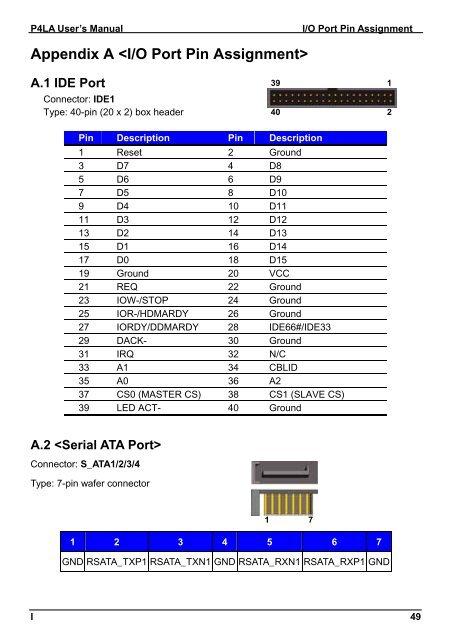
Appendix A <br />
A.1 IDE Port<br />
Connector: IDE1<br />
Type: 40-pin (20 x 2) box header<br />
39<br />
40<br />
1<br />
2<br />
Pin Description Pin Description<br />
1 Reset 2 Ground<br />
3 D7 4 D8<br />
5 D6 6 D9<br />
7 D5 8 D10<br />
9 D4 10 D11<br />
11 D3 12 D12<br />
13 D2 14 D13<br />
15 D1 16 D14<br />
17 D0 18 D15<br />
19 Ground 20 VCC<br />
21 REQ 22 Ground<br />
23 IOW-/STOP 24 Ground<br />
25 IOR-/HDMARDY 26 Ground<br />
27 IORDY/DDMARDY 28 IDE66#/IDE33<br />
29 DACK- 30 Ground<br />
31 IRQ 32 N/C<br />
33 A1 34 CBLID<br />
35 A0 36 A2<br />
37 CS0 (MASTER CS) 38 CS1 (SLAVE CS)<br />
39 LED ACT- 40 Ground<br />
A.2 <br />
Connector: S_ATA1/2/3/4<br />
Type: 7-pin wafer connector<br />
1 7<br />
1 2 3 4 5 6 7<br />
GND RSATA_TXP1 RSATA_TXN1 GND RSATA_RXN1 RSATA_RXP1 GND<br />
I 49