P. Yuan, et al., "Geiger-mode LADAR cameras" - Spectrolab
P. Yuan, et al., "Geiger-mode LADAR cameras" - Spectrolab
P. Yuan, et al., "Geiger-mode LADAR cameras" - Spectrolab

Create successful ePaper yourself
Turn your PDF publications into a flip-book with our unique Google optimized e-Paper software.
<strong>Geiger</strong>-<strong>mode</strong> <strong>LADAR</strong> cameras<br />
Ping <strong>Yuan</strong> * , Rengarajan Sudharsanan, Xiaogang Bai, Joseph Boisvert, Paul McDon<strong>al</strong>d, and<br />
Eduardo Labios<br />
<strong>Spectrolab</strong> Inc., a Boeing Company, 12500 Gladstone Ave., Sylmar, CA, USA 91342<br />
Bryan Morris, John P Nicholson, Gary M Stuart, and Harrison Danny<br />
Boeing DES, 4411 The 25 Way NE # 350, Albuquerque, NM 87109<br />
Stephen Van Duyne, Greg Pauls, and Stephen Ga<strong>al</strong>ema<br />
Black Forest Engineering, LLC, 1879 Austin Bluffs Parkway, Colorado Springs, CO 80918<br />
ABSTRACT<br />
The performance of <strong>Geiger</strong>-<strong>mode</strong> LAser D<strong>et</strong>ection and Ranging (<strong>LADAR</strong>) cameras is primarily defined by individu<strong>al</strong><br />
pixel attributes, such as dark count rate (DCR), photon d<strong>et</strong>ection efficiency (PDE), jitter, and crosst<strong>al</strong>k. However, for the<br />
expanding <strong>LADAR</strong> imaging applications, other factors, such as image uniformity, component tolerance,<br />
manufacturability, reliability, and operation<strong>al</strong> features, have to be considered. Recently we have developed new 32x32<br />
and 32x128 Read-Out Integrated Circuits (ROIC) for <strong>LADAR</strong> applications. With multiple filter and absorber structures,<br />
the 50-μm-pitch arrays demonstrate pixel crosst<strong>al</strong>k less than 100 ppm level, while maintaining a PDE greater than 40%<br />
at 4 V overbias. Besides the improved epitaxi<strong>al</strong> and process uniformity of the APD arrays, the new ROICs implement a<br />
Non-uniform Bias (NUB) circuit providing 4-bit bias voltage tunability over a 2.5 V range to individu<strong>al</strong>ly bias each<br />
pixel. All these features greatly increase the performance uniformity of the <strong>LADAR</strong> camera. Cameras based on these<br />
ROICs were integrated with a data acquisition system developed by Boeing DES. The 32x32 version has a range gate of<br />
up to 7 μs and can cover a range window of about 1 km with 14-bit and 0.5 ns timing resolution. The 32x128 camera can<br />
be operated at a frame rate of up to 20 kHz with 0.3 ns and 14-bit time resolution through a full CameraLink. The<br />
performance of the 32x32 <strong>LADAR</strong> camera has been demonstrated in a series of field tests on various vehicles.<br />
1. INTRODUCTION AND BACKGROUND<br />
The recent progress in the short wavelength infrared region (SWIR) three-dimension imaging provides an important<br />
solution for foliage pen<strong>et</strong>ration, camouflage imaging, and aeri<strong>al</strong> mapping in battlefield intelligence and Earth survey. Its<br />
airborne applications, which make the most potenti<strong>al</strong> mark<strong>et</strong> for this technology, have posted a series of ch<strong>al</strong>lenges to<br />
the camera. Because the laser and its service system take most of the size, weight, and power (SWAP) of a <strong>LADAR</strong><br />
system, it is critic<strong>al</strong> to maximize the camera sensitivity to reduce the laser power requirement in order to enhance the<br />
ranging distance and reduce the SWAP of the whole system. InP-based single-photon counting GM-APDs fit perfectly to<br />
this requirement. <strong>Geiger</strong>-<strong>mode</strong> av<strong>al</strong>anche photodiode foc<strong>al</strong> plane arrays (GM-FPAs) have been reported by both MIT<br />
Lincoln Laboratory 1 and Boeing <strong>Spectrolab</strong> 2 for SWIR applications. Due to the availability of high power emitters,<br />
most of the effort to date has been focused on photodiodes operating at 1.06 µm. Important figures of merits for GM-<br />
APDs include dark count rate (DCR) and photon d<strong>et</strong>ection efficiency (PDE) which tog<strong>et</strong>her establish the upper limit of<br />
the sign<strong>al</strong>-to-noise ratio for the entire sensor system. For active 3-D imaging, sensor’s FPA timing jitter and crosst<strong>al</strong>k are<br />
<strong>al</strong>so critic<strong>al</strong> because the jitter s<strong>et</strong>s the upper limit of range resolution while the latter greatly influences the spati<strong>al</strong><br />
resolution. Frame rate limits the sensor update time which is <strong>al</strong>so a critic<strong>al</strong> performance param<strong>et</strong>er in airborne<br />
applications. Since it is primarily d<strong>et</strong>ermined by the data process and download rate, the GM-APD afterpulsing, or<br />
tempor<strong>al</strong> crosst<strong>al</strong>k b<strong>et</strong>ween range gates, is norm<strong>al</strong>ly not a great concern in imaging applications as long as it is no less<br />
than 100 kHz. Other important param<strong>et</strong>ers include weight, power, and volume. Because most of the power consumed in<br />
a <strong>LADAR</strong> camera is by the thermoelectric coolers (TEC), a higher APD operation temperature is <strong>al</strong>ways welcome to<br />
airborne applications.<br />
* Email: ping.yuan@boeing.com; Tel: 818 898 7578; Fax : 818 838 7474.<br />
Laser Radar Technology and Applications XVI, edited by Monte D. Turner, Gary W. Kamerman,<br />
Proc. of SPIE Vol. 8037, 803712 · © 2011 SPIE · CCC code: 0277-786X/11/$18 · doi: 10.1117/12.884346<br />
Proc. of SPIE Vol. 8037 803712-1<br />
Downloaded from SPIE Digit<strong>al</strong> Library on 27 Oct 2011 to 130.76.64.116. Terms of Use: http://spiedl.org/terms
<strong>Spectrolab</strong> and Black Forest Engineering have been working under DARPA Elusive Surface Targ<strong>et</strong> Engagement<br />
Technology program to advance the performance of both the av<strong>al</strong>anche photodiode d<strong>et</strong>ector and ROIC arrays that<br />
tog<strong>et</strong>her comprise an FPA. Black Forest Engineering has designed a new 32x32 ROIC with enhanced capabilities that<br />
include: a non-uniform bias (NUB) correction that can be applied to individu<strong>al</strong> pixels across the array; and a modified<br />
pixel input circuit that effectively removes high dark current (shorted) APD pixels from the array to reduce the over<strong>al</strong>l<br />
current draw that would otherwise cause an FPA to fail. <strong>Spectrolab</strong> has introduced a feature to the APD d<strong>et</strong>ector array<br />
that reduces the optic<strong>al</strong> crosst<strong>al</strong>k b<strong>et</strong>ween pixels to
All these param<strong>et</strong>ers mentioned above must be optimized for the optim<strong>al</strong> sensor performance. In practice these<br />
param<strong>et</strong>ers are not decoupled and often trade off against one another. A robust FPA read out integrated circuit (ROIC)<br />
can improve sensor performance by mitigating APD deficiencies. However, an FPA design is fundament<strong>al</strong>ly limited by<br />
d<strong>et</strong>ector performance. Table 1 lists the most important FPA figures of merit that impact single photon counting sensor<br />
systems.<br />
2. GM-APD FPA FUNDAMENTALS<br />
In <strong>Geiger</strong>-<strong>mode</strong> operation the av<strong>al</strong>anche photodiodes are biased above the breakdown voltage, ~ 2-4 V, for a short period<br />
of time during which the sensor is active. If a photon in the sensitive spectrum f<strong>al</strong>ls on the d<strong>et</strong>ector pixel in this period, it<br />
has a probability to be absorbed and multiplied in the GM-APD such that the amplitude of the result pulse is large<br />
enough to be converted into a digit<strong>al</strong> pulse that can be registered by the following readout circuit. This probability is a<br />
figure of merit c<strong>al</strong>led photon d<strong>et</strong>ection efficiency (PDE). Due to various carrier generation mechanisms in GM-APDs,<br />
there is still some probability for the pixels to generate some output pulses even without any incident photons. This<br />
probability is characterized by dark count rate (DCR) and it represents the noise of GM-APD arrays. Typic<strong>al</strong>ly DCR<br />
increases with overbias and operating temperature. Because a higher overbias <strong>al</strong>so yields a b<strong>et</strong>ter PDE, for a b<strong>et</strong>ter<br />
sign<strong>al</strong>-to-noise ratio, the trade-off b<strong>et</strong>ween PDE and DCR has to be carefully considered in the device operation point<br />
selection. Figure 1 d<strong>et</strong>ails the gener<strong>al</strong> concepts of <strong>Geiger</strong>-<strong>mode</strong> operation.<br />
n-InGaAs<br />
n-InP<br />
InGaAs i-InGaAs<br />
or InGaAsP<br />
InGaAsP Graded layer<br />
N-InP Charge layer<br />
InGaAs(P)Absorber<br />
h<br />
e<br />
InP Multiplier<br />
Gain = ∞<br />
E<br />
i-<br />
InP Multiplier<br />
P-<br />
-InP Buffer 2<br />
P-<br />
InP Buffer 1<br />
InP Substrate<br />
hν<br />
P Substrate<br />
Figure 2.<br />
1.06 µm GM-APD device design and resultant electric field profile during operation.<br />
Figure 2 shows the InGaAsP/InP GM-APD separate absorption and gain and multiplication (SAGM) device structure for<br />
1.06 µm operation. The multiplication layer and silicon doped charge layer are both formed with InP. An InGaAsP<br />
<strong>al</strong>loy is used in the absorption layer for 1.06-µm photons. The right panel shows the electric field profile at operation in<br />
this device structure. With a carefully controlled charge layer, the electric filed in the multiplier is high for appreciable<br />
av<strong>al</strong>anche gain and it is low across the absorption layer to prevent tunneling of carrier so that the DCR is low in these<br />
Proc. of SPIE Vol. 8037 803712-3<br />
Downloaded from SPIE Digit<strong>al</strong> Library on 27 Oct 2011 to 130.76.64.116. Terms of Use: http://spiedl.org/terms
devices. The top N + InGaAs layer is used as a contact layer. The nomin<strong>al</strong> thickness the InGaAsP absorption layer is 1.5<br />
µm for good quantum efficiency. The device growth and characterization d<strong>et</strong>ails have been described in previous<br />
literatures 2 .<br />
3. SINGLE DEVICE PERFORMANCE<br />
As described earlier 2 , single element mesa devices with different mesa diam<strong>et</strong>ers, from 20 µm to 200 µm, are fabricated<br />
to ev<strong>al</strong>uate the qu<strong>al</strong>ity of epitaxi<strong>al</strong> wafers. Initi<strong>al</strong> I-V testing is done at room temperature to d<strong>et</strong>ermine the breakdown<br />
voltage, punch through voltage, and leakage current. The device optic<strong>al</strong> gain and responsivity were measured by<br />
illuminating with a 1.06 µm wavelength laser. The left panel of Figure 1 shows the dark current and gain versus bias<br />
characteristics of a 200 µm diam<strong>et</strong>er device. The bulk current density referred to unity gain is a typic<strong>al</strong> figure of merit<br />
for APDs and in this case J D (M=1)=630 nA/cm 2 . The most important figure of merits of GM APDs are DCR and PDE,<br />
and tog<strong>et</strong>her they define the sign<strong>al</strong>-to-noise ratio of the whole photon counting system. Because both increase with the<br />
overbias, it is critic<strong>al</strong> to trade off b<strong>et</strong>ween them in operation. The device optimization principles and strategies have been<br />
reported previously by Lincoln Laboratory 3 and <strong>Spectrolab</strong> 4 Figure 3 plots the PDE against DCR of three 25-μm array<br />
pixels on a 32x128 GM APD array under different overbiases and 243K. Grown on p-type InP substrates, the devices<br />
can achieve 40% PDE with 3~4 kHz DCR at the operation temperature.<br />
10809-9-F15(25 um pixel) 243K<br />
60.00%<br />
50.00%<br />
40.00%<br />
SPDE<br />
30.00%<br />
20.00%<br />
10.00%<br />
Figure 3.<br />
0.00%<br />
1.00E+02 1.00E+03 1.00E+04<br />
Dark cou nt rate (Hz )<br />
PDE as function of DCR of three typic<strong>al</strong> <strong>Spectrolab</strong> 25-µm diam<strong>et</strong>er <strong>Geiger</strong>-<strong>mode</strong> APD<br />
pixels of a 32x128 array. The data is measured at various overbias points and 243 K.<br />
4. SPECTROLAB 32X128 <strong>LADAR</strong> SENSOR CHIP ASSEMBLY<br />
With extensive capacities in MOVPE epitaxy, wafer process, and module packaging, <strong>Spectrolab</strong> vertic<strong>al</strong>ly integrated the<br />
<strong>LADAR</strong> camera manufacturing in house. After the d<strong>et</strong>ector array fabrication, Indium bumps were evaporated on to the<br />
array pixels. The d<strong>et</strong>ector array with indium bumps was integrated with a 32x128 ROIC designed by Black Forest<br />
Engineering by flip-chip bonding. A GaP microlens array of the same format was attached to the foc<strong>al</strong> plane array for a<br />
b<strong>et</strong>ter fill factor after this flip-chip process. As shown in Figure 4, the foc<strong>al</strong> plan array (FPA) was mounted on to a TE<br />
cooler and an interposer soldered in a 160-pin grid array package. Later, the package was herm<strong>et</strong>ic<strong>al</strong>ly se<strong>al</strong>ed with an<br />
AR-coated sapphire window into a sensor chip assembly (SCA).<br />
Proc. of SPIE Vol. 8037 803712-4<br />
Downloaded from SPIE Digit<strong>al</strong> Library on 27 Oct 2011 to 130.76.64.116. Terms of Use: http://spiedl.org/terms
Sapphire Window<br />
Be ze l<br />
AD590<br />
Temp sensor<br />
80 % A r<br />
20% He<br />
Kovar Housing<br />
AIN Interposer<br />
APD /CM OS<br />
RMT Ltd<br />
2MC04-039-05<br />
2-Stage TEC<br />
Alumina 69 PGA<br />
CuW H ea t sink<br />
Figure 4.<br />
The crosssection and top view of a <strong>Spectrolab</strong> 32x128 sensor chip assembly. The interposer<br />
for two FPAs are shown in lower right corner.<br />
1800<br />
1600<br />
1400<br />
1200<br />
1000<br />
800<br />
600<br />
400<br />
200<br />
0<br />
77.5 77.75 78 78.25 78.5 78.75 79 79.25 79.5 79.75 80<br />
Figure 5<br />
The Vbr map of an 32x128 GM APD array, in which each color represents a ¼ V range. The<br />
histogram of the Vbr of the 4096 pixels is illustrated in the bottom. The standard deviation of<br />
Vbr is about 0.14 V, and 99.3% of the pixels break down within 1V range.<br />
Proc. of SPIE Vol. 8037 803712-5<br />
Downloaded from SPIE Digit<strong>al</strong> Library on 27 Oct 2011 to 130.76.64.116. Terms of Use: http://spiedl.org/terms
Based on the device structure shown in Figure 2, the common anode is biased with a single negative voltage, while the<br />
pixels are applied a positive pulse uniformly in the d<strong>et</strong>ection gate. Due to the epitaxi<strong>al</strong> non-uniformity, norm<strong>al</strong>ly there is<br />
a breakdown voltage (Vbr) variation across the array. Under this bias scheme, the overbias to each pixel will vary with<br />
the breakdown voltage and result in non-uniformity in DCR and PDE. In order to achieve uniform performance, it is<br />
critic<strong>al</strong> to minimize the Vbr variation across the array. Figure 5 shows the Vbr map of an 32x128 GM APD array, in<br />
which each color represents a ¼ V range. The histogram of the Vbr of the 4096 pixels is illustrated in the bottom. The<br />
standard deviation of Vbr is about 0.14 V, and 99.3% of the pixels break down within 1V range.<br />
The DCR map of a 32x128 SCA operated at 242K and a frame rate of 12.5 kHz is shown in Figure 6. With applying the<br />
Non-uniform Bias (NUB) correction implemented in the ROIC, a uniform turn-on of the whole array was achieved. As<br />
shown in the bottom DCR histogram, the mean DCR is at 5.3 kHz, and more than 88% pixels have a DCR less than 10<br />
kHz.<br />
Figure 6.<br />
The DCR map of a 32x128 SCA operated at 242K and a frame rate of 12.5 kHz.<br />
Because the GM APDs are biased beyond the breakdown voltage and they are extremely sensitive to single photon level<br />
in the d<strong>et</strong>ection gate, any secondary emission from an av<strong>al</strong>anche event in an array can propagate to the neighbor pixels<br />
and trigger f<strong>al</strong>se d<strong>et</strong>ections. If this crosst<strong>al</strong>k probability is not well controlled, the chain reaction can turn on the whole<br />
array with a single input photon and severely degrade the <strong>LADAR</strong> image qu<strong>al</strong>ity. As the pixel pitch reduced from 100<br />
μm of the previously reported 32x32 GM APD arrays to 50 μm, the crosst<strong>al</strong>k is an even greater concern. Sever<strong>al</strong> layers<br />
of propri<strong>et</strong>ary isolation schemes were employed in the 32x128 array device design and process. As shown in Figure 7,<br />
the 50 μm pitch arrays demonstrated a crosst<strong>al</strong>k level about 60 ppm under the operation condition, which is about one<br />
order of magnitude less than that of the 100 μm pitch 32x32 arrays we reported before 5 .<br />
Proc. of SPIE Vol. 8037 803712-6<br />
Downloaded from SPIE Digit<strong>al</strong> Library on 27 Oct 2011 to 130.76.64.116. Terms of Use: http://spiedl.org/terms
1<br />
1.4<br />
2<br />
Figure 7.<br />
The crosst<strong>al</strong>k probability as a function of the distance to the initiating pixel. The pixel<br />
distance used in the x-axis is illustrated in the inserted diagram.<br />
5. SPECTROLAB GEN-II 32X32 <strong>LADAR</strong> CAMERA<br />
With the support from DARPA, a 32x32 readout-integrated circuit (ROIC), BFE316, was designed in 180-nm CMOS<br />
technology by Black Forest Engineering (BFE). Many improvements were incorporated in this design based on our<br />
experience with the previous versions. They include: bad pixel protection, 4-bit APD array NUB correction, 7 μs gate<br />
width with 0.5 ns resolution, 435-ps whole sy<strong>et</strong>em jitter, negligible chirp, 14V max overbias, and 300 mW power<br />
consumption 5 .<br />
By connecting the d<strong>et</strong>ector to a high impedance element, the front end circuit provides immunity to shorted d<strong>et</strong>ectors,<br />
which norm<strong>al</strong>ly sparse in APD arrays, and thus greatly improves the manufacturability and stability of FPAs. As shown<br />
in Figure 5, APD arrays have natur<strong>al</strong> variations in breakdown voltage, which results in a performance variation across<br />
the array if it is biased under a uniform bias. By introducing a 4-bit 2.5V in-pixel programmable NUB adjustment, the<br />
result SCA can achieve much b<strong>et</strong>ter performance uniformity. Because the FPA is at the top of sever<strong>al</strong> stages of TECs,<br />
which consume most of the power in a <strong>LADAR</strong> camera, the nearly h<strong>al</strong>ved ROIC power consumption dramatic<strong>al</strong>ly<br />
reduced the camera power load and heatsink weight.<br />
Laser<br />
Trigger<br />
Gate<br />
delay<br />
Laser<br />
Pulse out<br />
Laser<br />
r<strong>et</strong>urn<br />
Arm<br />
Camera<br />
Trigger<br />
Gate on<br />
APD Fired.<br />
Timing bin<br />
latched<br />
Gate off.<br />
Unfired<br />
pixels fired<br />
Array scan<br />
and readout.<br />
Figure 8.<br />
The typic<strong>al</strong> <strong>LADAR</strong> camera operation timing sequence.<br />
Proc. of SPIE Vol. 8037 803712-7<br />
Downloaded from SPIE Digit<strong>al</strong> Library on 27 Oct 2011 to 130.76.64.116. Terms of Use: http://spiedl.org/terms
With the readout boards developed at Boeing DES, the Gen-II 32x32 <strong>LADAR</strong> camera was integrated with the SCA<br />
based on the BFE 316 ROIC. The typic<strong>al</strong> <strong>LADAR</strong> system operation timing sequence is illustrated in Figure 8. With a<br />
certain intern<strong>al</strong> delay, a laser pulse is fired after a trigger to the laser. The range information is extracted from the flight<br />
time of the r<strong>et</strong>urn sign<strong>al</strong> reflected from targ<strong>et</strong>. With GM APDs, the r<strong>et</strong>urn sign<strong>al</strong> can be effectively d<strong>et</strong>ected at the single<br />
photon level. This sensitivity greatly extends the <strong>LADAR</strong> system range, reduces the laser power requirements and the<br />
lens size, and minimizes the SWAP of the over<strong>al</strong>l system. On the camera side, the ROIC will be armed after a certain<br />
delay to the camera trigger. Then, the overbias to the APD array is applied and the d<strong>et</strong>ection gate is turned on. In<br />
<strong>Spectrolab</strong> Gen-II 32x32 <strong>LADAR</strong> camera, this gate can be kept on for about 7 μs, which provides a range window of<br />
about 1 km long. Addition<strong>al</strong> range coverage can be re<strong>al</strong>ized by inserting a delay b<strong>et</strong>ween the laser pulse and gate turn-on<br />
and shifting the range window until reaching the maximum range <strong>al</strong>lowed by the laser power and the array sensitivity.<br />
With a proper delay, the laser sign<strong>al</strong> will f<strong>al</strong>l in the d<strong>et</strong>ection gate and fire pixels in the array. The following circuits of<br />
the fired pixels will latch the timing of the d<strong>et</strong>ection. At the end of the gate, the whole array will be scanned and the<br />
timing information will be read out.<br />
Figure 9<br />
The top graph shows the tempor<strong>al</strong> histogram of a single laser pulse d<strong>et</strong>ected by a <strong>Spectrolab</strong><br />
Gen-II 32x32 <strong>LADAR</strong> camera. The over<strong>al</strong>l system RMS jitter is about 435 ps. The bottom<br />
panel shows a series of sign<strong>al</strong>s d<strong>et</strong>ected from laser pulses delayed by 500 ns from each other.<br />
The ranging resolution of a <strong>LADAR</strong> camera is d<strong>et</strong>ermined by its over<strong>al</strong>l jitter and chirp performance. The tempor<strong>al</strong><br />
histogram of our Gen-II 32x32 camera to a synchronized 90 ps laser pulse is shown in the top panel of Figure 9. The bin<br />
size is 500 ps, and the laser pulse width is included in this measurement. By c<strong>al</strong>culating the standard deviation of this<br />
Proc. of SPIE Vol. 8037 803712-8<br />
Downloaded from SPIE Digit<strong>al</strong> Library on 27 Oct 2011 to 130.76.64.116. Terms of Use: http://spiedl.org/terms
tempor<strong>al</strong> distribution, we can g<strong>et</strong> the over<strong>al</strong>l system RMS jitter of 435 ps, which includes the laser pulse width and jitters<br />
in the trigger loop, APDs, ROIC, and readout boards. With a new clock design, the chirp in this camera is negligible. As<br />
shown in the bottom panel of Figure 9, by increasing the delay of a laser pulse 500 ns each time, we have got a series of<br />
evenly spaced sign<strong>al</strong>s in the d<strong>et</strong>ection gate.<br />
Figure 10.<br />
Photon counting <strong>LADAR</strong> system integrated with the <strong>Spectrolab</strong> Gen-II <strong>LADAR</strong> camera by<br />
Boeing DES.<br />
Figure 10 shows the <strong>LADAR</strong> system integrated with the <strong>Spectrolab</strong> Gen-II camera by Boeing DES. The tot<strong>al</strong> weight is<br />
less than 20 lbs with the lens and scanning mechanics. The size is 7.5”x22”x6”, and the power consumption is less than<br />
325W. With data reduction from hundreds of MB/s raw data to about 20 MB/s, this compact <strong>LADAR</strong> system gives the<br />
user rapid 3D imagery to access the mapped area quickly and accurately. This system has been demonstrated on various<br />
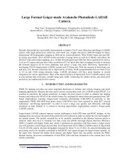
aeri<strong>al</strong> platforms. Figure 11 shows the 3D images of forested areas and the Rio Grande near Albuquerque, NM generated<br />
by this <strong>LADAR</strong> system mounted on a hot air b<strong>al</strong>loon.<br />
+/- 7° scan<br />
@ 2Hz<br />
11.5 mph<br />
@ 1125 ft<br />
AGL<br />
Height<br />
H i ht<br />
Figure 11<br />
3D images of forested areas and the Rio Grande near Albuquerque, NM generated by a<br />
compact Boeing DES <strong>LADAR</strong> system mounted on a hot air b<strong>al</strong>loon.<br />
Proc. of SPIE Vol. 8037 803712-9<br />
Downloaded from SPIE Digit<strong>al</strong> Library on 27 Oct 2011 to 130.76.64.116. Terms of Use: http://spiedl.org/terms
6. SUMMARY<br />
To answer the ch<strong>al</strong>lenges of SWIR <strong>LADAR</strong> applications, <strong>Spectrolab</strong>, teamed with Boeing DES and Black Forest<br />
Engineering, has been developing 32x128 GM-APD SCA and Gen-II <strong>LADAR</strong> camera. <strong>LADAR</strong> SCA performance has<br />
been greatly improved due to the continuous effect in materi<strong>al</strong>s, device design. Black Forest Engineering has designed<br />
and tested a new 32x32 ROIC loaded with many new functions and improved performance. The integration effort at<br />
Boeing DES made the cameras convenient to operate and commerci<strong>al</strong>ly available. A compact <strong>LADAR</strong> system based on<br />
the new 32x32 camera was demonstrated on various platforms. With the 32x128 <strong>LADAR</strong> SCA developed under the<br />
DARPA program, the <strong>Spectrolab</strong>, Black Forest Engineering, and Boeing DES team, is developing the next generation<br />
GM APD 128x32 <strong>LADAR</strong> camera for SWIR applications.<br />
ACKNOWLEDGEMENTS<br />
We would like to acknowledge the inv<strong>al</strong>uable assistance provided by MIT Lincoln Laboratory over the last sever<strong>al</strong> years<br />
under various technology transfer programs. This effort has been funded under Boeing Whitespace program and<br />
DARPA Elusive Surface Targ<strong>et</strong> Engagement Technology contract HR0011-08-C-0020 under the direction of Dr. Monte<br />
Turner.<br />
REFERENCES<br />
1 K. A. McIntosh, <strong>et</strong> <strong>al</strong>., “Arrays of III-V semiconductor <strong>Geiger</strong>-<strong>mode</strong> av<strong>al</strong>anche photodiodes,” Lasers and Electro-<br />
Optics Soci<strong>et</strong>y, 2003. LEOS 2003. The 16th Annu<strong>al</strong> Me<strong>et</strong>ing of the IEEE. Volume 2, 686 (2003).<br />
2 R. Sudharsanan, <strong>et</strong> <strong>al</strong>., “Single photon counting <strong>Geiger</strong> Mode InGaAs(P)/InP av<strong>al</strong>anche photodiode arrays for 3D<br />
imaging,” Proc. SPIE 6950, 69500N (2008).<br />
3 S. Verghese, <strong>et</strong> <strong>al</strong>., “Arrays of InP-based Av<strong>al</strong>anche Photodiodes for Photon Counting,” IEEE J. Selected Topics in<br />
Quantum Electronics, 13, 870 (2007).<br />
4 P. <strong>Yuan</strong>, <strong>et</strong> <strong>al</strong>., “High-performance InP <strong>Geiger</strong>-<strong>mode</strong> SWIR av<strong>al</strong>anche photodiodes,”, SPIE Defense, Security, and<br />
Sensing, Advanced Photon Counting Techniques III. Proc. SPIE 7320, 73200P (2009).<br />
5 P. <strong>Yuan</strong>, <strong>et</strong> <strong>al</strong>., “32 x 32 <strong>Geiger</strong>-<strong>mode</strong> <strong>LADAR</strong> cameras,” SPIE Defense, Security, and Sensing, Laser Radar<br />
Technology and Applications XV. Proc. SPIE 7684, 76840C (2010).<br />
Proc. of SPIE Vol. 8037 803712-10<br />
Downloaded from SPIE Digit<strong>al</strong> Library on 27 Oct 2011 to 130.76.64.116. Terms of Use: http://spiedl.org/terms