OPA336, 2336, 4336: Single-Supply, microPower ... - SP-Elektroniikka
OPA336, 2336, 4336: Single-Supply, microPower ... - SP-Elektroniikka
OPA336, 2336, 4336: Single-Supply, microPower ... - SP-Elektroniikka

Create successful ePaper yourself
Turn your PDF publications into a flip-book with our unique Google optimized e-Paper software.
<strong>OPA336</strong> OPA<strong>2336</strong><br />
OPA<strong>4336</strong><br />
<strong>OPA336</strong><br />
OPA<strong>2336</strong><br />
OPA<strong>4336</strong><br />
SBOS068C – JANUARY 1997 – REVISED JANUARY 2005<br />
SINGLE-SUPPLY, <strong>microPower</strong><br />
CMOS OPERATIONAL AMPLIFIERS<br />
microAmplifier Series<br />
FEATURES<br />
● SINGLE-SUPPLY OPERATION<br />
● RAIL-TO-RAIL OUTPUT (within 3mV)<br />
● microPOWER: I Q = 20µA/Amplifier<br />
● microSIZE PACKAGES<br />
● LOW OFFSET VOLTAGE: 125µV max<br />
● <strong>SP</strong>ECIFIED FROM V S = 2.3V to 5.5V<br />
● SINGLE, DUAL, AND QUAD VERSIONS<br />
APPLICATIONS<br />
● BATTERY-POWERED INSTRUMENTS<br />
● PORTABLE DEVICES<br />
● HIGH-IMPEDANCE APPLICATIONS<br />
● PHOTODIODE PRE-AMPS<br />
● PRECISION INTEGRATORS<br />
● MEDICAL INSTRUMENTS<br />
● TEST EQUIPMENT<br />
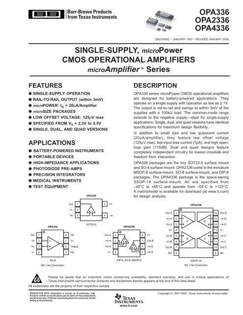
<strong>OPA336</strong><br />
DESCRIPTION<br />
<strong>OPA336</strong> series <strong>microPower</strong> CMOS operational amplifiers<br />
are designed for battery-powered applications. They<br />
operate on a single supply with operation as low as 2.1V.<br />
The output is rail-to-rail and swings to within 3mV of the<br />
supplies with a 100kΩ load. The common-mode range<br />
extends to the negative supply—ideal for single-supply<br />
applications. <strong>Single</strong>, dual, and quad versions have identical<br />
specifications for maximum design flexibility.<br />
In addition to small size and low quiescent current<br />
(20µA/amplifier), they feature low offset voltage<br />
(125µV max), low input bias current (1pA), and high openloop<br />
gain (115dB). Dual and quad designs feature<br />
completely independent circuitry for lowest crosstalk and<br />
freedom from interaction.<br />
<strong>OPA336</strong> packages are the tiny SOT23-5 surface mount<br />
and SO-8 surface-mount. OPA<strong>2336</strong> come in the miniature<br />
MSOP-8 surface-mount, SO-8 surface-mount, and DIP-8<br />
packages. The OPA<strong>4336</strong> package is the space-saving<br />
SSOP-16 surface-mount. All are specified from<br />
–40°C to +85°C and operate from –55°C to +125°C.<br />
A macromodel is available for download (at www.ti.com)<br />
for design analysis.<br />
Out<br />
1<br />
5<br />
V+<br />
OPA<strong>4336</strong><br />
<strong>OPA336</strong><br />
V–<br />
+In<br />
2<br />
3<br />
SOT23-5<br />
4<br />
–In<br />
OPA<strong>2336</strong><br />
Out A<br />
–In A<br />
+In A<br />
V+<br />
1<br />
2<br />
3<br />
4<br />
A<br />
D<br />
16<br />
15<br />
14<br />
13<br />
Out D<br />
–In D<br />
+In D<br />
V–<br />
NC<br />
–In<br />
+In<br />
1<br />
2<br />
3<br />
8<br />
7<br />
6<br />
NC<br />
V+<br />
Output<br />
Out A<br />
–In A<br />
+In A<br />
1<br />
2<br />
3<br />
A<br />
B<br />
8<br />
7<br />
6<br />
V+<br />
Out B<br />
–In B<br />
+In B<br />
–In B<br />
Out B<br />
5<br />
6<br />
7<br />
B<br />
C<br />
12<br />
11<br />
10<br />
+In C<br />
–In C<br />
Out C<br />
V–<br />
4<br />
5<br />
NC<br />
V–<br />
4<br />
5<br />
+In B<br />
NC<br />
8<br />
9<br />
NC<br />
SO-8<br />
NC = No Connection<br />
DIP-8, SO-8, MSOP-8<br />
SSOP-16<br />
NC = No Connection<br />
Please be aware that an important notice concerning availability, standard warranty, and use in critical applications of<br />
Texas Instruments semiconductor products and disclaimers thereto appears at the end of this data sheet.<br />
All trademarks are the property of their respective owners.<br />
PRODUCTION DATA information is current as of publication date.<br />
Products conform to specifications per the terms of Texas Instruments<br />
standard warranty. Production processing does not necessarily include<br />
testing of all parameters.<br />
www.ti.com<br />
Copyright © 1997-2005, Texas Instruments Incorporated
PACKAGE/ORDERING INFORMATION (1)<br />
PACKAGE<br />
DRAWING<br />
PACKAGE<br />
PRODUCT PACKAGE-LEAD DESIGNATOR MARKING<br />
<strong>Single</strong><br />
<strong>OPA336</strong>N SOT23-5 DBV A36 (2)<br />
<strong>OPA336</strong>NA SOT23-5 DBV A36 (2)<br />
<strong>OPA336</strong>NJ SOT23-5 DBV J36<br />
<strong>OPA336</strong>U SO-8 Surface-Mount D <strong>OPA336</strong>U<br />
<strong>OPA336</strong>UA SO-8 Surface-Mount D <strong>OPA336</strong>UA<br />
<strong>OPA336</strong>UJ SO-8 Surface-Mount D <strong>OPA336</strong>UJ<br />
Dual<br />
OPA<strong>2336</strong>E MSOP-8 Surface-Mount DGK B36 (2)<br />
OPA<strong>2336</strong>EA MSOP-8 Surface-Mount DGK B36 (2)<br />
OPA<strong>2336</strong>P DIP-8 P OPA<strong>2336</strong>P<br />
OPA<strong>2336</strong>PA DIP-8 P OPA<strong>2336</strong>PA<br />
OPA<strong>2336</strong>U SO-8 Surface-Mount D OPA<strong>2336</strong>U<br />
OPA<strong>2336</strong>UA SO-8 Surface-Mount D OPA<strong>2336</strong>UA<br />
Quad<br />
OPA<strong>4336</strong>EA SSOP-16 Surface-Mount DBQ OPA<strong>4336</strong>EA<br />
NOTES: (1) For the most current package and ordering information, see the package option addendum at the end of this data sheet. (2) Grade will be marked on<br />
the Reel.<br />
ABSOLUTE MAXIMUM RATINGS (1)<br />
<strong>Supply</strong> Voltage ................................................................................... 7.5V<br />
Signal Input Terminals, Voltage (2) ..................... (V–) –0.3V to (V+) +0.3V<br />
Current (2) .................................................... 10mA<br />
Output Short-Circuit (3) .............................................................. Continuous<br />
Operating Temperature ..................................................–55°C to +125°C<br />
Storage Temperature ..................................................... –55°C to +125°C<br />
Junction Temperature ...................................................................... 150°C<br />
Lead Temperature (soldering, 10s) ................................................. 300°C<br />
ESD Rating:<br />
Charged Device Model, <strong>OPA336</strong> NJ and UJ only (CDM) (4) ....... 1000V<br />
Human Body Model (HBM) (4) ......................................................... 500V<br />
Machine Model (MM) (4) .................................................................. 100V<br />
NOTES: (1) Stresses above these ratings may cause permanent damage.<br />
Exposure to absolute maximum conditions for extended periods may<br />
degrade device reliability. These are stress ratings only. Functional operation<br />
of the device at these conditions, or beyond the specified operating<br />
conditions, is not implied. (2) Input terminals are diode-clamped to the power<br />
supply rails. Input signals that can swing more than 0.3V beyond the supply<br />
rails should be current-limited to 10mA or less. (3) Short-circuit to ground,<br />
one amplifier per package. (4) <strong>OPA336</strong> NJ and UJ have been tested to CDM<br />
of 1000V. All other previous package versions have been tested using HBM<br />
and MM. Results are shown.<br />
ELECTROSTATIC<br />
DISCHARGE SENSITIVITY<br />
This integrated circuit can be damaged by ESD. Texas<br />
Instruments recommends that all integrated circuits be handled<br />
with appropriate precautions. Failure to observe proper handling<br />
and installation procedures can cause damage.<br />
ESD damage can range from subtle performance degradation<br />
to complete device failure. Precision integrated circuits<br />
may be more susceptible to damage because very small<br />
parametric changes could cause the device not to meet its<br />
published specifications.<br />
2<br />
www.ti.com<br />
<strong>OPA336</strong>, <strong>2336</strong>, <strong>4336</strong><br />
SBOS068C
ELECTRICAL CHARACTERISTICS: V S = 2.3V to 5.5V<br />
Boldface limits apply over the specified temperature range, T A = –40°C to +85°C.<br />
At T A = +25°C, V S = +5V, and R L = 25kΩ connected to V S /2, unless otherwise noted.<br />
<strong>OPA336</strong>NA, UA<br />
<strong>OPA336</strong>N, U OPA<strong>2336</strong>EA, PA, UA<br />
OPA<strong>2336</strong>E, P, U OPA<strong>4336</strong>EA <strong>OPA336</strong>NJ, UJ<br />
PARAMETER CONDITION MIN TYP (1) MAX MIN TYP MAX MIN TYP MAX UNITS<br />
OFFSET VOLTAGE<br />
Input Offset Voltage V OS ±60 ±125 ✻ ±500 ±500 ±2500 µV<br />
vs Temperature dV OS /dT ±1.5 ✱ ✱ µV/°C<br />
vs Power <strong>Supply</strong> PSRR V S = 2.3V to 5.5V 25 100 ✻ ✻ ✻ ✻ ✻ µV/V<br />
Over Temperature V S = 2.3V to 5.5V 130 ✱ ✱ ✱ µV/V<br />
Channel Separation, dc 0.1 ✻ ✻ µV/V<br />
INPUT BIAS CURRENT<br />
Input Bias Current I B ±1 ±10 ✻ ✻ ✻ ✻ pA<br />
Over Temperature ±60 ✱ ✱ pA<br />
Input Offset Current I OS ±1 ±10 ✻ ✻ ✻ ✻ pA<br />
NOISE<br />
Input Voltage Noise, f = 0.1 to 10Hz 3 ✻ ✻ µVp-p<br />
Input Voltage Noise Density, f = 1kHz e n 40 ✻ ✻ nV/√Hz<br />
Current Noise Density, f = 1kHz i n 30 ✻ ✻ fA/√Hz<br />
INPUT VOLTAGE RANGE<br />
Common-Mode Voltage Range V CM –0.2 (V+) –1 ✻ ✻ ✻ ✻ V<br />
Common-Mode Rejection Ratio CMRR –0.2V < V CM < (V+) –1V 80 90 76 86 76 86 dB<br />
Over Temperature –0.2V < V CM < (V+) –1V 76 74 74 dB<br />
INPUT IMPEDANCE<br />
Differential 10 13 || 2 ✻ ✻ Ω || pF<br />
Common-Mode 10 13 || 4 ✻ ✻ Ω || pF<br />
OPEN-LOOP GAIN<br />
Open-Loop Voltage Gain A OL R L = 25kΩ, 100mV < V O < (V+) – 100mV 100 115 90 ✻ 90 ✻ dB<br />
Over Temperature R L = 25kΩ, 100mV < V O < (V+) – 100mV 100 90 90 dB<br />
R L = 5kΩ, 500mV < V O < (V+) – 500mV 90 106 ✻ ✻ ✻ ✻ dB<br />
Over Temperature R L = 5kΩ, 500mV < V O < (V+) – 500mV 90 ✱ ✱ dB<br />
FREQUENCY RE<strong>SP</strong>ONSE<br />
Gain-Bandwidth Product GBW V S = 5V, G = 1 100 ✻ ✻ kHz<br />
Slew Rate SR V S = 5V, G = 1 0.03 ✻ ✻ V/µs<br />
Overload Recovery Time V IN • G = V S 100 ✻ ✻ µs<br />
OUTPUT<br />
Voltage Output Swing from Rail (2) R L = 100kΩ, A OL ≥ 70dB 3 ✻ ✻ mV<br />
R L = 25kΩ, A OL ≥ 90dB 20 100 ✻ ✻ ✻ ✻ mV<br />
Over Temperature R L = 25kΩ, A OL ≥ 90dB 100 ✱ ✱ mV<br />
R L = 5kΩ, A OL ≥ 90dB 70 500 ✻ ✻ ✻ ✻ mV<br />
Over Temperature R L = 5kΩ, A OL ≥ 90dB 500 ✱ ✱ mV<br />
Short-Circuit Current I SC ±5 ✻ ✻ mA<br />
Capacitive Load Drive C LOAD See Text ✻ ✻ pF<br />
POWER SUPPLY<br />
Specified Voltage Range V S 2.3 5.5 ✻ ✻ ✻ ✻ V<br />
Minimum Operating Voltage 2.1 ✻ ✻ V<br />
Quiescent Current (per amplifier) I Q I O = 0 20 32 ✻ ✻ 23 38 µA<br />
Over Temperature I O = 0 36 ✱ 42 µA<br />
TEMPERATURE RANGE<br />
Specified Range –40 +85 ✻ ✻ ✻ ✻ °C<br />
Operating Range –55 +125 ✻ ✻ ✻ ✻ °C<br />
Storage Range –55 +125 ✻ ✻ ✻ ✻ °C<br />
Thermal Resistance<br />
θ JA<br />
SOT-23-5 Surface-Mount 200 ✻ ✻ °C/W<br />
MSOP-8 Surface-Mount 150 ✻ °C/W<br />
SO-8 Surface-Mount 150 ✻ ✻ °C/W<br />
DIP-8 100 ✻ °C/W<br />
SSOP-16 Surface-Mount 100 ✻ °C/W<br />
DIP-14 80 ✻ °C/W<br />
✻Specifications same as OPA<strong>2336</strong>E, P, U.<br />
NOTES: (1) V S = +5V. (2) Output voltage swings are measured between the output and positive and negative power-supply rails.<br />
<strong>OPA336</strong>, <strong>2336</strong>, <strong>4336</strong> 3<br />
SBOS068C<br />
www.ti.com
TYPICAL CHARACTERISTICS<br />
At T A = +25°C, V S = +5V, and R L = 25kΩ connected to V S /2, unless otherwise noted.<br />
Voltage Gain (dB)<br />
Quiescent Current (µA)<br />
Short-Circuit Current (mA)<br />
–I SC<br />
+I SC<br />
–I SC 2<br />
V S = +2.3V –I SC<br />
POWER-SUPPLY and COMMON-MODE<br />
OPEN-LOOP GAIN/PHASE vs FREQUENCY<br />
REJECTION RATIO vs FREQUENCY<br />
100<br />
80<br />
60<br />
100<br />
G<br />
0<br />
80<br />
–45<br />
60<br />
CMRR<br />
40<br />
–90<br />
PSRR<br />
Φ<br />
40<br />
20<br />
0<br />
–20<br />
–135<br />
–180<br />
20<br />
0<br />
1 10 100 1k 10k 100k 1M<br />
1 10 100 1k 10k 100k<br />
Frequency (Hz)<br />
Frequency (Hz)<br />
QUIESCENT CURRENT vs SUPPLY VOLTAGE<br />
QUIESCENT CURRENT vs TEMPERATURE<br />
30<br />
30<br />
Per Amplifier<br />
Per Amplifier<br />
25<br />
V S<br />
= +5V<br />
25<br />
20<br />
20<br />
15<br />
10<br />
V S<br />
= +2.3V<br />
15<br />
5<br />
10<br />
0<br />
2.0 2.5 3.0 3.5 4.0 4.5 5.0 5.5 6.0<br />
–75 –50 –25 0 25 50 75 100 125<br />
<strong>Supply</strong> Voltage (V)<br />
Temperature (°C)<br />
SHORT-CIRCUIT CURRENT vs SUPPLY VOLTAGE<br />
SHORT-CIRCUIT CURRENT vs TEMPERATURE<br />
±6<br />
8<br />
±5<br />
7<br />
V S = +5V<br />
6<br />
±4<br />
+I SC<br />
5<br />
±3<br />
4<br />
+I SC<br />
±2<br />
3<br />
±1<br />
1<br />
Phase (°)<br />
PSRR, CMRR (dB)<br />
Quiescent Current (µA)<br />
Short-Circuit Current (mA)<br />
0<br />
2.0 2.5 3.0 3.5 4.0 4.5 5.0 5.5 6.0<br />
<strong>Supply</strong> Voltage (V)<br />
0<br />
–75 –50 –25 0 25 50 75 100 125<br />
Temperature (°C)<br />
4<br />
www.ti.com<br />
<strong>OPA336</strong>, <strong>2336</strong>, <strong>4336</strong><br />
SBOS068C
TYPICAL CHARACTERISTICS (Cont.)<br />
At T A = +25°C, V S = +5V, and R L = 25kΩ connected to V S /2, unless otherwise noted.<br />
1k<br />
INPUT VOLTAGE AND CURRENT NOISE<br />
<strong>SP</strong>ECTRAL DENSITY vs FREQUENCY<br />
1k<br />
150<br />
CHANNEL SEPARATION vs FREQUENCY<br />
Voltage Noise<br />
Voltage Noise (nV/√Hz)<br />
100<br />
10<br />
Current Noise<br />
100<br />
10<br />
Current Noise (fA/√Hz)<br />
Channel Separation (dB)<br />
140<br />
130<br />
120<br />
1<br />
1 10 100 1k 10k 100k<br />
Frequency (Hz)<br />
6<br />
MAXIMUM OUTPUT VOLTAGE vs FREQUENCY<br />
120<br />
A OL , CMRR, PSRR vs TEMPERATURE<br />
A OL<br />
PSRR<br />
Output Voltage (Vp-p)<br />
5<br />
4<br />
3<br />
2<br />
1<br />
V S = +2.3V<br />
V S = +5.5V<br />
0<br />
100 1k<br />
10k<br />
Frequency (Hz)<br />
100k<br />
Temperature (°C)<br />
Percent of Amplifiers (%)<br />
25<br />
20<br />
15<br />
10<br />
5<br />
Typical production<br />
distribution of<br />
packaged units.<br />
0.1%<br />
OFFSET VOLTAGE<br />
PRODUCTION DISTRIBUTION<br />
0.3% 0.2% 0.1%<br />
0<br />
–500<br />
–400<br />
–300<br />
–200<br />
–100<br />
A OL , CMRR, PSRR (dB)<br />
0<br />
100<br />
200<br />
300<br />
400<br />
500<br />
110<br />
100<br />
90<br />
80<br />
CMRR<br />
70<br />
–75 –50 –25 0 25 50 75 100 125<br />
Percent of Amplifiers (%)<br />
25<br />
20<br />
15<br />
10<br />
5<br />
OFFSET VOLTAGE DRIFT MAGNITUDE<br />
PRODUCTION DISTRIBUTION<br />
Typical production<br />
distribution of<br />
packaged units.<br />
0<br />
0.25<br />
0.5<br />
0.75<br />
1<br />
1.25<br />
1.5<br />
1.75<br />
2<br />
2.25<br />
2.5<br />
2.75<br />
3<br />
3.25<br />
3.5<br />
3.75<br />
4<br />
Dual and Quad devices, G = 1, all<br />
channels. Quad measured channel A<br />
to D or B to C—other combinations<br />
yield improved rejection.<br />
110<br />
100 1k 10k 100k<br />
Frequency (Hz)<br />
Offset Voltage (µV)<br />
Offset Voltage Drift (µV/°C)<br />
<strong>OPA336</strong>, <strong>2336</strong>, <strong>4336</strong> 5<br />
SBOS068C<br />
www.ti.com
TYPICAL CHARACTERISTICS (Cont.)<br />
At T A = +25°C, V S = +5V, and R L = 25kΩ connected to V S /2, unless otherwise noted.<br />
1k<br />
INPUT BIAS CURRENT vs TEMPERATURE<br />
4<br />
INPUT BIAS CURRENT<br />
vs INPUT COMMON-MODE VOLTAGE<br />
Input Bias Current (pA)<br />
100<br />
10<br />
1<br />
Input Bias Current (pA)<br />
3<br />
2<br />
1<br />
V S = +5V<br />
0.1<br />
–75 –50 –25 0 25 50 75 100 125<br />
Temperature (°C)<br />
0<br />
0 1 2 3 4 5<br />
Common-Mode Voltage (V)<br />
5<br />
OUTPUT VOLTAGE SWING vs OUTPUT CURRENT<br />
–2.5<br />
OUTPUT VOLTAGE SWING vs OUTPUT CURRENT<br />
V S = +5V<br />
V S = ±2.5V<br />
Output Voltage (V)<br />
4<br />
3<br />
2<br />
1<br />
Sourcing<br />
Current<br />
V S = +2.3V<br />
–55°C<br />
–55°C<br />
+125°C<br />
+25°C<br />
+125°C<br />
Output Voltage (V)<br />
–2.0<br />
–1.5<br />
–1.0<br />
–0.5<br />
Sinking<br />
Current<br />
–55°C<br />
+25°C<br />
+125°C<br />
+25°C<br />
0<br />
0 1 2 3 4 5 6 7 8<br />
Output Current (mA)<br />
0<br />
–0 –1 –2 –3 –4 –5 –6 –7 –8<br />
Output Current (mA)<br />
SMALL-SIGNAL STEP RE<strong>SP</strong>ONSE<br />
G = 1, C L = 200pF, V S = +5V<br />
LARGE-SIGNAL STEP RE<strong>SP</strong>ONSE<br />
G = 1, C L = 620pF, V S = +5V<br />
20mV/div<br />
500mV/div<br />
50µs/div<br />
200µs/div<br />
6<br />
www.ti.com<br />
<strong>OPA336</strong>, <strong>2336</strong>, <strong>4336</strong><br />
SBOS068C
APPLICATIONS INFORMATION<br />
<strong>OPA336</strong> series op amps are fabricated on a state-of-the-art<br />
0.6 micron CMOS process. They are unity-gain stable and<br />
suitable for a wide range of general-purpose applications.<br />
Power-supply pins should be bypassed with 0.01µF ceramic<br />
capacitors. <strong>OPA336</strong> series op amps are protected against<br />
reverse battery voltages.<br />
OPERATING VOLTAGE<br />
<strong>OPA336</strong> series op amps can operate from a +2.1V to +5.5V<br />
single supply with excellent performance. Most behavior<br />
remains unchanged throughout the full operating voltage<br />
range. Parameters which vary significantly with operating<br />
voltage are shown in the typical characteristics. <strong>OPA336</strong><br />
series op amps are fully specified for operation from +2.3V<br />
to +5.5V; a single limit applies over the supply range. In<br />
addition, many parameters are ensured over the specified<br />
temperature range, –40°C to +85°C.<br />
INPUT VOLTAGE<br />
The input common-mode range of <strong>OPA336</strong> series op amps<br />
extends from (V–) – 0.2V to (V+) – 1V. For normal<br />
operation, inputs should be limited to this range. The<br />
absolute maximum input voltage is 300mV beyond the<br />
supplies. Thus, inputs greater than the input<br />
common-mode range but less than maximum input voltage,<br />
while not valid, will not cause any damage to the op<br />
amp. Furthermore, the inputs may go beyond the power<br />
supplies without phase inversion, as shown in Figure 1,<br />
unlike some other op amps.<br />
6V<br />
V OUT<br />
Normally, input bias current is approximately 1pA. However,<br />
input voltages exceeding the power supplies can<br />
cause excessive current to flow in or out of the input pins.<br />
Momentary voltages greater than the power supply can be<br />
tolerated as long as the current on the input pins is limited<br />
to 10mA. This is easily accomplished with an input resistor,<br />
as shown in Figure 2.<br />
V IN<br />
I OVERLOAD<br />
10mA max<br />
5kΩ<br />
+5V<br />
OPAx336<br />
V OUT<br />
FIGURE 2. Input Current Protection for Voltages Exceeding<br />
the <strong>Supply</strong> Voltage.<br />
CAPACITIVE LOAD AND STABILITY<br />
<strong>OPA336</strong> series op amps can drive a wide range of capacitive<br />
loads. However, all op amps under certain conditions<br />
may become unstable. Op-amp configuration, gain, and<br />
load value are just a few of the factors to consider when<br />
determining stability.<br />
When properly configured, <strong>OPA336</strong> series op amps can<br />
drive approximately 10,000pF. An op amp in unity-gain<br />
configuration is the most vulnerable to capacitive load. The<br />
capacitive load reacts with the op amp’s output resistance,<br />
along with any additional load resistance, to create a pole in<br />
the response which degrades the phase margin. In unity gain,<br />
<strong>OPA336</strong> series op amps perform well with a pure capacitive<br />
load up to about 300pF. Increasing gain enhances the<br />
amplifier’s ability to drive loads beyond this level.<br />
One method of improving capacitive load drive in the<br />
unity-gain configuration is to insert a 50Ω to 100Ω resistor<br />
inside the feedback loop, as shown in Figure 3. This reduces<br />
ringing with large capacitive loads while maintaining DC<br />
0V<br />
V IN<br />
OPAx336<br />
R S<br />
100Ω<br />
V OUT<br />
C L<br />
R L<br />
FIGURE 1. No Phase Inversion with Inputs Greater than the<br />
Power-<strong>Supply</strong> Voltage.<br />
FIGURE 3. Series Resistor in Unity-Gain Configuration<br />
Improves Capacitive Load Drive.<br />
<strong>OPA336</strong>, <strong>2336</strong>, <strong>4336</strong> 7<br />
SBOS068C<br />
www.ti.com
accuracy. For example, with R L = 25kΩ, <strong>OPA336</strong> series op<br />
amps perform well with capacitive loads in excess of 1000pF,<br />
as shown in Figure 4. Without R S , capacitive load drive is<br />
typically 350pF for these conditions, as shown in Figure 5.<br />
R S = 100Ω, Load = 2kΩ || 1000pF, V S = +5V<br />
Direct Current (DC) error at the output; however, this error<br />
may be insignificant. For instance, with R L = 100kΩ and<br />
R S = 100Ω, there is only about a 0.1% error at the output.<br />
Figure 5 shows the recommended operating regions for the<br />
<strong>OPA336</strong>. Decreasing the load resistance generally improves<br />
capacitive load drive. Figure 5 also illustrates how stability<br />
differs depending on where the resistive load is connected.<br />
With G = +1 and R L = 10kΩ connected to V S /2, the <strong>OPA336</strong><br />
can typically drive 500pF. Connecting the same load to<br />
ground improves capacitive load drive to 1000pF.<br />
20mV/div<br />
10k<br />
Operation Above Selected Gain<br />
Curve Not Recommended<br />
50µs/div<br />
FIGURE 4. Small-Signal Step Response Using Series Resistor<br />
to Improve Capacitive Load Drive.<br />
Alternatively, the resistor may be connected in series with<br />
the output outside of the feedback loop. However, if there is<br />
a resistive load parallel to the capacitive load, it and the<br />
series resistor create a voltage divider. This introduces a<br />
Capacitive Load (pF)<br />
1k<br />
G = +1<br />
R L to Ground<br />
G = +2<br />
R L to Ground<br />
G = +1<br />
R L to V S /2 V S = +5V, V O = V S /2<br />
100<br />
5 10<br />
100<br />
Resistive Load (kΩ)<br />
FIGURE 5. Stability—Capacitive Load vs Resistive Load.<br />
8<br />
www.ti.com<br />
<strong>OPA336</strong>, <strong>2336</strong>, <strong>4336</strong><br />
SBOS068C
PACKAGE OPTION ADDENDUM<br />
www.ti.com<br />
8-Mar-2005<br />
PACKAGING INFORMATION<br />
Orderable Device Status (1) Package<br />
Type<br />
Package<br />
Drawing<br />
Pins Package<br />
Qty<br />
Eco Plan (2) Lead/Ball Finish MSL Peak Temp (3)<br />
OPA<strong>2336</strong>E/250 ACTIVE MSOP DGK 8 250 None CU NIPDAU Level-1-235C-UNLIM<br />
OPA<strong>2336</strong>E/2K5 ACTIVE MSOP DGK 8 2500 None CU NIPDAU Level-1-235C-UNLIM<br />
OPA<strong>2336</strong>EA/250 ACTIVE MSOP DGK 8 250 None CU NIPDAU Level-1-235C-UNLIM<br />
OPA<strong>2336</strong>EA/2K5 ACTIVE MSOP DGK 8 2500 None CU NIPDAU Level-1-235C-UNLIM<br />
OPA<strong>2336</strong>EA/2K5G4 PREVIEW MSOP DGK 8 2500 None Call TI Call TI<br />
OPA<strong>2336</strong>P ACTIVE PDIP P 8 50 None Call TI Level-NA-NA-NA<br />
OPA<strong>2336</strong>PA ACTIVE PDIP P 8 50 None Call TI Level-NA-NA-NA<br />
OPA<strong>2336</strong>U ACTIVE SOIC D 8 100 None CU SNPB Level-2-220C-1 YEAR<br />
OPA<strong>2336</strong>U/2K5 ACTIVE SOIC D 8 2500 None CU NIPDAU Level-2-220C-1 YEAR<br />
OPA<strong>2336</strong>UA ACTIVE SOIC D 8 100 None CU SNPB Level-2-220C-1 YEAR<br />
OPA<strong>2336</strong>UA/2K5 ACTIVE SOIC D 8 2500 None CU SNPB Level-2-220C-1 YEAR<br />
OPA<strong>2336</strong>UA/2K5G4 PREVIEW SOIC D 8 2500 None Call TI Call TI<br />
<strong>OPA336</strong>N/250 ACTIVE SOT-23 DBV 5 250 None CU NIPDAU Level-1-235C-UNLIM<br />
<strong>OPA336</strong>N/3K ACTIVE SOT-23 DBV 5 3000 None CU NIPDAU Level-1-235C-UNLIM<br />
<strong>OPA336</strong>NA/250 ACTIVE SOT-23 DBV 5 250 None CU NIPDAU Level-1-235C-UNLIM<br />
<strong>OPA336</strong>NA/3K ACTIVE SOT-23 DBV 5 3000 None CU NIPDAU Level-1-235C-UNLIM<br />
<strong>OPA336</strong>NJ/250 ACTIVE SOT-23 DBV 5 250 None CU NIPDAU Level-3-220C-168 HR<br />
<strong>OPA336</strong>NJ/3K ACTIVE SOT-23 DBV 5 3000 None CU NIPDAU Level-3-220C-168 HR<br />
<strong>OPA336</strong>P OBSOLETE PDIP P 8 None Call TI Call TI<br />
<strong>OPA336</strong>PA OBSOLETE PDIP P 8 None Call TI Call TI<br />
<strong>OPA336</strong>U ACTIVE SOIC D 8 100 None CU SNPB Level-2-220C-1 YEAR<br />
<strong>OPA336</strong>U/2K5 ACTIVE SOIC D 8 2500 None CU SNPB Level-2-220C-1 YEAR<br />
<strong>OPA336</strong>UA ACTIVE SOIC D 8 100 None CU SNPB Level-2-220C-1 YEAR<br />
<strong>OPA336</strong>UA/2K5 ACTIVE SOIC D 8 2500 None CU SNPB Level-2-220C-1 YEAR<br />
OPA<strong>4336</strong>EA/250 ACTIVE SSOP/<br />
QSOP<br />
OPA<strong>4336</strong>EA/2K5 ACTIVE SSOP/<br />
QSOP<br />
OPA<strong>4336</strong>EA/2K5G4 PREVIEW SSOP/<br />
QSOP<br />
DBQ 16 250 None CU NIPDAU Level-3-240C-168 HR<br />
DBQ 16 2500 None CU NIPDAU Level-3-240C-168 HR<br />
DBQ 16 2500 None Call TI Call TI<br />
OPA<strong>4336</strong>PA OBSOLETE PDIP N 14 None Call TI Call TI<br />
(1) The marketing status values are defined as follows:<br />
ACTIVE: Product device recommended for new designs.<br />
LIFEBUY: TI has announced that the device will be discontinued, and a lifetime-buy period is in effect.<br />
NRND: Not recommended for new designs. Device is in production to support existing customers, but TI does not recommend using this part in<br />
a new design.<br />
PREVIEW: Device has been announced but is not in production. Samples may or may not be available.<br />
OBSOLETE: TI has discontinued the production of the device.<br />
(2) Eco Plan - May not be currently available - please check http://www.ti.com/productcontent for the latest availability information and additional<br />
product content details.<br />
None: Not yet available Lead (Pb-Free).<br />
Pb-Free (RoHS): TI's terms "Lead-Free" or "Pb-Free" mean semiconductor products that are compatible with the current RoHS requirements<br />
for all 6 substances, including the requirement that lead not exceed 0.1% by weight in homogeneous materials. Where designed to be soldered<br />
at high temperatures, TI Pb-Free products are suitable for use in specified lead-free processes.<br />
Green (RoHS & no Sb/Br): TI defines "Green" to mean "Pb-Free" and in addition, uses package materials that do not contain halogens,<br />
including bromine (Br) or antimony (Sb) above 0.1% of total product weight.<br />
Addendum-Page 1
PACKAGE OPTION ADDENDUM<br />
www.ti.com<br />
8-Mar-2005<br />
(3)<br />
MSL, Peak Temp. -- The Moisture Sensitivity Level rating according to the JEDECindustry standard classifications, and peak solder<br />
temperature.<br />
Important Information and Disclaimer:The information provided on this page represents TI's knowledge and belief as of the date that it is<br />
provided. TI bases its knowledge and belief on information provided by third parties, and makes no representation or warranty as to the<br />
accuracy of such information. Efforts are underway to better integrate information from third parties. TI has taken and continues to take<br />
reasonable steps to provide representative and accurate information but may not have conducted destructive testing or chemical analysis on<br />
incoming materials and chemicals. TI and TI suppliers consider certain information to be proprietary, and thus CAS numbers and other limited<br />
information may not be available for release.<br />
In no event shall TI's liability arising out of such information exceed the total purchase price of the TI part(s) at issue in this document sold by TI<br />
to Customer on an annual basis.<br />
Addendum-Page 2
MECHANICAL DATA<br />
MPDI001A – JANUARY 1995 – REVISED JUNE 1999<br />
P (R-PDIP-T8)<br />
PLASTIC DUAL-IN-LINE<br />
8<br />
0.400 (10,60)<br />
0.355 (9,02)<br />
5<br />
0.260 (6,60)<br />
0.240 (6,10)<br />
1<br />
4<br />
0.070 (1,78) MAX<br />
0.020 (0,51) MIN<br />
0.325 (8,26)<br />
0.300 (7,62)<br />
0.015 (0,38)<br />
0.200 (5,08) MAX<br />
Gage Plane<br />
Seating Plane<br />
0.125 (3,18) MIN<br />
0.010 (0,25) NOM<br />
0.021 (0,53)<br />
0.015 (0,38)<br />
0.100 (2,54)<br />
0.010 (0,25)<br />
M<br />
0.430 (10,92)<br />
MAX<br />
4040082/D 05/98<br />
NOTES: A. All linear dimensions are in inches (millimeters).<br />
B. This drawing is subject to change without notice.<br />
C. Falls within JEDEC MS-001<br />
For the latest package information, go to http://www.ti.com/sc/docs/package/pkg_info.htm<br />
POST OFFICE BOX 655303 • DALLAS, TEXAS 75265
IMPORTANT NOTICE<br />
Texas Instruments Incorporated and its subsidiaries (TI) reserve the right to make corrections, modifications,<br />
enhancements, improvements, and other changes to its products and services at any time and to discontinue<br />
any product or service without notice. Customers should obtain the latest relevant information before placing<br />
orders and should verify that such information is current and complete. All products are sold subject to TI’s terms<br />
and conditions of sale supplied at the time of order acknowledgment.<br />
TI warrants performance of its hardware products to the specifications applicable at the time of sale in<br />
accordance with TI’s standard warranty. Testing and other quality control techniques are used to the extent TI<br />
deems necessary to support this warranty. Except where mandated by government requirements, testing of all<br />
parameters of each product is not necessarily performed.<br />
TI assumes no liability for applications assistance or customer product design. Customers are responsible for<br />
their products and applications using TI components. To minimize the risks associated with customer products<br />
and applications, customers should provide adequate design and operating safeguards.<br />
TI does not warrant or represent that any license, either express or implied, is granted under any TI patent right,<br />
copyright, mask work right, or other TI intellectual property right relating to any combination, machine, or process<br />
in which TI products or services are used. Information published by TI regarding third-party products or services<br />
does not constitute a license from TI to use such products or services or a warranty or endorsement thereof.<br />
Use of such information may require a license from a third party under the patents or other intellectual property<br />
of the third party, or a license from TI under the patents or other intellectual property of TI.<br />
Reproduction of information in TI data books or data sheets is permissible only if reproduction is without<br />
alteration and is accompanied by all associated warranties, conditions, limitations, and notices. Reproduction<br />
of this information with alteration is an unfair and deceptive business practice. TI is not responsible or liable for<br />
such altered documentation.<br />
Resale of TI products or services with statements different from or beyond the parameters stated by TI for that<br />
product or service voids all express and any implied warranties for the associated TI product or service and<br />
is an unfair and deceptive business practice. TI is not responsible or liable for any such statements.<br />
Following are URLs where you can obtain information on other Texas Instruments products and application<br />
solutions:<br />
Products<br />
Applications<br />
Amplifiers amplifier.ti.com Audio www.ti.com/audio<br />
Data Converters dataconverter.ti.com Automotive www.ti.com/automotive<br />
D<strong>SP</strong> dsp.ti.com Broadband www.ti.com/broadband<br />
Interface interface.ti.com Digital Control www.ti.com/digitalcontrol<br />
Logic logic.ti.com Military www.ti.com/military<br />
Power Mgmt power.ti.com Optical Networking www.ti.com/opticalnetwork<br />
Microcontrollers microcontroller.ti.com Security www.ti.com/security<br />
Telephony<br />
www.ti.com/telephony<br />
Video & Imaging www.ti.com/video<br />
Wireless<br />
www.ti.com/wireless<br />
Mailing Address:<br />
Texas Instruments<br />
Post Office Box 655303 Dallas, Texas 75265<br />
Copyright © 2005, Texas Instruments Incorporated