LM1875 20W Audio Power Amplifier - SP-Elektroniikka
LM1875 20W Audio Power Amplifier - SP-Elektroniikka
LM1875 20W Audio Power Amplifier - SP-Elektroniikka

You also want an ePaper? Increase the reach of your titles
YUMPU automatically turns print PDFs into web optimized ePapers that Google loves.
<strong>LM1875</strong> <strong>20W</strong> <strong>Audio</strong> <strong>Power</strong> <strong>Amplifier</strong><br />
General Description<br />
The <strong>LM1875</strong> is a monolithic power amplifier offering very<br />
low distortion and high quality performance for consumer<br />
audio applications<br />
The <strong>LM1875</strong> delivers 20 watts into a 4X or 8X load on<br />
g25V supplies Using an 8X load and g30V supplies over<br />
30 watts of power may be delivered The amplifier is designed<br />
to operate with a minimum of external components<br />
Device overload protection consists of both internal current<br />
limit and thermal shutdown<br />
The <strong>LM1875</strong> design takes advantage of advanced circuit<br />
techniques and processing to achieve extremely low distortion<br />
levels even at high output power levels Other outstanding<br />
features include high gain fast slew rate and a wide<br />
power bandwidth large output voltage swing high current<br />
capability and a very wide supply range The amplifier is<br />
internally compensated and stable for gains of 10 or greater<br />
Features<br />
Y<br />
Y<br />
Y<br />
Y<br />
Y<br />
Y<br />
Y<br />
Y<br />
Y<br />
Y<br />
Y<br />
Up to 30 watts output power<br />
AVO typically 90 dB<br />
Low distortion 0015% 1 kHz 20 W<br />
Wide power bandwidth 70 kHz<br />
Protection for AC and DC short circuits to ground<br />
Thermal protection with parole circuit<br />
High current capability 4A<br />
Wide supply range 16V-60V<br />
Internal output protection diodes<br />
94 dB ripple rejection<br />
Plastic power package TO-220<br />
Applications<br />
Y<br />
Y<br />
Y<br />
Y<br />
Y<br />
High performance audio systems<br />
Bridge amplifiers<br />
Stereo phonographs<br />
Servo amplifiers<br />
Instrument systems<br />
March 1995<br />
<strong>LM1875</strong> <strong>20W</strong> <strong>Audio</strong> <strong>Power</strong> <strong>Amplifier</strong><br />
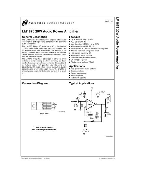
Connection Diagram<br />
Typical Applications<br />
Front View<br />
TLH5030–1<br />
Order Number <strong>LM1875</strong>T<br />
See NS Package Number T05B<br />
TLH5030–2<br />
C1995 National Semiconductor Corporation<br />
TLH5030<br />
RRD-B30M75Printed in U S A
Absolute Maximum Ratings<br />
If MilitaryAerospace specified devices are required<br />
please contact the National Semiconductor Sales<br />
OfficeDistributors for availability and specifications<br />
bV EE to V CC Input Voltage i JA<br />
73C<br />
Storage Temperature b65Ctoa150C<br />
Junction Temperature<br />
150C<br />
Supply Voltage<br />
60V<br />
Lead Temperature (Soldering 10 seconds) 260C<br />
i JC<br />
3C<br />
Electrical Characteristics<br />
V CC ea25V bV EE eb25V T AMBIENT e25C R L e8X A V e20 (26 dB) f o e1 kHz unless otherwise specified<br />
Parameter Conditions Typical Tested Limits Units<br />
Supply Current P OUT e0W 70 100 mA<br />
Output <strong>Power</strong> (Note 1) THDe1% 25 W<br />
THD (Note 1) P OUT e<strong>20W</strong> f o e1 kHz 0015 %<br />
P OUT e<strong>20W</strong> f o e20 kHz 005 04 %<br />
P OUT e<strong>20W</strong> R L e4Xf o e1 kHz 0022 %<br />
P OUT e<strong>20W</strong> R L e4Xf o e20 kHz 007 06 %<br />
Offset Voltage g1 g15 mV<br />
Input Bias Current g02 g2 mA<br />
Input Offset Current 0 g05 mA<br />
Gain-Bandwidth Product f o e20 kHz 55 MHz<br />
Open Loop Gain DC 90 dB<br />
PSRR V CC 1 kHz 1 Vrms 95 52 dB<br />
V EE 1 kHz 1 Vrms 83 52 dB<br />
Max Slew Rate <strong>20W</strong> 8X 70 kHz BW 8 Vms<br />
Current Limit V OUT e V SUPPLY b10V 4 3 A<br />
Equivalent Input Noise Voltage R S e600X CCIR 3 mVrms<br />
Note 1 Assumes the use of a heat sink having a thermal resistance of 1CW and no insulator with an ambient temperature of 25C Because the output limiting<br />
circuitry has a negative temperature coefficient the maximum output power delivered to a 4X load may be slightly reduced when the tab temperature exceeds<br />
55C<br />
Typical Applications (Continued)<br />
Typical Single Supply Operation<br />
TLH5030–3<br />
2
Typical Performance Characteristics<br />
<strong>Power</strong> Output vs Supply<br />
THD vs <strong>Power</strong> Output THD vs Frequency Voltage<br />
Supply Current vs Supply<br />
Voltage<br />
PSRR vs Frequency<br />
Device Dissipation vs<br />
Ambient Temperature<br />
<strong>Power</strong> Dissipation vs<br />
<strong>Power</strong> Output<br />
<strong>Power</strong> Dissipation vs<br />
<strong>Power</strong> Output<br />
wINTERFACE e 1CW<br />
See Application Hints<br />
I OUT vs V OUT -Current Limit<br />
Safe Operating Area Boundary<br />
Open Loop Gain and<br />
Phase vs Frequency<br />
Input Bias Current<br />
vs Supply Voltage<br />
Thermal shutdown with infinite heat sink<br />
Thermal shutdown with 1CW heat sink<br />
TLH5030–4<br />
3
Schematic Diagram<br />
TLH5030–5<br />
4
Application Hints<br />
STABILITY<br />
The <strong>LM1875</strong> is designed to be stable when operated at a<br />
closed-loop gain of 10 or greater but as with any other<br />
high-current amplifier the <strong>LM1875</strong> can be made to oscillate<br />
under certain conditions These usually involve printed circuit<br />
board layout or outputinput coupling<br />
Proper layout of the printed circuit board is very important<br />
While the <strong>LM1875</strong> will be stable when installed in a board<br />
similar to the ones shown in this data sheet it is sometimes<br />
necessary to modify the layout somewhat to suit the physical<br />
requirements of a particular application When designing<br />
a different layout it is important to return the load ground<br />
the output compensation ground and the low level (feedback<br />
and input) grounds to the circuit board ground point<br />
through separate paths Otherwise large currents flowing<br />
along a ground conductor will generate voltages on the conductor<br />
which can effectively act as signals at the input resulting<br />
in high frequency oscillation or excessive distortion<br />
It is advisable to keep the output compensation components<br />
and the 01 mF supply decoupling capacitors as close<br />
as possible to the <strong>LM1875</strong> to reduce the effects of PCB<br />
trace resistance and inductance For the same reason the<br />
ground return paths for these components should be as<br />
short as possible<br />
Occasionally current in the output leads (which function as<br />
antennas) can be coupled through the air to the amplifier<br />
input resulting in high-frequency oscillation This normally<br />
happens when the source impedance is high or the input<br />
leads are long The problem can be eliminated by placing a<br />
small capacitor (on the order of 50 pF to 500 pF) across the<br />
circuit input<br />
Most power amplifiers do not drive highly capacitive loads<br />
well and the <strong>LM1875</strong> is no exception If the output of the<br />
<strong>LM1875</strong> is connected directly to a capacitor with no series<br />
resistance the square wave response will exhibit ringing if<br />
the capacitance is greater than about 01 mF The amplifier<br />
can typically drive load capacitances up to 2 mF or so without<br />
oscillating but this is not recommended If highly capacitive<br />
loads are expected a resistor (at least 1X) should be<br />
placed in series with the output of the <strong>LM1875</strong> A method<br />
commonly employed to protect amplifiers from low impedances<br />
at high frequencies is to couple to the load through a<br />
10X resistor in parallel with a 5 mH inductor<br />
DISTORTION<br />
The preceding suggestions regarding circuit board grounding<br />
techniques will also help to prevent excessive distortion<br />
levels in audio applications For low THD it is also necessary<br />
to keep the power supply traces and wires separated<br />
from the traces and wires connected to the inputs of the<br />
<strong>LM1875</strong> This prevents the power supply currents which<br />
are large and nonlinear from inductively coupling to the<br />
<strong>LM1875</strong> inputs <strong>Power</strong> supply wires should be twisted together<br />
and separated from the circuit board Where these<br />
wires are soldered to the board they should be perpendicular<br />
to the plane of the board at least to a distance of a<br />
couple of inches With a proper physical layout THD levels<br />
at 20 kHz with 10W output to an 8X load should be less<br />
than 005% and less than 002% at 1 kHz<br />
CURRENT LIMIT AND SAFE OPERATING AREA (SOA)<br />
PROTECTION<br />
A power amplifier’s output transistors can be damaged by<br />
excessive applied voltage current flow or power dissipation<br />
The voltage applied to the amplifier is limited by the<br />
design of the external power supply while the maximum<br />
current passed by the output devices is usually limited by<br />
internal circuitry to some fixed value Short-term power dissipation<br />
is usually not limited in monolithic audio power amplifiers<br />
and this can be a problem when driving reactive<br />
loads which may draw large currents while high voltages<br />
appear on the output transistors The <strong>LM1875</strong> not only limits<br />
current to around 4A but also reduces the value of the limit<br />
current when an output transistor has a high voltage across<br />
it<br />
When driving nonlinear reactive loads such as motors or<br />
loudspeakers with built-in protection relays there is a possibility<br />
that an amplifier output will be connected to a load<br />
whose terminal voltage may attempt to swing beyond the<br />
power supply voltages applied to the amplifier This can<br />
cause degradation of the output transistors or catastrophic<br />
failure of the whole circuit The standard protection for this<br />
type of failure mechanism is a pair of diodes connected between<br />
the output of the amplifier and the supply rails These<br />
are part of the internal circuitry of the <strong>LM1875</strong> and needn’t<br />
be added externally when standard reactive loads are driven<br />
THERMAL PROTECTION<br />
The <strong>LM1875</strong> has a sophisticated thermal protection scheme<br />
to prevent long-term thermal stress to the device When the<br />
temperature on the die reaches 170C the <strong>LM1875</strong> shuts<br />
down It starts operating again when the die temperature<br />
drops to about 145C but if the temperature again begins to<br />
rise shutdown will occur at only 150C Therefore the device<br />
is allowed to heat up to a relatively high temperature if<br />
the fault condition is temporary but a sustained fault will<br />
limit the maximum die temperature to a lower value This<br />
greatly reduces the stresses imposed on the IC by thermal<br />
cycling which in turn improves its reliability under sustained<br />
fault conditions<br />
Since the die temperature is directly dependent upon the<br />
heat sink the heat sink should be chosen for thermal resistance<br />
low enough that thermal shutdown will not be reached<br />
during normal operation Using the best heat sink possible<br />
within the cost and space constraints of the system will improve<br />
the long-term reliability of any power semiconductor<br />
device<br />
POWER DISSIPATION AND HEAT SINKING<br />
The <strong>LM1875</strong> must always be operated with a heat sink<br />
even when it is not required to drive a load The maximum<br />
idling current of the device is 100 mA so that on a 60V<br />
power supply an unloaded <strong>LM1875</strong> must dissipate 6W of<br />
power The 54CW junction-to-ambient thermal resistance<br />
of a TO-220 package would cause the die temperature to<br />
rise 324C above ambient so the thermal protection circuitry<br />
will shut the amplifier down if operation without a heat<br />
sink is attempted<br />
5
Application Hints (Continued)<br />
In order to determine the appropriate heat sink for a given<br />
application the power dissipation of the <strong>LM1875</strong> in that application<br />
must be known When the load is resistive the<br />
maximum average power that the IC will be required to dissipate<br />
is approximately<br />
P D(MAX) V S 2<br />
2q2R L<br />
aP Q<br />
where V S is the total power supply voltage across the<br />
<strong>LM1875</strong> R L is the load resistance and P Q is the quiescent<br />
power dissipation of the amplifier The above equation is<br />
only an approximation which assumes an ‘‘ideal’’ class B<br />
output stage and constant power dissipation in all other<br />
parts of the circuit The curves of ‘‘<strong>Power</strong> Dissipation vs<br />
<strong>Power</strong> Output’’ give a better representation of the behavior<br />
of the <strong>LM1875</strong> with various power supply voltages and resistive<br />
loads As an example if the <strong>LM1875</strong> is operated on a<br />
50V power supply with a resistive load of 8X it can develop<br />
up to 19W of internal power dissipation If the die temperature<br />
is to remain below 150C for ambient temperatures up<br />
to 70C the total junction-to-ambient thermal resistance<br />
must be less than<br />
150Cb70C<br />
e42CW<br />
19W<br />
Using i JC e2CW the sum of the case-to-heat-sink interface<br />
thermal resistance and the heat-sink-to-ambient thermal<br />
resistance must be less than 22CW The case-toheat-sink<br />
thermal resistance of the TO-220 package varies<br />
with the mounting method used A metal-to-metal interface<br />
will be about 1CW if lubricated and about 12CW if dry<br />
Component Layouts<br />
Split Supply<br />
If a mica insulator is used the thermal resistance will be<br />
about 16CW lubricated and 34CW dry For this example<br />
we assume a lubricated mica insulator between the<br />
<strong>LM1875</strong> and the heat sink The heat sink thermal resistance<br />
must then be less than<br />
42CWb2CWb16CWe06CW<br />
This is a rather large heat sink and may not be practical in<br />
some applications If a smaller heat sink is required for reasons<br />
of size or cost there are two alternatives The maximum<br />
ambient operating temperature can be reduced to<br />
50C (122F) resulting in a 16CW heat sink or the heat<br />
sink can be isolated from the chassis so the mica washer is<br />
not needed This will change the required heat sink to a<br />
12CW unit if the case-to-heat-sink interface is lubricated<br />
Note When using a single supply maximum transfer of heat away from the<br />
<strong>LM1875</strong> can be achieved by mounting the device directly to the heat<br />
sink (tab is at ground potential) this avoids the use of a mica or other<br />
type insulator<br />
The thermal requirements can become more difficult when<br />
an amplifier is driving a reactive load For a given magnitude<br />
of load impedance a higher degree of reactance will cause<br />
a higher level of power dissipation within the amplifier As a<br />
general rule the power dissipation of an amplifier driving a<br />
60 reactive load (usually considered to be a worst-case<br />
loudspeaker load) will be roughly that of the same amplifier<br />
driving the resistive part of that load For example a loudspeaker<br />
may at some frequency have an impedance with a<br />
magnitude of 8X and a phase angle of 60 The real part of<br />
this load will then be 4X and the amplifier power dissipation<br />
will roughly follow the curve of power dissipation with a 4X<br />
load<br />
Single Supply<br />
TLH5030–6<br />
TLH5030–7<br />
6
<strong>LM1875</strong> <strong>20W</strong> <strong>Audio</strong> <strong>Power</strong> <strong>Amplifier</strong><br />
Physical Dimensions inches (millimeters)<br />
TO-220 <strong>Power</strong> Package (T)<br />
Order Number <strong>LM1875</strong>T<br />
NS Package Number T05B<br />
LIFE SUPPORT POLICY<br />
NATIONAL’S PRODUCTS ARE NOT AUTHORIZED FOR USE AS CRITICAL COMPONENTS IN LIFE SUPPORT<br />
DEVICES OR SYSTEMS WITHOUT THE EXPRESS WRITTEN APPROVAL OF THE PRESIDENT OF NATIONAL<br />
SEMICONDUCTOR CORPORATION As used herein<br />
1 Life support devices or systems are devices or 2 A critical component is any component of a life<br />
systems which (a) are intended for surgical implant support device or system whose failure to perform can<br />
into the body or (b) support or sustain life and whose be reasonably expected to cause the failure of the life<br />
failure to perform when properly used in accordance support device or system or to affect its safety or<br />
with instructions for use provided in the labeling can effectiveness<br />
be reasonably expected to result in a significant injury<br />
to the user<br />
National Semiconductor National Semiconductor National Semiconductor National Semiconductor National Semiconductores National Semiconductor<br />
Corporation GmbH Japan Ltd Hong Kong Ltd Do Brazil Ltda (Australia) Pty Ltd<br />
2900 Semiconductor Drive Livry-Gargan-Str 10 Sumitomo Chemical 13th Floor Straight Block Rue Deputado Lacorda Franco Building 16<br />
PO Box 58090 D-82256 F4urstenfeldbruck Engineering Center Ocean Centre 5 Canton Rd 120-3A Business Park Drive<br />
Santa Clara CA 95052-8090 Germany Bldg 7F Tsimshatsui Kowloon Sao Paulo-<strong>SP</strong> Monash Business Park<br />
Tel 1(800) 272-9959 Tel (81-41) 35-0 1-7-1 Nakase Mihama-Ku Hong Kong Brazil 05418-000 Nottinghill Melbourne<br />
TWX (910) 339-9240 Telex 527649 Chiba-City Tel (852) 2737-1600 Tel (55-11) 212-5066 Victoria 3168 Australia<br />
Fax (81-41) 35-1 Ciba Prefecture 261 Fax (852) 2736-9960 Telex 391-1131931 NSBR BR Tel (3) 558-9999<br />
Tel (043) 299-2300 Fax (55-11) 212-1181 Fax (3) 558-9998<br />
Fax (043) 299-2500<br />
National does not assume any responsibility for use of any circuitry described no circuit patent licenses are implied and National reserves the right at any time without notice to change said circuitry and specifications