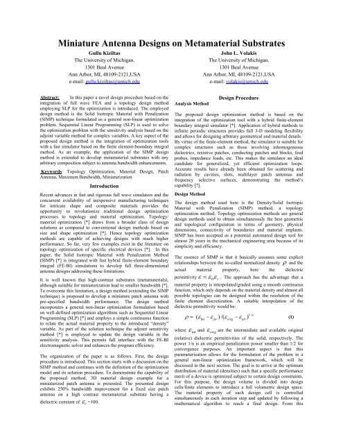
Miniature Antenna Designs on Metamaterial Substrates
Miniature Antenna Designs on Metamaterial Substrates
Miniature Antenna Designs on Metamaterial Substrates

Create successful ePaper yourself
Turn your PDF publications into a flip-book with our unique Google optimized e-Paper software.
<str<strong>on</strong>g>Miniature</str<strong>on</strong>g> <str<strong>on</strong>g>Antenna</str<strong>on</strong>g> <str<strong>on</strong>g>Designs</str<strong>on</strong>g> <strong>on</strong> <strong>Metamaterial</strong> <strong>Substrates</strong><br />
Gullu Kiziltas<br />
The University of Michigan.<br />
1301 Beal Avenue<br />
Ann Arbor, MI, 48109-2121,USA<br />
e-mail: gullu.kiziltas@umich.edu<br />
John L. Volakis<br />
The University of Michigan.<br />
1301 Beal Avenue<br />
Ann Arbor, MI, 48109-2121,USA<br />
e-mail: volakis@umich.edu<br />
Abstract: In this paper a novel design procedure based <strong>on</strong> the<br />
integrati<strong>on</strong> of full wave FEA and a topology design method<br />
employing SLP for the optimizati<strong>on</strong> is introduced. The employed<br />
design method is the Solid Isotropic Material with Penalizati<strong>on</strong><br />
(SIMP) technique formulated as a general n<strong>on</strong>-linear optimizati<strong>on</strong><br />
problem. Sequential Linear Programming (SLP) is used to solve<br />
the optimizati<strong>on</strong> problem with the sensitivity analysis based <strong>on</strong> the<br />
adjoint variable method for complex variables. A key aspect of the<br />
proposed design method is the integrati<strong>on</strong> of optimizati<strong>on</strong> tools<br />
with a fast simulator based <strong>on</strong> the finite element-boundary integral<br />
method. As an example, the applicati<strong>on</strong> of the SIMP design<br />
method is extended to develop metamaterial substrates with any<br />
arbitrary compositi<strong>on</strong> subject to antenna bandwidth enhancements.<br />
Keywords: Topology Optimizati<strong>on</strong>, Material Design, Patch<br />
<str<strong>on</strong>g>Antenna</str<strong>on</strong>g>, Maximum Bandwidth, Miniaturizati<strong>on</strong><br />
Introducti<strong>on</strong><br />
Recent advances in fast and rigorous full wave simulators and the<br />
c<strong>on</strong>current availability of inexpensive manufacturing techniques<br />
for intricate shape and composite materials provides the<br />
opportunity to revoluti<strong>on</strong>ize traditi<strong>on</strong>al design optimizati<strong>on</strong><br />
processes to topology and material optimizati<strong>on</strong>. Topology/<br />
material optimizati<strong>on</strong> [*] draws from a broader class of design<br />
soluti<strong>on</strong>s as compared to c<strong>on</strong>venti<strong>on</strong>al design methods based <strong>on</strong><br />
size and shape optimizati<strong>on</strong> [*]. Hence topology optimizati<strong>on</strong><br />
methods are capable of achieving designs with much higher<br />
performance. So far, very few examples exist in the literature <strong>on</strong><br />
topology optimizati<strong>on</strong> of specific electrical devices [*]. In this<br />
paper, the Solid Isotropic Material with Penalizati<strong>on</strong> Method<br />
(SIMP) [*] is integrated with fast hybrid finite-element boundary<br />
integral (FE-BI) simulati<strong>on</strong>s to develop full three-dimensi<strong>on</strong>al<br />
antenna designs addressing these limitati<strong>on</strong>s.<br />
It is well known that high-c<strong>on</strong>trast substrates (metamaterials),<br />
although suitable for miniaturizati<strong>on</strong> lead to smaller bandwidth [*].<br />
To overcome this limitati<strong>on</strong>, a design method (extending the SIMP<br />
technique) is proposed to develop a miniature patch antenna with<br />
pre-specified bandwidth performance. The design method<br />
incorporates a general n<strong>on</strong>-linear optimizati<strong>on</strong> formulati<strong>on</strong> based<br />
<strong>on</strong> well-defined optimizati<strong>on</strong> algorithms such as Sequential Linear<br />
Programming (SLP) [*] and employs a simple c<strong>on</strong>tinuous functi<strong>on</strong><br />
to relate the actual material property to the introduced “density”<br />
variable. As part of the soluti<strong>on</strong> technique the adjoint sensitivity<br />
method [*] is employed to update the design variable in the<br />
sensitivity analysis. This permits full interface with the FE-BI<br />
electromagnetic solver and enhances the program efficiency.<br />
The organizati<strong>on</strong> of the paper is as follows. First, the design<br />
procedure is introduced. This secti<strong>on</strong> starts with a discussi<strong>on</strong> <strong>on</strong> the<br />
SIMP method and c<strong>on</strong>tinues with the definiti<strong>on</strong> of the optimizati<strong>on</strong><br />
model and its soluti<strong>on</strong> procedure. To dem<strong>on</strong>strate the capability of<br />
the proposed method, 3D material design example for a<br />
miniaturized patch antenna is presented. The presented design<br />
exhibits 250% bandwidth improvement for a fixed size patch<br />
antenna <strong>on</strong> a high c<strong>on</strong>trast metamaterial substrate having a<br />
dielectric c<strong>on</strong>stant of ε<br />
r =100.<br />
Analysis Method<br />
Design Procedure<br />
The proposed design optimizati<strong>on</strong> method is based <strong>on</strong> the<br />
integrati<strong>on</strong> of the optimizati<strong>on</strong> tool with a hybrid finite-element<br />
boundary integral simulator [*]. Applicati<strong>on</strong> of hybrid methods to<br />
infinite periodic structures provides full 3-D modeling flexibility<br />
and allows for designing arbitrary geometrical and material details.<br />
By virtue of the finite-element method, the simulator is suitable for<br />
complex structures such as those involving inhomogeneous<br />
dielectrics, resistive patches, c<strong>on</strong>ducting patches and blocks, feed<br />
probes, impedance loads, etc. This makes the simulator an ideal<br />
candidate for generalized, yet efficient optimizati<strong>on</strong> loops.<br />
Accurate results have already been obtained for scattering and<br />
radiati<strong>on</strong> by cavities, slots, multilayer patch antennas and<br />
frequency selective surfaces, dem<strong>on</strong>strating the method’s<br />
capability [7].<br />
Design Method<br />
The design method used here is the Density/Solid Isotropic<br />
Material with Penalizati<strong>on</strong> (SIMP) method, a topology<br />
optimizati<strong>on</strong> method. Topology optimizati<strong>on</strong> methods are general<br />
design methods used to obtain simultaneously the best geometric<br />
and topological c<strong>on</strong>figurati<strong>on</strong> in terms of geometry, physical<br />
dimensi<strong>on</strong>s, c<strong>on</strong>nectivity of boundaries and material implants.<br />
SIMP has been accepted as a potential automated design tool for<br />
almost 20 years in the mechanical engineering area because of its<br />
simplicity and efficiency.<br />
The essence of SIMP is that it basically assumes some explicit<br />
relati<strong>on</strong>ships between the so-called normalized density ρ and the<br />
actual material property, here the dielectric<br />
permittivity ε = ε<br />
0ε<br />
r . The approach has the advantage that a<br />
material property is interpolated/graded using a smooth c<strong>on</strong>tinuous<br />
functi<strong>on</strong>, which <strong>on</strong>ly depends <strong>on</strong> the material density and almost all<br />
possible topologies can be designed within the resoluti<strong>on</strong> of the<br />
finite element discretizati<strong>on</strong>. A suitable interpolati<strong>on</strong> of the<br />
dielectric permittivity would be:<br />
ρ = ε −ε ε − ε<br />
(1)<br />
1/<br />
(<br />
int<br />
)/( ) n<br />
air orig air<br />
ε<br />
where ε<br />
int and orig are the intermediate and available original<br />
(relative) dielectric permittivities of the solid, respectively. The<br />
power 1/n is an empirical penalizati<strong>on</strong> power smaller than 1/2 for<br />
c<strong>on</strong>vergence purposes. An important aspect is that this<br />
parameterizati<strong>on</strong> allows for the formulati<strong>on</strong> of the problem in a<br />
general n<strong>on</strong>-linear optimizati<strong>on</strong> framework, which will be<br />
discussed in the next secti<strong>on</strong>. The goal is to arrive at the optimum<br />
distributi<strong>on</strong> of material (densities) such that a specific performance<br />
merit of a device is optimized subject to certain design c<strong>on</strong>straints.<br />
For this purpose, the design volume is divided into design<br />
cells/finite elements to introduce a full volumetric design space.<br />
The material property of each design cell is c<strong>on</strong>trolled<br />
simultaneously in each iterati<strong>on</strong> step and updated by following a<br />
mathematical algorithm to reach a final design. From this
viewpoint, a device is represented by material properties at every<br />
point in space via a single density variable.<br />
Optimizati<strong>on</strong> Model<br />
For our design problem, the specific goal is to determine the<br />
substrate material distributi<strong>on</strong> under a square patch antenna subject<br />
to pre-specified bandwidth and miniaturizati<strong>on</strong> requirements. An<br />
appropriate model for the corresp<strong>on</strong>ding topology optimizati<strong>on</strong><br />
problem employing the SIMP method would be to find the design<br />
variables ρ that minimize the cost functi<strong>on</strong>:<br />
f ρ = ⎡ s ⎤ j = N<br />
⎣ ⎦<br />
Subject to a material volume c<strong>on</strong>straint:<br />
( ) min max(<br />
11<br />
) 1,...<br />
j<br />
freq<br />
NFE<br />
∑ ρ⋅<br />
i<br />
Vi<br />
≤<br />
i=<br />
1<br />
V<br />
and side c<strong>on</strong>straints:<br />
min<br />
*<br />
0
Design Algorithm<br />
The ultimate algorithm for the proposed design cycle is displayed<br />
in Fig. 1. It c<strong>on</strong>sists of the following iterative steps: 1) Simulati<strong>on</strong><br />
of the device performance using the FE-BI solver with specified<br />
initial data, 2) Soluti<strong>on</strong> of the adjoint system equati<strong>on</strong>s of the<br />
original problem for the sensitivity analysis, 3) Optimizati<strong>on</strong> of the<br />
volumetric material distributi<strong>on</strong> of the dielectric substrate using an<br />
SLP algorithm and 4) Updating the design variables<br />
(densities/permittivities) relying <strong>on</strong> the interpolati<strong>on</strong> scheme of the<br />
SIMP design method. C<strong>on</strong>vergence is achieved when the changes<br />
in the objective functi<strong>on</strong> value drops below a certain value like<br />
0.001. Specified initial data include design variables, which<br />
corresp<strong>on</strong>d to an initial homogenous dielectric substrate with a<br />
certain permittivity value. Certain design parameters are also<br />
specified at this step but do not change during the design cycle.<br />
These are the patch geometry and material characterizati<strong>on</strong>, like<br />
the dielectric block dimensi<strong>on</strong>s. Also, the feed locati<strong>on</strong> and<br />
amplitude and the frequency range of operati<strong>on</strong> are specified.<br />
Initial design<br />
variables<br />
Field<br />
Analysis<br />
(FE code)<br />
Sensitivity<br />
Computati<strong>on</strong><br />
Variable change<br />
Via density method<br />
Optimizati<strong>on</strong> Solver<br />
(SLP)<br />
Fig. 1 Design Optimizati<strong>on</strong> Flowchart<br />
C<strong>on</strong>verge?<br />
NO<br />
YES<br />
Optimal<br />
topology<br />
Design Example<br />
The main goal here is to improve the bandwidth performance of a<br />
chosen simple patch antenna by designing its substrate material<br />
employing the design procedure outlined above. As is well known,<br />
microstrip patch antennas are attractive, low- weight, low-profile<br />
antennas, which however suffer from low bandwidth. Moreover, its<br />
bandwidth is further reduced as the substrate dielectric c<strong>on</strong>stant is<br />
increased for miniaturizati<strong>on</strong>. In this secti<strong>on</strong>, we will dem<strong>on</strong>strate<br />
bandwidth improvement of a chosen simple patch antenna by<br />
introducing a new (metamaterial) substrate texture whose<br />
properties are not found in nature.<br />
2.5<br />
3.175<br />
1.25<br />
1.25<br />
2.5<br />
0.625<br />
Fig. 2 Schematic of the patch antenna <strong>on</strong> the dielectric block<br />
substrate (dimensi<strong>on</strong>s are in cm).<br />
The chosen geometry is a square patch fed with a probe/coax feed<br />
and the details of the whole structure are displayed in Fig. 2. The<br />
frequency range of interest is 1-2 GHz sampled over 21 frequency<br />
points. For this design, the volume was set to 70% with respect to<br />
the initial substrate dielectric permittivity to ensure better<br />
miniaturizati<strong>on</strong> for the designed substrate. The volume c<strong>on</strong>straint is<br />
also necessary to avoid trivial bandwidth improvement via lower<br />
dielectric c<strong>on</strong>stant.<br />
Fig. 3 Optimally designed metamaterial texture<br />
The initial design using a homogenous substrate having ε =42<br />
resulted in a 5dB return loss bandwidth of 6.7% and we were not<br />
able to obtain the typical 10dB bandwidth because of the capacitive<br />
nature of the high c<strong>on</strong>trast material. By pursuing the above<br />
discussed design procedures, with each design cell being updated<br />
via the SIMP method and the SLP routine, a heterogeneous design<br />
was obtained in 20 iterati<strong>on</strong>s. The c<strong>on</strong>verged material distributi<strong>on</strong><br />
is displayed in Fig. 3 as a 3D color coded block with each color<br />
pixel corresp<strong>on</strong>ding to a certain density/permittivity value. The<br />
corresp<strong>on</strong>ding return loss behavior of the optimized dielectric<br />
distributi<strong>on</strong> is depicted in Fig. 4 and compared to the initial<br />
performance.<br />
Return Loss (dB)<br />
0<br />
-5<br />
-10<br />
-15<br />
-20<br />
-25<br />
-30<br />
Initial<br />
Optimized design *<br />
Fabricated --<br />
6.7%<br />
19%<br />
17%<br />
11% 14%<br />
1.4 1.6 1.8 2<br />
Freq (GHz)<br />
Fig. 4 Return loss behavior for initial and designed textured<br />
substrate<br />
The computati<strong>on</strong> time for the entire design process with a design<br />
domain of 4000 finite elements/design cells and 21 frequency<br />
points for each iterati<strong>on</strong> was 17 hours <strong>on</strong> a Pentium 3 Processor.<br />
Given the poor bandwidth at the starting point of the design, the<br />
attained bandwidth performance (with material design <strong>on</strong>ly) is<br />
truly remarkable.<br />
To fabricate the design, certain post processing/image processing<br />
needed to be applied <strong>on</strong> the design to transform it into a two<br />
material composite of available material. Adaptive Image<br />
Processing with a simple filtering idea based <strong>on</strong> a cut-off value of<br />
0.64 for the densities has been adapted to solidify and fabricate the<br />
3D material composite substrate (Fig. 5) using Thermoplastic<br />
Green Machining. More specifically, first a thermoplastic<br />
compound was prepared by mixing commercially available lowtemperature<br />
cofirable ceramic (ULF 101) powder with melted<br />
binder systems. Once compounded, it was warm-pressed and the<br />
dielectric block in its “green body” state was obtained. The<br />
material is machinable at this stage and has slightly larger<br />
dimensi<strong>on</strong>s than the original design. After removing material via a<br />
computer-c<strong>on</strong>trolled equipment (Modela; Roland DG Corp., Japan)<br />
according to the filtered design geometry, this substrate is sintered.<br />
During machining, it is also slightly modified for machinability
and c<strong>on</strong>sidering shrinkage after sintering. The return loss behavior<br />
of the fabricated design compared to the initial substrate and the<br />
volumetric graded design. It is important to note that the attained<br />
BW has slightly changed for the fabricated design. This<br />
dem<strong>on</strong>strates the power of integrating robust optimizati<strong>on</strong><br />
techniques with simple filtering processes for manufacturable<br />
substrates with desired performance.<br />
[8]S. S. Rao, Engineering Optimizati<strong>on</strong>: Theory and Practice, 3 rd ed. New<br />
York, Wiley, 1996<br />
[9]H. C. Gea, “Topology Optimizati<strong>on</strong>: A new microstructure-based design<br />
domain method,” Computers and Structures, vol. 61, no.5, pp.781-788,<br />
1996<br />
[10]R. Hans<strong>on</strong> and K. Hiebert, “A sparse linear programming<br />
subprogram,” Technical Report SAND81-0297, Sandia Nati<strong>on</strong>al<br />
Laboratories, 1981<br />
Fig. 5<br />
C<strong>on</strong>clusi<strong>on</strong><br />
The aim of this paper was to dem<strong>on</strong>strate the capability of<br />
designing for metamaterial substrates using the SIMP method. This<br />
has been d<strong>on</strong>e by designing for variable material substrates to<br />
improve antenna performance and more specifically bandwidth.<br />
The design is also filtered and solidified to achieve a<br />
manufacturable design. To achieve a 250% improvement in a fixed<br />
size patch antenna, the SIMP method has been extended al<strong>on</strong>g with<br />
the SLP routine for the soluti<strong>on</strong>. Key to the success of the<br />
optimizati<strong>on</strong> was the integrati<strong>on</strong> of optimizati<strong>on</strong> tool with fast, full<br />
wave FE-BI solver and the utilizati<strong>on</strong> of the sensitivity analysis.<br />
The fabricated final design using TGM dem<strong>on</strong>strates, by virtue of<br />
the generality and efficiency of the proposed method, there is great<br />
potential for improving antenna performance or other RF devices.<br />
References<br />
[1] J.M. Johns<strong>on</strong> and Y. Rahmat-Samii, “Genetic algorithms and method of<br />
moments (GA/MoM) for the design of integrated antennas,” IEEE<br />
Transacti<strong>on</strong>s <strong>on</strong> <str<strong>on</strong>g>Antenna</str<strong>on</strong>g>s and Propagati<strong>on</strong>, vol. 47, no. 10, pp. 1606-<br />
1614, October 1999<br />
[2] E. Michielssen, J. M. Sajer, S. Ranjithan, R. Mittra, “Design of lightweight,<br />
broad-band microwave absorbers using genetic algorithms,” IEEE<br />
Transacti<strong>on</strong>s <strong>on</strong>. Microwave Theory and Techniques, vol. 41, no. 6/7, pp.<br />
1024-1031, 1993.<br />
[3] Z. Li, Y. E. Erdemli, J.L. Volakis and P.Y. Papalambros, “Design<br />
Optimizati<strong>on</strong> of C<strong>on</strong>formal <str<strong>on</strong>g>Antenna</str<strong>on</strong>g>s by Integrating Stochastic Algorithms<br />
With the Hybrid Finite-Element Method ,” IEEE Transacti<strong>on</strong>s <strong>on</strong> <str<strong>on</strong>g>Antenna</str<strong>on</strong>g>s<br />
Propagai<strong>on</strong>, vol. 50, no. 5, May 2002<br />
[4] D. N. Dyck, D. A. Lowther and E. M. Freeman, “A method of<br />
Computing the Sensitivity in Electromagnetic Quantities to changes in<br />
Materials and Sources,” vol. 30, no. 5, Sept. 1994<br />
[5]J. Yoo and Noboru Kikuchi, “Topology Optimizati<strong>on</strong> in magnetic fields<br />
using the homogenizati<strong>on</strong> design method,” Internati<strong>on</strong>al Journal for<br />
Numerical Methods in Engineering, vol. 48, pp. 1463-1479, 2000<br />
[6] O. Sigmund, “Design of multi-physics actuators using topology<br />
optimizati<strong>on</strong>- Part I: One material structures”, Computer methods in<br />
applied mechanics and engineering, vol. 190, pp. 6577-6604, 2001<br />
[7] T. F. Eibert and J. L. Volakis, “Fast spectral domain algorithm<br />
forhybrid finite element / boundary integral modeling of doubly periodic<br />
structures,” IEEE Proceedings: Microwaves, <str<strong>on</strong>g>Antenna</str<strong>on</strong>g>s and Propagati<strong>on</strong>,<br />
vol. 147, no. 5, pp. 329-334, October 2000