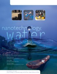
Small size - large impact - Nanowerk
Small size - large impact - Nanowerk
Small size - large impact - Nanowerk

Create successful ePaper yourself
Turn your PDF publications into a flip-book with our unique Google optimized e-Paper software.
24<br />
Myth 1: Nanotechnology is a distinct,<br />
previously unknown discipline<br />
Nanotechnology actually embraces advancements over<br />
a wide range of scientific and technical disciplines –<br />
physics, chemistry, biology, materials science, mechanics,<br />
and electronics, to name just a few. Commonly<br />
designated as the science and technology in which at least<br />
one dimension is controlled to less than 100 nanometers,<br />
it may, in fact, be best to think of nanotechnology as<br />
an engineering discipline: its aim is to design and build<br />
structures and devices on this very small-length scale<br />
using tools from whatever field is appropriate.<br />
Although the word is relatively new, nanotechnology<br />
has been around for some time. Chemists and biologists,<br />
for example, have long been able to design and create<br />
molecules with specific atomic structures. Typically,<br />
this could be done only in batches with relatively <strong>large</strong><br />
collections of molecules. Over the past 20 years or<br />
so, scientists and engineers have increasingly extended<br />
the ability to view and manipulate ever smaller bits<br />
of matter – in some cases individual atoms. While<br />
nanoparticle additives to paints and clothing,<br />
molecular circuit elements and designer drugs can<br />
all be considered nanotechnologies, these applications<br />
have little in common beyond their use of materials<br />
designed and structured at the nanometer scale.<br />
In the IT industry, semiconductor manufacturers are<br />
now producing chips with minimum lithographic<br />
dimensions which measure a mere 90 nanometers or<br />
less and feature millions of transistors. The experimental<br />
silicon transistors in our laboratories are smaller yet. A<br />
mere 6 nanometers for the critical gate length is the current<br />
frontier – the kind of innovation that IT relies upon<br />
to build devices that are ever smaller, faster and cheaper.<br />
Myth 2: The primary goal of nanotechnololgy<br />
is to create self-assembling nanobots<br />
Researchers today are hardly creating the self-replicating<br />
nanobots of science fiction, Instead, they are working<br />
on the so-called directed self-assembly of nanoscale<br />
materials and devices, aiming to exploit the natural<br />
tendency of atoms and molecules to orient themselves,<br />
react, and bind with each other in predictable ways<br />
under the right conditions.<br />
Self-assembly is nothing other than exploitation of<br />
the laws of thermodynamics and kinetics which drive<br />
all natural phenomena. Consider a snowflake, which<br />
is created when water molecules floating in a cloud<br />
coalesce around a grain of dust and crystallize to create<br />
a new structure. While a snowflake may have a complex<br />
structure, it is far from alive and does not self-replicate.<br />
Nevertheless, when conditions are right, nature makes<br />
trillions of them quickly and cheaply.<br />
By taking advantage of such natural forces, scientists try<br />
to discover the conditions to form technologically useful<br />
new materials and devices. They are currently exploring<br />
the directed assembly of transistors and circuits based<br />
on carbon nanotubes, semiconductor nanowires and<br />
molecular building blocks. Further, they are developing<br />
self-assembled materials for data storage and memory.<br />
In the future, processes of directed self-assembly are<br />
likely to be used increasingly in combination with<br />
today’s photolithography to reduce the reliance on this<br />
ever more expensive method for semiconductor<br />
manufacturing. In this sense, the often-cited contrast<br />
between top-down (photolithography) versus bottom-up<br />
(self-assembly) approaches to device fabrication is a false<br />
dichotomy. A hybrid of the two already is – and will<br />
continue to be – employed.<br />
Myth 3: Nanotechnology will<br />
replace microelectronics<br />
Microelectronics is a nanotechnology, as are hard-disk<br />
drives whose giant-magnetoresistive read heads and<br />
magnetic media rely on layers of materials only a few<br />
atoms thick to give computers ever more storage capacity.<br />
Rather than suddenly replacing today’s methods for<br />
chip manufacture, it is more likely that individual<br />
nanostructures and nanodevices and new manufacturing<br />
processes will increasingly be integrated into the<br />
mainstream. Transistors made out of the new materials<br />
being considered, such as carbon nanotubes and<br />
semiconductor nanowires, might not be much smaller<br />
than that experimental 6-nanometer silicon transistor<br />
mentioned above. Silicon probably has a promising<br />
future as a nanomaterial.<br />
That being said, there are numerous, innovative<br />
alternatives being explored to augment the capabilities<br />
of integrated circuits. Particularly interesting is the<br />
prospect of using physical phenomena other than simple<br />
manipulation of electronic charge in future computing<br />
devices, such as the spin of electrons (so-called<br />
spintronics) or even nanoscale mechanics.<br />
Challenges and opportunities for the future<br />
of the IT industry<br />
While nanotechnology is already contributing to<br />
the ongoing progress and extension of IT technology,<br />
the future is not without its challenges. The scaling<br />
of semiconductor technology known as Moore’s Law<br />
may continue for another decade or so, allowing us to<br />
eventually fabricate transistors with critical dimensions<br />
approaching 10 nanometer. After that, a transition<br />
in technological hardware and, a long lead-time for<br />
developing new technologies can be expected. As such,<br />
the IT industry is working now on the successor to<br />
conventional CMOS semiconductor technology.