- Page 1 and 2:
POWER MANAGEMENT ICS DC/DC Switchin
- Page 3 and 4:
All data shown in this catalog is s
- Page 5 and 6:
Surface Mount Schottky / SBR ® Rec
- Page 7 and 8:
3000W Transient Voltage Suppressors
- Page 9 and 10:
6.0A Ultra-Fast Recovery Glass Pass
- Page 11 and 12:
For package outline drawings and su
- Page 13 and 14:
Power Management ICs DC/DC Switchin
- Page 15 and 16:
Power Management ICs Linear Regulat
- Page 17 and 18:
Power Management ICs Shunt Voltage
- Page 19 and 20:
Power Management ICs Op Amp / Compa
- Page 21 and 22:
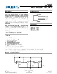
Hall Effect Sensors Hall-Effect Sen
- Page 23 and 24:
Hall Effect Sensors Hall-Effect Sen
- Page 25 and 26:
Schottky / SBR ® Diodes Discrete S
- Page 27 and 28:
Schottky / SBR ® Diodes Discrete S
- Page 29 and 30:
Discrete Semiconductors Surface Mou
- Page 31 and 32:
Discrete Semiconductors Surface Mou
- Page 33 and 34:
Discrete Semiconductors Surface Mou
- Page 35 and 36:
Discrete Semiconductors Through-Hol
- Page 37 and 38:
Discrete Semiconductors Through-Hol
- Page 39 and 40:
Discrete Semiconductors Through-Hol
- Page 41 and 42:
Discrete Semiconductors Through-Hol
- Page 43 and 44:
Discrete Semiconductors Switching D
- Page 45 and 46:
Discrete Semiconductors Switching D
- Page 47 and 48:
Discrete Semiconductors Zener Diode
- Page 49 and 50:
Discrete Semiconductors Zener Diode
- Page 51 and 52:
Discrete Semiconductors Zener Diode
- Page 53 and 54:
Discrete Semiconductors Zener Diode
- Page 55 and 56:
Discrete Semiconductors Zener Diode
- Page 57 and 58:
Discrete Semiconductors Zener Diode
- Page 59 and 60:
Discrete Semiconductors Zener Diode
- Page 61 and 62:
Discrete Semiconductors Zener Diode
- Page 63 and 64:
Discrete Semiconductors Zener Diode
- Page 65 and 66:
Discrete Semiconductors Zener Diode
- Page 67 and 68:
Discrete Semiconductors Transient V
- Page 69 and 70:
Discrete Semiconductors Transient V
- Page 71 and 72:
Discrete Semiconductors Transient V
- Page 73 and 74:
Discrete Semiconductors Transient V
- Page 75 and 76:
Discrete Semiconductors Thyristor S
- Page 77 and 78:
Discrete Semiconductors Thyristor S
- Page 79 and 80:
Discrete Semiconductors Part Number
- Page 81 and 82:
Discrete Semiconductors Part Number
- Page 83 and 84:
Discrete Semiconductors Part Number
- Page 85 and 86:
Discrete Semiconductors Matched Pai
- Page 87 and 88:
Discrete Semiconductors NPN, PNP Pr
- Page 89 and 90:
Discrete Semiconductors NPN, PNP Pr
- Page 91 and 92:
Discrete Semiconductors Part Number
- Page 93 and 94:
Discrete Semiconductors Part Number
- Page 95 and 96:
Discrete Semiconductors Complex Arr
- Page 97 and 98:
Discrete Semiconductors Part Number
- Page 99 and 100:
Discrete Semiconductors Super-Fast
- Page 101 and 102: Discrete Semiconductors Super-Fast
- Page 103 and 104: Discrete Semiconductors Super-Fast
- Page 105 and 106: Discrete Semiconductors Super-Fast
- Page 107 and 108: Discrete Semiconductors Standard Re
- Page 109 and 110: Discrete Semiconductors Standard Re
- Page 111 and 112: Discrete Semiconductors Standard Re
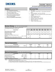
- Page 113 and 114: Bridge Rectifiers Discrete Semicond
- Page 115 and 116: Bridge Rectifiers Discrete Semicond
- Page 117 and 118: Bridge Rectifiers Discrete Semicond
- Page 119 and 120: Product Packaging Information DFN14
- Page 121 and 122: Product Packaging Information DFN20
- Page 123 and 124: Product Packaging Information MSOP-
- Page 125 and 126: Product Packaging Information SOD-5
- Page 127 and 128: Product Packaging Information SOT-3
- Page 129 and 130: Product Packaging Information TO252
- Page 131 and 132: Product Packaging Information Axial
- Page 133 and 134: Not Through Holes Product Packaging
- Page 135 and 136: Product Packaging Information PBPC-
- Page 137 and 138: Product Packaging Information SIP-3
- Page 139 and 140: Product Packaging Information TO220
- Page 141 and 142: Product Packaging Information SUGGE
- Page 143 and 144: Product Packaging Information Figur
- Page 145 and 146: Product Packaging Information Figur
- Page 147 and 148: Product Packaging Information Figur
- Page 149 and 150: KXXKXX KXXKXX KXXKXX 8mm Product Pa
- Page 151: Product Packaging Information Tape
- Page 155 and 156: Product Packaging Information THROU
- Page 157 and 158: Product Packaging Information PRODU
- Page 159 and 160: STANDARD PRODUCT LABEL (Analog Prod
- Page 161 and 162: Product Packaging Information Outer
- Page 163 and 164: Product Packaging Information PRODU
- Page 165 and 166: Alphanumeric Part Number Index Inde
- Page 167 and 168: Alphanumeric Part Number Index Inde
- Page 169 and 170: Alphanumeric Part Number Index Inde
- Page 171 and 172: Alphanumeric Part Number Index Inde
- Page 173: Alphanumeric Part Number Index Inde