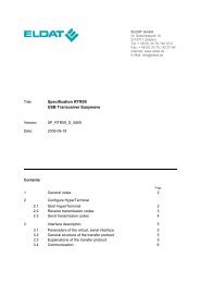
Specification of RTRM08 Transceiver Module Easywave I2C - ELDAT
Specification of RTRM08 Transceiver Module Easywave I2C - ELDAT
Specification of RTRM08 Transceiver Module Easywave I2C - ELDAT

You also want an ePaper? Increase the reach of your titles
YUMPU automatically turns print PDFs into web optimized ePapers that Google loves.
<strong>Specification</strong><br />
Index 1.01<br />
Project No.<br />
RF-Products, Controller <strong>RTRM08</strong> <strong>Transceiver</strong> <strong>Module</strong> Easw I 2 C Page 1<br />
Development<br />
Production S. Schreiber 2007-08-24<br />
<strong>Specification</strong><br />
<strong>of</strong><br />
<strong>RTRM08</strong><br />
<strong>Transceiver</strong> <strong>Module</strong><br />
<strong>Easywave</strong> I 2 C<br />
7007
<strong>Specification</strong><br />
Index 1.01<br />
Project No.<br />
RF-Products, Controller <strong>RTRM08</strong> <strong>Transceiver</strong> <strong>Module</strong> Easw I 2 C Page 2<br />
Development<br />
Production S. Schreiber 2007-08-24<br />
Revision History<br />
Index Releases<br />
0.90 Initial Release.<br />
1.00 Section 1 and section 2.1:<br />
Options for the antenna are mentioned now.<br />
Section 2.3:<br />
7007<br />
Some figures have been corrected. The acknowledge bit A- after the final data byte <strong>of</strong><br />
a read transfer is labeled with “1“ now (Figure 4, Figure 5, Figure 7, Figure 8).<br />
It is stated now that the current implementation interrupts any receive attempt <strong>of</strong><br />
<strong>Easywave</strong> telegrams while the persistent storage is written (RX_USERDATA0 and<br />
RX_USERDATA1 registers).<br />
It is stated that any bit is cleared in the RX_LN_CHXXX registers when <strong>ELDAT</strong> ships the<br />
transceiver module <strong>RTRM08</strong>.<br />
1.01 Section 1, section 2.1, and section 3.2:<br />
The upper limit <strong>of</strong> the power supply's operational range <strong>of</strong> 5.5 V has been decreased to<br />
5.25 V.
<strong>Specification</strong><br />
Index 1.01<br />
Project No.<br />
RF-Products, Controller <strong>RTRM08</strong> <strong>Transceiver</strong> <strong>Module</strong> Easw I 2 C Page 3<br />
Development<br />
Production S. Schreiber 2007-08-24<br />
Table <strong>of</strong> Contents<br />
1 General Description...........................................................................................................................4<br />
2 Functional Description...................................................................................................................... 4<br />
2.1 Pin Definition.............................................................................................................................4<br />
2.2 Power up and Reset....................................................................................................................5<br />
2.3 <strong>I2C</strong>-bus.......................................................................................................................................5<br />
Signal Lines <strong>of</strong> the <strong>I2C</strong>-bus........................................................................................................5<br />
Addressing a Slave and Performing Data Transfer....................................................................6<br />
Accessing the <strong>Transceiver</strong> <strong>Module</strong>.......................................................................................... 12<br />
Initialization on Reset.............................................................................................................. 19<br />
Receiving <strong>of</strong> <strong>Easywave</strong> Telegrams.......................................................................................... 19<br />
Learning <strong>of</strong> <strong>Easywave</strong> Telegrams............................................................................................ 21<br />
Delete Learned <strong>Easywave</strong> Telegrams.......................................................................................21<br />
Transmitting <strong>of</strong> <strong>Easywave</strong> Telegrams......................................................................................22<br />
3 Electrical Characteristics................................................................................................................. 23<br />
3.1 Absolute Maximum Ratings.................................................................................................... 23<br />
3.2 Operating Conditions...............................................................................................................23<br />
3.3 Characteristics..........................................................................................................................24<br />
4 Mechanical <strong>Specification</strong>................................................................................................................ 24<br />
Figures<br />
Figure 1 Component side view <strong>of</strong> the transceiver module................................................................... 4<br />
Figure 2 <strong>I2C</strong>-bus lines and common conditions...................................................................................6<br />
Figure 3 Write transfer using a 7-bit address........................................................................................7<br />
Figure 4 Read transfer using a 7-bit address.........................................................................................7<br />
Figure 5 Combined write and read transfer using a 7-bit address........................................................ 8<br />
Figure 6 Write transfer using a 10-bit address....................................................................................10<br />
Figure 7 Read transfer using a 10-bit address.....................................................................................11<br />
Figure 8 Combined write and read transfer using a 10-bit address.................................................... 12<br />
Figure 9 Writing into registers <strong>of</strong> the transceiver module..................................................................13<br />
Figure 10 Reading out registers <strong>of</strong> the transceiver module................................................................ 13<br />
Figure 11 Sequence when receiving <strong>Easywave</strong> telegrams..................................................................20<br />
Figure 12 Sequence when transmitting <strong>Easywave</strong> telegrams............................................................. 23<br />
Figure 13 Drawing <strong>of</strong> the transceiver module.................................................................................... 26<br />
7007
<strong>Specification</strong><br />
Index 1.01<br />
Project No.<br />
RF-Products, Controller <strong>RTRM08</strong> <strong>Transceiver</strong> <strong>Module</strong> Easw I 2 C Page 4<br />
Development<br />
Production S. Schreiber 2007-08-24<br />
1 General Description<br />
Features <strong>of</strong> the <strong>RTRM08</strong> transceiver module:<br />
– Sends and receives <strong>Easywave</strong> at 868.3 MHz, FSK modulation.<br />
– Whip antenna. Other options are available on request: coaxial connectors or an antenna via the module's<br />
connector.<br />
– High output power <strong>of</strong> +9 dBm (at 5 V power supply) .<br />
– Each module can transmit 32 different <strong>Easywave</strong> telegrams which have unique serial numbers.<br />
– Up to 32 <strong>Easywave</strong> transmitters can be taught in the <strong>RTRM08</strong> <strong>Easywave</strong> module. The <strong>RTRM08</strong> stores<br />
16-bit user data associated with each <strong>Easywave</strong> transmitter. Persistent storage (EEPROM).<br />
– I 2 C-bus, 100 kHz clock rate (Standard Mode), slave only.<br />
– Fixed I 2 C address, which is 1100010 (7-bit, excluding the R/W-bit).<br />
– A separate request output allows to work without any polling.<br />
– Operational range <strong>of</strong> power supply: 2.1 V to 5.25 V.<br />
– Power down state with low current consumption when being inactive.<br />
– LEDs indicate transmit and receive operation (optional).<br />
– Approval standards EN 300 220-1 V1.3.1 (2000-09) and EN 300 220-3 V1.1.1 (2000-09).<br />
2 Functional Description<br />
2.1 Pin Definition<br />
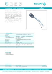
Pins are numbered as shown in Figure 1.<br />
LED (receive, green)<br />
LED (transmit, yellow)<br />
1 2 3 4 5 6 7 8 9 10 11 12<br />
whip antenna<br />
Figure 1 Component side view <strong>of</strong> the transceiver module<br />
7007
<strong>Specification</strong><br />
Index 1.01<br />
Project No.<br />
RF-Products, Controller <strong>RTRM08</strong> <strong>Transceiver</strong> <strong>Module</strong> Easw I 2 C Page 5<br />
Development<br />
Production S. Schreiber 2007-08-24<br />
Pin number Signal name Signal direction Description<br />
1 VCC - Power supply (2.1 V ...5.25 V).<br />
2 GND - Ground.<br />
3 / RESET in Reset. Active low.<br />
4 SDA bidirectional (open-drain) I 2 C serial data I/O.<br />
5 SCL bidirectional (open-drain) I 2 C synchronous serial clock I/O.<br />
6 / REQ out (open-drain) Request output. It indicates whether an<br />
<strong>Easywave</strong> telegram could be received and<br />
whether a received <strong>Easywave</strong> telegram is<br />
over. Active low.<br />
7 - 12 (NC) - Pins are not allowed to connect to any circuit.<br />
There are options for the antenna available, for example, coaxial connectors or an antenna via the module's<br />
connector. Please contact <strong>ELDAT</strong>.<br />
2.2 Power up and Reset<br />
The module's / RESET signal is not allowed to be high until the power supply is in the operational range. The<br />
module is in inactive state subsequently; it can be controlled via the I 2 C-bus.<br />
The / REQ output <strong>of</strong> the module goes to (active) low until the module's rx mode is altered.<br />
The module also can be reset at any time independent from its former state by asserting the / RESET signal.<br />
2.3 I 2 C-bus<br />
The SCL and the SDA pin are the I 2 C-bus as defined in the “THE I 2 C-BUS SPECIFICATION VERSION 2.1“<br />
(January 2000), document order number 9398 393 40011 by Philips.<br />
A short discussion <strong>of</strong> the I 2 C-bus follows in this section. If both this specification <strong>of</strong> the <strong>RTRM08</strong> transceiver<br />
module and the referred “THE I 2 C-BUS SPECIFICATION VERSION 2.1“ document define a specific detail,<br />
the specification <strong>of</strong> the <strong>RTRM08</strong> transceiver module has informational characteristics only.<br />
The I 2 C clock rate <strong>of</strong> the transceiver module can be up to 100 kHz (Standard Mode).<br />
Signal Lines <strong>of</strong> the I 2 C-bus<br />
The I 2 C-bus is a 2-wire bus; it has a bidirectional serial clock line SCL and a bidirectional serial data line SDA.<br />
Both SCL and SDA are combined inputs and open-drain outputs. There must be one pullup-resistor on each<br />
<strong>of</strong> the SCL and the SDA line. The <strong>RTRM08</strong> transceiver module I 2 C PHY does not include these pullupresistors.<br />
A device connected to a bus can be either a master or a slave. A master device is able to acquire the I 2 C-bus<br />
and initiate a transfer from (read) or to (write) a specified slave. The master generates the clock on the SCL<br />
line in order to transfer the serial data bits. The slave can slow down the transfer if it can't transmit or receive<br />
data bytes fast enough (clock stretching, see below). The master has to terminate the transfer and release<br />
the I 2 C-bus either successfully or due to a fail.<br />
The SDA line is driven by the device which transmits data bits: it is either a master or a slave.<br />
One or more master devices can be connected to the I 2 C-bus. This specification covers examples with one<br />
master only, but the transceiver module also works on I 2 C-busses with more than one master (multi-master).<br />
7007
<strong>Specification</strong><br />
Index 1.01<br />
Project No.<br />
RF-Products, Controller <strong>RTRM08</strong> <strong>Transceiver</strong> <strong>Module</strong> Easw I 2 C Page 6<br />
Development<br />
Production S. Schreiber 2007-08-24<br />
Furthermore, one or more slave devices are connected to the I 2 C-bus, where each slave device must have a<br />
unique I 2 C-address.<br />
An I 2 C bus can be free and there are start conditions, repeated start conditions, stop conditions, and bit<br />
transfers on an I 2 C-bus (Figure 2).<br />
Both SCL and SDA are high while the I 2 C bus is free; all <strong>of</strong> the SCL and SDA outputs are high. (All open-drain<br />
outputs on a line form a wired-AND.)<br />
The start condition S is a falling edge <strong>of</strong> the SDA line, when the SCL line is (still) high. The SCL line is pulled to<br />
low subsequently. A start condition S is generated only by a master.<br />
The SCL line is low before a bit transfer (subsequent to a start condition or a bit transfer). The transmitting<br />
device pulls the SDA line low or releases it to high according to the desired data bit first. At next the master<br />
generates a rising edge on the SCL line and a falling edge on SCL subsequently. (When SCL is high between<br />
the rising and falling edge, SDA must not change its state, because it would generate a start condition or a<br />
stop condition.) The SCL line is low again after transmitting the bit. The SCL line is always driven by the<br />
master, but the SDA line is driven by the transmitting device (either the master or the slave which was<br />
addressed before by the master).<br />
A slave can slow down the transfer by pulling the SCL line to low after the falling edge (clock stretching). The<br />
master has to realize that the slave pulls the SCL line to low. Since the SCL outputs <strong>of</strong> the master and the<br />
slave form a wired-AND, the SCL line will be low until both the master and the slave are able to continue.<br />
The SCL line is low before a stop condition P (subsequent to a bit transfer). The SDA line is pulled to low if it<br />
was not low before. The SCL line is released to high. A rising edge is generated on the SDA line<br />
subsequently; and the I 2 C-bus is free. A stop condition P is generated only by a master.<br />
A master also can generate a repeated start condition Sr that starts a new transfer after the bus has been<br />
acquired. The SDA line is released to high if it was not high before. The SCL line is released to high. A falling<br />
edge is generated on the SDA line subsequently. A stop condition P and a start condtion S, which are<br />
generated by a master, can be replaced by a repeated start condition Sr. A master uses a repeated start<br />
condition Sr in order to start a new transfer, but prevents another master device from acquiring the I 2 C bus.<br />
SDA<br />
SCL<br />
free<br />
bus<br />
start<br />
condition<br />
S<br />
data bit<br />
bit<br />
transfer<br />
Figure 2 I 2 C-bus lines and common conditions<br />
data bit<br />
bit<br />
transfer<br />
another bit<br />
transfers<br />
another bit<br />
transfers<br />
stop<br />
condition<br />
P<br />
repeated start<br />
condition<br />
Sr<br />
free<br />
bus<br />
another bit<br />
transfers<br />
7007
<strong>Specification</strong><br />
Index 1.01<br />
Project No.<br />
RF-Products, Controller <strong>RTRM08</strong> <strong>Transceiver</strong> <strong>Module</strong> Easw I 2 C Page 7<br />
Development<br />
Production S. Schreiber 2007-08-24<br />
Addressing a Slave and Performing Data Transfer<br />
Each slave, which is connected to the I 2 C-bus, must have a unique I 2 C-address. An I 2 C-address can be either<br />
7 bits wide (legacy 7-bit addressing) or 10 bits wide. Slave devices with 7-bit addressing and 10-bit<br />
addressing can be mixed on an I 2 C-bus, because 10-bit addressing is upwards-compatible.<br />
7-bit addressing<br />
If a master wants to transfer any data to (write) or from (read) a slave which has a 7-bit address, the master<br />
generates a start condition S (or a repeated start condition Sr) to acquire the free bus first (Figure 3). At next<br />
the master transmits one (address-) byte (8 bits with bit transfers). These 8 bits are the 7-bit address (most<br />
significant bit at first), followed by one bit R/W, which specifies the desired direction <strong>of</strong> the transfer. If the<br />
R/W-bit is 0, it is a write transfer (the master transmits data bits; the slave receives them). If the R/W-bit is 1,<br />
it is a read transfer (the master receives data bits; the slave transmits them).<br />
Each slave has to recognize the start condition S and has to receive the subsequent address-byte. A slave<br />
will compare the received 7-bit address with its own unique address. If the address matches, a slave is<br />
addressed by the master. Other slaves, which are not addressed, will continue waiting for another start<br />
condition S (or a repeated start condition Sr).<br />
With the nineth bit transfer an acknowledge bit A is transferred from the slave to the master (in the opposite<br />
direction to the transfer <strong>of</strong> the preceding address-byte). The addressed slave has to transfer a low<br />
acknowledge-bit A+ (means acknowledge). If the master receives a low acknowledge-bit A+, communication<br />
will proceed; when the acknowledge-bit is high (A-), the master has to generate a stop condition P, and the<br />
I 2 C-bus enters its free state.<br />
addressing a slave write transfer<br />
7-bit 0 0 8-bit 0 8-bit 0/1<br />
free S address RW A+ data byte A+ data byte A P free<br />
from master to slave<br />
from slave to master<br />
Figure 3 Write transfer using a 7-bit address<br />
S start condition<br />
RW R/W direction bit<br />
A+ acknowledge-bit (SDA line is low)<br />
A acknowledge-bit (SDA line is low or high)<br />
P stop condition<br />
7007
<strong>Specification</strong><br />
Index 1.01<br />
Project No.<br />
RF-Products, Controller <strong>RTRM08</strong> <strong>Transceiver</strong> <strong>Module</strong> Easw I 2 C Page 8<br />
Development<br />
Production S. Schreiber 2007-08-24<br />
addressing a slave read transfer<br />
7-bit 1 0 8-bit 0 8-bit 1<br />
free S address RW A+ data byte A+ data byte A- P free<br />
from master to slave<br />
from slave to master<br />
Figure 4 Read transfer using a 7-bit address<br />
S start condition<br />
RW R/W direction bit<br />
A+ acknowledge-bit (SDA line is low)<br />
A- acknowledge-bit (SDA line is high)<br />
P stop condition<br />
If it is a write transfer, the master continues transmitting the data bytes which the master wants to write into<br />
the addressed slave (Figure 3). If it is a read transfer, the addressed slave will transmit the data bytes<br />
synchronous to the master according to the serial clock which the master generates (Figure 4). If addressing<br />
<strong>of</strong> a slave went successfully, at least one data byte has to be transferred. The master isn't allowed to<br />
generate a stop condition immediately after transferring the desired slave address.<br />
Data bytes (8 bits) are transferred with their most significant bit at first. After each data byte an acknowledgebit<br />
A is transferred from that device, which received the preceding data byte to the device, which transmitted<br />
the data byte before: the acknowledge-bit is transferred in the opposite direction to the preceding transfer <strong>of</strong><br />
the data byte.<br />
If the master receives a low acknowledge-bit A+ (means acknowledge) while a write transfer, the master can<br />
continue writing into the slave. If the master receives a high acknowledge-bit A- while a write transfer, it will<br />
terminate the transfer with a stop condition P.<br />
If the master transmits a low acknowledge-bit A+ to the slave (means acknowledge) while a read transfer, the<br />
master has to continue reading the slave's data. If the master transmits a high acknowledge-bit A- to the<br />
slave due to any reason while a read transfer, the master has to terminate the transfer with a stop condition P<br />
subsequently.<br />
Each transfer is terminated by the master, which generates a stop condition P. The master also can<br />
terminate a transfer with a repeated start condition Sr which addresses a slave again and initiates a new<br />
transfer. Subsequent to a repeated start condition Sr the sequence is just as after a start condition S.<br />
7007
<strong>Specification</strong><br />
Index 1.01<br />
Project No.<br />
RF-Products, Controller <strong>RTRM08</strong> <strong>Transceiver</strong> <strong>Module</strong> Easw I 2 C Page 9<br />
Development<br />
Production S. Schreiber 2007-08-24<br />
addressing a slave write transfer<br />
7-bit 0 0 8-bit 0 8-bit 0/1<br />
free S address RW A+ data byte A+ data byte A<br />
addressing a slave read transfer<br />
7-bit 1 0 8-bit 0 8-bit 1<br />
Sr address RW A+ data byte A+ data byte A- P free<br />
from master to slave<br />
from slave to master<br />
Figure 5 Combined write and read transfer using a 7-bit address<br />
S start condition<br />
Sr repeated start condition<br />
RW R/W direction bit<br />
A+ acknowledge-bit (SDA line is low)<br />
A- acknowledge-bit (SDA line is high)<br />
A acknowledge-bit (SDA line is low or high)<br />
P stop condition<br />
Often a master wants to perform a read transfer immediately after a write transfer (Figure 5). The master can<br />
use a repeated start condition Sr in place <strong>of</strong> a separated stop condition P and a start condition S after the<br />
write transfer and before the read transfer.<br />
Some 7-bit addresses are reserved and are not allowed to be used as slave-address. The 7-bit addresses<br />
11110xx (binary) are not allowed to be used as 7-bit slave address, because they initiate 10-bit addressing,<br />
see below. (Please refer to Philips' I 2 C specification for further information about reserved addresses.)<br />
10-bit addressing<br />
If a master wants to transfer any data to (write) or from (read) a slave that has a 10-bit address, the master<br />
generates a start condition S (or a repeated start condition Sr) to acquire the free bus first (Figure 6). At next<br />
the master transmits the bit pattern 11110 and the two most significant bits <strong>of</strong> the 10-bit address (most<br />
significant bit at first), which are followed by one R/W-bit. The R/W-bit must be always 0 (means write<br />
transfer) for compatibility with 7-bit addressing, even though there is a read transfer desired. The mentioned<br />
bit pattern, 2 bits <strong>of</strong> the address, and the R/W-bit are 8 data bits (one byte), which the master transmits.<br />
Each slave has to recognize the start condition S and has to receive the subsequent byte. A slave will check<br />
the bit pattern 11110, compare the received 2-bit part <strong>of</strong> the address with its own unique address, and check<br />
the R/W-bit. If the two address bits match and R/W is 0, a slave continues receiving the addressing <strong>of</strong> the<br />
master. Other slaves, which are not addressed, will continue waiting for another start condition S (or a<br />
repeated start condition Sr) including all slaves which have a 7-bit address. Since the 7-bit address 11110xx<br />
is reserved, not any 7-bit slave has a matching address.<br />
With the nineth bit transfer an acknowledge bit A is transferred from a slave to the master (in the opposite<br />
direction to the transfer <strong>of</strong> the preceding byte). Any addressed slave has to transfer a low acknowledge-bit A+<br />
(means acknowledge). If the master receives a low acknowledge-bit A+, communication will proceed; when<br />
the acknowledge-bit is high (A-), the master has to generate a stop condition P, and the I 2 C-bus enters its<br />
free state.<br />
7007
<strong>Specification</strong><br />
Index 1.01<br />
Project No.<br />
RF-Products, Controller <strong>RTRM08</strong> <strong>Transceiver</strong> <strong>Module</strong> Easw I 2 C Page 10<br />
Development<br />
Production S. Schreiber 2007-08-24<br />
At next the master generates a repeated start condition Sr and transmits the eight remaining least significant<br />
bits <strong>of</strong> the 10-bit address (most significant bit at first).<br />
Any slave which was addressed by the two most significant address bits will compare the received eight least<br />
significant address bits with its own unique address. If the address bits match, a slave is addressed by the<br />
master. Other slaves, which are not addressed, will continue waiting for another start condition S (or a<br />
repeated start condition Sr).<br />
With the nineth bit transfer an acknowledge bit A is transferred from a slave to the master again (in the<br />
opposite direction to the transfer <strong>of</strong> the preceding byte). The addressed slave has to transfer a low<br />
acknowledge-bit A+ (means acknowledge). If the master receives a low acknowledge-bit A+, communication<br />
will proceed; when the acknowledge-bit is high (A-), the master has to generate a stop condition P, and the<br />
I 2 C-bus enters its free state.<br />
If a write transfer is desired, the master continues transmitting the data bytes and will terminate the transfer<br />
exactly as it is described on 7-bit addressing (Figure 6).<br />
addressing a slave<br />
(high part <strong>of</strong> address)<br />
2-bit 0 0 8-bit 0<br />
free S 11110 address RW A+ Sr address A+<br />
write transfer<br />
8-bit 0 8-bit 0/1<br />
data byte A+ data byte A<br />
from master to slave<br />
from slave to master<br />
Figure 6 Write transfer using a 10-bit address<br />
addressing a slave<br />
(low part <strong>of</strong> address)<br />
P free<br />
S start condition<br />
Sr repeated start condition<br />
RW R/W direction bit<br />
A+ acknowledge-bit (SDA line is low)<br />
A acknowledge-bit (SDA line is low or high)<br />
P stop condition<br />
If a read transfer is desired, the master generates a repeated start condition Sr after it has addressed a slave<br />
(10-bit address) successfully (Figure 7). At next the master transmits the bit pattern 11110, the two most<br />
significant bits <strong>of</strong> the 10-bit address (most significant bit at first), which are followed by one R/W-bit again.<br />
The R/W-bit must be 1 now (means read transfer).<br />
The slave which was addressed before the repeated start condition Sr (but not any other slave) will check the<br />
bit pattern 11110, compare the received 2-bit part <strong>of</strong> the address with its own unique address, and check the<br />
R/W-bit (must be 1) again. If each bit matches, the considered slave is addressed by the master for a read<br />
transfer. Other slaves, which are not addressed, will continue waiting for another start condition S (or a<br />
repeated start condition Sr).<br />
With the nineth bit transfer an acknowledge bit A is transferred again from a slave to the master (in the<br />
7007
<strong>Specification</strong><br />
Index 1.01<br />
Project No.<br />
RF-Products, Controller <strong>RTRM08</strong> <strong>Transceiver</strong> <strong>Module</strong> Easw I 2 C Page 11<br />
Development<br />
Production S. Schreiber 2007-08-24<br />
opposite direction to the transfer <strong>of</strong> the preceding byte). The addressed slave has to transfer a low<br />
acknowledge-bit A+ (means acknowledge). If the master receives a low acknowledge-bit A+, communication<br />
will proceed; when the acknowledge-bit is high (A-), the master has to generate a stop condition P, and the<br />
I 2 C-bus enters its free state.<br />
The master receives the data bytes from the slave at next and will terminate the transfer exactly as it is<br />
described on 7-bit addressing.<br />
addressing a slave<br />
(high part <strong>of</strong> address)<br />
addressing a slave<br />
(low part <strong>of</strong> address)<br />
2-bit 0 0 8-bit 0<br />
free S 11110 address RW A+ Sr address A+<br />
addressing the slave for read<br />
transfer (high part <strong>of</strong> address)<br />
2-bit 1 0 8-bit 0 8-bit 1<br />
Sr 11110 address RW A+ data byte A+ data byte A- P free<br />
from master to slave<br />
from slave to master<br />
Figure 7 Read transfer using a 10-bit address<br />
read transfer<br />
S start condition<br />
Sr repeated start condition<br />
RW R/W direction bit<br />
A+ acknowledge-bit (SDA line is low)<br />
A- acknowledge-bit (SDA line is high)<br />
P stop condition<br />
Often a master wants to perform a read transfer immediately after a write transfer (Figure 8). The master can<br />
also address a slave (10-bit addressing) for a read transfer immediately after a write transfer was performed.<br />
7007
<strong>Specification</strong><br />
Index 1.01<br />
Project No.<br />
RF-Products, Controller <strong>RTRM08</strong> <strong>Transceiver</strong> <strong>Module</strong> Easw I 2 C Page 12<br />
Development<br />
Production S. Schreiber 2007-08-24<br />
addressing a slave<br />
(high part <strong>of</strong> address)<br />
addressing a slave<br />
(low part <strong>of</strong> address)<br />
2-bit 0 0 8-bit 0<br />
free S 11110 address RW A+ Sr address A+<br />
write transfer<br />
8-bit 0 8-bit 0/1<br />
data byte A+ data byte A<br />
addressing the slave for read<br />
transfer (high part <strong>of</strong> address)<br />
2-bit 1 0 8-bit 0 8-bit 1<br />
Sr 11110 address RW A+ data byte A+ data byte A- P free<br />
from master to slave<br />
from slave to master<br />
read transfer<br />
Figure 8 Combined write and read transfer using a 10-bit address<br />
Accessing the <strong>Transceiver</strong> <strong>Module</strong><br />
S start condition<br />
Sr repeated start condition<br />
RW R/W direction bit<br />
A+ acknowledge-bit (SDA line is low)<br />
A- acknowledge-bit (SDA line is high)<br />
A acknowledge-bit (SDA line is low or high)<br />
P stop condition<br />
The transceiver module is a slave and has a fixed I 2 C address (7-bit), which is 1100010 (binary, excluding<br />
the R/W-bit). Other fixed I 2 C addresses (7-bit or 10-bit) are available on request.<br />
The module holds all information in registers which can be written or read via the I 2 C-interface. Each register<br />
is 8 bits wide (one byte) and has a specific register address. The register address also is 8 bits wide.<br />
The module maintains a register address pointer, which contains the register address <strong>of</strong> the register that is<br />
written or read at next.<br />
When a master does a write transfer to the transceiver module, the module takes the first data byte <strong>of</strong> the<br />
transfer as desired register address: it initializes its register address pointer with the transferred data byte<br />
(Figure 9). Each subsequently transferred data byte is written into the register which the current register<br />
address pointer specifies. The register address pointer is incremented by one after each write, so the next<br />
transferred data byte is written into the next register.<br />
When a master does a read transfer from the transceiver module, each data byte is read out <strong>of</strong> the register<br />
7007
<strong>Specification</strong><br />
Index 1.01<br />
Project No.<br />
RF-Products, Controller <strong>RTRM08</strong> <strong>Transceiver</strong> <strong>Module</strong> Easw I 2 C Page 13<br />
Development<br />
Production S. Schreiber 2007-08-24<br />
which the current register address pointer specifies (Figure 10). The register address pointer is incremented<br />
by one after each read, so the next transferred data byte is read out <strong>of</strong> the next register.<br />
addressing the<br />
module for write<br />
transfer<br />
write transfers<br />
free slave address data byte data byte data byte data byte ... free<br />
register<br />
address<br />
a<br />
from master to module<br />
data for<br />
register<br />
with the<br />
register<br />
address<br />
a<br />
Figure 9 Writing into registers <strong>of</strong> the transceiver module<br />
data for<br />
register<br />
with the<br />
register<br />
address<br />
a+1<br />
data for<br />
register<br />
with the<br />
register<br />
address<br />
a+2<br />
The master can specify a register address with a write transfer <strong>of</strong> one data byte only: it is the register<br />
address. A subsequent read transfer will read out data; it will start with the specified register address (Figure<br />
10).<br />
addressing the<br />
module for write<br />
transfer<br />
free slave address data byte<br />
addressing the<br />
module for read<br />
transfer<br />
slave address<br />
from master to module<br />
from module to master<br />
write<br />
transfer<br />
register<br />
address<br />
a<br />
data byte data byte data byte data byte ... free<br />
data from<br />
register<br />
with the<br />
register<br />
address<br />
a<br />
data from<br />
register<br />
with the<br />
register<br />
address<br />
a+1<br />
Figure 10 Reading out registers <strong>of</strong> the transceiver module<br />
read transfers<br />
data from<br />
register<br />
with the<br />
register<br />
address<br />
a+2<br />
data from<br />
register<br />
with the<br />
register<br />
address<br />
a+3<br />
...<br />
...<br />
7007
<strong>Specification</strong><br />
Index 1.01<br />
Project No.<br />
RF-Products, Controller <strong>RTRM08</strong> <strong>Transceiver</strong> <strong>Module</strong> Easw I 2 C Page 14<br />
Development<br />
Production S. Schreiber 2007-08-24<br />
After a reset the register address pointer is initialized with 0x00 (specifies the RX_MODE register, see below).<br />
If the register address pointer points beyond the highest defined register address, behavior on read and write<br />
attempts is undetermined.<br />
The transceiver module is always able to process start conditions and I 2 C addresses on the I 2 C bus, even<br />
though it processes any <strong>Easywave</strong> telegram internally. If the transceiver module is busy, it will slow down or<br />
stop the transfer on the I 2 C-bus for short time intervals after it has been addressed by a master.<br />
The transceiver module's registers are configured as follows:<br />
Register<br />
Address<br />
Register Name Description <strong>of</strong> Register<br />
0x00 RX_MODE Rx Mode register. The RX_MODE register controls the mode <strong>of</strong> the<br />
transceiver module as long as it does not transmit an <strong>Easywave</strong> telegram.<br />
7007<br />
The RX_MODE register is a read-write register; a write specifies the desired<br />
Rx mode <strong>of</strong> the module; a read supplies the current Rx mode <strong>of</strong> the<br />
module.<br />
The module enters the desired Rx mode immediately after the RX_MODE<br />
register has been written.<br />
One <strong>of</strong> the following values can be read or written:<br />
• 0x00 (PWD_RST)<br />
The module is in power down state after a reset. The module's<br />
transceiver is switched <strong>of</strong>f.<br />
The / REQ output is asserted.<br />
(Please refer to “Initialization on Reset“ on page 19.)<br />
• 0x01 (PWD)<br />
The module is in power down state. The module's transceiver is<br />
switched <strong>of</strong>f.<br />
The / REQ output is not asserted.<br />
(Please refer to “Initialization on Reset“ on page 19.)<br />
• 0x02 (RX_RQ)<br />
The module is in Receive Mode. When the module enters the Receive<br />
Mode, it switches on its transceiver and tries receiving <strong>Easywave</strong><br />
telegrams.<br />
The / REQ output indicates whether the module has received <strong>Easywave</strong><br />
telegrams, which can be read out via the I 2 C-bus subsequently.<br />
The / REQ output also indicates whether <strong>Easywave</strong> telegrams are over.<br />
When the module terminates the Receive Mode (because another<br />
value than RX_RQ is written into the RX_MODE register), the module<br />
switches its transceiver on or <strong>of</strong>f according to the desired mode.<br />
(Please refer to “Receiving <strong>of</strong> <strong>Easywave</strong> Telegrams“ on page 19.)<br />
• 0x03 (RX_PL)<br />
The module is in Receive Mode just as with the RX_RQ mode value, but<br />
the / REQ output always remains inactive. Polling <strong>of</strong> the RX_STATUS<br />
register is the only way <strong>of</strong> determining whether the module has<br />
received <strong>Easywave</strong> telegrams, which can be read out via the I 2 C-bus.<br />
When the module terminates the Receive Mode (because another<br />
value than RX_PL is written into the RX_MODE register), the module<br />
switches its transceiver on or <strong>of</strong>f according to the desired mode.<br />
(Please refer to “Receiving <strong>of</strong> <strong>Easywave</strong> Telegrams“ on page 19.)
<strong>Specification</strong><br />
Index 1.01<br />
Project No.<br />
RF-Products, Controller <strong>RTRM08</strong> <strong>Transceiver</strong> <strong>Module</strong> Easw I 2 C Page 15<br />
Development<br />
Production S. Schreiber 2007-08-24<br />
Register<br />
Address<br />
Register Name Description <strong>of</strong> Register<br />
7007<br />
• 0x04 (LN_RQ)<br />
The module is in Learn Mode. When the module enters the Learn<br />
Mode, it switches on its transceiver and tries receiving <strong>Easywave</strong><br />
telegrams. The module learns the first <strong>Easywave</strong> telegram which it<br />
receives.<br />
The / REQ output indicates whether the module has received and<br />
learned an <strong>Easywave</strong> telegram.<br />
When the module terminates the Learn Mode (because another value<br />
than LN_RQ is written into the RX_MODE register), the module switches<br />
its transceiver on or <strong>of</strong>f according to the desired mode.<br />
(Please refer to “Learning <strong>of</strong> <strong>Easywave</strong> Telegrams“ on page 21.)<br />
• 0x05 (LN_PL)<br />
The module is in Learn Mode just as with the LN_RQ mode value, but<br />
the / REQ output always remains inactive. Polling <strong>of</strong> the RX_STATUS<br />
register is the only way <strong>of</strong> determining whether the module has<br />
received and learned an <strong>Easywave</strong> telegram.<br />
When the module terminates the Learn Mode (because another value<br />
than LN_PL is written into the RX_MODE register), the module switches<br />
its transceiver on or <strong>of</strong>f according to the desired mode.<br />
(Please refer to “Learning <strong>of</strong> <strong>Easywave</strong> Telegrams“ on page 21.)<br />
• 0x06 (DELLN)<br />
The module's transceiver is switched <strong>of</strong>f. The module deletes a learned<br />
<strong>Easywave</strong> telegram.<br />
The / REQ output is not asserted.<br />
(Please refer to “Delete Learned <strong>Easywave</strong> Telegrams“ on page 22.)<br />
0x01 RX_STATUS Rx Status register. This register indicates received and learned <strong>Easywave</strong><br />
telegrams while being in Rx mode or Learn mode.<br />
The RX_STATUS register is a read-only register, a write to the register has<br />
not any effect.<br />
• Bit 7: (RX_TEL_CHANGED)<br />
The RX_TEL_CHANGED bit is set to 1 if the received <strong>Easywave</strong><br />
telegram changes while being in Receive Mode: An <strong>Easywave</strong> telegram<br />
has received or an <strong>Easywave</strong> telegram has been received which differs<br />
from the preceding one or there is not any further valid <strong>Easywave</strong><br />
telegram received.<br />
If the RX_TEL_CHANGED bit is set from 0 to 1, the transceiver module<br />
sets the RX_CHANNEL and RX_BUTTON registers, and the<br />
RX_TEL_VALID bit in this Rx Status register according to the received<br />
<strong>Easywave</strong> telegram.<br />
While the RX_TEL_CHANGED bit is 1, the RX_CHANNEL and<br />
RX_BUTTON registers and the RX_TEL_VALID bit in this Rx Status<br />
register won't change their contents even if another <strong>Easywave</strong> telegram<br />
is received.<br />
Reading the RX_ACK register clears the RX_TEL_CHANGED bit.<br />
(Please refer to “Receiving <strong>of</strong> <strong>Easywave</strong> Telegrams“ on page 19.)
<strong>Specification</strong><br />
Index 1.01<br />
Project No.<br />
RF-Products, Controller <strong>RTRM08</strong> <strong>Transceiver</strong> <strong>Module</strong> Easw I 2 C Page 16<br />
Development<br />
Production S. Schreiber 2007-08-24<br />
Register<br />
Address<br />
Register Name Description <strong>of</strong> Register<br />
7007<br />
• Bit 6: (RX_TEL_VALID)<br />
The RX_TEL_VALID bit is set or cleared if the received <strong>Easywave</strong><br />
telegram changes while being in Receive Mode. If an <strong>Easywave</strong><br />
telegram has been recived which differs from the preceding one, the<br />
RX_TEL_VALID bit is set to 1. If there is not any further valid<br />
<strong>Easywave</strong> telegram received, the RX_TEL_VALID bit is set to 0.<br />
The RX_TEL_VALID bit is used together with the RX_TEL_CHANGED<br />
bit. (Please refer to “Receiving <strong>of</strong> <strong>Easywave</strong> Telegrams“ on page 19.)<br />
0x02 RX_CHANNEL Rx Channel register. It specifies the channel number (0...31) while<br />
receiving or learning <strong>of</strong> an <strong>Easywave</strong> telegram, or while deleting <strong>of</strong> a<br />
learned <strong>Easywave</strong> telegram.<br />
The RX_CHANNEL register changes its content upon receiving <strong>of</strong> an<br />
<strong>Easywave</strong> telegram.<br />
The RX_CHANNEL register also specifies what channel's user data the<br />
RX_USERDATA0 and RX_USERDATA1 registers map.<br />
The RX_CHANNEL register is a read-write register.<br />
(Please refer to “Receiving <strong>of</strong> <strong>Easywave</strong> Telegrams“ on page 19,<br />
“Learning <strong>of</strong> <strong>Easywave</strong> Telegrams“ on page 21, and “Delete Learned<br />
<strong>Easywave</strong> Telegrams“ on page 22.)<br />
0x03 RX_BUTTON Rx Button register. It specifies the button number while receiving or<br />
learning <strong>of</strong> an <strong>Easywave</strong> telegram.<br />
The RX_CHANNEL register is a read-write register; a write to the<br />
RX_CHANNEL register modifies the register's content, but has not any other<br />
effect.<br />
One <strong>of</strong> the following values can be read or written:<br />
• 0x00 <strong>Easywave</strong> Button A (“On“ or “Up“);<br />
• 0x01 <strong>Easywave</strong> Button B (“Off“ or “Down“);<br />
• 0x02 <strong>Easywave</strong> Button C (“Stop“);<br />
• 0x03 <strong>Easywave</strong> Button D (“Stop“)<br />
(Please refer to “Receiving <strong>of</strong> <strong>Easywave</strong> Telegrams“ on page 19,<br />
“Learning <strong>of</strong> <strong>Easywave</strong> Telegrams“ on page 21, and “Delete Learned<br />
<strong>Easywave</strong> Telegrams“ on page 22.)<br />
0x04 RX_USERDATA0 Rx User Data Byte#0 register. The RX_USERDATA0 register maps an<br />
opaque user data byte here which the transceiver module stores<br />
associated with each channel.<br />
The I 2 C master can store some data here. Since the RX_CHANNEL register<br />
contains the channel number <strong>of</strong> a received <strong>Easywave</strong> telegram, the<br />
RX_USERDATA0 register automatically maps the user data byte value<br />
which is associated with the received <strong>Easywave</strong> telegram.<br />
The RX_USERDATA0 register is a read-write register.<br />
The transceiver module stores the user data bytes in persistent storage.<br />
Note that the current implementation interrupts any receive attempts <strong>of</strong><br />
<strong>Easywave</strong> telegrams while the persistent storage is written.
<strong>Specification</strong><br />
Index 1.01<br />
Project No.<br />
RF-Products, Controller <strong>RTRM08</strong> <strong>Transceiver</strong> <strong>Module</strong> Easw I 2 C Page 17<br />
Development<br />
Production S. Schreiber 2007-08-24<br />
Register<br />
Address<br />
Register Name Description <strong>of</strong> Register<br />
0x05 RX_USERDATA1 Rx User Data Byte#1 register.<br />
7007<br />
It works just as the RX_USERDATA0 register, but holds another opaque<br />
user data byte.<br />
0x06 RX_ACK Acknowledges a change <strong>of</strong> received <strong>Easywave</strong> telegrams while being in<br />
Receive mode or Learn mode.<br />
A read access to the RX_ACK register clears the RX_TEL_CHANGED bit in<br />
the RX_STATUS register. (Please refer to “Receiving <strong>of</strong> <strong>Easywave</strong><br />
Telegrams“ on page 19.)<br />
A read access to the RX_ACK register supplies 0x00.<br />
A write access to the RX_ACK register has not any effect.<br />
0x10 TX_STATUS Tx Status register. This register indicates transmission <strong>of</strong> <strong>Easywave</strong><br />
telegrams.<br />
The TX_STATUS register is a read-only register, a write to the register has<br />
not any effect.<br />
• Bit 7: (TX_TRANSMIT)<br />
The TX_TRANSMIT bit is set to 1 if the transceiver module transmits<br />
<strong>Easywave</strong> telegrams. (Please refer to “Transmitting <strong>of</strong> <strong>Easywave</strong><br />
Telegrams“ on page 22.)<br />
0x11 TX_CHANNEL Tx Channel register. It specifies the channel number (0...31) <strong>of</strong> an<br />
<strong>Easywave</strong> telegram, which the transceiver module should transmit.<br />
The TX_CHANNEL register is a read-write register.<br />
(Please refer to “Transmitting <strong>of</strong> <strong>Easywave</strong> Telegrams“ on page 22.)<br />
0x12 TX_BUTTON Tx Button register. It specifies the button number <strong>of</strong> an <strong>Easywave</strong><br />
telegram, which the transceiver module should transmit.<br />
The TX_CHANNEL register is a read-write register.<br />
One <strong>of</strong> the following values can be read or written:<br />
• 0x00 <strong>Easywave</strong> Button A (“On“ or “Up“);<br />
• 0x01 <strong>Easywave</strong> Button B (“Off“ or “Down“);<br />
• 0x02 <strong>Easywave</strong> Button C (“Stop“);<br />
• 0x03 <strong>Easywave</strong> Button D (“Stop“)<br />
(Please refer to “Transmitting <strong>of</strong> <strong>Easywave</strong> Telegrams“ on page 22.)<br />
0x13 TX_ACK Acknowledges an <strong>Easywave</strong> telegram which the transceiver module<br />
should transmit.<br />
A write access to the TX_ACK initiates transmitting <strong>of</strong> an <strong>Easywave</strong><br />
telegram with the channel <strong>of</strong> the TX_CHANNEL register and the button<br />
number <strong>of</strong> the TX_BUTTON register. (Please refer to “Transmitting <strong>of</strong><br />
<strong>Easywave</strong> Telegrams“ on page 22.)<br />
A read access to the TX_ACK register supplies 0x00 and has not any<br />
effect.
<strong>Specification</strong><br />
Index 1.01<br />
Project No.<br />
RF-Products, Controller <strong>RTRM08</strong> <strong>Transceiver</strong> <strong>Module</strong> Easw I 2 C Page 18<br />
Development<br />
Production S. Schreiber 2007-08-24<br />
Register<br />
Address<br />
Register Name Description <strong>of</strong> Register<br />
0x20 RX_LN_CH0_7 A bit mask that indicates whether a channel has learned an <strong>Easywave</strong><br />
telegram (receive).<br />
7007<br />
A bit for the specific channel is set to 1 upon learning an <strong>Easywave</strong><br />
telegram (LN_RQ and LN_PL value <strong>of</strong> the RX_MODE register, please refer<br />
to “Learning <strong>of</strong> <strong>Easywave</strong> Telegrams“ on page 21.)<br />
A specific bit is cleared upon deletion <strong>of</strong> a learned <strong>Easywave</strong> telegram<br />
(DELLN value <strong>of</strong> the RX_MODE register, please refer to “Delete Learned<br />
<strong>Easywave</strong> Telegrams“ on page 22.)<br />
Any bit is cleared when <strong>ELDAT</strong> ships the transceiver module <strong>RTRM08</strong>.<br />
• Bit 0: Channel 0 (channel number <strong>of</strong> the RX_CHANNEL register);<br />
• Bit 1: Channel 1 (channel number <strong>of</strong> the RX_CHANNEL register);<br />
• Bit 2: Channel 2 (channel number <strong>of</strong> the RX_CHANNEL register);<br />
• Bit 3: Channel 3 (channel number <strong>of</strong> the RX_CHANNEL register);<br />
• Bit 4: Channel 4 (channel number <strong>of</strong> the RX_CHANNEL register);<br />
• Bit 5: Channel 5 (channel number <strong>of</strong> the RX_CHANNEL register);<br />
• Bit 6: Channel 6 (channel number <strong>of</strong> the RX_CHANNEL register);<br />
• Bit 7: Channel 7 (channel number <strong>of</strong> the RX_CHANNEL register)<br />
0x21 RX_LN_CH8_15 Just as the RX_LN_CH0_7 register, but for channels 8 to 15.<br />
• Bit 0: Channel 8 (channel number <strong>of</strong> the RX_CHANNEL register);<br />
• Bit 1: Channel 9 (channel number <strong>of</strong> the RX_CHANNEL register);<br />
• Bit 2: Channel 10 (channel number <strong>of</strong> the RX_CHANNEL register);<br />
• Bit 3: Channel 11 (channel number <strong>of</strong> the RX_CHANNEL register);<br />
• Bit 4: Channel 12 (channel number <strong>of</strong> the RX_CHANNEL register);<br />
• Bit 5: Channel 13 (channel number <strong>of</strong> the RX_CHANNEL register);<br />
• Bit 6: Channel 14 (channel number <strong>of</strong> the RX_CHANNEL register);<br />
• Bit 7: Channel 15 (channel number <strong>of</strong> the RX_CHANNEL register)<br />
0x22 RX_LN_CH16_23 Just as the RX_LN_CH0_7 register, but for channels 16 to 23.<br />
• Bit 0: Channel 16 (channel number <strong>of</strong> the RX_CHANNEL register);<br />
• Bit 1: Channel 17 (channel number <strong>of</strong> the RX_CHANNEL register);<br />
• Bit 2: Channel 18 (channel number <strong>of</strong> the RX_CHANNEL register);<br />
• Bit 3: Channel 19 (channel number <strong>of</strong> the RX_CHANNEL register);<br />
• Bit 4: Channel 20 (channel number <strong>of</strong> the RX_CHANNEL register);<br />
• Bit 5: Channel 21 (channel number <strong>of</strong> the RX_CHANNEL register);<br />
• Bit 6: Channel 22 (channel number <strong>of</strong> the RX_CHANNEL register);<br />
• Bit 7: Channel 23 (channel number <strong>of</strong> the RX_CHANNEL register)
<strong>Specification</strong><br />
Index 1.01<br />
Project No.<br />
RF-Products, Controller <strong>RTRM08</strong> <strong>Transceiver</strong> <strong>Module</strong> Easw I 2 C Page 19<br />
Development<br />
Production S. Schreiber 2007-08-24<br />
Register<br />
Address<br />
Register Name Description <strong>of</strong> Register<br />
0x23 RX_LN_CH24_31 Just as the RX_LN_CH0_7 register, but for channels 24 to 31.<br />
Initialization on Reset<br />
7007<br />
• Bit 0: Channel 24 (channel number <strong>of</strong> the RX_CHANNEL register);<br />
• Bit 1: Channel 25 (channel number <strong>of</strong> the RX_CHANNEL register);<br />
• Bit 2: Channel 26 (channel number <strong>of</strong> the RX_CHANNEL register);<br />
• Bit 3: Channel 27 (channel number <strong>of</strong> the RX_CHANNEL register);<br />
• Bit 4: Channel 28 (channel number <strong>of</strong> the RX_CHANNEL register);<br />
• Bit 5: Channel 29 (channel number <strong>of</strong> the RX_CHANNEL register);<br />
• Bit 6: Channel 30 (channel number <strong>of</strong> the RX_CHANNEL register);<br />
• Bit 7: Channel 31 (channel number <strong>of</strong> the RX_CHANNEL register)<br />
After a reset the transceiver module is in power down state, and the transceiver is switched <strong>of</strong>f.<br />
The / REQ output is low.<br />
The RX_MODE register is set to the PWD_RST value.<br />
The I 2 C master can set the RX_MODE register to the PWD value; the / REQ output goes high then.<br />
The PWD_RST mode is intended to recognize an occurred reset (due to a malfunction or a power fail) by the<br />
asserted / REQ output.<br />
Receiving <strong>of</strong> <strong>Easywave</strong> Telegrams<br />
The RX_MODE register must be set to the RX_RQ value or the RX_PL value (Recevive Mode). If the RX_MODE<br />
register is RX_PL, the / REQ output is always inactive (high). If the RX_MODE register is set to RX_RQ, the<br />
/ REQ output works as described in the next paragraphs.<br />
The transceiver module maintains learned telegrams. Each learned telegram is associated with a channel.<br />
There are 32 channels. A channel can store one learned <strong>Easywave</strong> telegram (the channel is used) or a<br />
channel stores not any learned <strong>Easywave</strong> telegram (the channel is unused).<br />
There is a bit mask in the RX_LN_CH0_7, RX_LN_CH8_15, RX_LN_CH16_23, and RX_LN_CH24_31<br />
registers which indicates usage <strong>of</strong> each channel (a channel is used or unused).<br />
The transceiver module ignores a received <strong>Easywave</strong> telegram if it isn't equal to any <strong>of</strong> the learned <strong>Easywave</strong><br />
telegrams.<br />
The / REQ output is high at first, the RX_TEL_CHANGED-bit in the RX_STATUS register is 0 (Figure 11).<br />
The module switches on its transceiver and tries receiving some <strong>Easywave</strong> telegrams. When the module<br />
receives an <strong>Easywave</strong> telegram, it does the following (Figure 11):<br />
• The / REQ output goes low, and the RX_TEL_CHANGED-bit in the RX_STATUS register is set to 1 upon one<br />
<strong>of</strong> the following conditions:<br />
• The module has started receiving an <strong>Easywave</strong> telegram which is a learned one (after a pause or<br />
after a preceding <strong>Easywave</strong> telegram). The RX_TEL_VALID-bit in the RX_STATUS register is set<br />
to 1; it indicates the begin <strong>of</strong> a new <strong>Easywave</strong> telegram. (For example the user has pushed a<br />
button <strong>of</strong> a transmitter.) The RX_CHANNEL register and the RX_BUTTON register contain the<br />
channel number (<strong>of</strong> the learned <strong>Easywave</strong> telegram) and the button number. The RX_USERDATA0
<strong>Specification</strong><br />
Index 1.01<br />
Project No.<br />
RF-Products, Controller <strong>RTRM08</strong> <strong>Transceiver</strong> <strong>Module</strong> Easw I 2 C Page 20<br />
Development<br />
Production S. Schreiber 2007-08-24<br />
7007<br />
and RX_USERDATA1 registers contain the opaque user data which is associated with the channel<br />
number.<br />
• The module does not receive further valid learned <strong>Easywave</strong> telegrams. The RX_TEL_VALID-bit<br />
in the RX_STATUS register is set to 0 now; it indicates the end <strong>of</strong> a learned <strong>Easywave</strong> telegram.<br />
(For example, the user has released the button <strong>of</strong> a transmitter.)<br />
• The I 2 C master can read out the channel number, the button number, and the opaque user data if the<br />
RX_TEL_VALID-bit in the RX_STATUS register is 1.<br />
While the RX_TEL_CHANGED bit is 1, the transceiver module won't change the contents <strong>of</strong> the<br />
RX_CHANNEL and RX_BUTTON registers and <strong>of</strong> the RX_TEL_VALID bit in the RX_STATUS register even if<br />
another <strong>Easywave</strong> telegram is received.<br />
• If the I 2 C master reads the RX_ACK register, the transceiver module drops the channel number and the<br />
button number <strong>of</strong> the received telegram. The RX_ACK register also can be read in a single read transfer<br />
with the other registers mentioned above. If one <strong>of</strong> the above conditions has occurred meanwhile, the<br />
/ REQ output remains low, and the RX_TEL_CHANGED-bit in the RX_STATUS register remains 1. Otherwise<br />
the transceiver module clears the RX_TEL_CHANGED-bit in the RX_STATUS register and the / REQ output<br />
goes high. (For example, a user holds down the button <strong>of</strong> a transmitter or the user does not push any<br />
button.) If the / REQ output goes high, the transceiver module guarantees that it happens before the I 2 C<br />
read transfer from the RX_ACK register on the I 2 C-bus terminates.<br />
The green LED blinks as long as the transceiver module receives any <strong>Easywave</strong> telegram. (The LED is<br />
drawn on Figure 1 on page 4).<br />
transceiver<br />
/REQ<br />
output<br />
RX_TEL_-<br />
CHANGED<br />
RX_TEL_-<br />
VALID<br />
I 2 C-bus<br />
high<br />
low<br />
1<br />
0<br />
1<br />
0<br />
RX<br />
on<br />
receive<br />
telegrams #1<br />
read<br />
data:<br />
begin<br />
telegr.<br />
#1<br />
RX<br />
on<br />
read<br />
data:<br />
end <strong>of</strong><br />
telegr.<br />
Figure 11 Sequence when receiving <strong>Easywave</strong> telegrams<br />
receive<br />
telegrams #2<br />
read<br />
data:<br />
begin<br />
telegr.<br />
#2<br />
receive<br />
telegrams #3<br />
read<br />
data:<br />
begin<br />
telegr.<br />
#3<br />
RX<br />
on<br />
read<br />
data:<br />
end <strong>of</strong><br />
telegr.<br />
A master should perfom the following steps if it wants to receive <strong>Easywave</strong> telegrams subsequent it has set<br />
the RX_MODE-register to the RX_RQ or RX_PL value:<br />
• Wait until the / REQ output goes low (RX_RQ only) or wait until the RX_TEL_CHANGED-bit in the
<strong>Specification</strong><br />
Index 1.01<br />
Project No.<br />
RF-Products, Controller <strong>RTRM08</strong> <strong>Transceiver</strong> <strong>Module</strong> Easw I 2 C Page 21<br />
Development<br />
Production S. Schreiber 2007-08-24<br />
7007<br />
RX_STATUS register is 1. Check the RX_MODE register. If the RX_MODE register is PWD_RST, set the<br />
RX_MODE register to RX_RQ or RX_PL again, and start with the first bullet.<br />
• Read the RX_TEL_VALID-bit in the RX_STATUS register, the channel number, the button number, and the<br />
opaque user data from the RX_CHANNEL, RX_BUTTON, RX_USERDATA0, and RX_USERDATA1 registers if<br />
necessary.<br />
• Read the RX_ACK register.<br />
• Start with the first step.<br />
Note that the current implementation interrupts any receive attempts <strong>of</strong> <strong>Easywave</strong> telegrams while the<br />
RX_USERDATA0 and RX_USERDATA1 registers are written.<br />
Learning <strong>of</strong> <strong>Easywave</strong> Telegrams<br />
The RX_MODE register must be set to the LN_RQ value or the LN_PL value (Learn Mode). If the RX_MODE<br />
register is LN_PL, the / REQ output is always inactive (high). If the RX_MODE register is set to LN_RQ, the<br />
/ REQ output works as described in the next paragraphs.<br />
The Learn Mode works just as the receive mode except that the transceiver module does not modify the<br />
RX_CHANNEL register. The I 2 C master has to set this register appropriately and the transceiver module<br />
learns the first <strong>Easywave</strong> telegram which it receives after entering the Learn Mode.<br />
The transceiver module ignores any received <strong>Easywave</strong> telegram while being in Learn Mode if it is one which<br />
has been already learned before.<br />
After the transceiver module has learned an <strong>Easywave</strong> telegram, it ignores further received <strong>Easywave</strong><br />
telegrams.<br />
The transceiver module sets the appropriate bit in the bit mask <strong>of</strong> the RX_LN_CH0_7, RX_LN_CH8_15,<br />
RX_LN_CH16_23, and RX_LN_CH24_31 registers to indicate that the channel is used now. If the channel<br />
has been used before, the <strong>Easywave</strong> telegram which has been learned before will be overwritten.<br />
The green LED blinks as long as the transceiver module receives any <strong>Easywave</strong> telegram. (The LED is<br />
drawn on Figure 1 on page 4).<br />
A master should perfom the following steps if it wants to learn an <strong>Easywave</strong> telegram:<br />
• Set the RX_MODE register to the PWD or PWD_RST value. This prevents the transceiver module from<br />
modifying the RX_CHANNEL register.<br />
• Set the RX_CHANNEL register appropriately. The master can determine an unused channel by reading the<br />
bit mask from the RX_LN_CH0_7, RX_LN_CH8_15, RX_LN_CH16_23, and RX_LN_CH24_31 registers.<br />
The master also can write some user data into the RX_USERDATA0 and RX_USERDATA1 registers.<br />
• Set the RX_MODE register to the LN_RQ or LN_PL value.<br />
• Wait until the / REQ output goes low (LN_RQ only) or wait until the RX_TEL_CHANGED-bit in the<br />
RX_STATUS register is 1. Check the RX_MODE register. If the RX_MODE register is PWD_RST, start with the<br />
first bullet.<br />
• Read the RX_TEL_VALID-bit in the RX_STATUS register, the channel number, the button number from<br />
the RX_CHANNEL and RX_BUTTON registers if necessary.<br />
• Read the RX_ACK register.<br />
• If the RX_TEL_VALID-bit in the RX_STATUS register was 1 above, the transceiver module has learned an<br />
<strong>Easywave</strong> telegram. If the RX_TEL_VALID-bit in the RX_STATUS register was 0, the master should<br />
continue waiting for an <strong>Easywave</strong> telegram (fourth bullet).<br />
• The master can write some user data into the RX_USERDATA0, and RX_USERDATA1 registers again if<br />
desired.
<strong>Specification</strong><br />
Index 1.01<br />
Project No.<br />
RF-Products, Controller <strong>RTRM08</strong> <strong>Transceiver</strong> <strong>Module</strong> Easw I 2 C Page 22<br />
Development<br />
Production S. Schreiber 2007-08-24<br />
The master can abort the procedure before an <strong>Easywave</strong> telegram is learned by setting the RX_MODE<br />
register to any value unequal to the LN_RQ or LN_PL value.<br />
Delete Learned <strong>Easywave</strong> Telegrams<br />
The RX_MODE register must be set to the DELLN value. The / REQ output is always inactive (high).<br />
When the DELLN value is written into RX_MODE register, the transceiver module immediately deletes the<br />
learned <strong>Easywave</strong> telegram <strong>of</strong> the channel which is specified by the RX_CHANNEL register.<br />
The transceiver module clears the appropriate bit in the bit mask <strong>of</strong> the RX_LN_CH0_7, RX_LN_CH8_15,<br />
RX_LN_CH16_23, and RX_LN_CH24_31 registers to indicate that the channel is no longer used. If the<br />
channel was not used before, the entire procedure described in this paragraph has not any effect.<br />
A master should perfom the following steps if it wants to delete a learned <strong>Easywave</strong> telegram:<br />
• Set the RX_MODE register to the PWD or PWD_RST value. This prevents the transceiver module from<br />
modifying the RX_CHANNEL register.<br />
• Set the RX_CHANNEL register appropriately. The master can determine an used channel by reading the bit<br />
mask from the RX_LN_CH0_7, RX_LN_CH8_15, RX_LN_CH16_23, and RX_LN_CH24_31 registers.<br />
• Set the RX_MODE register to the DELLN value.<br />
Transmitting <strong>of</strong> <strong>Easywave</strong> Telegrams<br />
The transceiver module has 32 built-in <strong>Easywave</strong> telegrams which it can transmit.<br />
A write access to the TX_ACK register initiates transmitting <strong>of</strong> an <strong>Easywave</strong> telegram with the channel <strong>of</strong> the<br />
TX_CHANNEL register and the button number <strong>of</strong> the TX_BUTTON register. The TX_ACK register also can be<br />
written in a single write transfer with the other mentioned registers. The transceiver module does the<br />
following:<br />
• The transceiver module switches its transceiver on and transmits a fixed count <strong>of</strong> <strong>Easywave</strong> telegrams<br />
regardless <strong>of</strong> the content <strong>of</strong> the RX_MODE register. The / REQ output and the status bits in the RX_STATUS<br />
register remain on their state. As long as the transceiver transmits, the TX_TRANSMIT-bit in the<br />
TX_STATUS register is 1. While the transceiver transmits, further writes into the TX_ACK register have not<br />
any effect. The master has to check the TX_TRANSMIT-bit in the TX_STATUS register whether it can<br />
initiate a desired transmission <strong>of</strong> a further <strong>Easywave</strong> telegram.<br />
• When the transceiver has finished transmitting <strong>of</strong> telegrams, it switches its transceiver on (receive) or <strong>of</strong>f<br />
according to the RX_MODE register and continues operation as specified by the RX_MODE register. The<br />
TX_TRANSMIT-bit in the TX_STATUS register is 0 now.<br />
The yellow LED lights as long as the transceiver transmits. (The LED is drawn on Figure 1 on page 4).<br />
7007
<strong>Specification</strong><br />
Index 1.01<br />
Project No.<br />
RF-Products, Controller <strong>RTRM08</strong> <strong>Transceiver</strong> <strong>Module</strong> Easw I 2 C Page 23<br />
Development<br />
Production S. Schreiber 2007-08-24<br />
I 2 C-bus<br />
TX_TRANSMIT 1<br />
0<br />
transceiver<br />
write<br />
data:<br />
telegr.<br />
#1<br />
transmit<br />
telegrams #1<br />
Figure 12 Sequence when transmitting <strong>Easywave</strong> telegrams<br />
write<br />
data:<br />
telegr.<br />
#2<br />
transmit<br />
telegrams #2<br />
A master should perfom the following steps if it wants to transmit <strong>Easywave</strong> telegrams:<br />
• Check the TX_TRANSMIT-bit in the TX_STATUS register and wait until it is cleared.<br />
• Write the desired channel number and button number into the TX_CHANNEL and TX_BUTTON registers.<br />
• Write any value into the TX_ACK register.<br />
• Start with the first step for the next <strong>Easywave</strong> telegram.<br />
3 Electrical Characteristics<br />
3.1 Absolute Maximum Ratings<br />
7007<br />
Absolute Maximum Ratings Min Max Units<br />
Voltage V CC on VCC pin with respect to GND -0.3 5.8 V<br />
Voltage on any pin with respect to GND -0.3 V CC + 0.3 V<br />
Input clamp current and output clamp current - +/-20 mA<br />
Maximum output current by any output - +/-25 mA<br />
Ambient temperature under bias -40 85 °C<br />
Storage temperature -40 125 °C<br />
3.2 Operating Conditions<br />
Operating Conditions Min Max Units Conditions<br />
Supply voltage V CC 2.1 5.25 V
<strong>Specification</strong><br />
Index 1.01<br />
Project No.<br />
RF-Products, Controller <strong>RTRM08</strong> <strong>Transceiver</strong> <strong>Module</strong> Easw I 2 C Page 24<br />
Development<br />
Production S. Schreiber 2007-08-24<br />
7007<br />
Operating Conditions Min Max Units Conditions<br />
Input low voltage 0 0.8 V 4.5 V
<strong>Specification</strong><br />
Index 1.01<br />
Project No.<br />
RF-Products, Controller <strong>RTRM08</strong> <strong>Transceiver</strong> <strong>Module</strong> Easw I 2 C Page 25<br />
Development<br />
Production S. Schreiber 2007-08-24<br />
7007<br />
Characteristics Min Typ Max Units Conditions<br />
Supply current while powered down - 2.2 µA 25°C,<br />
V CC = 3 V<br />
Supply current while powered down when a start<br />
condition and an I 2 C-address is on the I 2 C-bus<br />
Frequency <strong>of</strong> carrier 868.3 MHz +/- 50 kHz<br />
Output power (whip antenna) +2<br />
- 3.4 µA 25°C,<br />
V CC = 5 V<br />
- 7.5 µA 85°C,<br />
V CC = 3 V<br />
- 10.8 µA 85°C,<br />
V CC = 5 V<br />
- 1.0 mA V CC = 3 V<br />
- 1.7 mA V CC = 5 V<br />
+5<br />
dBm<br />
dBm<br />
V CC = 2.1 V<br />
V CC = 3 V<br />
+9 dBm V CC = 5 V<br />
Receiver sensitivity (whip antenna) -105 dBm<br />
Approval standards EN 300 220-1 V1.3.1 (2000-09)<br />
EN 300 220-3 V1.1.1 (2000-09)<br />
4 Mechanical <strong>Specification</strong><br />
Please refer to Figure 13.<br />
Use the<br />
transceiver<br />
module with<br />
the supplied<br />
antenna.
<strong>Specification</strong><br />
Index 1.01<br />
Project No.<br />
RF-Products, Controller <strong>RTRM08</strong> <strong>Transceiver</strong> <strong>Module</strong> Easw I 2 C Page 26<br />
Development<br />
Production S. Schreiber 2007-08-24<br />
2.54<br />
39<br />
30.48<br />
Figure 13 Drawing <strong>of</strong> the transceiver module<br />
17.96<br />
21.76<br />
3.5 max<br />
1.6<br />
7007<br />
equipped<br />
components